Embed Size (px)
Citation preview

EECS 142
Lecture 20: Passive Mixers
Prof. Ali M. Niknejad
University of California, Berkeley
Copyright c© 2005 by Ali M. Niknejad
A. M. Niknejad University of California, Berkeley EECS 142 Lecture 20 p. 1/32 – p. 1/32

Voltage Switching MixersLO
LO
+RF
−RF
IF
RIF
Instead of switching currents, we can also switch thevoltage.
In the above circuit, during the +LO cycle, switch S1activates and feeds the RF to the output directly. In the
LO cycle, switch S2 activates and feeds an invertedRF signal to the output.
This circuit requires good switches that turn on hard(low on-resistance) and turn off well (good isolation).
A. M. Niknejad University of California, Berkeley EECS 142 Lecture 20 p. 2/32 – p. 2/32

MOS Switching Mixer
LO
LO
+RF
−RF
IF
RIF
A practical implementationuses MOS devices asswitches. The devices arelarge to minimize theiron-resistance with a limitdetermined by isolation(feed-throughcapacitance).
We see that the RF signalis effectively multiplied by±1 with a rate determinedby the LO signal.
A differential RF signal is created using a balun or feddirectly from a balanced LNA.
A. M. Niknejad University of California, Berkeley EECS 142 Lecture 20 p. 3/32 – p. 3/32
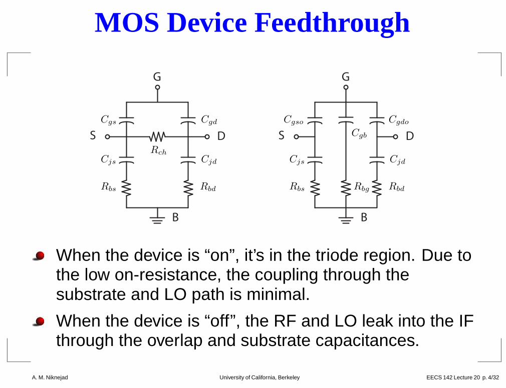
MOS Device Feedthrough
Cgs Cgd
CjdCjs
Rbs Rbd
RchCjdCjs
Rbs Rbd
Cgso Cgdo
Cgb
Rbg
G
S D
B
G
S D
B
When the device is “on”, it’s in the triode region. Due tothe low on-resistance, the coupling through thesubstrate and LO path is minimal.
When the device is “off”, the RF and LO leak into the IFthrough the overlap and substrate capacitances.
A. M. Niknejad University of California, Berkeley EECS 142 Lecture 20 p. 4/32 – p. 4/32

Summary of MOS Switching Mixer
MOS passive mixer is very linear. The device is either“on” or “off” and does not impact the linearity too much.Since there is no transconductance stage, the linearityis very good.
The downside is that the MOS mixer is passive, orlossy. There is no power gain in the device.
Need large LO drive to turn devices on/off
Need to create a differential RF and LO signal. This canbe done using baluns or by using a differential LNA andLO buffer.
A. M. Niknejad University of California, Berkeley EECS 142 Lecture 20 p. 5/32 – p. 5/32
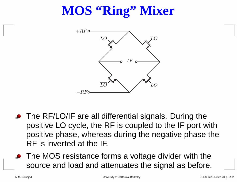
MOS “Ring” Mixer+RF
−RF
LO
LO
LO
LO
IF
The RF/LO/IF are all differential signals. During thepositive LO cycle, the RF is coupled to the IF port withpositive phase, whereas during the negative phase theRF is inverted at the IF.
The MOS resistance forms a voltage divider with thesource and load and attenuates the signal as before.
A. M. Niknejad University of California, Berkeley EECS 142 Lecture 20 p. 6/32 – p. 6/32

Passive Mixer LO Power
LO
RF IF
LO
RF IF
Since gates of the MOS switches present a largecapacitive load, a buffer is needed to drive them.
The LO buffer can be realized using larger inverters(approach “square wave”) or as a tuned buffer. A tunedlowers the power by roughly Q but has a sinusoidalwaveform .
A. M. Niknejad University of California, Berkeley EECS 142 Lecture 20 p. 7/32 – p. 7/32

LO Power (cont)
For an inverter chain driving the LO port, the powerdissipation of the last stage is given by
Pinv = CV 2
LOfLO
C is the total load presented to the LO (two MOSdevices for the double balanced mixer, one MOS devicefor single balanced).
VLO is the LO amplitude to fully turn the devices on andoff. The devices should be biased near threshold. fLO
is the LO frequency.
A. M. Niknejad University of California, Berkeley EECS 142 Lecture 20 p. 8/32 – p. 8/32

Tuned LO Power
For the tuned load case, the power is given by
Ptuned =V 2
LO
2Rt
Rt is the effective shunt resistance of the tank. Sincethe tank Q = ωLORtC, we have
Ptuned =V 2
LO
2QωLOC =
πCV 2
LOfLO
Q
A high Q tank helps to reduce the power consumptionof the LO buffer.
A. M. Niknejad University of California, Berkeley EECS 142 Lecture 20 p. 9/32 – p. 9/32

H-Bridge Ring Mixer+RF
−RF
IF LOLO
If PMOS devices are available, two CMOS invertersform an H-Bridge, applying the RF input signal to the IFdirectly during the LO cycle and inverting the RF inputat the IF output in the LO cycle.
PMOS and NMOS devices are sized appropriately tomaximize on-conductance and to minimize offcapacitance.
A. M. Niknejad University of California, Berkeley EECS 142 Lecture 20 p. 10/32 – p

RF Driver Stage
+RF
− RF
LO
LO
LO
LO
IF
L1
L2
C3 L3
Rs/2
Rs/2
If the LNA is differential, then the RF port can be driventhrough a LC matching network to maximize the RFvoltage amplitude presented to the mixer.
Note that C3 = C ′
3+ C ′′
3. The capacitance C ′
3and L3 are
used to form a resonant circuit at the RF port. Theinductor L1 and C ′′
3form an L-matching network to
boost the source RF voltage.A. M. Niknejad University of California, Berkeley EECS 142 Lecture 20 p. 11/32 – p

RF Driver Stage (cont)
+RF
L1
L3
Rs/2
C ′
3
C ′′
3
The above figure is the single-ended half circuit. Therole of the tank and L-match are now clearly dilineated.
The voltage gain of the L-match is given by
vRF = vinRt
Rt + (1 + Q2)Rs
√
Q2 + 1
where
Q =ωRF (L1 + L2)
Rs
A. M. Niknejad University of California, Berkeley EECS 142 Lecture 20 p. 12/32 – p

Time-Varying Conductance
+ IF −
+RF
−RF
g(t)
g(t− TLO/2)g(t)
g(t− TLO/2)
The RF voltage is appliedto a time varying conduc-tance. Note that if theconductance of a the LOswitches is given by g(t),then the conductance ofthe LO switches is given byg(t TLO/2).
The Thevinin equivalent source voltage is given by theopen circuit voltage
vT = vRF
(
g(t)
g(t) + g(t TLO/2)
g(t TLO/2)
g(t) + g(t TLO/2)
)
vT = vRF
(
g(t) g(t TLO/2)
g(t) + g(t TLO/2)
)
= m(t)vRF
A. M. Niknejad University of California, Berkeley EECS 142 Lecture 20 p. 13/32 – p

Time-Varying Gain m(t)
For the MOS device and a given LO waveform, thefunction m(t) can be calculated and the Fourierexpansion can be used to derive the gain.
In parctice there is a load capacitance CIF at the IF portto filter the downconverted signal. This CL complicatesthe analysis but interested students are encouraged toread the paper by Shahani, Shaeffer and Lee (JSSCvol. 32, Dec 1997, p. 2061-1071)
A. M. Niknejad University of California, Berkeley EECS 142 Lecture 20 p. 14/32 – p

“Passive” Current Mixer+LO
−LO
+IF
−IF+RF −RF
+LO
The input stage is a Gm stage similar to a Gilbert cellmixer. The Gilbert Quad, though, has no DC currentand switches on/off similar to a passive mixer.
The output signal drives the virtual ground of adifferential op-amp. The current signal is converted intoa voltage output by gthe op-amp.
A. M. Niknejad University of California, Berkeley EECS 142 Lecture 20 p. 15/32 – p
Advantages of “Passive” Current Mixer
No DC current in quad implies that there is no flickernoise generated by the switching quad. This is the keyadvantage.
The linearity is very good since the output signal is acurrent. The voltage swing does not limit the linearity ofthe mixer. This is to be contrasted to a Gilbert cell mixerwhere the voltage swing is limited due to the headroomof the switching mixer and the transconductance stage.
The op-amp output stage can be converted into an IFfilter (discussed later)
A. M. Niknejad University of California, Berkeley EECS 142 Lecture 20 p. 16/32 – p

Disadvantages of Mixer
Need large LO drive compared to the active Gilbert cellmixer.
Need an op-amp. This requires extra powerconsumption and introduces additional noise.
Need a common mode feedback circuit at the input ofthe op-amp.
A. M. Niknejad University of California, Berkeley EECS 142 Lecture 20 p. 17/32 – p

Ring or Quad?+LO
−LO
+LO
M1
M4
M3
M2
+LO
M1
−LO
M2
+LO
M4
−LO
M3
+RF
−RF
+RF −RF+IF
−IF
+IF
−IF
Note that the Gilbert quad is really a folded ring. Thusthe passive and active mixers are very similar. Themain difference is how the quad devices are biased. Inthe Gilbert cell they are biased nominally in saturationand have DC current. In the passive mixers, they arebiased near the threshold.
A. M. Niknejad University of California, Berkeley EECS 142 Lecture 20 p. 18/32 – p

Op-Amp Noise+LO
−LO
+IF
−IF
+LO
Cp
Rp
Cp
The op-amp input referred noise is amplified to IF. Theresistance seen at the op-amp input terminals isactually a switched capacitor resistor!
The parasitic capacitance at the output of thetransconductance stage is charged and discharged atthe rate of the LO.
A. M. Niknejad University of California, Berkeley EECS 142 Lecture 20 p. 19/32 – p

Switched Capacitor Resistor+LO
−LO
Cp
Ix
+Vx
−
x
+V−
Note that the parasitic capacitances are charged at therate of the LO to the input voltage Vx, and then to the
Vx, every cycle.
The total charge transferred during a period is given by
Qtot = CpVx ( CpVx) = 2CpVx
The net current is given by Ix = Qtot
TLO= 2CpVxfLO
A. M. Niknejad University of California, Berkeley EECS 142 Lecture 20 p. 20/32 – p

Switched Capacitor Resistor (cont)
Since there are two differential pairs connected to theop-amp terminals in parallel, the total charge is twice.So the effective resistance seen at this node is given by
Rp =Vx
2Ix
The effective resistance is therefore given by
Rp =1
4fLOCp
This is a switched capacitor “resistors”.
A. M. Niknejad University of California, Berkeley EECS 142 Lecture 20 p. 21/32 – p

Op-Amp Noise Transfer
+IF
−IF
Rp
Rp
Rf
Rf
The noise is thus transferred to the output with transferfunction given by
v2o =
(
1 +2Rf
Rp
)2
v2amp
To minimize this noise, we have to minimize theparasitic capacitance Cp and the op-amp noise.
A. M. Niknejad University of California, Berkeley EECS 142 Lecture 20 p. 22/32 – p

Output Filter Stage
RF
LO
IF Filter
+IF
−IF
Since a down-conversion mixer will naturally drive afilter, we see that the output current can be useddirectly to drive a current mode filter.
For instance, the op-amp can be absorbed into the firststage of a multi-stage op-amp RC IF filter. Thefeedback resistor Rf is shunted with a capacitor Cf toproduce a pole.
A. M. Niknejad University of California, Berkeley EECS 142 Lecture 20 p. 23/32 – p
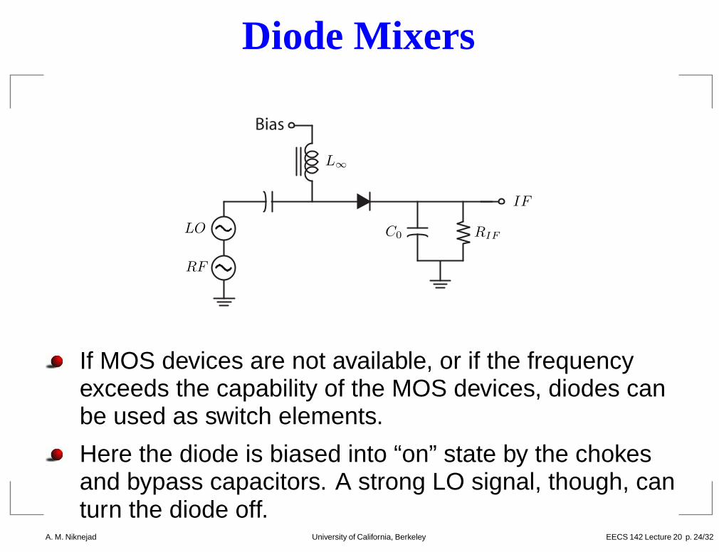
Diode Mixers
Bias
RF
IF
LO RIFC0
L∞
If MOS devices are not available, or if the frequencyexceeds the capability of the MOS devices, diodes canbe used as switch elements.
Here the diode is biased into “on” state by the chokesand bypass capacitors. A strong LO signal, though, canturn the diode off.
A. M. Niknejad University of California, Berkeley EECS 142 Lecture 20 p. 24/32 – p

Weak LO Diode Mixer
RF
IF
LO RF IF
RFLO +
The RF signal “riding” on top of the LO signal is thusmixed by the switching action.
Note that if the LO signal is weak, then mixing actionoccurs by the non-linearity of the diode. But this modehas a smaller conversion gain and produces moredistortion.
A. M. Niknejad University of California, Berkeley EECS 142 Lecture 20 p. 25/32 – p

Diode Ring Mixer
RF
IF
LO
RIF
D1
D4
D3
D2
The ring mixer is a passive mixer. Typical loss numbersare about 6 dB. The mixer has good isolation. TheLO ←→ RF isolation comes from the transformers. Thebalanced operation results in RF and LO rejection.
The LO signal drive is large since it must turn on/offdiodes.
A. M. Niknejad University of California, Berkeley EECS 142 Lecture 20 p. 26/32 – p

Mixer Description
The ring mixer is a fully balanced mixer but we have theoption of driving the LO and RF single ended. As weshall see, the LO signal alternatively turns on diodesD1/D2 or D3/D4 thereby connecting the RF voltage tothe IF with alternatively polarity.
During a positive LO voltage, the secondary of the LOtransformer applies a positive voltage across D1 inseries with the load R thereby forward biasing the diode.
Likewise, the secondary terminal of the LO transformerapplies a negative voltage to the cathode of D2, therebyforward biasing it in series with the load.
Diodes D3/D4 are reverse biased and therefore opencircuits (ideally).
A. M. Niknejad University of California, Berkeley EECS 142 Lecture 20 p. 27/32 – p

Positive LO Cycle
RF
IF
LO
RIF
Zi = 0
+
vs
−
+vs
N
−
The equivalent circuit above shows small resistorrepresenting the diode on resistance.
The RF signal is applied to the load through the centertap of the transformer. We shall show that theimpedance looking into the transformer is low (ideallyzero), and thus the entire RF signal at the secondaryterminal is applied to the load vo = vs/N
A. M. Niknejad University of California, Berkeley EECS 142 Lecture 20 p. 28/32 – p

LO Transformer
+vx
−
Zi =vx
ix
i1
i2
ZLO
Note the input impedance looking into the LOtransformer is ideally short circuit. To see this, apply atest voltage vx to this node.
If we ignore the effect of the LO signal for now, we seethat two equal currents i1 = i2 = ix/2 flow into thesecondary of the LO transformer. The return currentcomes from the center tap ground.
A. M. Niknejad University of California, Berkeley EECS 142 Lecture 20 p. 29/32 – p

LO Transformer (cont)
The induced voltage at the primary is given by
v1 = jω(M12 M13)ix/2 ≡ 0
This is because M13 = M12 and the currents on thesecondary are out of phase.
The voltages induced on the secondary side arelikewise zero (assuming perfect coupling)
v2 = jωL2ix/2 + jωM23( ix/2) ≡ 0
v3 = jωL3( ix/2) + jωM32ix/2 ≡ 0
A. M. Niknejad University of California, Berkeley EECS 142 Lecture 20 p. 30/32 – p

Negative LO CycleRF
IFRIF
Zi = 0
+
vs
−
+vs
N
−
LO
By symmetry, during the negative LO cycle, the mixersimplifies to the above equivalent circuit.
During this cycle, the RF signal is applied to the loadthrough the center tap and the bottom of thetransformer, thus producing an output signal in phasewith the RF
vo = +vs/N
A. M. Niknejad University of California, Berkeley EECS 142 Lecture 20 p. 31/32 – p
Diode Ring Mixer OperationThe operation is thus similar to the double balancedGilbert cell mixer in voltage mode. The RF voltage ismultiplied by ±1 with a rate of the LO signal.
The lack of DC means that the RF is rejected at the IFport. Likewise, the LO/RF signals are isolated by theswitches. The only feed-through occurs due to reverseisolation of the diodes.
The biggest drawback, though, is the bulkytransformers and the large LO drive. The mixer is verylinear and quite attractive in applications where linearityreigns supreme over power consumption.
At microwave frequencies, the transformers can bereplaced by couplers. Since diodes can operate up toextremely high frequencies (THz), the entire circuit canwork up to THz region.
A. M. Niknejad University of California, Berkeley EECS 142 Lecture 20 p. 32/32 – p