Embed Size (px)
Citation preview

Lecture 130 – VCOs (6/10/03) Page 130-1
ECE 6440 - Frequency Synthesizers © P.E. Allen - 2003
LECTURE 130 – VOLTAGE-CONTROLLED OSCILLATORS(READING: [4,6,9])
ObjectiveThe objective of this presentation is examine and characterize the types of voltage-controlled oscillators compatible with both discrete and integrated technologies.Outline
• Characterization of VCO’s• Oscillators
- RC- LC- Relaxation oscillators- Ring oscillators- Direct digital synthesis (DDS)
• Varactors• Summary
Lecture 130 – VCOs (6/10/03) Page 130-2
ECE 6440 - Frequency Synthesizers © P.E. Allen - 2003
CHARACTERIZATION OF VOLTAGE-CONTROLLED OSCILLATORSIntroduction to Voltage-Controlled OscillatorsWhat is an oscillator?
An oscillator is a circuit capable of maintaining electric oscillations.An oscillator is a periodic function, i.e. f(x) = f(x+nk) for all x and for all integers, n,and k is a constant.All oscillators use positive feedback of one form or another.Classification of oscillators:
Oscillators
Tuned Oscillators Untuned Oscillators
RCOscillators
SCOscillators
LCOscillators
CrystalOscillators
RelaxationOscillators
RingOscillators
Fig. Osc-01
What are tuned oscillators?A tuned oscillator uses a frequency-selective or tuned-circuit in the feedback
path and is generally sinusoidal.An untuned or oscillator uses nonlinear feedback and is generally non-sinusoidal

Lecture 130 – VCOs (6/10/03) Page 130-3
ECE 6440 - Frequency Synthesizers © P.E. Allen - 2003
Types of OscillatorsRing Oscillator:
Cascade of inverters
Frequency of oscillation = 1
Σ of stage delays
Controlled by current or power supplyHigher power
LC Oscillator:
Frequency of oscillation = 1LC
Controlled by voltage dependent capacitance (varactor)Medium power
Relaxation Oscillator:Frequency determined by circuit time constantsControlled by currentMedium power
RC Oscillators:Don’t require inductorsOperate at lower frequencies (1-100MHz)
Lecture 130 – VCOs (6/10/03) Page 130-4
ECE 6440 - Frequency Synthesizers © P.E. Allen - 2003
Characteristics of Oscillators• Frequency of oscillation• Frequency tuning range as a function of the controlling variable (either voltage or
current)• Frequency stability – phase noise and jitter• Amplitude stability (adjustable?)• Purity (harmonics)

Lecture 130 – VCOs (6/10/03) Page 130-5
ECE 6440 - Frequency Synthesizers © P.E. Allen - 2003
Linear Feedback Oscillator SystemSimplified block diagram:
-
Vin VoutA(jw)
F(jw)Vf
Fig. Osc-02
The loop gain of this diagram is,LG(jω) = A(jω)F(jω)
When the loop gain is equal to 1, oscillation occurs.Re[LG(jω)] + Im[LG(jω)] = 1 + j0
The frequency of oscillation is found from,Im[LG(jω)] = 0
and the gain necessary for oscillation is found from,Re[LG(jω)] = 1
Lecture 130 – VCOs (6/10/03) Page 130-6
ECE 6440 - Frequency Synthesizers © P.E. Allen - 2003
Linear Oscillator Amplitude StabilizationWhat determines the amplitude of the oscillator? Good question.
A(jω) and/or F(jω) must have an output-input characteristic that looks like an sshape.
For small amplitudes, the magnitude of the loop gain is greater than one and theoscillation grows.
As the amplitude grows, the effective gain decreases and stabilizes at just theright amplitude to give an effective loop gain of unity.Illustration:
vin
vout
Effective LoopGain = 1
Peak-to-peakamplitude
jω
σ
Pole Locations as a function of amplitudeFig. Osc-03

Lecture 130 – VCOs (6/10/03) Page 130-7
ECE 6440 - Frequency Synthesizers © P.E. Allen - 2003
Van der Pol Equations for OscillatorsBasic RLC oscillator and negative resistance circuit:
-RiL iC iR
i
+
-
v v
i
VanderPol
L C Rp
iL + iC + iR + i = 0 and i = f(v) = -a1v + a3v3
vL = LdiLdt →
diLdt =
vL
didv = -a1 + 3a3v2
iC = Cdvdt →
diCdt = C
d2vdt2
didv |
v=0 = -a1 = - 1
Rn
iR = v
Rp →
diRpdt =
1Rp
dvdt
didt = -a1
dvdt + 3a3v2
dvdt
diLdt +
diCdt +
diRpdt +
didt = 0 →
vLL + C
d2vdt2 +
1Rp
dvdt +
-a1dvdt + 3a3v2
dvdt = 0
C d2vdt2 +
1
Rp - a1 + 3a3v2
dvdt +
vL = 0
d2vdt2 +
1
CRp -
a1C +
3a3v2
C dvdt +
vLC = 0
Lecture 130 – VCOs (6/10/03) Page 130-8
ECE 6440 - Frequency Synthesizers © P.E. Allen - 2003
Van der Pol EquationsAt start up, v is very small so that 3a3v2 ≈ 0
∴ s2V(s) +
1
Rp - a1
C sV(s) + V(s)LC = 0 → s2 + ms +
1LC = 0
Poles = - 0.5m ±0.5 m2 - 4
LC = -0.5m ± j0.54
LC - m2
For jω axis poles, m = 0.In steady-state, the following relationship must hold.
m =
1
CRp -
a1C +
3a3v2
C = 0
We see that the amplitude of oscillation (ωosc = 1LC ) will be,
V = a1 -
1Rp
3a3 =
1Rn
- 1
Rp3a3
For V = 1V, 1
Rn =
1Rp
- 3a3

Lecture 130 – VCOs (6/10/03) Page 130-9
ECE 6440 - Frequency Synthesizers © P.E. Allen - 2003
Open-Loop Concept of an OscillatorBasic closed-loop oscillator:
H(jω)X(jω) Y(jω)
Frequency shaping network & amplifier
Fig. 12.4-5
+
+
Oscillator oscillates when H(jω) = 1+j0Open-loop Q:
The open-loop Q is a measure of how much the closed loop system opposesvariations in the oscillation frequency. The higher the Q, the lower the phase noise.Definitions of Q:
1.) Q = ωo∆ω where ωo is the frequency of oscillation.
2.) Q = 2π·Energy Stored
Energy Dissipated per Cycle
3.) Q = ωo2
ddω
Arg[H(jω)]
1.00.707
∆ω
ωoω
Fig. 12.4-6
Lecture 130 – VCOs (6/10/03) Page 130-10
ECE 6440 - Frequency Synthesizers © P.E. Allen - 2003
Voltage Controlled Oscillators - TuningA voltage controlled oscillator (VCO) is an oscillator whose frequency can be varied by avoltage (or current).In local oscillator applications, the VCO frequency must be able to be varied over the Rxor Tx range (quickly).
Freq
uenc
y
Tx or RxRange
Voltage tuning range
Linear tuning
Nonlineartuning
Fig. 12.3-4
Tuning variables:• Capacitance (varactor)• Current• Power supply
Speed of tuning will be determined by the bandwidth of the phase lock loop.

Lecture 130 – VCOs (6/10/03) Page 130-11
ECE 6440 - Frequency Synthesizers © P.E. Allen - 2003
OSCILLATORSRC Oscillators - Wien-Bridge OscillatorCircuit:
Open-Loop Gain: For simplicity, let R1 = R2 = R and C1 = C2 = C.
∴ LG(s) = K
sRC
s2 + 3
RC s + 1
(RC)2
→ LG(jω) = K
jωRC
1
(RC)2 - ω2 + 3
RC jω
Equating the loop gain to 1+j0 gives
K jωοRC
1
(RC)2 - ωο2 + 3
RC jωο
= 1 + j0
The only way this equation can be satisfied is if ωo2 =
1RC and K =3.
Vout
R1
K
R2
C1
C2
A B
Fig. Osc-04
Lecture 130 – VCOs (6/10/03) Page 130-12
ECE 6440 - Frequency Synthesizers © P.E. Allen - 2003
Wien-Bridge Oscillator – ContinuedHow do you realize the amplifier of K = 3?
VoutVin
= 1+ R2R1
How does the amplitude stabilize?• Thermistor (a resistor whose resistance decreases with increasing temperature)• Nonlinear transfer functionExample:
vin vout
+-
V1D1
V2
D2
R1 R1
R2 R2
R3
R4
+-
R KR
vout
vin
Slope = R4R3
R42R2
+
Slope = R4R3
R42R1
+
Slope = R42R1
R42R1
+ R4R3
+
2V12V2
Fig. Osc-06
VinVout
+-
R1R2
Fig. Osc-05

Lecture 130 – VCOs (6/10/03) Page 130-13
ECE 6440 - Frequency Synthesizers © P.E. Allen - 2003
Other RC OscillatorsRC Phase-Shift Oscillator:
If R1 = R2 = R3 = R and C1 = C2 = C3 = C, then
LG(jω) = (R4R3)(jωRC)(ωRC)2
[1-6(ωRC)2] + jωRC [5 -(ωRC)2]
∴ ωosc = 1
6 RC and K = R4R3
= 29
Quadrature Oscillator:
LG(jω) = -1
(jω)2R1C2R3C4
∴ ωosc = 1
R1C2R3C4
Other RC oscillators: Twin-tee RC oscillator, Sallen-Key bandpass filter with Q = ∞,Infinite gain, bandpass filter with Q = ∞How do you tune the RC oscillator?
Must vary either R or C or both.
vout
+-
R1 R2
R3 R4
C1
C2 C3
Fig. Osc-07
Vout
+-R3 C4
+-R R
+-
R1
C2
Fig. Osc-08
Lecture 130 – VCOs (6/10/03) Page 130-14
ECE 6440 - Frequency Synthesizers © P.E. Allen - 2003
ExampleThe circuit shown is a RC oscillator. Find thefrequency of oscillation in Hertz and the voltagegain, K, of the voltage amplifiers necessary foroscillation. The voltage amplifiers have infiniteinput resistance and zero output resistance.
SolutionThe loop gain can be found from the schematicshown:
T(s) = VrVx
= K2
1
sRC+1
sRC
sRC+1
= K2sRC
s2R2C2 + 2sRC + 1 → T(jω) = K2jωRC
1-ω2R2C2 + jω 2RC = 1 + j0
We see from this equation that for oscillation to occur, the following conditions must besatisfied:
1-ω2R2C2 = 0 and K2 = 2or
ωosc = 1
RC = 1
104·10−9 = 105 radians/sec. → fosc = 15.9kHz and K = 2 = 1.414
K KVout
C = 1nF
C =1nF
R = 10kΩ
R =10kΩ
S03FEP1
K KVr
C = 1nF
C =1nF
R = 10kΩ
R =10kΩ
S03FES1
Vx

Lecture 130 – VCOs (6/10/03) Page 130-15
ECE 6440 - Frequency Synthesizers © P.E. Allen - 2003
Gm-C OscillatorsSame the quadrature oscillator only implemented in a more IC friendly manner.
gm1+
-gm2
+
-
C2C1
Vo1Vo2
Fig. 130-02
Vo1
t
Vo2
t
Open Loop Gain = L(s) =
gm1
sC1
-gm2
sC2 =
-gm1gm2s2C1C2
Letting s = jω and setting L(jω) = 1 gives,
ωosc = gm1gm2C1C2
= gm1 C1
= gm2C2
if gm1 = gm2 and C1 = C2
This circuit is much easier to tune. If the transconductors are MOS transistors, then
gm = 2K'IDW
L
Varying the bias current will vary gm and tune the frequency.
Lecture 130 – VCOs (6/10/03) Page 130-16
ECE 6440 - Frequency Synthesizers © P.E. Allen - 2003
Switched Capacitor OscillatorsConcept
Theoretically, the R’s of any RC oscillator can be replaced by switches andcapacitors to create an SC oscillator.Quadrature SC Oscillator
+-
V1(z)C1
φ1φ2
α1C1
+-
C2
φ1
φ2
α2C2
φ2
φ1
Vout(z)ee
Fig. Osc-09
φ1φ2
ωosc = α1α2
T2 = α1α2 fclock (really a frequency translator)
The output is a sinusoid at frequency of α1α2 fclock.
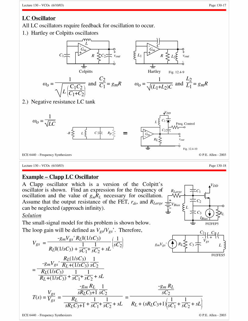
Lecture 130 – VCOs (6/10/03) Page 130-17
ECE 6440 - Frequency Synthesizers © P.E. Allen - 2003
LC OscillatorAll LC oscillators require feedback for oscillation to occur.1.) Hartley or Colpitts oscillators
+-Gm
L
C1 C2R+
-vout
Colpitts
+-Gm
C
L1 L2R+
-vout
Hartley Fig. 12.4-9
ωo = 1
L
C1C2
C1+C2
and C2C1 = gmR ωo =
1(L1+L2)C and
L2L1 = gmR
2.) Negative resistance LC tank
ωo = 1LC
L C-R Rp+-Gm
C1L
+
-vout
Fig. 12.4-10
VDD
C2
Freq. Control
RL
Lecture 130 – VCOs (6/10/03) Page 130-18
ECE 6440 - Frequency Synthesizers © P.E. Allen - 2003
Example – Clapp LC OscillatorA Clapp oscillator which is a version of the Colpitt’soscillator is shown. Find an expression for the frequency ofoscillation and the value of gmRL necessary for oscillation.Assume that the output resistance of the FET, rds, and RLargecan be neglected (approach infinity).SolutionThe small-signal model for this problem is shown below.The loop gain will be defined as Vgs/Vgs’. Therefore,
Vgs = -gmVgs' RL||(1/sC3)
RL||(1/sC3) + 1
sC1+
1sC2
+ sL
1
sC2
= -gmVgs'
RL(1/sC3) RL +(1/sC3)
1sC2
RL(1/sC3)
RL +(1/sC3) + 1
sC1+
1sC2
+ sL
T(s) = VgsVgs
=
-gm RLsRLC3+1
1sC2
RL
sRLC3+1 + 1
sC1+
1sC2
+ sL =
-gm RLsC2
RL + (sRLC3+1)
1
sC1 +
1sC2
+ sL
VDD
RLarge
VBiasL
C1
C2
C3IBias
F02FEP5
RL
gmVgs'Vgs
RL C3
C2 C1
L
+-
F02FES5

Lecture 130 – VCOs (6/10/03) Page 130-19
ECE 6440 - Frequency Synthesizers © P.E. Allen - 2003
Example – Continued
T(s) = -gm RL
sC2RL + (sRLC3+1)(s2LC2+ C2C1
+ 1)
T(s) = -gm RL
sC2RL +s3RLC3LC2+ sRLC2C3
C1 + sC3RL + s2LC2 +
C2C1
+1
T(jω) = -gm RL
[1+ C2C1
- ω2LC2] + jω[RL (C2+C3) + RLC2C3
C1 -ω2RLC3LC2] = 1 + j0
∴ C2+C3 + C2C3C1 = ωosc2C3LC2 → ωosc =
1L
1
C1 +
1C2
+ 1
C3
Also, gm RL = ωosc2LC2 –1 - C2C1
= C2
1
C1 +
1C2
+ 1
C3 -
C2C1
-1 = C2C3
→ gm RL = C2C3
Lecture 130 – VCOs (6/10/03) Page 130-20
ECE 6440 - Frequency Synthesizers © P.E. Allen - 2003
LC OscillatorsCircuits:
VDD
L LC
M1 M2
vo2vo1
VDD
L L
C
M1 M2
vo2vo1
PMOS LC Oscillator NMOS LC Oscillator
VDD
L LC
M1 M2
vo2vo1
L2nd Harmonictrap
Improved NMOS LC OscillatorFig. 12.4-10A
C2
Conditions for oscillation:
H(s) =
gm
C s
s2 + s
RC + 1
LC 2
⇒ H(jω) =
gm
C jω
-ω2 + jωRC +
1LC
2
= 1+j0 ⇒ ωosc2 = 1
LC & gmC = 1
Output swing of the improved circuit is twice that of the other circuits plus the secondharmonic is removed.

Lecture 130 – VCOs (6/10/03) Page 130-21
ECE 6440 - Frequency Synthesizers © P.E. Allen - 2003
Example – LC OscillatorAn LC oscillator is shown. The value of the inductors, L, are 5nHand the capacitor, C, is 2.5pF. If the Q of each inductor is 5, find (a.)the value of negative resistance that should be available from thecross-coupled, source-coupled pair (M1 and M2) for oscillation and(b.) design the W/L ratios of M1 and M2 to realize this negativeresistance (if you can’t find the negative resistance of part (a.)assume that the desired negative resistance is -100Ω).
Solution
(a.) The equivalent circuit seen by the negative resistance circuit is:
The frequency of oscillation is given as 1/ 2LC or ωo = 2πx109
radians/sec.Therefore the series resistance, Rs, is found as
Rs = ωLQ =
2πx109·5x10-9
5 = 2π Ω
Converting the series impedance of 2L and 2Rs into a parallelimpedance gives,
Y = 1
2Rs+jω2L = 0.5
Rs+jωL · Rs-jωL Rs-jωL =
0.5RsRs2+ω2L2 - j
0.5ωLsRs2-ω2L2
L LC
VDD
M1 M2
2mA
F00E2P2
2L 2Rs
C
F00E2S2A
Lecture 130 – VCOs (6/10/03) Page 130-22
ECE 6440 - Frequency Synthesizers © P.E. Allen - 2003
LC Oscillator Example - ContinuedThe reciprocal of the conductance is the parallel resistance, Rp, given as
Rp = Rs2+ω2L2
0.5Rs =
4π2 + 4π2·25π = 4π(26) = 326.7Ω
∴ Rneg = -104π Ω = -326.7Ω
(b.) The negative resistance seen by the RLC circuit is found asfollows.
iin = gm1vgs1 = - gm2vgs2
∴ Rin = viniin =
vgs2-vgs1iin =
-1gm2
- 1
gm1 =
-2gm
Assuming the 2mA splits evenly between M1 and M2 for thenegative resistance calculation gives,
Thus, gm = gm1 = gm2 = 2·2mA·110x10-6 (W/L) = W/L
1508 = 2
104π
∴ W/L =
1508
52π2 = 841 ⇒ W/L = 841
M1 M2
2mA
F00E2S2B
vin
iin
+-
vgs1+-
vgs2

Lecture 130 – VCOs (6/10/03) Page 130-23
ECE 6440 - Frequency Synthesizers © P.E. Allen - 2003
LC OscillatorVCO with PMOS pair:
Design:• Inductors - L1 = L2 = 7.1nH, Q = 8.5 at
910MHz (Metal 3 with spacing of 2.1µm and width of16.1µm and 5 turns)
• R1, C1 and R2, C2 form ac coupling filters• Buffers A and B isolate the VCO from the next stages to
avoid the pulling effect of the center frequency due toinjection from the external load or the prescaler fed bythe VCO. Buffer A provides a matched 50Ω outputimpedance and buffer B drives the large capacitance ofthe prescaler.
• ISS = 1.5mA0 1 2 3
850
900
950
1000
Control Voltage (V)
VC
O F
requ
ency
(M
Hz)
Fig. 12.4-12
ISS
VDD
M1 M2
Cv2 Cv2VControl
L1 L1
C1
C2
R1 R2
BufferA
BufferB
Output
Prescaler
Fig. 12.4-11
Lecture 130 – VCOs (6/10/03) Page 130-24
ECE 6440 - Frequency Synthesizers © P.E. Allen - 2003
Relaxation OscillatorsCircuit:
Open Loop:Assume that C in the closed loop circuit is really two 2C capacitors in series
and ground the midpoint to obtain the open-loop circuit. C1 and C2 are capacitancesto ground from the drains of M1 and M2.
H(s) =
-gmRCAs
(gm + CAs)(RCDs + 1)2
where gm = transconductance of each transistor and CD = C1 = C2.It can be shown that,
ωo = gm
RCACD and Q = 4
1 - CDCA
CDCA ⇒ Qmax =1 ⇒ Soθ(fm) =
14
fo
fm
2 Sθ (fm)
ISS ISSC
M1 M2
R R
VDD
Closed-Loop
ISS
M1
R
VDD
Open-Loop
CA
C1
M2
R
CA
C2
ISS
Fig. 12.4-13

Lecture 130 – VCOs (6/10/03) Page 130-25
ECE 6440 - Frequency Synthesizers © P.E. Allen - 2003
Relaxation Oscillator - Experimental Results
ISS ISSC
M1 M2
R R
VDD
W/L = 100µm/0.5µmgm = 1/84µS
R = 275Ω
C = 0.6pF
ISS = 3mA
Fig. 12.4-14
fo = 920 MHzPhase noise = -105 dBc/Hz for fm = 1MHz and -115dBc/Hz for fm = 5MHz
Lecture 130 – VCOs (6/10/03) Page 130-26
ECE 6440 - Frequency Synthesizers © P.E. Allen - 2003
Ring Oscillator VCOThree-stagering oscillator:
Comparison ofa Three-Stageand Four-StageRing Oscillator:
Characteristic 3-Stage Ring Oscillator 4-Stage Ring OscillatorMin. Required Gain 2 2 Noise ShapingFunction
127
fo
fm2
116
fo
fm2
Open-Loop Q 0.75 2 2Power Dissipation 1.8mW 3.6mW
+
-
-
+
+
-
-
+
+
-
-
+
-
+Output
FrequencyControl
+
-
-
+-
+
-
+
-
+
M1 M2
M3 M4
M5 M6
VDD
Input
Output
Frequency Control
Fig. 12.4-4

Lecture 130 – VCOs (6/10/03) Page 130-27
ECE 6440 - Frequency Synthesizers © P.E. Allen - 2003
Ring Oscillator - Experimental Results
-
+
-
+ M1 M2
M3 M4
M5
VDD
Input
Output
Frequency ControlFig. 12.4-8
M1 and M2: W/L = 97µm/0.5µmgm = 1/214µS
M3 and M4: W/L = 13.4µm/0.5µmgm = 1/630µS
M5: W/L = 13.4µm/0.5µmID = 790µAgm = 1/530µS
fo = 2.2GHz
Phase noise at 1MHz = -99.2 dBc/HzGeneral Comments:
Phase noise is proportional to power dissipationWide tuning range (2 to 1)Poor phase noise performance
Lecture 130 – VCOs (6/10/03) Page 130-28
ECE 6440 - Frequency Synthesizers © P.E. Allen - 2003
Direct Digital Frequency Synthesizer - DDFSA sinusoid is digitized and stored in a ROM. These stored values are applied to
a DAC at regular time intervals by a reference clock. The frequency is increased bytaking fewer , but further separated samples from the ROM look-up table.Block Diagram:
Operation:1.) Phase accumulator adds the frequency setting data to the previous contents onceevery clock cycle. The most significant bits of the results are used to address theROM look-up table.2.) The address decoding circuitry of the ROM selects the corresponding N bitsample and feeds it to the DAC.3.) The DAC converts this digital data to an analog signal.4.) The analog signal is passed through the low-pass filter to smooth the waveformand remove out-of-band high frequency noise from the signal.Advantages: Disadvantages:
• Very high frequency resolution (fclock/2N)• Fast switching time
• High power consumption• Restricted to low frequencies
FrequencySetting Data
L bits M bits N bits
PhaseAccumulator
Sine look-uptable in ROM DAC LPF Output
ReferenceClock
Fig. 12.4-15

Lecture 130 – VCOs (6/10/03) Page 130-29
ECE 6440 - Frequency Synthesizers © P.E. Allen - 2003
Quadrature VCO’sPolyphase Oscillator:
Oscillator B
180° 270°0° 90°
Oscillator A
Fig. 12.5-14
• Two cross-coupled oscillators synchronize in exact quadrature• Phase inaccuracy insensitive to mismatch in resonators• Large amplitudes available, balanced oscillation available to drive mixer FETsPerformance:
830 MHzUnwanted sideband -46 dB below wanted sidebandLeakage 49 dB below wanted sideband
Lecture 130 – VCOs (6/10/03) Page 130-30
ECE 6440 - Frequency Synthesizers © P.E. Allen - 2003
Quadrature OscillatorsFrequency Division Approach:
+-
÷2FrequencyDoubler
BPF
K1sin(ßt)
K1cos(ßt)
LO∠90°I
Q
Fig. 12.5-13
LO
Comments:• Start with a single phase local oscillator at twice the desired frequency• Divide by 2 is done by positive and negative edge triggered flip-flops• Phase accuracy depends on timing skews between the flip-flop channels (typically 1-2°)

Lecture 130 – VCOs (6/10/03) Page 130-31
ECE 6440 - Frequency Synthesizers © P.E. Allen - 2003
VARACTORS – VARIABLE CAPACITORSOne of the components that can be used to vary the frequency is the capacitor.Types of Capacitors Considered• pn junction capacitors• Standard MOS capacitors• Accumulation mode MOS capacitors• Poly-poly capacitors• Metal-metal capacitorsCharacterization of CapacitorsAssume C is the desired capacitance:1.) Dissipation (quality factor) of a capacitor is
Q = ωCRp
where Rp is the equivalent resistance in parallel with the capacitor, C.
2.) Cmax/Cmin ratio is the ratio of the largest value of capacitance to the smallest whenthe capacitor is used as a variable capacitor.
3.) Variation of capacitance with the control voltage.4.) Parasitic capacitors from both terminal of the desired capacitor to ac ground.
Lecture 130 – VCOs (6/10/03) Page 130-32
ECE 6440 - Frequency Synthesizers © P.E. Allen - 2003
Desirable Characteristics of Varactors1.) A high quality factor2.) A control voltage range compatible with supply voltage3.) Good tunability over the available control voltage range4.) Small silicon area (reduces cost)5.) Reasonably uniform capacitance variation over the available control voltage range6.) A high Cmax/Cmin ratio
Some References for Further Information1.) P. Andreani and S. Mattisson, “On the Use of MOS Varactors in RF VCO’s,” IEEEJ. of Solid-State Circuits, vol. 35, no. 6, June 2000, pp. 905-910.2.) A-S Porret, T. Melly, C. Enz, and E. Vittoz, “Design of High-Q Varactors for Low-Power Wireless Applications Using a Standard CMOS Process,” IEEE J. of Solid-StateCircuits, vol. 35, no. 3, March 2000, pp. 337-345.3.) E. Pedersen, “RF CMOS Varactors for 2GHz Applications,” Analog IntegratedCircuits and Signal Processing, vol. 26, pp. 27-36, Jan. 2001

Lecture 130 – VCOs (6/10/03) Page 130-33
ECE 6440 - Frequency Synthesizers © P.E. Allen - 2003
Digitally Varied CapacitancesIn a digital process, high-quality capacitors are very difficult to achieve. A high-qualityvariable capacitor is even more difficult to realize.Therefore, digitally controlled capacitances are becoming more popular.
S1 S2 S3 S4
C C2
C4
C8
2C 2C
4C 4C
8C 8C
16C 16C
S1
S2
S3
S4Single-Ended
DifferentialFig. 3.1-44
VFine Tune
VFine Tune
Concerns:• Switch parasitics• Switch ON resistance (will lower Q)
Lecture 130 – VCOs (6/10/03) Page 130-34
ECE 6440 - Frequency Synthesizers © P.E. Allen - 2003
Kvo of Digitally Tuned VCOs
The value of the VCO gain constant can be made smaller which is desirable in manyapplications of the VCO.
VC
O F
requ
ency
Contolling Voltage(Fine tune)
DigitallyAdjustableCapacitors
Fig. 3.1-45
VmaxVmin

Lecture 130 – VCOs (6/10/03) Page 130-35
ECE 6440 - Frequency Synthesizers © P.E. Allen - 2003
Capacitor Errors1.) Oxide gradients2.) Edge effects3.) Parasitics4.) Voltage dependence5.) Temperature dependence
Lecture 130 – VCOs (6/10/03) Page 130-36
ECE 6440 - Frequency Synthesizers © P.E. Allen - 2003
Capacitor Errors - Oxide GradientsError due to a variation in oxide thickness across the wafer.
y
x1 x2 x1
A1 A2 B
A1 B A2
No common centroidlayout
Common centroidlayout
Only good for one-dimensional errors.An alternate approach is to layout numerous repetitions and connect them randomly toachieve a statistical error balanced over the entire area of interest.
A B C
A
A
B
B
C
C
A B C
A
A
B
B
C
C
A B C
A
A
B
B
C
C
0.2% matching of poly resistors was achieved using an array of 50 unit resistors.

Lecture 130 – VCOs (6/10/03) Page 130-37
ECE 6440 - Frequency Synthesizers © P.E. Allen - 2003
Capacitor Errors - Edge EffectsThere will always be a randomness on the definition of the edge.However, etching can be influenced by the presence of adjacent structures.For example,
AC
A BC
B
Matching of A and B are disturbed by the presence of C.
Improved matching achieve by matching the surroundings of A and B.
Lecture 130 – VCOs (6/10/03) Page 130-38
ECE 6440 - Frequency Synthesizers © P.E. Allen - 2003
Capacitor Errors - Area/Periphery RatioThe best match between two structures occurs when their area-to-periphery ratios areidentical.Let C’1 = C1 ± ∆C1 and C’2 = C2 ± ∆C2
whereC’ = the actual capacitanceC = the desired capacitance (which is proportional to area)∆C = edge uncertainty (which is proportional to the periphery)
Solve for the ratio of C’2/C’1,
C’2C’1
= C2 ± ∆C2C1 ± ∆C1
= C2C1
1 ± ∆C2C2
1 ± ∆C1C1
≈ C2C1
1 ± ∆C2C2
1 -+ ∆C1C1
≈ C2C1
1 ± ∆C2C2
-+ ∆C1C1
If ∆C2C2
= ∆C1C1
, then C’2C’1
= C2C1
Therefore, the best matching results are obtained when the area/periphery ratio of C2 isequal to the area/periphery ratio of C1.

Lecture 130 – VCOs (6/10/03) Page 130-39
ECE 6440 - Frequency Synthesizers © P.E. Allen - 2003
Capacitor Errors - Relative AccuracyCapacitor relative accuracy is proportional to the area of the capacitors and inverselyproportional to the difference in values between the two capacitors.For example,
0.04
0.03
0.02
0.01
0.001 2 4 8 16 32 64
Unit Capacitance = 0.5pF
Unit Capacitance = 1pF
Unit Capacitance = 4pF
Rel
ativ
e A
ccur
acy
Ratio of Capacitors
Lecture 130 – VCOs (6/10/03) Page 130-40
ECE 6440 - Frequency Synthesizers © P.E. Allen - 2003
Capacitor Errors - ParasiticsParasitics are normally from the top and bottom plate to ac ground which is typically thesubstrate.
Top Plate
Bottom Plate
Desired Capacitor
Topplate
parasiticBottom
plateparasitic
Top plate parasitic is 0.01 to 0.001 of Cdesired
Bottom plate parasitic is 0.05 to 0.2 Cdesired

Lecture 130 – VCOs (6/10/03) Page 130-41
ECE 6440 - Frequency Synthesizers © P.E. Allen - 2003
Other Considerations on Capacitor AccuracyDecreasing Sensitivity to Edge Variation:
A A'
B B'
A A'
B B'
Sensitive to edge variation in both upper andlower plates
Sensitive to edge varation inupper plate only. Fig. 2.6-13
A structure that minimizes the ratio of perimeter to area (circle is best).
Top Plateof Capacitor
Fig. 2.6-14
Bottom plateof capacitor
Lecture 130 – VCOs (6/10/03) Page 130-42
ECE 6440 - Frequency Synthesizers © P.E. Allen - 2003
Definition of Temperature and Voltage CoefficientsIn general a variable y which is a function of x, y = f(x), can be expressed as a Taylorseries,
y(x = x0) ≈ y(x0) + a1(x- x0) + a2(x- x0)2+ a1(x- x0)3 + ···
where the coefficients, ai, are defined as,
a1 = df(x)dx
|x=x0 , a2 =
12
d2f(x)dx2
|x=x0 , ….
The coefficients, ai, are called the first-order, second-order, …. temperature or voltagecoefficients depending on whether x is temperature or voltage.Generally, only the first-order coefficients are of interest.
In the characterization of temperature dependence, it is common practice to use a termcalled fractional temperature coefficient, TCF, which is defined as,
TCF(T=T0) = 1
f(T=T0) df(T)dT
|T=T0 parts per million/°C (ppm/°C)
or more simply,
TCF = 1
f(T) df(T)dT parts per million/°C (ppm/°C)
A similar definition holds for fractional voltage coefficient.

Lecture 130 – VCOs (6/10/03) Page 130-43
ECE 6440 - Frequency Synthesizers © P.E. Allen - 2003
Capacitor Errors - Temperature and Voltage Dependence
Polysilicon-Oxide-Semiconductor CapacitorsAbsolute accuracy ≈ ±10%Relative accuracy ≈ ±0.2%Temperature coefficient ≈ +25 ppm/C°Voltage coefficient ≈ -50ppm/V
Polysilicon-Oxide-Polysilicon CapacitorsAbsolute accuracy ≈ ±10%Relative accuracy ≈ ±0.2%Temperature coefficient ≈ +25 ppm/C°Voltage coefficient ≈ -20ppm/V
Accuracies depend upon the size of the capacitors.
Lecture 130 – VCOs (6/10/03) Page 130-44
ECE 6440 - Frequency Synthesizers © P.E. Allen - 2003
SUMMARY• Characterization of VCO’s
- Frequency,- Frequency tuning range- Frequency stability- Amplitude stability- Spectral purity
• Oscillators- RC- LC- Relaxation oscillators- Ring oscillators- Direct digital synthesis (DDS)
• VaractorsUsed to vary the frequency of RC and LC oscillators