Embed Size (px)
Citation preview

5/17/2018 Learning Material - VLSI Design - slidepdf.com
http://slidepdf.com/reader/full/learning-material-vlsi-design 1/172
Design of System Elements
Basics of VLSI

5/17/2018 Learning Material - VLSI Design - slidepdf.com
http://slidepdf.com/reader/full/learning-material-vlsi-design 2/172
Jamadagni H S 2 of 5 0 ITC/V1/2004
A Generic Digital Machine
MEMORY
DATAPATH
CONTROL
I N P U T - O U T P U T

5/17/2018 Learning Material - VLSI Design - slidepdf.com
http://slidepdf.com/reader/full/learning-material-vlsi-design 3/172
Jamadagni H S 3 of 5 0 ITC/V1/2004
Mem or y
Con t ro l
I n t e rconn ect
Building Blocks for Digital Architectures
• Arithmetic unit
– Data path (adder, multiplier, shifter, comparator):Bit slice technique
• Memory
– RAM, ROM, PROM, Flash Memory…….
• Random logic– Finite state machine, Switches, Arbiters
• Data vehicle
– Buses for data, address and control

5/17/2018 Learning Material - VLSI Design - slidepdf.com
http://slidepdf.com/reader/full/learning-material-vlsi-design 4/172
Jamadagni H S 4 of 5 0 ITC/V1/2004
Bit-Sliced Design
Bit 3
Bit 2
Bit 1
Bit 0 R e g i s t e r
A d d
e r
S h i f t e r
M
u l t i p l e x e r
Cont ro l
D a t a - I n
D a t a
- O u t
Ti le id ent ical p r ocess ing e lem ent s

5/17/2018 Learning Material - VLSI Design - slidepdf.com
http://slidepdf.com/reader/full/learning-material-vlsi-design 5/172
Jamadagni H S 5 of 5 0 ITC/V1/2004
Full-Adder
A B
Cout
Sum
Cin Fulladder

5/17/2018 Learning Material - VLSI Design - slidepdf.com
http://slidepdf.com/reader/full/learning-material-vlsi-design 6/172
Jamadagni H S 6 of 5 0 ITC/V1/2004
The Binary Adder
S A B Ci
⊕=
A= BCi ABCi ABCi ABC+ + +
Co
AB BCi
ACi
+ +=
A B
Cout
Sum
Cin Fulladder

5/17/2018 Learning Material - VLSI Design - slidepdf.com
http://slidepdf.com/reader/full/learning-material-vlsi-design 7/172
Jamadagni H S 7 of 5 0 ITC/V1/2004
Express Sum and Carry as a function of P, G, D
Define 3 new variable which ONLY depend on A, B
Generate (G) = AB
Propagate (P) = A ⊕ B
Delete = A B
Can also derive expressions for S and C o based on D and P

5/17/2018 Learning Material - VLSI Design - slidepdf.com
http://slidepdf.com/reader/full/learning-material-vlsi-design 8/172
Jamadagni H S 8 of 5 0 ITC/V1/2004
The Ripple-Carry Adder
A0 B0
S0
C o,0C i,0
A1 B1
S1
C o,1
A2 B2
S2
C o,2
A3 B3
S3
C o,3
(= C i,1)FA FA FA FA
Worst case delay linear with the number of bits
tadder
N 1–( )tcarry
tsum
+
td = O(N)
Goal: Make the fastest possible carry path circuit

5/17/2018 Learning Material - VLSI Design - slidepdf.com
http://slidepdf.com/reader/full/learning-material-vlsi-design 9/172
Jamadagni H S 9 of 5 0 ITC/V1/2004
Complimentary Static CMOS Full Adder
VDD
VDD
VDD
VDD
A B
Ci
S
Co
X
B
A
Ci A
BBA
Ci
A B Ci
Ci
B
A
Ci
A
B
BA
28 Transistors

5/17/2018 Learning Material - VLSI Design - slidepdf.com
http://slidepdf.com/reader/full/learning-material-vlsi-design 10/172
Jamadagni H S 1 0 o f 5 0 ITC/V1/2004
Inversion Property
A B
S
C oC i FA
A B
S
C oC i FA

5/17/2018 Learning Material - VLSI Design - slidepdf.com
http://slidepdf.com/reader/full/learning-material-vlsi-design 11/172
Jamadagni H S 1 1 o f 5 0 ITC/V1/2004
Minimize Critical Path by Reducing Inverting Stages
A0 B0
S0
C o,0C i,0
A1 B1
S1
C o,1
A2 B2
S2
C o,2 C o,3FA’ FA’ FA’ FA’
A3 B3
S3
Odd CellEven Cell
Exploit Inversion Property
Note: need 2 different types of cells

5/17/2018 Learning Material - VLSI Design - slidepdf.com
http://slidepdf.com/reader/full/learning-material-vlsi-design 12/172
Jamadagni H S 1 2 o f 5 0 ITC/V1/2004
The better structure: the Mirror Adder
VDD
Ci
A
BBA
B
A
A B
Kill
Generate"1"-Propagate
"0"-Propagate
VDD
Ci
A B Ci
Ci
B
A
Ci
A
BBA
VDD
S
Co
24 transistors

5/17/2018 Learning Material - VLSI Design - slidepdf.com
http://slidepdf.com/reader/full/learning-material-vlsi-design 13/172
Jamadagni H S 1 3 o f 5 0 ITC/V1/2004
The Mirror Adder• The NMOS and PMOS chains are completely symmetrical
– guarantees identical rising and falling transitions if devices areproperly sized
– A maximum of two series transistors can be observed in the carry-
generation circuitry.• When laying out the cell, the most critical issue is the
minimization of the capacitance at node Co
– reduction of the diffusion capacitances is particularly important.
• The capacitance at node Co = 4 diffusion capacitances + 2
internal gate capacitances + 6 gate capacitances in theconnecting adder cell
• The transistors connected to Ci are placed closest to the output
• Only the transistors in the carry stage have to be optimized for
optimal speed– All transistors in the sum stage can be minimal size.

5/17/2018 Learning Material - VLSI Design - slidepdf.com
http://slidepdf.com/reader/full/learning-material-vlsi-design 14/172
Jamadagni H S 1 4 o f 5 0 ITC/V1/2004
Quasi-Clocked Adder
VDD
A
B
B
AP
VDD
P
P
CiS
P P
VDD
P
P
A
P
P
Ci
B B
VDD
Co
Ci
Signal Setup Carry Generation Sum Generation

5/17/2018 Learning Material - VLSI Design - slidepdf.com
http://slidepdf.com/reader/full/learning-material-vlsi-design 15/172
Jamadagni H S 1 5 o f 5 0 ITC/V1/2004
NMOS-Only Pass Transistor Logic
A
A
B B
C
C
Sum Sum
AC C
B
C out C out
B
A
A
A A
Transistor count (CPL) : 28

5/17/2018 Learning Material - VLSI Design - slidepdf.com
http://slidepdf.com/reader/full/learning-material-vlsi-design 16/172
Jamadagni H S 1 6 o f 5 0 ITC/V1/2004
NP-CMOS Adder
V DD
φ
φ
C i0
A0 B0 B0
φ
A0
V DD
φ
B1
φ
A1
V D D
φ
φ
A1
B1
C i1
C i2
C i0
C i0
B0
A0 B0
S0
A0
V DD
φ
φ
V DD
φ
V D D
φ
φ
B1 C i1
B1
φ
A1 A1
V D D
φS1
C i1
Carry Path

5/17/2018 Learning Material - VLSI Design - slidepdf.com
http://slidepdf.com/reader/full/learning-material-vlsi-design 17/172
Jamadagni H S 1 7 o f 5 0 ITC/V1/2004
NP-CMOS Adder
A0
B0
A1
B1
S0
S1
Co1
Ci 0

5/17/2018 Learning Material - VLSI Design - slidepdf.com
http://slidepdf.com/reader/full/learning-material-vlsi-design 18/172
Jamadagni H S 1 8 o f 5 0 ITC/V1/2004
Manchester Carry Chain
P0
Ci,0
P1
G0
P2
G1
P3
G2
P4
G3 G4
φ
φ
VDD
C O, 4

5/17/2018 Learning Material - VLSI Design - slidepdf.com
http://slidepdf.com/reader/full/learning-material-vlsi-design 19/172
Jamadagni H S 1 9 o f 5 0 ITC/V1/2004
Sizing Manchester Carry Chain
R1
C 1
R2
C 2
R3
C 3
R4
C 4
R5
C 5
R6
C 6
Out
M 0 M 1 M 2 M 3 M 4 M C
Discharge Transistor
1 2 3 4 5 6
tp
0.69 Ci
R j j 1=
i
∑⎝ ⎠⎜ ⎟⎛ ⎞
i 1=
N
∑=
1 1.5 2.0 2.5 3.0k
5
10
15
20
25
S p e e d
1 1.5 2.0 2.5 3.0k
0
100
200
300
400
A r e a
Speed (normalized by 0.69 RC ) Area (in minimum size devices)

5/17/2018 Learning Material - VLSI Design - slidepdf.com
http://slidepdf.com/reader/full/learning-material-vlsi-design 20/172
Jamadagni H S 2 0 o f 5 0 ITC/V1/2004
Carry-Bypass Adder
FA FA FA FA
P0 G1 P0 G1 P2 G2 P3 G3
Co,3Co,2Co,1Co,0Ci ,0
FA FA FA FA
P0 G1 P0 G1 P2 G2 P3 G3
Co,2Co,1Co,0Ci,0
Co,3
M u l t i p l e x e r
BP=PoP1P2P3
Idea: If (P0 and P1 and P2 and P3 = 1)
then Co3 = C0, else “kill” or “generate”.

5/17/2018 Learning Material - VLSI Design - slidepdf.com
http://slidepdf.com/reader/full/learning-material-vlsi-design 21/172
Jamadagni H S 2 1 o f 5 0 ITC/V1/2004
Manchester-Carry Implementation
P0
Ci,0
P1
G0
P2
G1
P3
G2
BP
G3
BP
Co,3

5/17/2018 Learning Material - VLSI Design - slidepdf.com
http://slidepdf.com/reader/full/learning-material-vlsi-design 22/172
Jamadagni H S 2 2 o f 5 0 ITC/V1/2004
Carry-Bypass Adder (cont.)
Setup
Carry
Propagation
Sum
Setup
Carry
Propagation
Sum
Setup
Carry
Propagation
Sum
Setup
Carry
Propagation
Sum
Bit 0-3 Bit 4-7 Bit 8-11 Bit 12-15
Ci,0

5/17/2018 Learning Material - VLSI Design - slidepdf.com
http://slidepdf.com/reader/full/learning-material-vlsi-design 23/172
Jamadagni H S 2 3 o f 5 0 ITC/V1/2004
Carry Ripple versus Carry Bypass
N
tp
ripple adder
bypass adder
4..8
5/17/2018 Learning Material - VLSI Design - slidepdf.com
http://slidepdf.com/reader/full/learning-material-vlsi-design 24/172
Jamadagni H S 2 4 o f 5 0 ITC/V1/2004
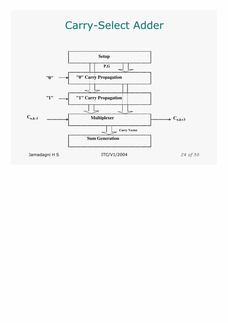
Carry-Select Adder
Setup
"0" Carry Propagation
"1" Carry Propagation
Multiplexer
Sum Generation
Co,k-1 Co,k+3
"0"
"1"
P,G
Carry Vector

5/17/2018 Learning Material - VLSI Design - slidepdf.com
http://slidepdf.com/reader/full/learning-material-vlsi-design 25/172
Jamadagni H S 2 5 o f 5 0 ITC/V1/2004
Carry Select Adder: Critical Path
Setup
"0" Carry
"1" Carry
Multiplexer
Sum Generation
"0"
"1"
Setup
"0" Carry
"1" Carry
Multiplexer
Sum Generation
"0"
"1"
Setup
"0" Carry
"1" Carry
Multiplexer
Sum Generation
"0"
"1"
Setup
"0" Carry
"1" Carry
Multiplexer
Sum Generation
"0"
"1"
Bit 0-3 Bit 4-7 Bit 8-11 Bit 12-15
S0-3 S4-7 S8-11 S12-15
Co,15Co,11Co,7Co,3Ci,0

5/17/2018 Learning Material - VLSI Design - slidepdf.com
http://slidepdf.com/reader/full/learning-material-vlsi-design 26/172
Jamadagni H S 2 6 o f 5 0 ITC/V1/2004
Linear Carry Select
Setup
"0" Carry
"1" Carry
Multiplexer
Sum Generation
"0"
"1"
Setup
"0" Carry
"1" Carry
Multiplexer
Sum Generation
"0"
"1"
Setup
"0" Carry
"1" Carry
Multiplexer
Sum Generation
"0"
"1"
Setup
"0" Carry
"1" Carry
Multiplexer
Sum Generation
"0"
"1"
Bit 0-3 Bit 4-7 Bit 8-11 Bit 12-15
S0-3 S4-7 S8-11 S12-15
Ci,0
(1)
(1)
(5)(6) (7) (8)
(9)
(10)
(5) (5) (5)(5)

5/17/2018 Learning Material - VLSI Design - slidepdf.com
http://slidepdf.com/reader/full/learning-material-vlsi-design 27/172
Jamadagni H S 2 7 o f 5 0 ITC/V1/2004
Square Root Carry Select
Setup
"0" Carry
"1" Carry
Multiplexer
Sum Generation
"0"
"1"
Setup
"0" Carry
"1" Carry
Multiplexer
Sum Generation
"0"
"1"
Setup
"0" Carry
"1" Carry
Multiplexer
Sum Generation
"0"
"1"
Setup
"0" Carry
"1" Carry
Multiplexer
Sum Generation
"0"
"1"
Bit 0-1 Bit 2-4 Bit 5-8 Bit 9-13
S0-1 S2-4 S5-8 S9-13
Ci,0
(4) (5) (6) (7)
(1)
(1)
(3) (4) (5) (6)
Mux
Sum
S14-19
(7)
(8)
Bit 14-19
(9)
(3)

5/17/2018 Learning Material - VLSI Design - slidepdf.com
http://slidepdf.com/reader/full/learning-material-vlsi-design 28/172
Jamadagni H S 2 8 o f 5 0 ITC/V1/2004
Adder Delays - Comparison
0.0 20.0 40.0 60.0
N
0.0
10.0
20.0
30.0
40.0
50.0
t p
ripple adder
linear select
square root select

5/17/2018 Learning Material - VLSI Design - slidepdf.com
http://slidepdf.com/reader/full/learning-material-vlsi-design 29/172
Jamadagni H S 2 9 o f 5 0 ITC/V1/2004
Look Ahead - Basic Idea
A0,B0 A1,B1 AN-1,BN-1...
Ci,0 P0 Ci ,1 P1Ci,N-1 PN-1
...

5/17/2018 Learning Material - VLSI Design - slidepdf.com
http://slidepdf.com/reader/full/learning-material-vlsi-design 30/172
Jamadagni H S 3 0 o f 5 0 ITC/V1/2004
Look-Ahead: Topology
VDD
P3
P2
P1
P0
G3
G2
G1
G0
Ci,0
Co,3

5/17/2018 Learning Material - VLSI Design - slidepdf.com
http://slidepdf.com/reader/full/learning-material-vlsi-design 31/172
Jamadagni H S 3 1 o f 5 0 ITC/V1/2004
Logarithmic Look-Ahead Adder
A7
F
A6A5A4A3A2A1
A0
A0A1
A2
A3
A4
A5
A6
A7
F
tp∼ log2(N)
tp∼ N

5/17/2018 Learning Material - VLSI Design - slidepdf.com
http://slidepdf.com/reader/full/learning-material-vlsi-design 32/172
Jamadagni H S 3 2 o f 5 0 ITC/V1/2004
Brent-Kung Adder
(G0,P0)
(G1
,P1
)
(G2,P2)
(G3,P3)
(G4,P4)
(G5,P5)
(G6,P6)(G7,P7)
C o,0
C o,1
C o,2
C o,3
C o,4
C o,5
C o,6
C o,7
tadd ∼ log2(N)

5/17/2018 Learning Material - VLSI Design - slidepdf.com
http://slidepdf.com/reader/full/learning-material-vlsi-design 33/172
Jamadagni H S3 3 o f 5 0
ITC/V1/2004
The Binary Multiplication
X··
Y× Zk2k
k 0=
M N 1–+
∑= =
Xi2i
i 0=
M 1–
∑⎝ ⎠⎜ ⎟⎜ ⎟⎜ ⎟⎛ ⎞
Y j2 j
j 0=
N 1–
∑⎝ ⎠⎜ ⎟⎜ ⎟⎜ ⎟⎛ ⎞
=
XiY j2i j+
j 0=
N 1–
∑⎝ ⎠⎜ ⎟⎜ ⎟⎜ ⎟⎛ ⎞
i 0=
M 1–
∑=
Xi2i
i 0=
M 1–
∑=
Y Y j2 j
j 0=
N 1–
∑=
with

5/17/2018 Learning Material - VLSI Design - slidepdf.com
http://slidepdf.com/reader/full/learning-material-vlsi-design 34/172
Jamadagni H S3 4 o f 5 0
ITC/V1/2004
The Binary Multiplication
1 0 1 1
1 0 1 0 1 0
0 0 0 0 0 0
1 0 1 0 1 0
1 0 1 0 1 0
1 0 1 0 1 0
×
1 1 1 0 0 1 1 1 0
+
Partial Products
AND operation

5/17/2018 Learning Material - VLSI Design - slidepdf.com
http://slidepdf.com/reader/full/learning-material-vlsi-design 35/172
Jamadagni H S3 5 o f 5 0
ITC/V1/2004
The Array Multiplier
HA FA FA HA
FA FA FA HA
FA FA FA HA
X0X1X2X3 Y1
X0X1X2X3 Y2
X0X1X2X3 Y3
Z1
Z2
Z3Z4Z5Z6
Z0
Z7

5/17/2018 Learning Material - VLSI Design - slidepdf.com
http://slidepdf.com/reader/full/learning-material-vlsi-design 36/172
Jamadagni H S3 6 o f 5 0
ITC/V1/2004
The MxN Array Multiplier
— Critical Path
HA FA FA HA
HAFAFAFA
FAFA FA HA
Critical Path 1
Critical Path 2
Critical Path 1 & 2

5/17/2018 Learning Material - VLSI Design - slidepdf.com
http://slidepdf.com/reader/full/learning-material-vlsi-design 37/172
Jamadagni H S3 7 o f 5 0
ITC/V1/2004
Carry-Save Multiplier
HA HA HA HA
FAFAFAHA
FAHA FA FA
FAHA FA HA
Vector Merging Adder

5/17/2018 Learning Material - VLSI Design - slidepdf.com
http://slidepdf.com/reader/full/learning-material-vlsi-design 38/172
Jamadagni H S3 8 o f 5 0
ITC/V1/2004
Adder Cells in Array Multiplier
A
B
P
Ci
VDDA
A A
VDD
Ci
A
P
AB
VDD
VDD
Ci
Ci
Co
S
Ci
P
P
P
P
P
Identical Delays for Carry and Sum

5/17/2018 Learning Material - VLSI Design - slidepdf.com
http://slidepdf.com/reader/full/learning-material-vlsi-design 39/172
Jamadagni H S3 9 o f 5 0
ITC/V1/2004
Multiplier Floorplan
SCSCSCSC
SCSCSCSC
SCSCSCSC
SC
SC
SC
SC
Z0
Z1
Z2
Z3Z4Z5Z6Z7
X0X1X2X3
Y1
Y2
Y3
Y0
Vector Merging Cell
HA Multiplier Cell
FA Multiplier Cell
X and Y signals are broadcasted
through the complete array.
( )

5/17/2018 Learning Material - VLSI Design - slidepdf.com
http://slidepdf.com/reader/full/learning-material-vlsi-design 40/172
Jamadagni H S4 0 o f 5 0
ITC/V1/2004
Wallace-Tree Multiplier
FA
FA
FA
FA
y0 y1 y2
y3
y4
y5
S
Ci-1
Ci-1
Ci-1
Ci
Ci
Ci
FA
y0 y1 y2
FA
y3 y4 y5
FA
FA
CC S
Ci-1
Ci-1
Ci-1
Ci
Ci
Ci

5/17/2018 Learning Material - VLSI Design - slidepdf.com
http://slidepdf.com/reader/full/learning-material-vlsi-design 41/172
Jamadagni H S4 1 o f 5 0
ITC/V1/2004
Multipliers —Summary
• Optimization Goals Different Vs Binary Adder
• Once Again: Identify Critical Path
• Other possible techniques
- Data encoding (Booth)- Pipelining
FIRST GLIMPSE AT SYSTEM LEVEL OPTIMIZATION
- Logarithmic versus Linear (Wallace Tree Mult)
f

5/17/2018 Learning Material - VLSI Design - slidepdf.com
http://slidepdf.com/reader/full/learning-material-vlsi-design 42/172
Jamadagni H S4 2 o f 5 0 ITC/V1/2004
The Binary Shifter
Ai
Ai-1
Bi
Bi-1
Right Leftnop
Bit-Slice i
...
Th B l Shif

5/17/2018 Learning Material - VLSI Design - slidepdf.com
http://slidepdf.com/reader/full/learning-material-vlsi-design 43/172
Jamadagni H S 4 3 o f 5 0 ITC/V1/2004
The Barrel Shifter
Sh3Sh2Sh1Sh0
Sh3
Sh2
Sh1
A3
A2
A1
A0
B3
B2
B1
B0
: Control Wire
: Data Wire
Area Dominated by Wiring
4 4 b l hift

5/17/2018 Learning Material - VLSI Design - slidepdf.com
http://slidepdf.com/reader/full/learning-material-vlsi-design 44/172
Jamadagni H S 4 4 o f 5 0 ITC/V1/2004
4x4 barrel shifter
BufferSh3S h2Sh 1Sh0
A3
A2
A 1
A 0
Widthbarrel ~ 2 pm M
L ith i Shift

5/17/2018 Learning Material - VLSI Design - slidepdf.com
http://slidepdf.com/reader/full/learning-material-vlsi-design 45/172
Jamadagni H S 4 5 o f 5 0 ITC/V1/2004
Logarithmic ShifterSh1 Sh1 Sh2 Sh2 Sh4 Sh4
A3
A2
A1
A0
B1
B0
B2
B3
0 7 bit L ith i Shift

5/17/2018 Learning Material - VLSI Design - slidepdf.com
http://slidepdf.com/reader/full/learning-material-vlsi-design 46/172
Jamadagni H S 4 6 o f 5 0 ITC/V1/2004
0-7 bit Logarithmic Shifter
Design as a T ade Off

5/17/2018 Learning Material - VLSI Design - slidepdf.com
http://slidepdf.com/reader/full/learning-material-vlsi-design 47/172
Jamadagni H S 4 7 o f 5 0 ITC/V1/2004
Design as a Trade-Off
0 10 20N
0.0
20.0
40.0
60.0
80.0
t
p
( n s e c )
0 10 20N
0.0
0.2
0.4
A
r e a ( m m
2 )
look-ahead
select
bypass
manchester
mirrorstatic
manchester
look-ahead
select
static
mirror
bypass
Layout Strategies for Bit-Sliced

5/17/2018 Learning Material - VLSI Design - slidepdf.com
http://slidepdf.com/reader/full/learning-material-vlsi-design 48/172
Jamadagni H S 4 8 o f 5 0 ITC/V1/2004
y gDatapaths
Well
ControlWires
(M1)
Well
Wires(M1)
GNDV DD
GND
GND
V DD
GND
Approach I —
Signal and power lines parallel
Approach II —
Signal and power lines perpendicular
S i g
n a l s W i r e s ( M 2 )
S i g n a l s W i r e s ( M 2 )
Layout of Bit sliced Datapaths

5/17/2018 Learning Material - VLSI Design - slidepdf.com
http://slidepdf.com/reader/full/learning-material-vlsi-design 49/172
Jamadagni H S 4 9 o f 5 0 ITC/V1/2004
Layout of Bit-sliced Datapaths
Layout of Bit sliced Datapaths

5/17/2018 Learning Material - VLSI Design - slidepdf.com
http://slidepdf.com/reader/full/learning-material-vlsi-design 50/172
Jamadagni H S 5 0 o f 5 0 ITC/V1/2004
Layout of Bit-sliced Datapaths
(a) Datapath without feedthroughs
and without pitch matching
(area = 4.2 mm2).
(b) Adding feedthroughs
(area = 3.2 mm2)
(c) Equalizing the cell height reduces
the area to 2.2 mm2.
Information Theory and Coding Chapter 1
C

5/17/2018 Learning Material - VLSI Design - slidepdf.com
http://slidepdf.com/reader/full/learning-material-vlsi-design 51/172
1 . I NTRODUCTI ON TO LOW POW ER VLSI
Power consumption, speed of operation, and silicon area occupied are the most
important attributes of integrated circuit implementation of electronic circuits. Mostintegrated circuit designs focus on these issues and try to optimize one or more of
these attributes. Of these, low power consumption is becoming the most important as
markets for portable, handheld equipment is growing. Also, new generations of semiconductor processing technologies need to reduce power dissipation of digital
circuits due to large device density and higher operating speed.
Analysis of power consumption and its optimization has been traditionally carried out
for analog circuit design. It is now becoming important in the digital design influencing
all aspects of the design.
Power is the rate at which energy is delivered or exchanged. In a VLSI, electrical
energy is converted to thermal energy during the operation of the circuit. Power
dissipated by a circuit is the rate at which energy is taken from the source minus therate at which energy delivered by the circuit to a load. The energy converted to heat is
removed from the chip for maintaining a reasonable temperature of the semiconductorsubstrate.
Low power circuit design for VLSI includes analysis of power dissipation in the circuitand its optimization. In analysis we try to estimate the power or energy dissipation at
different phases of the design process. Its purpose is to increase confidence of thedesign with the assurance that the power consumption specifications are not violated.
Accuracy of analysis depends on the availability of design information. In early phasesof design, we attempt to get power dissipation estimates using only the system model
of the circuit to be designed as we don’t have much information on the detailed design.Therefore, in this phase results obtained are not accurate. However, it helps us to take
an appropriate approach to circuit design for low power. As the design proceeds to
gate, and circuit level, a more accurate analysis is carried out. These analyses producemore accurate estimates but take longer computation time.
Analysis techniques also form the basis for design optimization. Optimization is the
process of generating the best design, given an optimization goal, without violating
design specifications. An automatic design optimization algorithm requires fast analysisto evaluate the merits of the design choices. Manual optimization also demands a
reliable analysis tool to provide accurate estimation of power dissipation. A decision toapply a particular low power technique often involves trade-offs from conflicting
requirements. In such contexts, main criteria to be considered are the impact on thecircuit delay, and the chip area. Other factors of chip design such as design cycle time,
testability, quality, reliability, reusability, and risk may be affected by a particular
design decision to achieve the low power.
1 .1 . Need f o r Low Pow er VLSI
Information Theory and Coding Chapter 1
experienced a rapid density growth compared to VLSI circuits Stored energy per unit

5/17/2018 Learning Material - VLSI Design - slidepdf.com
http://slidepdf.com/reader/full/learning-material-vlsi-design 52/172
experienced a rapid density growth compared to VLSI circuits. Stored energy per unit
Information Theory and Coding Chapter 1
weight of batteries roughly doubles in about a decade Therefore the battery

5/17/2018 Learning Material - VLSI Design - slidepdf.com
http://slidepdf.com/reader/full/learning-material-vlsi-design 53/172
weight of batteries roughly doubles in about a decade. Therefore, the battery
technology alone will not solve the low power problem in the near future.
The power dissipation of high performance microprocessors could be several tens of
Watts and CPUs in some personal computers require cooling fans directly mounted onthe chip due to this power dissipation. A chip that operates at 3V, consuming 10W of
power draws an average current of 3A. The transient current could be as high as 10A.This creates problem in the design of power supply rails and poses big challenges in
the assuring adequate noise immunity.
With a push towards generation and use of “clean energy”, it has also become
necessary to save power usage to extent possible. In fact power saving is analternative strategy to generate more power. Since electricity generation is a major
source of pollution, inefficient energy usage in computing equipment indirectlycontributes to environmental pollution. With promotion of energy compliance forelectronic equipment in various countries, low power design assumes a central position
in saving power in these equipment.
1 .2 . Mechan isms o f pow er d iss ipa t ion in VLSI
There are two types of power dissipation in CMOS circuits: dynamic and static.
• Dynamic power dissipation is mainly due to charging of load capacitances duringswitching activities of the circuits. A higher operating frequency leads to more
frequent switching activities in the circuits and results in increased powerdissipation. A second cause of dynamic dissipation is due to short circuit current that
flows between the supply and ground rails of the CMOS circuit for a brief period
during switching when the CMOS elements between these rails are both on.• In CMOS logic, leakage current is the source of static power dissipation. This current
flows from the supply rail to the ground rail as a DC due to the device which isexpected to be off conducting a leakage current due to several effects present in a
MOS device. Also, deviations from the CMOS style logic can cause additional staticcurrent to be drawn.
The most dominant source of dynamic power dissipation in CMOS circuits is thecharging and discharging of load capacitances. Most digital CMOS circuits do not
require capacitors for their intended operations. The capacitances are found in circuits
due to parasitic effects of interconnection wires and transistors. Such parasiticcapacitances cannot be avoided and it has a significant impact on the power
dissipation of the circuits. The estimation and analysis of parasitic capacitance iscrucial for estimating power as well as signal delays.
Figure 1.1 shows the equivalent circuit of charging and discharging output capacitance
of a CMOS logic gate. We use a toggling switch to model the charging and discharging
cycles.
Information Theory and Coding Chapter 1
Fig 1 1: Capacitance charging and discharging in a CMOS circuit

5/17/2018 Learning Material - VLSI Design - slidepdf.com
http://slidepdf.com/reader/full/learning-material-vlsi-design 54/172
Fig 1.1: Capacitance charging and discharging in a CMOS circuit
In fig 1.1 V is an ideal constant voltage source and R c and Rd are charging anddischarging resistances of circuit respectively. The voltage vc(t) and the current ic(t) of
a capacitance C L at time t are given by
cc L
dv (t)i (t) C
dt= (1.1)
During the charging cycle from time t0 to t1, the energy Es drawn from the voltagesource is
1
0
t
s ctE V i (t) dt= • •∫ (1.2)
Initially the capacitor contains no charge and the voltage across its terminals is zero,
that is, vc(t0) = 0. Assuming that the capacitor is fully charged at the end of thecharging cycle, we have vc(t1) = V. Substituting Equation (1.1) into (1.2), we have
( )1 1
0 0
t t
2cs L L c L
t t
dv (t)E C V dt C V dv C V
dt
⎛ ⎞= • = • = •⎜ ⎟
⎝ ⎠∫ ∫ (1.3)
Part of the electrical energy E s drawn from the voltage source is stored in the capacitorand the rest is dissipated in the resistor R c. The energy E c stored in the capacitor at the
end of the charging cycle is
1 1
0 0
t t V2c
c c c L c L c c L
t t 0
dv (t) 1E v (t) i (t) dt C v (t) dt C v (t) dv C V
dt 2= = = =∫ ∫ ∫ (1.4)
From Equations (1.3) and (1.4), the energy dissipated in R c during charging is
therefore
2
R s c L
1E E E C V
2= − = (1.5)
Now consider the discharging cycle from t1 to t2, we assume that the capacitor is fullydischarged, that is, vc(t1) = V and vc(t2) = 0. The energy E d dissipated in the discharge
resistor R d is
2
1
t 02
d c c L c c L
t V
1E v (t) i (t) dt C v (t) dv C V
2= − = − =∫ ∫ (1.6)
E d is equal to the energy stored in the capacitance at the beginning of the dischargingcycle. If we charge and discharge the capacitance at the frequency of f cycles per
Information Theory and Coding Chapter 1
We observe that during charging, CLV2 energy is drawn from the energy source, half of

5/17/2018 Learning Material - VLSI Design - slidepdf.com
http://slidepdf.com/reader/full/learning-material-vlsi-design 55/172
g g g, CL gy gy ,
which is dissipated in the charging resistance R c and the other half is stored in thecapacitor. During discharge, the energy stored in the capacitor is dissipated in the
discharging resistor R d. Assumptions in the above calculations are:
• CL is constant
• V is constant• CL is fully charged and discharged respectively at t0and t2.
The result is independent of the charging and discharging circuit resistances (Rc, Rd), length of charging, discharging cycle (t0, t1, t2), and the voltage or current waveforms
vc(t), ic(t). Moreover, Rc, Rd can be nonlinear, and time varying. The equation 1.7 is
valid as long as the above three assumptions are satisfied. Most CMOS digital circuitsdesigned today satisfy the above assumptions during logic operations. Therefore, for
most CMOS circuits operating at medium to high frequency, this is the dominant modeof power dissipation. Equation (1.7) is only the power dissipation caused by a single
capacitor CL. In general, the total power should be summed over each capacitance C i in a circuit giving the following equation.
2
i i ii
P C V f = ∑ (1.8)
Here Vi is the voltage swing across the capacitor Ci switching at frequency f i. For CMOS
circuits, V is typically the same for all capacitance Ci. If we further assume that f i isconstant, (for example, by taking the average of all f i’s) we get
2 2
i totali
P V f C C V f = =∑ (1.9)
Here Ctotal is the sum of all capacitance, f is the average frequency and V is the voltage
swing.
In today’s typical CMOS process with minimum feature size of 90 to 180 nm, typicalvalues of Ci are in the order of 1fF to 1pF, charging and discharging frequency several
hundred MHz, with V of 1 to 3V.
1 .2 .1 . Example
A 16 bit bus operating at 3.3 V and 100 MHz clock rate is driving a capacitance of 20
pF/bit. Each bit has a toggling probability of 0.25 at each clock cycle. What is the
power dissipation in operating the bus?
C = 16 x 20 = 320 pF
V = 3.3 V
Information Theory and Coding Chapter 1
Figure 1.2 shows a CMOS inverter with transistor threshold voltages of Vtn and Vtp as

5/17/2018 Learning Material - VLSI Design - slidepdf.com
http://slidepdf.com/reader/full/learning-material-vlsi-design 56/172
g g p
shown on the transfer curve. When the input signal level is above V tn, the N-transistoris on. Similarly, when the signal level is below Vtp, the P-transistor is on. When the
input signal vi switches, there is a short duration during which the input level is
between Vtn and Vtp and both transistors are turned on. This causes a short circuitcurrent from Vdd to ground that dissipates power.
Figure 1.3 shows the approximate current waveforms during the transition. The
current is zero when the input signal is below Vtn or above Vtp. The current increases
as vi rises beyond Vtn and decreases as it approaches Vtp. Integration of the currentover time multiplied by the supply voltage is the energy dissipated during the input
transition period.
The shape of the short circuit current is dependent on the duration and slope of theinput signal, the transfer characteristics of the P and N transistors (which in turn
depend on their sizes, process technology, temperature, etc), and the output loading
capacitance of the inverter.
Fig.1.2 Inverter and its characteristics
Assuming the input to be ramp signal, an analysis of the short circuit current shows
that the energy dissipated is
( )2
short tp tnE V V
12
β= • τ • − (1.10)
Here β is dependent on the size transistors and τ is the rising duration of the input
signal. This equation is useful in only indicative of the relationship of variousparameters to the short circuit energy and power dissipation. In practical circuitsenergy dissipation is a more complex function of the parameters shown in equation
1.10. The equation also assumes that the output loading capacitance of the CMOS
inverter is zero which is not true in real circuits.
Information Theory and Coding Chapter 1
1.3: Short circuit current in an Inverter

5/17/2018 Learning Material - VLSI Design - slidepdf.com
http://slidepdf.com/reader/full/learning-material-vlsi-design 57/172
However, the short circuit dissipation can be found accurately using circuit simulatorssuch as SPICE. To obtain the short circuit current when the inverter input changes
from low to high, we measure the source-drain current of the N-transistor.
1 .3 .2 . Sh o r t c i r cu i t cu r re n t va r i a t i o n w i t h o u tp u t l o ad
Short circuit current magnitude and the shape varies with respect to the output
loading capacitance and the input signal slope of a CMOS inverter. Thesecharacteristics of the short circuit current have some implications on the analysis and
optimization of the power efficiency for CMOS circuits. We have observed that duration
of short circuit current depends on the transition period of the input signal. The short
circuit current has also been known to depend on the output loading capacitance.
Consider the case when the input voltage is falling and the output voltage is rising.
Based on the on-off properties of the transistors, the short circuit current is non-zeroonly when the input level is between Vtn and Vtp. When the inverter input is at Vdd /2,
its output voltage is between 0 and Vdd /2 assuming a symmetrical transfer curve. If
the output capacitance is large, the output voltage is nearly zero and the voltageacross the source and drain of the N-transistor is only slightly above zero. The low
source-drain potential difference results in small short circuit current. Conversely, if
the output capacitance is small, the output voltage rises faster and the source-drainvoltage is much higher, causing a larger short circuit current.
It can be shown (typically by SPICE simulation) that the short circuit current envelope
is the largest when the output capacitance is the smallest. As the output capacitanceincreases, the current envelope becomes. The duration of the short circuit current is
independent of the output capacitance because it depends on the input signal slopeonly. The short circuit current is non-zero only when the input voltage is between Vtn
and Vtp. Therefore, increasing the output loading capacitance reduces the short circuit
energy per transition, for the same input signal conditions.
This means that increasing the output capacitance decreases the short circuit powerdissipation. However, the dynamic dissipation increases as the dissipation component
due to increased load capacitance increases. Therefore, low power digital design
should always try to reduce load capacitances. A major contribution to this is the inputcapacitance of the gate receiving the signal. The size of the receiving gate is
constrained by its speed requirement and driving a signal faster than necessary resultsin wasted power. Thus for low power design, a good design practice is to choose the
minimum gate size that meets the speed constraint to minimize capacitance. Thisagrees with the minimum area design goal and presents no conflicting requirements in
the area-power trade-off.
1 .3 .3 . Shor t c i rcu i t Cur r en t Var ia t ion w i th I npu t S igna l Slope
Information Theory and Coding Chapter 1
Therefore, to reduce power dissipation of a CMOS circuit, we should use the fastest

5/17/2018 Learning Material - VLSI Design - slidepdf.com
http://slidepdf.com/reader/full/learning-material-vlsi-design 58/172
input signal slope for all signals. However, while the fast signal reduces powerdissipation of the signal receiving gate, the transistor sizes of the signal driving gate
have to be increased to sustain the steep slope. A larger driver gate means more
power consumption due to increased input capacitance and short circuit current. Thus,sharp signal slopes presents conflicting effects on the power dissipation of the signal
driver and receiver gates. A rule-of-thumb used as a compromise is the duration of theinput signal (say, as measured from 10% to 90% voltage) should be comparable to
the propagation delay of the gate.
1 .4 . St a t i c pow er d i s s ipa t i on and l eak age Cu r r en t
Static power dissipation in a CMOS circuit is due to the leakage current, which is dueto a phenomenon of the semiconductor device operation. In circuits that use MOS
transistors, there are two major sources of leakage current: 1. reverse biased PN-
junction current and, 2. subthreshold channel conduction current.
1 .4 .1 . Reverse Biased PN- j unct ion
This source of leakage current occurs when the source or drain of an N-transistor (P-
transistor) is at Vdd (Vss). PN-junctions are formed at the source or drain of transistorsbecause of a parasitic effect of the bulk CMOS device structure. As shown in Figure
1.7, the junction current at the source or drain of the transistor is picked up throughthe bulk or well contact. The magnitude of the current depends on the temperature,
process, bias voltage and the area of the PN-junction. The reverse biased PN-junctioncurrent is
r s
th
VI I exp 1
V
⎡ ⎤⎛ ⎞= −⎢ ⎥⎜ ⎟
⎢ ⎥⎝ ⎠⎣ ⎦(1.11)
Is is the reverse saturation current dependent on the fabrication process and the PN- junction area. Vth is the therm al voltage where
th
kTV
q= (1.12)
In the above equation, k is the Boltzmann’s constant, q is the electronic charge and T
is the device operating temperature. At room temperature, T = 300K and Vth =25.9mV.
In equation (1.11) V is negative as the PN-junction is in reversed bias. If |V| >>Vth, wehave eV/Vth is nearly 0 and Ir = - Is. Thus, a small reverse voltage is sufficient to induce
current saturation. For all practical purposes, the current is independent of the circuitoperating voltage.
Information Theory and Coding Chapter 1
becoming significant in recent 90 nm technology. For future technologies like the 65
d l th l k t ill b i ifi t F t h l i ith

5/17/2018 Learning Material - VLSI Design - slidepdf.com
http://slidepdf.com/reader/full/learning-material-vlsi-design 59/172
nm and lower, the leakage current will become very significant. For technologies withlarger feature size, this component is negligible at usual operating temperature of the
chip.
1 .4 .2 . Subth resho ld cu r r en t
The second source of leakage current is the subthreshold leakage through a MOSdevice channel. Even though a transistor is logically turned off, there is a non-zero
leakage current through the channel, as illustrated in Figure 1.5. This current is knownas the subthreshold leakage because it occurs when the gate voltage is below its
threshold voltage.
Fig 1.5 Subthreshold current in a MOS transistor
The subthreshold conduction current Isub depends on the device dimension, fabrication
process, gate voltage Vgs, drain voltage Vds and temperature. The dependency on Vds isinsignificant if it is much larger the thermal voltage. In CMOS circuits subthreshold
current occurs when Vds = Vdd and therefore, the current depends mainly on Vgs, devicedimension and operating temperature. Subthreshold conduction current is given by
gs t
sub 0
th
V V
I I exp V
−⎛ ⎞
= ⎜ ⎟α⎝ ⎠ (1.13)
Where Vt is the device threshold voltage, Vth is the thermal voltage (25.9mV at room
temperature), and I0 is the current when Vgs = Vt. The parameter α is a constant
depending on the device fabrication process, ranging from 1.0 to 2.5. The expression
(Vgs– Vt) has a negative value so that Isub drops exponentially as Vgs decreases.
A typical plot of Isub with Vgs of a MOS transistor is illustrated in Figure 1.6. The slope
at which Isub decreases is an important parameter in low power design. By taking thelogarithm and differentiation of Equation (1.13), the slope can be expressed as
Information Theory and Coding Chapter 1

5/17/2018 Learning Material - VLSI Design - slidepdf.com
http://slidepdf.com/reader/full/learning-material-vlsi-design 60/172
Fig 1.6 Subthreshold current Vs Vgs
( )gs th
sub
V V kT2.3
logI loge q
∆ α= = α
∆ (1.14)
At room temperature with Vth = 25.9mV, the slope ranges from an ideal 60mV/decadeto 150m V/decade. A smaller value is desirable because the decrease in subthreshold
per unit changes in gate voltage Vgs is larger. The slope flattens as the temperature T
rises.
Subthreshold conduction current is becoming a limiting factor in low voltage and lowpower chip design. When the operating voltage is reduced, the device threshold
voltage Vt has also to be reduced to compensate for the loss in switching speed.
Consider a conventional CMOS circuit operating at Vdd = 5 V and Vt = 0.9V. Assumingan ideal slope of 60mV/decade in equation (1.14), the subthreshold current is about
900/60 = 15 decades smaller from Vgs = Vt to Vgs = 0. Such low leakage is negligible.However, in a low power design with Vdd = 1.2V, Vt = 0.45V only 450/60 = 7.5 orders
of magnitude increase in subthreshold conduction current as compared to the highvoltage device. The problem is worsened at high temperature 125 degree Celsius as
the slope becomes 80mV/decade and the subthreshold conduction current coulddeteriorate to 450/80 = 5.6 decades. Decreasing subthreshold current is an important
factor in low power design.
1 .4 .3 . Su m m a ry o n l e a ka g e cu r re n t
Subthreshold leakage and reverse-biased junction leakage have very similar
characteristics. They are both in the order of pico-Ampere per device and very
sensitive to process variation. Both increase dramatically with temperature and arerelatively independent of operating voltage for a given fabrication process. Although
the leakage current cannot be ignored in low power circuit design, the logic or circuitdesigns do not pay any special attention to reduce this current. Leakage current is
difficult to predict, measure, or optimize. Most high performance digital circuits
Information Theory and Coding Chapter 1
The pseudo NMOS circuit does not require a P-transistor network and saves half the
transistors required for logic computation as compared to the CMOS logic The circuit

5/17/2018 Learning Material - VLSI Design - slidepdf.com
http://slidepdf.com/reader/full/learning-material-vlsi-design 61/172
transistors required for logic computation as compared to the CMOS logic. The circuithas a property that the current only flows when the output is at logic 0. When the
output is at logic 1, all N-transistors are off and no static current flows except for the
leakage current. This property may be exploited in a low power design. If a signal isknown to have very high probability of logic 1 it may be better to implement pseudo
NMOS logic. Also, if the signal probability is very close to zero, we may replace theNMOS logic with a load transistor of N type.
1 .6 . Pr inc ip les o f Low Pow er Des ign
Analysis of power dissipation mechanisms in Silicon ICs leads us to the following basic
mechanisms of low power design.
1 .6 .1 . Sw i tch ing and supp ly vo l tage reduct ion
The dynamic power of digital chips expressed by Equation (1.8) is the largest portion
of power dissipation. Due to the quadratic effect of the voltage term, reducing theswitching voltage can achieve significant power savings. The easiest method to achieve
this is to reduce the operating voltage of the CMOS circuit. Other methods reduce
voltage swing by using well-known circuit techniques such as charge sharing,transistor threshold voltage. There are many trade-offs to be considered in supply
voltage reduction. MOS transistors become slower at lower operating voltages as thethreshold voltages of the transistors do not scale the operating voltage. Noise
immunity is also reduced at low voltage swing.
1 .6 .2 . Capaci tance reduct ion
Reducing parasitic capacitance in is a good way to improve performance as well as
reduce power. However, the real goal is to reduce the product of capacitance and itsswitching frequency. Signals with high switching frequency should be routed with
minimum parasitic capacitance to conserve power. Conversely, nodes with largeparasitic capacitance should not be allowed to switch at high frequency. Capacitance
reduction can be achieved at many design abstraction levels: material, process
technology, physical design (floor planning, placement and routing), circuit techniques,transistor sizing, logic restructuring, architecture transformation, and alternative
computation algorithms.
1 .6 .3 . Swi tch ing f requency reduct ion
Reducing switching frequency has the same effect as reducing capacitance. Again,frequency reduction is best applied to signals with large capacitance. The techniquesare often applied to logic level design and above. Those applied at a higher abstraction
level generally have greater impact. Reduction of switching frequency also has the sideeffect of improving the reliability of a chip as some failure mechanism is related to the
switching frequency An effective method of reducing switching frequency is to
Information Theory and Coding Chapter 1
Leakage current is not useful in digital circuits. However, we often have very little
control over the leakage current as it is technology dependent In technologies with

5/17/2018 Learning Material - VLSI Design - slidepdf.com
http://slidepdf.com/reader/full/learning-material-vlsi-design 62/172
control over the leakage current as it is technology dependent. In technologies withlarge feature size (say, above 130 nm) the leakage power dissipation of a CMOS digital
circuit is several orders of magnitude smaller than the dynamic power. The leakage
power dominates in very low frequency circuits or circuits with “sleep modes” wheredynamic activities are suppressed. Most leakage reduction techniques are applied at
low-level design abstraction such as process, device, and circuit design. Memories thathave very high device density are most susceptible to high leakage power.
Static current can be reduced by transistor sizing, layout techniques and careful circuitdesign. Circuit modules that consume static current could be turned off if not used.
Sometimes, static current depends on the logic state of its output and we can considerreversing the signal polarity to minimize the probability of static current flow.
We note that no single low power technique is applicable to all situations. Design
constraints should be viewed from all angles within the bounds of the design
specification. Low power considerations should be applied at all levels of designabstraction and design activities. Chip area and speed are the major trade-off
considerations but a low power design decision also affects other aspects such asreliability, design cycle time, reusability, testability and design complexity. Early
design decisions have higher impact to the final results and therefore, power analysisshould be initiated early in the design cycle.
1 .7 . Fi g u r e o f m e r i t f o r l o w p o w e r c ir c u it s
The simplest unit of measure of a low power circuit is the power consumption. This
measure is useful for packaging considerations, system power supply and coolingrequirements. Also the peak power is used for power ground wiring design, signal
noise margin and reliability analysis.
An IC that operating at a higher frequency will consume more power. Since power is
the rate at which energy is consumed over time, the measure of energy in the unit of Joule becomes another choice of measure, expressed often in nW/MHz. Lower this
number, lower the power consumed to perform a given function at a given frequency.
However, when comparing two processors with different instruction sets or
architecture, this measure may be misleading. Different processors require differentnumber of clock cycles for the same instructions. A more objective measure in such a
case is nW/MIPS or mA/MIPS. Normalizing power dissipation with respect to MIPSallows us to compare processors with widely different performance rating. The
nW/MIPS measure has a unit of Watt-Second per Instruction. Thus, it is a measure of the energy consumed by a typical instruction. This figure of merit is useful when
comparing power efficiency of processors with similar instruction sets, for example,
two DSP processors of the same family. Because of the normalization, this measure isindependent of the performance or clock rate of the processor.
Information Theory and Coding Chapter 1
is a measure of computation speed derived from executing some standard benchmark
software programs written in machine independent high-level programming language.

5/17/2018 Learning Material - VLSI Design - slidepdf.com
http://slidepdf.com/reader/full/learning-material-vlsi-design 63/172
p g p g p g g g g
Other measures such as the energy delay product are commonly used to assess the
merits of a logic style. When battery life is of concern in portable electronicsapplications, we often define measures that involve the battery lifetime. Commercial
batteries are most often rated with mA-Hour, which is a unit of stored energy whenthe operating voltage is constant.
The choice of the figure of merit depends on the type of analysis and application area.No single measure is necessary for a particular situation nor is it sufficient for all
purposes. It is the designer’s responsibility to define the appropriate measures forpower analysis and optimization.
VLSI Design Test Problems
Test Problems:

5/17/2018 Learning Material - VLSI Design - slidepdf.com
http://slidepdf.com/reader/full/learning-material-vlsi-design 64/172
1. Design a CMOS transistor circuit to realize the Boolean function Y= A (B+C).
a. Simulate the circuit to measure power for input signal probabilities of 0.5 each. Vary the signal probabilities (say 0.3, 0.6, 0.8 etc) and
repeat the power measurement.b. Restructure (input reordering) the transistors and repeat part (a)
2. Design an inverter chain, which drives a large capacitive load (C load ) foroptimum delay, area, and power requirements. Determine the number of
stages (N) required for optimum delay case. Draw Pd Vs K (stage ratio).Assume Cload = 1pF and the gate capacitance of a min. sized inverter C0 =
26fF.
3.
Design single and double edge-triggered flip-flops and find Pd in each caseand compare them.
4. Design a four-bit asynchronous counter and measure the power dissipation asa function of frequency. Run this counter with half swing clock and measure
the power dissipation and compare this with the earlier case.5. Design a synchronous 4-bit counter and measure the power. Compare this
with the measurements of problem 4. Compare this power with the oneobtained with MSB switched off (i.e., when MSB is not in use = > clock to last
FF disabled). Measure the power saving.
Information Theory and Coding Chapter 2
Chapter 2 SI MULATI ON POWER ANALYSI S

5/17/2018 Learning Material - VLSI Design - slidepdf.com
http://slidepdf.com/reader/full/learning-material-vlsi-design 65/172
Computer simulation has been applied to VLSI design for several decades. Mostsimulation programs operate on mathematical models which mimic the physical laws andproperties of the object under simulation. Today, simulation is used for functionalverification, performance, cost, reliability and power analysis. Many simulation languages
have been developed specifically for IC’s. For example in digital logic simulation, VHDL(Very High Speed IC Hardware Description Language) and Verilog are two popularlanguages being used. Special purpose hardware has also been developed to speed upthe simulation process.
Simulation-based power estimation and analysis techniques have been developed andapplied to the VLSI design process [2.1] [2.3] [2.3] [2.4] [2.5] [2.6]. Simulation softwareoperating at various levels of design abstraction is a key technology in the mainstream VLSI design. The main difference between simulation at different levels of designabstraction is the trade-off between computing resources (memory and CPU time) andaccuracy of the results [2.7]. In general, simulation at a lower-level design abstractionoffers better accuracy at the expense of increased computer resource. Circuit simulators
such as SPICE attain excellent accuracy but cannot be applied to full-chip analysis. Logicsimulation generally can handle full-chip analysis but the accuracy is not as good andsometimes the execution speed is too slow. Behavioural-level or functional-levelsimulation offers rapid analysis but the accuracy is sacrificed. Figure 2.1 summarizes thetrade-off between computing resources and analysis accuracy at different levels of designabstraction.
Fig. 2.1
Since no single simulation technique is applicable to all levels of design, the top-downestimation, refinement and verification methodology is used. As an example, the designermay start with a simulation at the hardware behaviour level to obtain an initial powerdissipation estimate. When the gate-level design is available, a gate-level simulation isperformed to refine the initial estimate. If the initial estimate turns out to be inaccurateand the design fails the specification, the design is modified and verified again. Theiteration continues until the gate-level estimate is within specification. The design is then
taken to the transistor or circuit-level analysis to further verify the gate-level estimates.The refinement and verification steps continue until the completion of the design process,when the chip is suitable for mass production.
This chapter is dedicated to simulation techniques to estimate and analyze powerdi i i f CLSI hi Th i l i d di h f ili d i
Information Theory and Coding Chapter 2
2.1 SPI CE Circuit Sim ulat ion

5/17/2018 Learning Material - VLSI Design - slidepdf.com
http://slidepdf.com/reader/full/learning-material-vlsi-design 66/172
SPICE (Simulation Program with IC Emphasis) is the de facto power analysis tool at the
circuit level. A wealth of literature has already been dedicated to SPICE and dozens of SPICE-like application software packages are available today. We will only briefly discussits application to power analysis, assuming that the readers are already familiar withSPICE.
2.1 .1 SPI CE Basics
SPICE operates by solving a large matrix of nodal current using the Krichoff’s Current Law
(KCL). The basic components of SPICE are the primitive elements of circuit theory suchas resistors, capacitors, inductors, current sources and voltage sources. More complexdevice models such as diodes and transistors are constructed from the basic components.
The device models are subsequently used to construct a circuit for simulation. Basiccircuit parameters such as voltage, current, charge, etc., are reported by SPICE with ahigh degree of precision. Hence the circuit power dissipation can be directly derived fromSPICE simulation.
SPICE offers several analysis modes but the most useful mode for digital IC poweranalysis is called transient analysis . The analysis involves solving the DC solution of the
circuit at time zero and makes small time increments to simulate the dynamic behaviour of the circuit over time. Precise waveforms of the circuit parameters can be plotted over thesimulation time.
SPICE device models are derived from a characterization process. Each device model isdescribed by dozens of parameters. The models are typically calibrated with physical
measurements taken from actual test chips and can achieve a very high degree of accuracy. Lower-level analysis tools using Finite Element Methods or other physicalsimulation can also be used to produce the device model parameters.
2.1.1 SPI CE Pow er Analysis
The strongest advantage of SPICE is of cause its accuracy. SPICE is perhaps the mostversatile among all power analysis tools. It can be used to estimate dynamic, static and
leakage power dissipation. MOS and bipolar transistor models are typically available and italso faithfully captures many low-level phenomena such as charge sharing, cross talk andtransistor body effect. In addition, it can handle common circuit components such asdiodes, resistors, inductors and capacitors. Specialized circuit components can often bebuilt using the SPICE’s modeling capability.
Information Theory and Coding Chapter 2
problem is to apply extreme case analysis. Several sets of device models are generated torepresent the typical and extreme conditions of the chip fabrication process and operating

5/17/2018 Learning Material - VLSI Design - slidepdf.com
http://slidepdf.com/reader/full/learning-material-vlsi-design 67/172
environment. The conditions are generally defined by the speed of the device so that thedevice so that the designer can predict the fastest and slowest operating extremes of thecircuit. For example, most chip designers will simulate SPICE with three sets of parameters, TYPICAL, BEST and WORST case conditions based on the device speed.
The variation of semiconductor process could be large. The BEST and WORST case devicespeed could be 2X apart. The process variation of power dissipation is less but is still onthe same order. For most circuits using conventional CMOS processes, faster devicemodels generally correspond to higher power dissipation and vice versa. However, thereare exceptions : for example, a low-speed worst case device model may cause slow signalslopes with high short-circuit power. For designs with marginal power d\budget, theanalysis should be performed on some or all extreme cases to ensure specificationcompliance. The process variation problem affects all types of power and timing analysisusing the bottom-up characterization approach. With SPICE, the problem is more severedue to the accuracy sought at this level of analysis.
2.2 Discrete Transistor Modeling and Analysis
In SPICE, a transistor is modeled with a set of basic components using mathematicalequations. The solution of the node currents and voltages requires complex numericalanalysis involving matrix operations. Equation (2.1) gives a simple SPICE transistor modelto compute Ids as a function of Vgs and Vds. The model is obtained by the first orderapproximation of the nonlinear equation at the operating point Vgso and Vr
(2.1)
to form a linear approximation equation. In the small signal model, the equation can besimplified as
(2.2)
which leads to the model shown in Figure 2.2. The linear equation has to be numericallyevaluated in SPICE whenever the operating point Vgso and Vdso changes, resulting inexcessive computation requirements.
Fig. 2.2
Information Theory and Coding Chapter 2
computation, it applies the event-driven approach, in which an event is registered when asignificant change in node voltage occurs. If the event-driven approach fails, it rolls back t th i it l i th d A t i t l i th d i il t SPICE i d t

5/17/2018 Learning Material - VLSI Design - slidepdf.com
http://slidepdf.com/reader/full/learning-material-vlsi-design 68/172
to the circuit analysis method. A transient analysis method similar to SPICE is used toperform time step simulation. A notorious problem in simulating large circuits with SPICEis the DC convergence problem. Bulk of the simulation time is often attributed to find theinitial DC solution of the circuit so that it converges to a legal state. By using theknowledge that the circuit is mainly digital, the logic values from the primary inputs can bepropagated to the circuit to help solve the DC convergence problem.
The transistor model quantization process introduces inaccuracies but improves the speedof analysis. The maximum circuit size and analysis speed using the tabular transistormodel improves nearly two orders of magnitude compared to SPICE. The accuracy loss ismostly tolerable for digital circuits. Even with the increased capacity. Transistor-level toolsare often not able to perform full-chip power analysis of very large scale chips. Theanalysis speed is still several orders of magnitude slower than logic-level simulation. Chipswith up to a hundred thousand transistors can be handled by transistor-level tools bytmany VLSI chips today exceed that scale.
2.2.2 Sw it ch Level Analysis
Most digital circuit analysis is restricted to several basic circuit components such astransistors, capacitors and resistors. Because of the restricted component types,computation speed and memory can be improved by using higher-level abstraction modelwith little loss in accuracy. One such analysis is called switch-level simulation.
The basic idea of the switch-level simulation is to view a transistor as a two-state on-off switch with a resistor, as shown in Figure 2.2. A transistor is turned on when its gatevoltage exceeds the threshold voltage. Under this model, timing simulation can be
performed using approximated RC calculation that is more efficient than transistor modelanalysis.
Simulation tools for switch-level timing analysis have been reported [2.9] [2.10].Recently, power analysis tools based on these simulators have also been developed. Thepower dissipation is estimated from the switching frequency and capacitance of eachnode. Short-circuit power can also be accounted by observing the time in which theswitches form a power-ground path. The accuracy of switch-level analysis is worse than
circuit-level analysis but offers faster speed.
2.3 Gate-level Logic Sim ualt ion
Si l ti b d t l l ti i l i h b t t h i i t d ’
Information Theory and Coding Chapter 2
simulation time point. As one switching event occurs at the input of a logic gate, it maytrigger other events at the output of the gate after a specified time delay. Computersim lation of s ch e ents p o ides a e acc ate p e fab ication logic anal sis and

5/17/2018 Learning Material - VLSI Design - slidepdf.com
http://slidepdf.com/reader/full/learning-material-vlsi-design 69/172
simulation of such events provides a very accurate pre-fabrication logic analysis andverification of digital chips. Most gate-level simulation also supports other logic statessuch as, “unknown”, “don’t care” and “high-impedance”, to help the designer to simulatethe circuit in a more realistic manner. Some simulators offer an extensive set of logicstates for added accuracy in timing analysis. Verilog and VHDL are two popularlanguages used to describe gate-level design.
Recently, the cycle-based simulators are being introduced into the design community.Such simulators assume that circuits are driven by synchronous master clock signals.Instead of scheduling events at arbitrary time points, certain nets of the circuit are onlyallowed a handful of events at a given clock cycle. This reduces the number of events tobe simulated and results in more efficient analysis.
Many gate-level simulators are so mature that special purpose computer hardware hasbeen used to speed up the simulation algorithms. The idea is similar to the graphic co-processor in a computer system. Instead of using a general purpose CPU to execute thesimulation program, special purpose hardware optimized for logic simulation is used. Thishardware acceleration technology generally results in several factors of speedup compared
to using a general purpose computing system.
Another technology that offers several orders of magnitude speedup in gate-level analysis
is called hardware emulation . Instead of simulating switching events using softwareprograms, the logic network is partitioned into smaller manageable sub-blocks. TheBoolean function of each sub-block is extracted and implemented with a hardware tablemapping mechanism such as RAM or FPGA. A reconfigurable inter-connection network,carrying the logic signals, binds the sub-blocks together. Circuits up to a million gates can
be emulated with this technology but this is also the most expensive type of logicsimulator to operate and maintain because of the sophisticated high-speed hardware
required. The simulation speed is only one to two orders of magnitude slower than theactual VLSI chips to be fabricated. For example, a 200 MHz CPU can be emulated with a2MHz clock rate, permitting moderate real-time simulation.
2.3.2 Capacit ive Pow er Dissipat ion
Gate-level power analysis based on logic simulation is one of the earliest power analysistools developed. The basic principle of such tools is to perform a logic simulation of thegate-level circuit to obtain the switching activity information. The information is then usedto derive the power dissipation of the circuit.
Information Theory and Coding Chapter 2
The simple gate-level power calculator is very useful in providing a quick estimate of thechip power dissipation.

5/17/2018 Learning Material - VLSI Design - slidepdf.com
http://slidepdf.com/reader/full/learning-material-vlsi-design 70/172
In the pre-layout phase, the capacitance Ci can be estimated, as will be discussed inSection 2.3.5. After floorplanning, the node capacitance can also be estimated from thepartition and placement of the gates. At the post-layout phase, the capacitance of a nodecan be accurately extracted from the mask geometry. Many commercial CAD tools canperform the layout extraction for power and timing analysis.
2.3.3 I nternal Sw it ching Energy
Equation (2.3) only computes the power dissipated due to charging and discharging of node capacitance. If a node appears inside a logic cell, its switching activities are notaccounted because the logic-level abstraction does not define internal nodes. Short-circuitpower is also not captured by the equation. The dynamic power dissipated inside thelogic cell is called internal power , which consists of short-circuit power and
charging/discharging of internal nodes.
For a simple logic gate, the internal power consumed by the gate can be computedthrough a characterization process similar to that of timing analysis for logic gates [2.3].The idea is to simulate the “dynamic energy dissipation events” of the gate with SPICE orother lower-level power simulation tools. For example, in a NAND gate with inputs A, Band output Y, the logic event “A = 1, B switches from 0 to 1” causes the output to switchfrom 1 to 0 and consumes some amount of dynamic energy internally. The energy iscaused by short-circuit current or charging/discharging of internal nodes in the gate. Thedynamic energy dissipation event can be easily observed during logic simulation.
The computation of dynamic internal power uses the concept of logic events. Each gate
has a pre-defined set of logic events in which a quantum of energy is consumed for eachevent. The energy value for each event can be computed with SPICE circuit simulation.For example, a simple 4-transistor NAND gate has four dynamic energy dissipation eventsas shown in Figure 2.3(b). The typical energy consumption of each event is also showinin the figure. This energy accounts for the short-circuit current and charging ordischarging of internal nodes of the gate. With the energy associated with each event, weonly need to know the occurrence frequency of each event from the logic simulation tocompute the power dissipation associated with the event. The computation is repeated
for all events of all gates in the circuit to obtain the total dynamic internal powerdissipation as follows
(2.4)
Information Theory and Coding Chapter 2
the task of determining the complete set of dynamic energy dissipation events requirescareful consideration to avoid errors in power analysis.

5/17/2018 Learning Material - VLSI Design - slidepdf.com
http://slidepdf.com/reader/full/learning-material-vlsi-design 71/172
2.3.4 Stati c State Pow er
A similar event characterization idea can also be used to compute the static powerdissipation of a logic gate. In this case, the power dissipation depends on the state of thelogic gate. For example, a two-input NAND gate has four distinct states, as shown inFigure 2.3(c). Under different states, the transistors operate in different modes and thusthe static leakage power of the gate is different. As we have discussed in Section 1.4, theleakage power is primarily determined by the subthreshold and reverse biased leakage of MOS transistors. During logic simulation, we observe the gate for a period T and recordthe fraction of time T(g,s)/T in which a gate g stays in a particular states. We performthis observation for all states of the gate to obtain the static leakage of the gate andrepeat the computation for all gates to find the total static power Pstat as follows :
Fig. 2.4
(2.5)
In the above equation, P(g,s) is the static power dissipation of gate g at state s obtainedfrom characterization. The state duration T(g,s) is obtained from logic simulation. It isthe total time the gate g stays at state s. The static power P(g,s) depends on processconditions, operating voltage, temperature, etc.
2.3.5 Gate-l evel Capacit ance Estim ation
Capacitance is the most important physical attribute that affects the power dissipation of CMOS circuits as evident from Equation (2.3). Capacitance also has a direct impact ondelays and signal slopes of logic gates. Changes in gate delays may affect the switchingcharacteristics of the circuit and influence power dissipation. Short-circuit current isaffected by the input signal slopes and output capacitance loading (See Section 1.3).Thus, capacitance has a direct and indirect impact on power analysis. The accurateestimation of capacitance is important for power analysis and optimization. Two types of parasitic capacitance exist in CMOS circuits : 1. device parasitic capacitance; 2. wiring
capacitance.
The parasitic capacitance of MOS devices can be associated with their terminals. The gatecapacitance is heavily dependent on the oxide thickness of the gate that is processdependent The design dependent factors are the width length and the shape of the
Information Theory and Coding Chapter 2
(2.6)
We vary the pin voltage <V of the cell in time <T and observe the current i to obtain the

5/17/2018 Learning Material - VLSI Design - slidepdf.com
http://slidepdf.com/reader/full/learning-material-vlsi-design 72/172
We vary the pin voltage < V of the cell in time <T and observe the current i to obtain the
capacitance C. This measurement can be performed during the characterization of thecell.
The second source of parasitic capacitance is wiring capacitance. Wiring capacitancedepends on the layer, area and shape of the wire. Typically, the width of routing wires iset to the minimum and the wiring capacitance is estimated from the lengths of the wires.In practice, the process dependent factors of wiring capacitance are expressed by acapacitance-per-unit-length parameter that depends on the thickness of the wire, itsdistance from the substrate and its width. Once the length of a wire is known, wiringcapacitance can be computed.
Since wiring capacitance depends on the placement and routing of the gate-level netlist,accurate estimation cannot be obtained before the physical design phase. However, thereis still a need to perform capacitance estimation before physical design because the latterare lengthy processes. One way to solve this problem is to predict the wire length of aent from the number of pins incident to the net. This is called the wire-load model in ASIC terms. A wire-load model provides a mapping of the net’s pin-count to the wiring
capacitance without actually knowing the exact length of the net. The mapping table canbe constructed from historical data of existing designs. Sometimes, the function alsodepends on the number of cells of the circuit because the mapping of a ten-thousand-cellmodule and that of a one-thousand-cell module may be very different. Pre-layout wire-load model coupled with pin capacitance characterization can provide a good capacitanceestimate for gate-level power analysis. At the post-layout phase, when the actual lengthsof the wires are known, the true wiring capacitance of a net can be used to verify the pre-layout analysis.
2.3.6 Gate-l evel Pow er Analysis
The previous sections presented the techniques to obtain the capacitive, internal and
static power dissipation of a gate-level circuit using logic simulation. The event-drivengate-leel power simulation is summarized as follows :
1. Run logic simulation with a set of input vectors
2. Monitor the toggle count of each net; obtain capacitive power dissipation Pcap withEquation (2.3)
3. Monitor the dynamic energy dissipation events of each gate; obtain internalswitching power dissipation Pint using Equation (2.4)
4 Monitor the static power dissipation states of each gate; obtain static power
Information Theory and Coding Chapter 2
from the operating environment of the chip. The vectors for test analysis are obviouslynot suitable for average power measurement because a chip does not normally operate inthe test mode. For example, the simulation vectors of a CPU can be obtained from its

5/17/2018 Learning Material - VLSI Design - slidepdf.com
http://slidepdf.com/reader/full/learning-material-vlsi-design 73/172
p ,instruction trace of standard benchmark software with the proper instruction mix.
The static and internal power dissipation of a gate depends on several factors such as theoperating voltage and temperature, output load capacitance, input signal slopes,fabrication process, etc. To capture the power dissipation variation due to suchconditions, case analysis can be applied. The gate is simulated with SPICE for all possibleconditions that can affect the power. The results are stored in a multi-dimensional tableafter cells are characterized. During analysis, the actual conditions of the circuit undersimulation are specified by the user and the correct internal power or energy values will
be used for analysis.
An automated power characterization and analysis tool using this technique has beenreported [2.3]. The analysis speed of a gate-level tool is fast enough to allow full-chipsimulation. Within the static and internal power characterization mentioned above, theaccuracy within 10-15% of SPICE simulation is possible. Commercial CAD tools based onthis analysis method have been introduced.
Detailed power dissipation of the logic network can be obtained with a simulationtechnique. For example, we can observe the power dissipation on a per-gate or per-netbasis. We can compute the power dissipation of a module to determine the width of the
power supply and ground lines to the module. Coupled with layout information, we canplot the temperature profile of the chip to detect regions with potential reliabilityproblems.
A major disadvantage of gate-level analysis is that signal glitches cannot be modeled
precisely. Signal glitches are inherently analog phenomena and the simplified zero-onelogic model in gate-level analysis fails to capture their effects. The presence of glitches is
very sensitive to the signal and gate delays of the circuit. Signal glitches can be asignificant source of power dissipation in some VLSI circuits, as such cannot be ignored.However, it is difficult for any analysis model above the logic level to account for thesignal glitches precisely. Some attempts to analyse glitches using probabilistic techniqueshave been reported [2.11]. One technique uses probability to express the presence of glitches but the unpredictable nature of signal glitches prohibits a precise deterministic
analysis.
2.4 Architecture-level Analysis
Architecture level abstraction is the next design abstraction level above logic gates This
Information Theory and Coding Chapter 2
The dynamic event and static state characterization method for logic gates mentioned inSection 2.3.3 and section 2.3.4 cannot be practically applied to the architecturalcomponents because there are too many events and states. Consider a 16-bit adder in

5/17/2018 Learning Material - VLSI Design - slidepdf.com
http://slidepdf.com/reader/full/learning-material-vlsi-design 74/172
p ywhich one of the least significant input bits switches from logic 0 to logic 1. Depending onthe logic value of the other inputs, the switching may or many not trigger a carrypropagation inside the adder. The power dissipation is thus different depending on thelogic values of the other inputs. In the worst case, we may need a to enumerate 2 (16+6) (4.29 billion) possible events to fully characterize the 16-bit adder with the gate-levelcharacterization method. The enumeration is finite but certainly not practical to compute.
2.4.1 Pow er Models based on Act ivit ies
A distinguished feature of most architecture-level components is that they have well-structured regularity. The components are typically constructed by cascading or repeatingsimpler units built from logic gates. One way to characterize the architectural componentsis to express the power dissipation as a function of the number of bits of the components
and their operating frequencies [2.4]. For example, the power dissipation of an adder canbe expressed as
(2.8)
where n is the number of bits, f is the frequency of the addition operation, K 1 and K 2 areempirical coefficients derived from characterization with a lower-level power analysis suchas gate-level simulation. This simple power model depends only on the operatingfrequency and size of the adder. The model does not take into account the data dependency of the power dissipation. For example, if one input of the adder is always
zero, we would expect the power dissipation to be less compared with the case when bothinputs are changing.
A more accurate model [2.12] that can capture data dependency is to characterize thepower dissipation as
(2.9)
for each input signal i of the component. Again we have to perform characterization toderive the coefficients k i. In some cases, the number of coefficients can be reducedbecause of the particular characteristics of the component. For example, since addition iscommutative the coefficients for the i-th bit of input A and the i-th bit of input B can be
Information Theory and Coding Chapter 2
The characterization of the coefficients involves generating random signals with the

5/17/2018 Learning Material - VLSI Design - slidepdf.com
http://slidepdf.com/reader/full/learning-material-vlsi-design 75/172
specified frequencies to exercise the architectural components. The power dissipations of the components are observed and the K factors are derived by regression fitting.
2.4.2 Pow er Model Based on Component Operations
Yet another method to model power dissipation is to express the power in terms of thefrequency of some primitive operations of an architecture component. This works wellbecause most architecture-level components only have a few well-defined operations. Forexample, the power dissipation of a small memory component can be written as
(2.12)
The parameters f read and f write are the frequencies of READ and WRITE operations,respectively. The parameters can be obtained from simulation ands the coefficients K 1 and K 2 are obtained from characterization and properties of the component.
Strictly speaking, the power dissipation of the READ and WRITE operations of a memorycomponent is also dependent on the actual address and data values. However, modelingsuch fine details of the power dissipation could be prohibitive in terms of computation.The problem is similar to the logic event based modeling in which the enumeration of thelogic conditions is too large for our computer to handle. The compromise is to use theaverage READ and WRITE energy of the operations in Equation (2.12), which introducessome inaccuracies, but improves the computation efficiency and generality of the powermode. If the address and data values of the memory operations are fairly random, this
solution is often very effective in practice.
In some cases, the memory access pattern is skewed such that most of the READ andWRITE operations occur at a particular location, e.g., address zero. If this is known apriori, the power model can be modified to improve the accuracy. For example, we cancharacterize the zero address (ZA) and the non-zero address (NZA) operations as
(2.13)
2.4.3. Abst ract Stati stical Pow er Models
Information Theory and Coding Chapter 2
1. Which parameters have major influences on the power dissipation ? Size, signal
frequency, operation frequency, etc.

5/17/2018 Learning Material - VLSI Design - slidepdf.com
http://slidepdf.com/reader/full/learning-material-vlsi-design 76/172
2. What is the relationship of the power dissipation with the chosen parameters ?Equation or lookup table.
The answers to the questions strongly depend on the type and implementation of thecomponents. They also depend on the accuracy level tolerated by the analysis. Adders, multipliers, memories and registers all have very different operationcharacteristics and require different parameters for analysis.
In general, the architecture-level power models are not as robust and versatile as thegate-level models because some assumptions have to be made in the modeling and
characterization to be computationally efficient. To maintain accuracy, the analysistools have to observe the operation characteristics of the components to make surethat the assumptions made by the power models are not violated. Nevertheless, theinability to compose accurate power models does not diminish the need for poweranalysis at the architecture level. A good strategy is to compose power models oranalysis methods that emphasize the relative accuracy rather than absolute accuracy.If an architecture design X consumes more power than another design Y, a goodpower estimation technique should provide such insight; even though the actual power
dissipation of designs X and Y is difficult to estimate accurately. As the architecture-level abstraction is the focus of major design decisions, the analysis tools at this levelwill be used primarily for design trade-off and exploration.
2.5 Data Corr elat ion Analysis in DSP Systems
In a Digital Signal Processing (DSP) system, a phenomenon known as sample correlation
has been observed. Simple correlation refers to the property that successive data samplesare very close in their numerical values and consequently their binary representationshave many bits in common. This is not a coincidence but a direct result of sampling aband-limited analog signal with a higher sampling rate relative to the analog signalbandwidth./ Some data streams exhibit negative correlation (anti-correlation) in whichsuccessive samples jump from a large positive value to a large negative value. Negativecorrelation may occur in some digital signal coding schemes such as delta modulation.Examples of such data streams are depicted in Figure 2.5.
Obviously, positive or negative correlation has a significant effect on the power dissipationof a DSP system because of the switching activities on the system datapath. If we canfind the relationship between the data correlation and power dissipation, we can develop ahigh level power model without a sample by sample analysis of the data stream Our goal
Information Theory and Coding Chapter 2
is the signed magnitude. We will assume the use of two’s complement representation asthe analysis method for signed magnitude representation is similar.
L t b th t l h t i ti f th d t i l d th i fl f d t

5/17/2018 Learning Material - VLSI Design - slidepdf.com
http://slidepdf.com/reader/full/learning-material-vlsi-design 77/172
Let us observe the toggle characteristics of the data signals under the influence of data
correlation. If the data sample is positively correlated, successive data sample values arevery close in their binary representation. This means that the Least Significant Bits (LSB)of the data bus toggle frequently while the Most Significant Bits (MSB) are relatively quiet.If we plot the bit-toggle frequencies of the signals, the characteristics shown in Figure 2.6will be observed [2.13]. Some of the LSB bits toggle at approximately half the maximumfrequency. This is called the uniform white noise region because the bits toggle in arandom fashion. On the MSB side, the bits have a very low toggle rate and they arecalled the sigh bit region. Most of the toggling at this regions is the result of a sign
change of the data samples, which occurs infrequently. There is also a grey area betweenthe two regions where the toggle frequency changes from white noise to sign bit. In thisregion, the bit-toggle rate changes from near zero to 0.5, typically in a linear fashion.Note that the switching frequency is normalized with respect to the maximum toggle rate,which is half of the sampling frequency. For a negatively correlated data stream, theconverse is observed. The sign bit region has a very high switching frequency and thenoise bit region remains at random. If a data stream exhibits no correlation, all bitswitching characteristics will all look like uniform white noise.
The above observation allows us to characterize the data stream with only a fewparameters :
Fig. 2.6
1. Sample frequency
2. Data correlation factor from – 1.0 to +1.03. The sign bit and uniform white noise regions with two integers.
Such characterization of data signals is called the dual bit type model, proposed byLandman and Rebaey [2.13].
2.5.2 Datapath Module Characteri zation and Pow er Analysis
The dual bit type signal model provides a very compact representation of the switchingcharacteristics. We like to develop power dissipation models (equations) under suchsignal excitation so that they can be used for power analysis of architectural components.The power models are sensitive to the signal correlation and the “bit type” of the signals.There are many different methods to characterize the power dissipation and we will
Information Theory and Coding Chapter 2
The effective capacitance Cu is approximately equal to the capacitance being switchedunder the white noise signal excitation. Once the effective capacitance is characterized,we can apply it to compute power at a different frequency f 2 and different voltage V2 under white noise signal excitation

5/17/2018 Learning Material - VLSI Design - slidepdf.com
http://slidepdf.com/reader/full/learning-material-vlsi-design 78/172
under white noise signal excitation
(2.15)
The concept of effective capacitance can also be used on the module bits under the signbit signal excitation. However, the effective capacitance in this case is no longer a scalarquantity. Between successive data samples, the sign bit may or may not change sign.Therefore, there are four effective capacitance values : C++, C+-, C-+, C--. The subscript
sign pairs represent the changes in sign bit polarity between two consecutive samples.For example, the effective capacitance C-+ is the capacitance switched when the firstsample is negative and next sample is positive. In a FIFO data queue, it is most likely thatC+- = C-+ and C++ = C--. But in general, we could construct circuits in which all foureffective capacitance variables have different values. With the four effective capacitancevalues characterized by a lower-level power analysis tool, we can construct a powerequation similar to Equation (2.15). Let P++, P+-, P-+, P-- be the probabilities that signchanges occur in the data stream. The power equation for the bit excitation under the
sign bit signal is
(2.16)
where V is the operating voltage and f is the frequency of the data stream. Note thatP++ + P+- + P-+ + P-- = 1 and for long data sequence p+- = p-+ since the number of plus-minus transitions and that of the minus-plus transitions can differ by at most one.
The above discussion has developed the characterization and power evaluation equationsfor the bit-level power dissipation under white noise and signed signal excitation. For a
module that consists of multiple bits, we need to distinguish the white noise bits from thesign bits. This can be done by taking the midpoint of the grey area in Figure 2.6. All bitsto the left (right) of the midpoint are considered to have sign bit (white noise) signals. LetNs (Nu) be the number of bits with sign bit (white noise) signals. The power dissipation Pof the module is
(2.17)
The effective capacitance Cu, C++, C+-, C-+, C-- are obtained during characterization, onceper module design The variables Ns Nu P++ P+ P + P are obtained from the
Information Theory and Coding Chapter 2
(2.18)
where C(N ) 0 < N < N is the effective capacitance when there are N white noise bits at

5/17/2018 Learning Material - VLSI Design - slidepdf.com
http://slidepdf.com/reader/full/learning-material-vlsi-design 79/172
where C(Nu), 0 < Nu < N is the effective capacitance when there are Nu white noise bits at
the module’s input.
We now consider modules with two inputs and one output such as adders. The twoinputs may have different sign and noise bit separation points. This creates a region atthe output of the adder in which the sign and noise bit signals overlap, as shown in Figure2.7. There are four possible polarity conditions in the sign bit portions of the inputs and
output. Therefore, there are 4 x 4 x 4 = 64 possible types of signal transition patterns. A given capacitor in the module may or may not transition under a particular type of transition pattern. This means that there are 64 effective capacitances from C++/++/++,C++/++/+- to C--/--/--. The “u/ss” condition (IN1 has noise bits and IN2 has sign bits) requiresanother four effective capacitances and so is the “ss/u” condition. The “u/u” inputcombination only requires one effective capacitance value. In total, there are 64 + 4 + 4+ 1 = 73 effective capacitance values to be characterized using a lower-level poweranalysis tool. Note that for an adder, some transition patterns may not occur. For
example, C++/++/-- is zero because when both inputs have the positive sign, the outputcannot have the negative sign. In general, all 73 effective capacitances have to becharacterized for an arbitrary two-input one-output module. The power dissipation is
given by
(2.19)
The dual bit type characterization method can be generalized to most types of architecture-level components such as multipliers, memories, etc.
Fig. 2.7
Given the modules characterized by their effective capacitance values, a key step in poweranalysis is to find the boundary between sign and noise bits. This could be done by
simulation or probabilistic analysis. After the “bit type” of each input or output isdetermined, Equation (2.17) or (2.19) is applied to obtain the power dissipation.
The analysis method is a bottom-up approach meaning that the modules have to be pre-designed and pre-characterized before analysis This bottom-up approach is acceptable
Information Theory and Coding Chapter 2
require a set of simulation vectors at the primary inputs of the circuit to trigger the circuitactivities. To obtain the power dissipation of the circuit, the switching activity informationis collected and applied to the appropriate power models after simulation. The final powerdissipation is subsequently reported from the simulation results The simulation vectors

5/17/2018 Learning Material - VLSI Design - slidepdf.com
http://slidepdf.com/reader/full/learning-material-vlsi-design 80/172
dissipation is subsequently reported from the simulation results. The simulation vectors
applied to the circuit have a substantial impact on the final power number reportedbecause power dissipation of a digital circuit heavily depends on its switching activities.Each simulation vector causes some energy to be dissipated and the total powerdissipation is derived by summing up the energy of each vector and dividing over thesimulation time.
It is crucial that the vectors represent the typical conditions at which power estimate issought. For example, to estimate the typical power dissipation of a CPU chip, the vector
set has to be chosen such that it reflects the normal instruction mix of the CPU. Wewould expect that the CPU consumes more power executing an arithmetic instruction thanthe “no-operation” instruction. If the simulation vectors do not contain the properinstruction mix, the power analysis result will be skewed. For a CPU, the simulationvectors can be obtained from the instruction trace of executing standard benchmark software.
We will not address the problem of selecting simulation vectors since this depends on the
chip and its intended application. Like functional simulation and verification, the chipdesigner is responsible for providing the proper simulation vectors. Sometimes randomlygenerated vectors are sufficient for power analysis but for others a proper vector
sequence is required.
Regardless of how the simulation vectors are generated, if we simulate a circuit with onlyseveral vectors, we would expect that the power dissipation result obtained is not truthfulbecause the vector length is too short. Most part of the circuit is probably not exercised
enough to obtain the actual toggling activities. On the other hand, we can simulate thecircuit for millions and millions of vectors to obtain a very accurate measure of the power
dissipation. But is it necessary wasting computer resources to simulate that many vectors? How much extra accuracy can we achieve by simulating a million vectors versus only athousand vectors ? How do we know that we have simulated enough vector length ? Allthese lead to an important question of the stopping criteria of the simulation : when dowe stop simulation so that the result is accurate enough for our purpose ?
2.6.1 Stati stical Estim ati on of Mean
The stopping criteria of simulation-based power analysis were first studied by Burch,Najm, Yang and Trick [2.14]. To formulate the problem, we define a basic sample period T in which a single power dissipation value is observed For example T may be several
Information Theory and Coding Chapter 2
The power samples P i are random variables following some unknown probability densityfunction. The distribution of P i depends on the circuit, simulation vectors and the sampleinterval. Let µ and σ2 be the mean and variance of Pi, respectively. The value is the

5/17/2018 Learning Material - VLSI Design - slidepdf.com
http://slidepdf.com/reader/full/learning-material-vlsi-design 81/172
interval. Let µ and σ2 be the mean and variance of P i, respectively. The value is the
true power dissipation of the circuit we are trying to estimate from the N samples of pitaken. The sample mean P = (Po + P1 + … + PN) / N is undoubtedly the best estimate of µ we know. The question is : how accurate is P in estimating µ with N samples ?
According to the well-known central limit theorem in statistics, the sample mean P approaches the normal distribution for large N regardless of the distribution of Pi. For
theoretical development, le us assume that the samples Pi have normal distribution. Basicstatistical theory states that the average of normally distributed random variables also has
normal distribution. The mean of P is exactly µ and its variance is
(2.21)
As we increase the sample size N , the variance σ2p diminishes so that we obtain more
accurate measures of the true mean µ. The normal distribution curve for P is shown inFigure 2.8.
Fig. 2.8
For the sake of analysis, we assume that µ. is positive. To quantify the accuracy of the
sample mean P , we prescribe a maximum error tolerance ε, typically with values less than
10%. Given ε, we ask what is the probability that P is within the ε error range of the true
mean µ.? In other words, what is the probability for the condition 0 < |P - µ | < ε ? If
this probability is high, we will trust the estimate P , otherwise, we must increase thesample size N to gain more confidence. We can obtain this probability by integrating thenormal distribution curve p(x) in Figure 2.8. For historical reason, the probability is moreconveniently expressed by a confidence variable α. The confidence level is defined as
100 (1-α)%. A confidence level of 100% (α = 0) , means that P is absolutely within the
error tolerance of ε. ♣Typically, the confidence level is set to more than 90% to be
meaningful, i.e., α < 0.1.
Next, we want to explore the relationships among ε, α and N. We define a variable z a/2
such that the area between µ - z a/2 σP and µ + z a/2 σP under the normal distribution curve
Information Theory and Coding Chapter 2
Since α and ε are fixed constants prescribed by the experimenter, the equation can be
rewritten as

5/17/2018 Learning Material - VLSI Design - slidepdf.com
http://slidepdf.com/reader/full/learning-material-vlsi-design 82/172
(2.24)
From Page 53 to 55.
Several precautions must be taken in Monte Carlo power simulation. First the samples Pi have to be statistically independent. This is always a fundamental assumption of thestatistical analysis. Let us consider a logic-level Monte Carlo simulation. If the sampleperiod T is shorter than the typical gate delay, we could violate the independenceassumption. This is because when the input of a gate is switching, the output is verylikely to switch after the gate delay. Thus, subsequent samples are highly correlated if thesample period is shorter than the gate delay. Of course, we can always set T to be verylarge to assure independence but this prolongs the simulation time. As a rule of thumb,we want to set T such that a large number of switching activities occur during the periodT to ensure randomness; for examples, several clock cycles. If the signals in the circuitare largely correlated, which is observed to be true for most circuits, the samples P i should be uncorrelated. We also need to make sure that the simulation vectors do notcause the power samples to become correlated. One way to do this is to pause for a fixedor random amount of time between subsequent samples. As a last resort, if we suspect
that the independence assumption is violated, we can always increase the simulation timeas a safeguard.
In our theoretical development in the last section, we have assumed that the samples P i have normal distribution. In general this is difficult to prove for all circuits but there aregood reasons to believe that this is true. Note that the power dissipation during a periodT is the result of a lot of signal switching in the circuit. If we observe an individual signalof a circuit, its contribution to power dissipation certainly does not follow the normal
distribution. However, a power sample Pi is a weighted sum of a large number of signalswitches throughout the circuit. We can invoke the central limit theorem to claim that Pi has a normal distribution because it is the sum of a large number of random variables.
Note that the simulation time (related to sample size N) depends on the ratio of the
Information Theory and Coding Chapter 2

5/17/2018 Learning Material - VLSI Design - slidepdf.com
http://slidepdf.com/reader/full/learning-material-vlsi-design 83/172
Semiconductor Memory Classification

5/17/2018 Learning Material - VLSI Design - slidepdf.com
http://slidepdf.com/reader/full/learning-material-vlsi-design 84/172
Jamadagni H S ITC/V1/2004 1
RWM NVRWM ROM
EPROM
E
2
PROM
FLASH
Random
Access
Non-Random
Access
SRAM
DRAM
Mask-Programmed
Programmable (PROM)
FIFO
Shift Register
CAM
LIFO
Memory Architecture: Decoders

5/17/2018 Learning Material - VLSI Design - slidepdf.com
http://slidepdf.com/reader/full/learning-material-vlsi-design 85/172
Jamadagni H S ITC/V1/2004 2
Word 0
Word 1
Word 2
Word N-1
Word N-2
Input-Output
S0
S1
S2
S N-2
S N_1
(M bits)
StorageCell
M bits
N W o r d s
Word 0
Word 1
Word 2
Word N-1
Word N-2
Input-Output(M bits)
StorageCell
M bits
D
e c o d e r
A0
A1
AK-1
S0
N words => N select signals
Too many select signals
Decoder reduces # of select signals
K = log 2 N
Array-Structured Memory Architecture

5/17/2018 Learning Material - VLSI Design - slidepdf.com
http://slidepdf.com/reader/full/learning-material-vlsi-design 86/172
Jamadagni H S ITC/V1/2004 3
Input-Output(M bits)
R o w D e c o d e r
AK
AK+1
AL-1
2L-K
Column Decoder
Bit Line
Word Line
A0
AK-1
Storage Cell
Sense Amplifiers / Drivers
M.2K
Problem: ASPECT RATIO or HEIGHT >> WIDTH
Amplify swing torail-to-rail amplitude
Selects appropriateword
Hierarchical Memory Architecture

5/17/2018 Learning Material - VLSI Design - slidepdf.com
http://slidepdf.com/reader/full/learning-material-vlsi-design 87/172
Jamadagni H S ITC/V1/2004 4
Global Data Bus
RowAddress
ColumnAddress
Block Address
Block Selector GlobalAmplifier/Driver
I/O
Control
Circuitry
Advantages:1. Shorter wires within blocks2. Block address activates only 1 block => power savings
Memory Timing: Definitions

5/17/2018 Learning Material - VLSI Design - slidepdf.com
http://slidepdf.com/reader/full/learning-material-vlsi-design 88/172
Jamadagni H S ITC/V1/2004 5
READ
WRITE
DATA
Read Access Read Access
Read Cycle
Data Valid
Data Written
Write Access
Write Cycle
Memory Timing: Approaches

5/17/2018 Learning Material - VLSI Design - slidepdf.com
http://slidepdf.com/reader/full/learning-material-vlsi-design 89/172
Jamadagni H S ITC/V1/2004 6
AddressBus
RAS
CAS
RAS-CAS timing
Address
BusAddress
Address transitioninitiates memory operation
DRAM Timing SRAM Timing
Row Address Column Address
MSB LSB
Multiplexed Adressing Self-timed
MOS NOR ROM

5/17/2018 Learning Material - VLSI Design - slidepdf.com
http://slidepdf.com/reader/full/learning-material-vlsi-design 90/172
Jamadagni H S ITC/V1/2004 7
WL[0]
WL[1]
WL[2]
WL[3]
BL[0] BL[1] BL[2] BL[3]
GND
GND
V DD
Pull-up devices
MOS NOR ROM Layout

5/17/2018 Learning Material - VLSI Design - slidepdf.com
http://slidepdf.com/reader/full/learning-material-vlsi-design 91/172
Jamadagni H S ITC/V1/2004 8
Metal1 on top of diffusion
Basic cell10 λ x 7λ
2 λ
WL[0]
WL[1]
WL[2]
WL[3]
GND (diffusion)
Metal1
Polysilicon
Only 1 layer (contact mask) is used to program memory arrayProgramming of the memory can be delayed to one of
last process steps
MOS NOR ROM Layout

5/17/2018 Learning Material - VLSI Design - slidepdf.com
http://slidepdf.com/reader/full/learning-material-vlsi-design 92/172
Jamadagni H S ITC/V1/2004 9
Basic Cell
8.5 λ x 7 λ
WL[0]
WL[1]
WL[2]
WL[3]
Metal1 over diffusion
Threshold raising
implant
BL[0] BL[1] BL[2] BL[3]
Polysilicon
GND (diffusion)
Threshold raising implants disable transistors
MOS NAND ROM

5/17/2018 Learning Material - VLSI Design - slidepdf.com
http://slidepdf.com/reader/full/learning-material-vlsi-design 93/172
Jamadagni H S ITC/V1/2004 10
WL[0]
WL[1]
WL[2]
WL[3]
BL[0] BL[1] BL[2] BL[3]
V DD
Pull-up devices
All word lines high by default with exception of selected row
MOS NAND ROM Layout

5/17/2018 Learning Material - VLSI Design - slidepdf.com
http://slidepdf.com/reader/full/learning-material-vlsi-design 94/172
Jamadagni H S ITC/V1/2004 11
Basic cell
5 λ x 6 λ
Threshold
implant
Polysilicon
Diffusion
lowering
No contact to VDD or GND necessary;
Loss in performance compared to NOR ROM
drastically reduced cell size
Equivalent Transient Model for MOS NOR ROM

5/17/2018 Learning Material - VLSI Design - slidepdf.com
http://slidepdf.com/reader/full/learning-material-vlsi-design 95/172
Jamadagni H S ITC/V1/2004 12
V DD
WL
BLr word
cword
C bit Model for NOR ROM
Word line parasitics
Resistance/cell: (7/2) x 10 Ω / q = 35 Ω
Wire capacitance/cell: (7λ × 2λ) (0.6)2 0.058 + 2 × (7λ × 0.6) × 0.043 = 0.65 fF
Gate Capacitance/cell: (4λ × 2λ) (0.6)2 1.76 = 5.1 fF.
Bit line parasitics:
Resistance/cell: (8.5/4) x 0.07 Ω / q = 0.15 Ω (which is negligible)
Wire capacitance/cell: (8.5λ × 4λ) (0.6)2 0.031 + 2 × (8.5λ × 0.6) × 0.044 = 0.83 fF
Drain capacitance/cell: ((3λ × 4λ) (0.6)2 × 0.3 + 2 × 3λ × 0.6 × 0.8) × 0.375 +
4λ × 0.6 × 0.43 = 2.6 fF
Equivalent Transient Model for MOS NAND ROM

5/17/2018 Learning Material - VLSI Design - slidepdf.com
http://slidepdf.com/reader/full/learning-material-vlsi-design 96/172
Jamadagni H S ITC/V1/2004 13
V DD
WL
BL
r word
cword
C Lr bit
cbit
Model for NAND ROM
Word line parasitics:
Resistance/cell: (6/2) x 10 Ω / q = 30 Ω
Wire capacitance/cell: (6λ × 2λ) (0.6)2 0.058 + 2 × (6λ × 0.6) × 0.043 = 0.56 fF
Gate Capacitance/cell: (3λ × 2λ) (0.6)2 1.76 = 3.8 fF.
Bit line parasitics:
Resistance/cell: ∼ 10 kΩ, the average transistor resistance over the range of interest.
Wire capacitance/cell: Included in diffusion capacitance
Source/Drain capacitance/cell: ((3λ × 3λ) (0.6)2 × 0.3 + 2 × 3λ × 0.6 × 0.8)× 0.375 + (3λ × 2λ) (0.6)2
× 1.76 = 5.2 fF
Propagation Delay of NOR ROM

5/17/2018 Learning Material - VLSI Design - slidepdf.com
http://slidepdf.com/reader/full/learning-material-vlsi-design 97/172
Jamadagni H S ITC/V1/2004 14
Word line delay
Consider the 512×512 case. The delay of the distributed rc-line containing M
cells can be approximated using the expressions derived in Chapter 8.
t word = 0.38 (r word × cword ) M 2 = 0.38 (35 Ω × (0.65 + 5.1) fF) 5122 = 20 nsec
Bit line delay
Assume a (2.4/1.2) pull-down device and a (8/1.2) pull-up transistor. The bit
line switches between 5 V and 2.5 V.
C bit = 512× (2.6 + 0.8) fF = 1.7 pF
I avHL = 1/2 (2.4/0.9) (19.6 10 -6)((4.25)2 /2 + (4.25 × 3.75 - (3.75)2 /2)) -
1/2 (8/0.9) (5.3 10 -6) (4.25 × 1.25 - (1.25)2 /2) = 0.36 mA
t HL = (1.7 pF × 1.25 V) / 0.36 mA = 5.9 nsec
The low-to-high response time can be computed using a similar approach.
t LH = (1.7 pF × 1.25 V) / 0.36 mA = 5.9 nsec
Decreasing Word Line Delay

5/17/2018 Learning Material - VLSI Design - slidepdf.com
http://slidepdf.com/reader/full/learning-material-vlsi-design 98/172
Jamadagni H S ITC/V1/2004 15
Metal bypass
Polysilicon word lineK cells
Polysilicon word lineWL
Driver
(b) Using a metal bypass
(a) Driving the word line from both sides
Metal word line
WL
(c) Use silicides
Precharged MOS NOR ROM

5/17/2018 Learning Material - VLSI Design - slidepdf.com
http://slidepdf.com/reader/full/learning-material-vlsi-design 99/172
Jamadagni H S ITC/V1/2004 16
WL[0]
WL[1]
WL[2]
WL[3]
BL[0] BL[1] BL[2] BL[3]
GND
GND
V DD
Precharge devicesφpre
PMOS precharge device can be made as large as necessary,but clock driver becomes harder to design.
Floating-gate transistor (FAMOS)

5/17/2018 Learning Material - VLSI Design - slidepdf.com
http://slidepdf.com/reader/full/learning-material-vlsi-design 100/172
Jamadagni H S ITC/V1/2004 17
Source Drain
GateFloating gate
t ox
t ox
Substrate
n+n+ p
(a) Device cross-section
S
D
G
(b) Schematic symbol
Floating-Gate Transistor Programming

5/17/2018 Learning Material - VLSI Design - slidepdf.com
http://slidepdf.com/reader/full/learning-material-vlsi-design 101/172
Jamadagni H S ITC/V1/2004 18
DS
20 V
20 V
DS
0 V
0 V10 V→ 5 V −5 V
DS
5 V
5 V−2.5 V
Avalanche injection. Removing programming voltage
leaves charge trapped.
Programming results in
higher V T .
FLOTOX EEPROM
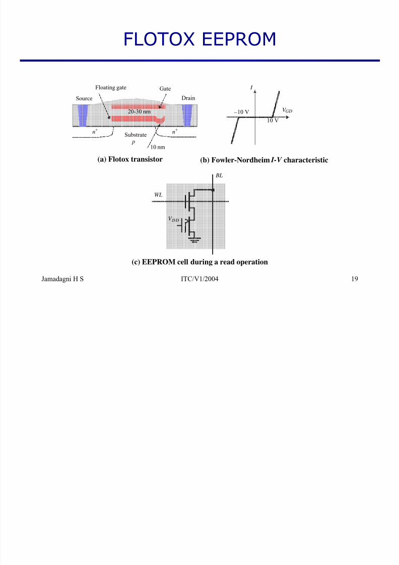
5/17/2018 Learning Material - VLSI Design - slidepdf.com
http://slidepdf.com/reader/full/learning-material-vlsi-design 102/172
Jamadagni H S ITC/V1/2004 19
Source Drain
GateFloating gate
Substraten+n+
10 nm
20-30 nm
(a) Flotox transistor
V GD
I
(b) Fowler-Nordheim I-V characteristic
10 V
−10 V
p
BL
WL
V DD
(c) EEPROM cell during a read operation
Flash EEPROM

5/17/2018 Learning Material - VLSI Design - slidepdf.com
http://slidepdf.com/reader/full/learning-material-vlsi-design 103/172
Jamadagni H S ITC/V1/2004 20
n+ drainn+ source
p-substrate
Control gate
Floating gate
programming
erasure Thin tunneling oxide
Characteristics of State-of-the-art NVM

5/17/2018 Learning Material - VLSI Design - slidepdf.com
http://slidepdf.com/reader/full/learning-material-vlsi-design 104/172
Jamadagni H S ITC/V1/2004 21
Read-Write Memories (RAM)

5/17/2018 Learning Material - VLSI Design - slidepdf.com
http://slidepdf.com/reader/full/learning-material-vlsi-design 105/172
Jamadagni H S ITC/V1/2004 22
• STATIC (SRAM)
• DYNAMIC (DRAM)
Data stored as long as supply is applied
Large (6 transistors/cell)
Fast
Differential
Periodic refresh required
Small (1-3 transistors/cell)
Slower
Single Ended
6-transistor CMOS SRAM Cell

5/17/2018 Learning Material - VLSI Design - slidepdf.com
http://slidepdf.com/reader/full/learning-material-vlsi-design 106/172
Jamadagni H S ITC/V1/2004 23
V DD
Q
Q
M 1 M 3
M 4 M 2
M 5
BL
WL
BL
M 6
CMOS SRAM Analysis (Write)

5/17/2018 Learning Material - VLSI Design - slidepdf.com
http://slidepdf.com/reader/full/learning-material-vlsi-design 107/172
Jamadagni H S ITC/V1/2004 24
V DD
Q = 1Q = 0
M 1
M 4
M 5
BL = 1
WL
BL = 0
M 6
V DD
n M6, VDD VTn–( )VDD
2-----------V
DD
2
8-----------–⎝ ⎠⎛ ⎞ k p M4, VDD VTp–( )
VDD
2-----------V
DD
2
8-----------–⎝ ⎠⎛ ⎞=
n M5,2
------------VDD
2----------- VTn
VDD
2-----------⎝ ⎠⎛ ⎞–
⎝ ⎠⎛ ⎞
2
k n M1, VDD VTn–( )VDD
2-----------
VDD2
8-----------–
⎝ ⎠⎛ ⎞= (W / L)n,M 5 ≥ 10 (W / L)n,M 1
(W / L)n,M 6 ≥ 0.33 (W / L) p,M 4
CMOS SRAM Analysis (Read)

5/17/2018 Learning Material - VLSI Design - slidepdf.com
http://slidepdf.com/reader/full/learning-material-vlsi-design 108/172
Jamadagni H S ITC/V1/2004 25
V DD
Q = 1
Q = 0
M 1
M 4
M 5
BL
WL
BL
M 6
V DDV DDV DD
C bit C bit
k n M5,2
---------------VDD
2------------ VTn
VDD
2------------⎝ ⎠⎛ ⎞–⎝ ⎠
⎛ ⎞2
k n M1, VDD VTn–( )VDD
2------------
VDD2
8------------–⎝ ⎠
⎛ ⎞=
(W / L)n,M 5 ≤ 10 (W / L)n,M 1 (supercedes read constraint)
6T-SRAM — Layout

5/17/2018 Learning Material - VLSI Design - slidepdf.com
http://slidepdf.com/reader/full/learning-material-vlsi-design 109/172
Jamadagni H S ITC/V1/2004 26
VDD
GND
WL
BLBL
M1 M3
M4M2
M5 M6
Resistance-load SRAM Cell
WL

5/17/2018 Learning Material - VLSI Design - slidepdf.com
http://slidepdf.com/reader/full/learning-material-vlsi-design 110/172
Jamadagni H S ITC/V1/2004 27
V DD
M 1 M 2
M 3
BL
WL
BL
M 4
R L R L
Static power dissipation -- Want RL largeBit lines precharged to VDD to address tp problem
3-Transistor DRAM Cell

5/17/2018 Learning Material - VLSI Design - slidepdf.com
http://slidepdf.com/reader/full/learning-material-vlsi-design 111/172
Jamadagni H S ITC/V1/2004 28
M 2
M 1
BL1
WWL
BL2
M 3
RWL
C S
X
WWL
RWL
X
BL1
BL2
V DD-V T
∆V
V DD
V DD-V T
No constraints on device ratiosReads are non-destructiveValue stored at node X when writing a “1” = VWWL-VTn
3T-DRAM — Layout

5/17/2018 Learning Material - VLSI Design - slidepdf.com
http://slidepdf.com/reader/full/learning-material-vlsi-design 112/172
Jamadagni H S ITC/V1/2004 29
BL2 BL1 GND
RWL
WWL
M3
M2
M1
1-Transistor DRAM Cell

5/17/2018 Learning Material - VLSI Design - slidepdf.com
http://slidepdf.com/reader/full/learning-material-vlsi-design 113/172
Jamadagni H S ITC/V1/2004 30
C S M 1
BL
WL
C BL
WL
X
BL
V DD−V T
V DD /2
V DD
GND
Write "1" Read "1"
sensingV DD
/2
∆V VBL VPRE– VBIT VPRE–( )CS
CS CBL+------------------------= =
Write: CS is charged or discharged by asserting WL and BL.Read: Charge redistribution takes places between bit line and storage capacitance
Voltage swing is small; typically around 250 mV.
DRAM Cell Observations

5/17/2018 Learning Material - VLSI Design - slidepdf.com
http://slidepdf.com/reader/full/learning-material-vlsi-design 114/172
Jamadagni H S ITC/V1/2004 31
1T DRAM requires a sense amplifier for each bit line, due to
charge redistribution read-out.
DRAM memory cells are single ended in contrast to SRAM cells.
The read-out of the 1T DRAM cell is destructive; read and
refresh operations are necessary for correct operation.
Unlike 3T cell, 1T cell requires presence of an extra capacitance
that must be explicitly included in the design.
When writing a “1” into a DRAM cell, a threshold voltage is lost.
This charge loss can be circumvented by bootstrapping theword lines to a higher value than VDD.
1-T DRAM Cell
Capacitor

5/17/2018 Learning Material - VLSI Design - slidepdf.com
http://slidepdf.com/reader/full/learning-material-vlsi-design 115/172
Jamadagni H S ITC/V1/2004 32
(a) Cross-section
(b) Layout
Diffused
bit line
Polysilicon
plate
M1 word
line
Capacitor
Polysilicon
gate
Metal word line
SiO2
n+Field Oxide
Inversion layer
induced byplate bias
n+
poly
poly
Used Polysilicon-Diffusion Capacitance
Expensive in Area
Periphery

5/17/2018 Learning Material - VLSI Design - slidepdf.com
http://slidepdf.com/reader/full/learning-material-vlsi-design 116/172
Jamadagni H S ITC/V1/2004 33
• Decoders
• Sense Amplifiers
• Input/Output Buffers
• Control / Timing Circuitry
Row Decoders

5/17/2018 Learning Material - VLSI Design - slidepdf.com
http://slidepdf.com/reader/full/learning-material-vlsi-design 117/172
Jamadagni H S ITC/V1/2004 34
Col lec t ion o f 2 M com p lex log ic ga t es
Org an ized in regu la r and dense fash ion
( N) AND Decoder
NOR Decod er
Dynamic Decoders
GND GNDPrecharge devices

5/17/2018 Learning Material - VLSI Design - slidepdf.com
http://slidepdf.com/reader/full/learning-material-vlsi-design 118/172
Jamadagni H S ITC/V1/2004 35
WL3
GND GNDPrecharge devices
WL2
WL1
WL0
V DD φ A0 A0 A1 A1 A0 A0 A1 A1
V DD
V DD
V DD
V DD
φ
WL3
WL2
WL1
WL0
Dynamic 2-to-4 NOR decoder 2-to-4 MOS dynamic NAND Decoder
Propagation delay is primary concern
A NAND decoder using 2-input pre-decoders

5/17/2018 Learning Material - VLSI Design - slidepdf.com
http://slidepdf.com/reader/full/learning-material-vlsi-design 119/172
Jamadagni H S ITC/V1/2004 36
A0A1 A0A1 A0A1 A0A1 A2A3 A2A3 A2A3 A2A3
A1 A0 A0 A1 A3 A2 A2 A3
WL0
WL1
Splitting decoder into two or more logic layersproduces a faster and cheaper implementation
4 input pass-transistor based column decoder

5/17/2018 Learning Material - VLSI Design - slidepdf.com
http://slidepdf.com/reader/full/learning-material-vlsi-design 120/172
Jamadagni H S ITC/V1/2004 37
BL0 BL1 BL2 BL3
D
A0
A1
S0
S1
S2
S3 2 i n p
u t N O R
d e c o d e r
vantage: speed (tpd does not add to overall memory access time)
advantage: large transistor count
only 1 extra transistor in signal path
4-to-1 tree based column decoder
BL0 BL1 BL2 BL3

5/17/2018 Learning Material - VLSI Design - slidepdf.com
http://slidepdf.com/reader/full/learning-material-vlsi-design 121/172
Jamadagni H S ITC/V1/2004 38
BL0 BL1 BL2 BL3
D
A0
A0
A1
A1
Number of devices drastically reduced
Delay increases quadratically with # of sections; prohibitive for large decodersbuffers
progressive sizing
combination of tree and pass transistor approaches
Solutions:
Decoder for circular shift-register

5/17/2018 Learning Material - VLSI Design - slidepdf.com
http://slidepdf.com/reader/full/learning-material-vlsi-design 122/172
Jamadagni H S ITC/V1/2004 39
φ
φ φ
φ
VDDVDD
φ
φ φ
φ
VDDVDD
φ
φ φ
φ
VDDVDD
RRR
VDD
...
WL0 WL1 WL2
Sense Amplifiers
make ∆V as small

5/17/2018 Learning Material - VLSI Design - slidepdf.com
http://slidepdf.com/reader/full/learning-material-vlsi-design 123/172
Jamadagni H S ITC/V1/2004 40
tp
C ∆V⋅Iav
----------------=
make ∆V as small
as possible
smalllarge
Idea: Use Sense Amplifer
outputinput
s.a.smalltransition
Differential Sensing - SRAM
VDD VDD

5/17/2018 Learning Material - VLSI Design - slidepdf.com
http://slidepdf.com/reader/full/learning-material-vlsi-design 124/172
Jamadagni H S ITC/V1/2004 41
Diff.SenseAmp
BLBL
SRAM cell i
x x
y yD D
VDDVDD
WLi
PC
EQ
DD
x x
y
SE
DD
xx
y
SE
VDD
x x
y
SE
(b) Doubled-ended Current Mirror Amplifier
y
(a) SRAM sensing scheme.(c) Cross-Coupled Amplifier
M1 M2
M4M3
M5
Latch-Based Sense Amplifier
EQ

5/17/2018 Learning Material - VLSI Design - slidepdf.com
http://slidepdf.com/reader/full/learning-material-vlsi-design 125/172
Jamadagni H S ITC/V1/2004 42
VDD
BL
SE
SE
BL
EQ
Initialized in its meta-stable point with EQOnce adequate voltage gap created, sense amp enabled with SEPositive feedback quickly forces output to a stable operating point.
Single-to-Differential Conversion

5/17/2018 Learning Material - VLSI Design - slidepdf.com
http://slidepdf.com/reader/full/learning-material-vlsi-design 126/172
Jamadagni H S ITC/V1/2004 43
Diff.
S.A.cell
BL
Vref +_
WL
x x
y y
How to make good Vref ?
Open bitline architecture
EQ

5/17/2018 Learning Material - VLSI Design - slidepdf.com
http://slidepdf.com/reader/full/learning-material-vlsi-design 127/172
Jamadagni H S ITC/V1/2004 44
VDD
SE
SE
CS CS CS
L
...CSCS
...CS
R
BLL BLR
L0L1 R0 R1
dummycell
dummycell
Q
DRAM Read Process with Dummy Cell
6 0

5/17/2018 Learning Material - VLSI Design - slidepdf.com
http://slidepdf.com/reader/full/learning-material-vlsi-design 128/172
Jamadagni H S ITC/V1/2004 45
0 1 2 3 4 5t (nsec)
0.0
2.0
4.0
6.0
V
( V o
l t )
0 1 2 3 4 5t (nsec)
0.0
2.0
4.0
6.0
V
( V o l t )
0 1 2 3 4 50.0
1.02.0
3.0
4.0
5.0
V
( V o l t )
EQ
WL
SE
BL
BL
BL
BL
(a) reading a zero
(b) reading a one
(c) control signals
Single-Ended Cascode Amplifier
VDD

5/17/2018 Learning Material - VLSI Design - slidepdf.com
http://slidepdf.com/reader/full/learning-material-vlsi-design 129/172
Jamadagni H S ITC/V1/2004 46
WL
WLC
V casc
DRAM Timing

5/17/2018 Learning Material - VLSI Design - slidepdf.com
http://slidepdf.com/reader/full/learning-material-vlsi-design 130/172
Jamadagni H S ITC/V1/2004 47
Address Transition Detection
VDD

5/17/2018 Learning Material - VLSI Design - slidepdf.com
http://slidepdf.com/reader/full/learning-material-vlsi-design 131/172
Jamadagni H S ITC/V1/2004 48
DELAYtdA0
DELAY
td
DELAY
td
ATD
...
A1
AN-1
ATD
Reliability and Yield

5/17/2018 Learning Material - VLSI Design - slidepdf.com
http://slidepdf.com/reader/full/learning-material-vlsi-design 132/172
Jamadagni H S ITC/V1/2004 49
Open Bit-line Architecture —Cross Coupling
EQ

5/17/2018 Learning Material - VLSI Design - slidepdf.com
http://slidepdf.com/reader/full/learning-material-vlsi-design 133/172
Jamadagni H S ITC/V1/2004 50
Sense
AmplifierC C CCCC
WL1 WL0 WLD WLD WL0 WL1
EQ
CWB LCWB L
CBL
BL
CBL
BL
Folded-Bitline Architecture

5/17/2018 Learning Material - VLSI Design - slidepdf.com
http://slidepdf.com/reader/full/learning-material-vlsi-design 134/172
Jamadagni H S ITC/V1/2004 51
BL
...
WLDWLD
BL
y
yx
x
WL0
CCCCCC
EQ
Sense
Amplifier
WL0WL1WL1
CBL
CBL
CWBL
CWB L
Transposed-Bitline Architecture
BL’

5/17/2018 Learning Material - VLSI Design - slidepdf.com
http://slidepdf.com/reader/full/learning-material-vlsi-design 135/172
Jamadagni H S ITC/V1/2004 52
BL
BL
BL’
BL"
SA
Ccross
SABL
BL
BL’
BL"
Ccross
(a) Straightforward bitline routing.
(b) Transposed bitline architecture.
Alpha-particles

5/17/2018 Learning Material - VLSI Design - slidepdf.com
http://slidepdf.com/reader/full/learning-material-vlsi-design 136/172
Jamadagni H S ITC/V1/2004 53
WL
BL
VDD
n+SiO2
α-particle
1 particle ~ 1 million carriers
Yield

5/17/2018 Learning Material - VLSI Design - slidepdf.com
http://slidepdf.com/reader/full/learning-material-vlsi-design 137/172
Jamadagni H S ITC/V1/2004 54
Yield curves at different stages of process maturity(from [Veendrick92])
Redundancy
Row
Add

5/17/2018 Learning Material - VLSI Design - slidepdf.com
http://slidepdf.com/reader/full/learning-material-vlsi-design 138/172
Jamadagni H S ITC/V1/2004 55
Memory
Array
Redundant
columns
Redundant
rows
Column Decoder
R o w D e c o d e r
Address
Column
Address
Fuse
Bank :
Redundancy and Error Correction

5/17/2018 Learning Material - VLSI Design - slidepdf.com
http://slidepdf.com/reader/full/learning-material-vlsi-design 139/172
Jamadagni H S ITC/V1/2004 56
Programmable Logic Array
Product Terms

5/17/2018 Learning Material - VLSI Design - slidepdf.com
http://slidepdf.com/reader/full/learning-material-vlsi-design 140/172
Jamadagni H S ITC/V1/2004 57
x0 x1 x2
f 0 f 1
ANDPLANE
ORPLANE
x0x1
x2
Pseudo-Static PLA
V DDGND GND GND GND

5/17/2018 Learning Material - VLSI Design - slidepdf.com
http://slidepdf.com/reader/full/learning-material-vlsi-design 141/172
Jamadagni H S ITC/V1/2004 58
f 0 f 1
GND
GND
GND
x0 x0 x1 x1 x2 x2
GN GN GN GN
VDD
AND-PLANE OR-PLANE
Dynamic PLA
VGND
φAND
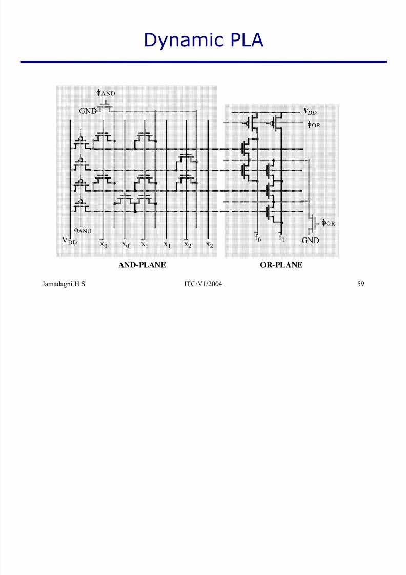
5/17/2018 Learning Material - VLSI Design - slidepdf.com
http://slidepdf.com/reader/full/learning-material-vlsi-design 142/172
Jamadagni H S ITC/V1/2004 59
f 0 f 1 GND
V DD
φOR
x0 x0 x1 x1 x2 x2
GND
VDD
AND-PLANE OR-PLANE
φAND
φOR
Clock Signal Generation for self-timed dynamic PLA
φ φ

5/17/2018 Learning Material - VLSI Design - slidepdf.com
http://slidepdf.com/reader/full/learning-material-vlsi-design 143/172
Jamadagni H S ITC/V1/2004 60
φ
φ AND
φOR
φ φ AND
Dummy AND Row
φ ANDDummy AND Row
φOR
(a) Clock signals (b) Timing generation circuitry.
PLA Layout
VDD GNDφ And-Plane Or-Plane

5/17/2018 Learning Material - VLSI Design - slidepdf.com
http://slidepdf.com/reader/full/learning-material-vlsi-design 144/172
Jamadagni H S ITC/V1/2004 61
f 0 f 1x0 x0 x1 x1 x2 x2
Pull-up devices Pull-up devices
PLA versus ROM
Programmable Logic Arraystructured approach to random logic

5/17/2018 Learning Material - VLSI Design - slidepdf.com
http://slidepdf.com/reader/full/learning-material-vlsi-design 145/172
Jamadagni H S ITC/V1/2004 62
structured approach to random logic
“two level logic implementation”NOR-NOR (product of sums)NAND-NAND (sum of products)
IDENTICAL TO ROM!
Main differenceROM: fully populatedPLA: one element per minterm
Note: Importance of PLA’s has drastically reduced
1. slow2. better software techniques (mutli-level logic
synthesis)
Semiconductor Memory Trends

5/17/2018 Learning Material - VLSI Design - slidepdf.com
http://slidepdf.com/reader/full/learning-material-vlsi-design 146/172
Jamadagni H S ITC/V1/2004 63
Memory Size as a function of time: x 4 every three years
Semiconductor Memory Trends
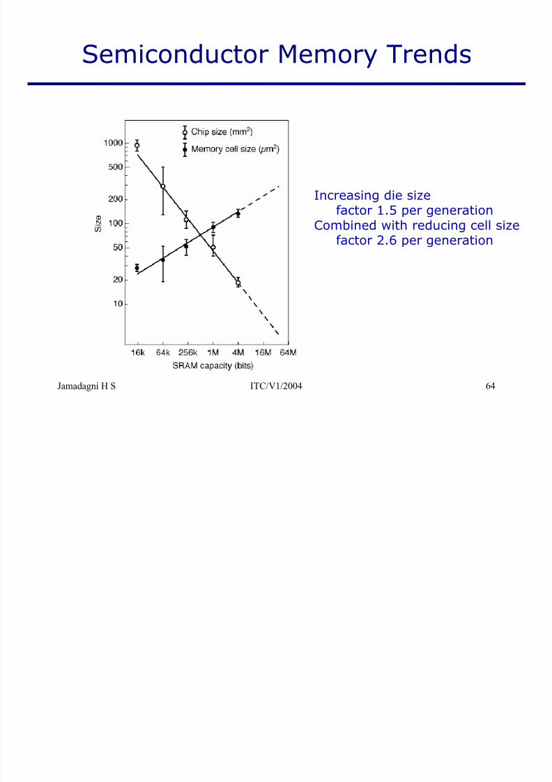
5/17/2018 Learning Material - VLSI Design - slidepdf.com
http://slidepdf.com/reader/full/learning-material-vlsi-design 147/172
Jamadagni H S ITC/V1/2004 64
Increasing die sizefactor 1.5 per generation
Combined with reducing cell sizefactor 2.6 per generation
Semiconductor Memory Trends

5/17/2018 Learning Material - VLSI Design - slidepdf.com
http://slidepdf.com/reader/full/learning-material-vlsi-design 148/172
Jamadagni H S ITC/V1/2004 65
Technology feature size for different SRAM generations
3-Transistor DRAM Cell
BL1
WWL
BL2
WWL

5/17/2018 Learning Material - VLSI Design - slidepdf.com
http://slidepdf.com/reader/full/learning-material-vlsi-design 149/172
Jamadagni HS ITC/V1/2004 1
M 2 M 1
WWL
M 3
RWL
C S
X
RWL
X
BL1
BL2
V DD-V T
∆V
V DD
V DD-V T
No constraints on device ratiosReads are non-destructiveValue stored at node X when writing a “1” = VWWL-VTn
3T-DRAM — Layout
BL2 BL1 GND

5/17/2018 Learning Material - VLSI Design - slidepdf.com
http://slidepdf.com/reader/full/learning-material-vlsi-design 150/172
Jamadagni HS ITC/V1/2004 2
RWL
WWL
M3
M2
M1
1-Transistor DRAM Cell
BL
WL
WL
Write "1" Read "1"

5/17/2018 Learning Material - VLSI Design - slidepdf.com
http://slidepdf.com/reader/full/learning-material-vlsi-design 151/172
Jamadagni HS ITC/V1/2004 3
C S M 1
C BL
X
BL
V DD−V T
V DD /2
V DD
GND
sensing
V DD /2
∆V VBL VPRE– VBIT VPRE–( )CS
CS CBL+------------------------= =
Write: CS is charged or discharged by asserting WL and BL.Read: Charge redistribution takes places between bit line and storage capacitance
Voltage swing is small; typically around 250 mV.
DRAM Cell Observations
1T DRAM requires a sense amplifier for each bit line, due to
charge redistribution read-out.

5/17/2018 Learning Material - VLSI Design - slidepdf.com
http://slidepdf.com/reader/full/learning-material-vlsi-design 152/172
Jamadagni HS ITC/V1/2004 4
g
DRAM memory cells are single ended in contrast to SRAM cells.
The read-out of the 1T DRAM cell is destructive; read and
refresh operations are necessary for correct operation.
Unlike 3T cell, 1T cell requires presence of an extra capacitance
that must be explicitly included in the design.
When writing a “1” into a DRAM cell, a threshold voltage is lost.
This charge loss can be circumvented by bootstrapping theword lines to a higher value than VDD.
1-T DRAM Cell
M1 d
Capacitor
Metal word line

5/17/2018 Learning Material - VLSI Design - slidepdf.com
http://slidepdf.com/reader/full/learning-material-vlsi-design 153/172
Jamadagni HS ITC/V1/2004 5
(a) Cross-section
(b) Layout
Diffused
bit line
Polysilicon
plate
M1 word
line
Polysilicon
gate
SiO2
n+
Field Oxide
Inversion layer
induced by
plate bias
n+
poly
poly
Used Polysilicon-Diffusion Capacitance
Expensive in Area
Periphery
• Decoders

5/17/2018 Learning Material - VLSI Design - slidepdf.com
http://slidepdf.com/reader/full/learning-material-vlsi-design 154/172
Jamadagni HS ITC/V1/2004 6
• Sense Amplifiers
• Input/Output Buffers
• Control / Timing Circuitry
Row Decoders
Collection of 2M complex logic gatesOrganized in regular and dense fashion

5/17/2018 Learning Material - VLSI Design - slidepdf.com
http://slidepdf.com/reader/full/learning-material-vlsi-design 155/172
Jamadagni HS ITC/V1/2004 7
(N)AND Decoder
NOR Decoder
Dynamic Decoders
GND GNDPrecharge devices
V DD
WL3

5/17/2018 Learning Material - VLSI Design - slidepdf.com
http://slidepdf.com/reader/full/learning-material-vlsi-design 156/172
Jamadagni HS ITC/V1/2004 8
WL3
WL2
WL1
WL0
V D D φ A0 A0 A1 A1 A0 A0 A1 A1
V DD
V DD
V DD
φ
WL2
WL1
WL0
Dynamic 2-to-4 NOR decoder 2-to-4 MOS dynamic NAND Decoder
Propagation delay is primary concern
A NAND decoder using 2-input pre-decoders
WL1

5/17/2018 Learning Material - VLSI Design - slidepdf.com
http://slidepdf.com/reader/full/learning-material-vlsi-design 157/172
Jamadagni HS ITC/V1/2004 9
A0A1 A0A1 A0A1 A0A1 A2A3 A2A3 A2A3 A2A3
A1 A0 A0 A1 A3 A2 A2 A3
WL0
Splitting decoder into two or more logic layersproduces a faster and cheaper implementation
4 input pass-transistor based columndecoder
BL0 BL1 BL2 BL3
S

5/17/2018 Learning Material - VLSI Design - slidepdf.com
http://slidepdf.com/reader/full/learning-material-vlsi-design 158/172
Jamadagni HS ITC/V1/2004 10
D
A0
A1
S0
S1
S2
S3 2 i n
p u t N O R
d e c o d e r
vantage: speed (tpd does not add to overall memory access time)
advantage: large transistor count
only 1 extra transistor in signal path
4-to-1 tree based column decoder
BL0 BL1 BL2 BL3
A0

5/17/2018 Learning Material - VLSI Design - slidepdf.com
http://slidepdf.com/reader/full/learning-material-vlsi-design 159/172
Jamadagni HS ITC/V1/2004 11
D
A0
A1
A1
Number of devices drastically reduced
Delay increases quadratically with # of sections; prohibitive for large decoders
buffers
progressive sizing
combination of tree and pass transistor approaches
Solutions:
Decoder for circular shift-register
VDDVDD VDDVDD VDDVDD

5/17/2018 Learning Material - VLSI Design - slidepdf.com
http://slidepdf.com/reader/full/learning-material-vlsi-design 160/172
Jamadagni HS ITC/V1/2004 12
φ
φ φ
φφ
φ φ
φ φ
φ φ
φRRR
VDD
...
WL0 WL1 WL2
Sense Amplifiers
tp
C ∆V⋅
Iav
----------------=
make ∆V as small
as possible

5/17/2018 Learning Material - VLSI Design - slidepdf.com
http://slidepdf.com/reader/full/learning-material-vlsi-design 161/172
Jamadagni HS ITC/V1/2004 13
smalllarge
Idea: Use Sense Amplifer
outputinput
s.a.smalltransition
Differential Sensing - SRAM
VDDVDD PC
VDD
y
VDD
y
M1 M2
M4M3

5/17/2018 Learning Material - VLSI Design - slidepdf.com
http://slidepdf.com/reader/full/learning-material-vlsi-design 162/172
Jamadagni HS ITC/V1/2004 14
Diff.SenseAmp
BLBL
SRAM cell i
x x
y y
D D
WLi
EQx x
SE
xx
SE
VDD
x x
y
SE
(b) Doubled-ended Current Mirror Amplifier
y
(a) SRAM sensing scheme.(c) Cross-Coupled Amplifier
M1 M2
M5
Latch-Based Sense Amplifier
VDD
BL BL
EQ

5/17/2018 Learning Material - VLSI Design - slidepdf.com
http://slidepdf.com/reader/full/learning-material-vlsi-design 163/172
Jamadagni HS ITC/V1/2004 15
DD
SE
SE
Initialized in its meta-stable point with EQOnce adequate voltage gap created, sense amp enabled with SEPositive feedback quickly forces output to a stable operating point.
Single-to-Differential Conversion
BL
WL

5/17/2018 Learning Material - VLSI Design - slidepdf.com
http://slidepdf.com/reader/full/learning-material-vlsi-design 164/172
Jamadagni HS ITC/V1/2004 16
Diff.
S.A.cell Vref
+_
x x
y y
How to make good Vref ?
Open bitline architecture
LR L0L1 R0 R1
EQ

5/17/2018 Learning Material - VLSI Design - slidepdf.com
http://slidepdf.com/reader/full/learning-material-vlsi-design 165/172
Jamadagni HS ITC/V1/2004 17
VDD
SE
SE
CS CS CS
...CSCS
...CS
BLL BLR
dummy
cell
dummy
cell
DRAM Read Process with Dummy Cell
4.0
6.0
o l t )

5/17/2018 Learning Material - VLSI Design - slidepdf.com
http://slidepdf.com/reader/full/learning-material-vlsi-design 166/172
Jamadagni HS ITC/V1/2004 18
0 1 2 3 4 5t (nsec)
0.0
2.0 V ( V
0 1 2 3 4 5t (nsec)
0.0
2.0
4.0
6.0
V
( V o l t )
0 1 2 3 4 50.0
1.0
2.0
3.0
4.0
5.0
V
( V o l t )
EQ
WL
SE
BLBL
BL
BL
(a) reading a zero
(b) reading a one
(c) control signals
Single-Ended Cascode Amplifier
VDD

5/17/2018 Learning Material - VLSI Design - slidepdf.com
http://slidepdf.com/reader/full/learning-material-vlsi-design 167/172
Jamadagni HS ITC/V1/2004 19
WL
WLC
V cas c
DRAM Timing

5/17/2018 Learning Material - VLSI Design - slidepdf.com
http://slidepdf.com/reader/full/learning-material-vlsi-design 168/172
Jamadagni HS ITC/V1/2004 20
Address Transition Detection
DELAY
VDD

5/17/2018 Learning Material - VLSI Design - slidepdf.com
http://slidepdf.com/reader/full/learning-material-vlsi-design 169/172
Jamadagni HS ITC/V1/2004 21
tdA0
DELAY
td
DELAY
td
ATD
...
A1
AN-1
ATD
Open Bit-line Architecture —Cross Coupling
EQ

5/17/2018 Learning Material - VLSI Design - slidepdf.com
http://slidepdf.com/reader/full/learning-material-vlsi-design 170/172
Jamadagni HS ITC/V1/2004 22
Sense
AmplifierC C CCCC
WL1 WL0 WLD WLD WL0 WL1CWB LCWB L
CBL
BL
CBL
BL
Folded-Bitline Architecture
WLDWLDWL0WL0WL1WL1
CWBL

5/17/2018 Learning Material - VLSI Design - slidepdf.com
http://slidepdf.com/reader/full/learning-material-vlsi-design 171/172
Jamadagni HS ITC/V1/2004 23
BL
...
BL
y
yx
x
CCCCCC
EQ
Sense
Amplifier
CBL
CBL
WBL
CWB L
Transposed-Bitline Architecture
BL
BL
BL’
SA
Ccross

5/17/2018 Learning Material - VLSI Design - slidepdf.com
http://slidepdf.com/reader/full/learning-material-vlsi-design 172/172
Jamadagni HS ITC/V1/2004 24
BL
BL"
SABL
BL
BL’
BL"
Ccross
(a) Straightforward bitline routing.
(b) Transposed bitline architecture.