Embed Size (px)
Citation preview
An Interactive Learning Environmentfor VLSI Design
JONATHAN ALLEN, FELLOW, IEEE,AND CHRISTOPHER J. TERMAN
Invited Paper
The interactive learning environment (ILE) is designed to com-bine the traditional resources of a textbook with the “hands-on”design experiences that are vital to a real understanding of basicengineering principles. The ILE builds on the technology developedfor the World Wide Web to provide a learning environment that canbe easily accessed from any browser. In addition to browseable text,JAVA-based computer-aided design (CAD) tools can be accessedthrough interactive figures embedded in the text, where students caninvestigate circuit behavior under the guidance of focused tutorials.
Keywords—Computer-aided instruction, design automation, ed-ucational technology, electrical engineering education, integratedcircuit design, interactive computing, unsupervised learning, verylarge scale integration (VLSI).
I. TODAY’S LEARNING ENVIRONMENT
Very large scale integration (VLSI) design classes havebeen very popular at universities for at least two decades andcontinue to be in high demand as students seek to exploit therapidly expanding technological base. Today, these designtechniques are taught by a combination of lectures, recita-tions, teaching assistant tutorial sessions, textbook readingassignments, problem sets, and laboratory exercises, culmi-nating in a term project that is often submitted for fabrica-tion, the resulting chip being returned later for testing. Stu-dents appreciate the increasingly central role of VLSI in ourtechnical culture and seek to understand and appreciate theMOS VLSI design process, even if they do not intend to be-come professional VLSI designers. They sense the excite-ment of creating a design from scratch (i.e., synthesis) and ofactually building something useful. Synthesis implies choiceamong design alternatives and, hence, exploration of the con-sequences of design decisions. However, today’s learning en-
Manuscript received February 2, 1999; revised July 13, 1999.J. Allen is with the MIT Research Laboratory of Electronics, Cambridge,
MA 02139 USA (e-mail: [email protected]).C. J. Terman is with the MIT Laboratory for Computer Science, Cam-
bridge, MA 02139 USA (e-mail: [email protected]).Publisher Item Identifier S 0018-9219(00)00204-8.
vironment does not tightly coordinate the available resourcesto easily and effectively explore a design. Textbooks are usu-ally not designed with a particular computer-aided design(CAD) tool environment in mind, and CAD tools are usu-ally not designed with learning in mind, but instead, the toolsare configured for intensive production use by industrial de-signers. In an educational environment, these tools are oftenhard to load, configure, train for, and use, although they areundoubtedly powerful in the hands of a skilled designer withstrong system maintenance support.
The context of today’s learning environment, however, israpidly changing. Today’s personal computers are powerfuland capable of performing complex algorithms with rapidresponse, even in laptop configurations. Learning environ-ments must also accommodate an expanding audience. Inaddition to the traditional institutional setting that catersto undergraduates and graduate students at the beginningof their careers, there is also increased interest in distancelearning and life-long learning. So there is a diverse setof learners with varying backgrounds and educationalresources at their disposal, thus generating an increasingdemand for learning environments that are suitable forself-study. A broad palette of resources needs to be pro-vided for the individual student, so that each can adaptthese resources to his or her personal learning style. Thatis, there is increasing need for a coordinated set of learningresources from which a solid understanding can be built. Itis probably not possible to devise a single “best” learningenvironment for all students, but it is possible to createa tightly coupled set of interactive learning componentsthat can serve today’s diverse student requirements in aneffective way. With this perspective in mind, we turn firstto an elaboration of our goals, then a characterization ofan “ideal” learning environment, and finally a descriptionof our functional implementation of an interactive learningenvironment (ILE) that seeks to approximate these ideals.
Our goal is to help students learn goal-oriented design ofMOS digital circuits using realistic technologies.
0018–9219/00$10.00 © 2000 IEEE
96 PROCEEDINGS OF THE IEEE, VOL. 88, NO. 1, JANUARY 2000
• Our emphasis is on learning rather than teaching. Webelieve in learning by doing. The student can best learnto create these circuits by actually designing them per-sonally, as well as exploring all aspects of existing de-signs.
• Our emphasis is on design, or synthesis, although werealize that, to create the best designs, it is essentialto analyze new and existing designs comprehensively.There is an interactive tension between analysis andsynthesis, which is required, in part, due to the lack ofperfect modularity; e.g., the interaction between con-nected modules that may require adjustment for bothcorrectness and performance.
• We emphasize goal-oriented design, where tradeoffsare examined over a set of designs that range overvarying speed, size, and power dissipation.
• We emphasize the centrality of the circuit representa-tion as key to design. The circuit is the highest level ofIC design abstraction that still directly represents thosephysical parameters responsible for performance. (Thenext level higher is the logic level.) Although we alsofocus on layout as the necessary specification to in-terface with fabrication processes, we always extractthe circuit representation from layout in order to assessboth logical correctness and circuit performance.
• We are concerned with a design environment for dig-ital MOS circuits. These are large-swing nonlinear cir-cuits, where the focus is on the digital logic abstrac-tion relation to the circuit, including voltage levels andtransitions, and where the possibility of noise pertur-bations (through both resistive and capacitive coupling)must be considered. As such, although circuit equationscan be written for these circuits, they cannot be solvedin closed form. So, detailed circuit understanding re-quires simulation to accurately derive the relevant volt-ages and currents.
• Our design environment utilizes realistic devicemodels, including parasitics, so that meaningful quan-titative simulation results can be computed. Accuratemodels for interconnect are also derived from thetechnology.
II. THE IDEAL LEARNING ENVIRONMENT
In order to realize our goals, we first conceptualize the na-ture of a design environment that would be ideally suited forproviding the sorts of learning experiences we have in mind.There are several components of this ideal environment thatwe think should be tightly integrated in a single environment(see Fig. 1).
A. Texts
Traditionally, many students have learned IC design froma text. Good design texts provide background, motivation,organization of a substantial volume of material, and explo-ration of many facets of IC design at varying levels of detail.
Fig. 1. ILE block diagram.
They provide the theory to support the intuition and expe-rience that comes from exploring many designs. Texts areinherently linear, hence they are not well suited to showingmultiple simultaneous relationships, although they are wellsuited to providing a taxonomy of material. Texts have theirown hierarchy and modularity, and they are usually orga-nized by the type of circuit or style (e.g., generalized in-verters driving a capacitive load), so that a comprehensivecircuit repertoire is exhibited. Good texts highlight generalprinciples, provide insightful explanations of circuit actionand features, and reveal intercircuit relationships. They areless well suited for the exploration of quantitative circuit de-tail and how circuit parameters and topology interact to pro-vide the resultant performance. Thus, while texts have bothadvantages and disadvantages, they are a useful componentin an overall ideal learning environment.
B. Toolkit
In order to explore each circuit or layout (the two repre-sentations that are central to IC design), an ideal learning en-vironment must include an interactive toolkit of programs.Our vision for the appropriate tools has been inspired by[1]–[4]. The toolkit includes the capability to capture and editschematic and layout representations, to extract circuits fromschematics and layouts, and to simulate circuits. The toolkitalso includes electrical and layout well-formedness checking(e.g., design rule checking), and it can perform equivalence
ALLEN AND TERMAN: INTERACTIVE LEARNING ENVIRONMENT 97
checking between schematic and layout representations. Hi-erarchy, as used in both schematics and layout, is manipu-lated consistently by all programs of the toolkit. By usingthe tools, existing schematics and layouts can be modified(in any respect) and new designs can be created. Thus cir-cuit variations can be studied and comparisons made. Alldesigns, including those provided by the environment andthose created by the user, are savable in a group of libraries(see below). We think it is important to make a direct, seam-less transition from the circuit schematics and layouts in thetext to what the student experiences in the toolkit environ-ment. This can be easily accomplished if one uses the toolkitto present the figures that appear in the text; this has theadded benefit that the figures can be interactive. Usually, thetoolkit focuses on intracircuit properties and relationships,rather than the greater emphasis on intercircuit relationshipsrevealed in the text component.
Once a desired circuit has been created (either from aninitial circuit schematic or extracted from a layout) then itstemporal performance needs to be simulated and displayedin a way that makes it easy to browse and measure. Ideally, itshould be possible to display any current or voltage of the cir-cuit, as well as to display any subset of them simultaneously,by inserting appropriate voltage probes and current metersin the schematic editor. From the display, it must be pos-sible to check on circuit constraints, such as logic levels andpullup/pulldown ratios. It is also highly useful to derive syn-thetic measurements such as device drive , whichhelp to give an idea of the device’s contribution to circuit per-formance. In this way, the learning environment toolkit pro-vides a more extensive understanding of the circuit than thatprovided by the simulator alone. The probes provide a selec-tive level of circuit performance detail and allow the learnerto examine the circuit behavior in any desired way. The probewaveforms are also essential in order to train an intuition forcircuit dynamics, e.g., for charging and discharging of capac-itive nodes.
The ideal design environment must provide for the cre-ation of circuit hierarchy, so that modules can be used repet-itively in an overall design, and so that complex circuits canbe composed for richer functionality from smaller modulesthat can be characterized on their own. Of course, the priceof modularity and hierarchy is often performance, due to thenature of module interfaces, and the ideal environment willfacilitate study of this effect.
In order to compose circuits hierarchically and to pro-mote reuse, modules are organized into libraries. Studentscan share libraries that contain primitive devices, models,sources, probes, example circuits, and useful buildingblocks, e.g., standard cells and memories. Each module hasone or more aspects drawn from an extensible set (e.g., icon,schematic, layout, netlist, and waveform). Per-module prop-erty/value pairs permit the construction of parameterized orgenerated modules.
C. Tutorials
We have seen above that every circuit and layout of theideal text can be instantly edited and simulated, and its wave-
forms displayed. This provides an extraordinarily cohesiveenvironment for learning, but there is so much that can bestudied in even the simplest circuit that guidance in the formof focused tutorials is necessary to steer the student, step bystep, to those aspects of the circuit that are especially im-portant for interactive exploration. For this reason, the ideallearning environment should provide minitutorials that pointout aspects of circuit behavior and suggest ways to modify orexplore it further. In this way, the student is always directedto the study of important effects but still has the capability tostudy any aspect of the circuit.
D. Ease of Access
The ideal learning environment should be available any-where and anytime. It must also allow for easy sharing ofdesigns. It must not present any installation and configura-tion hurdles to the user, so that his or her focus and energy iscentered on the design techniques to be learned, rather thancomplex system overhead.
III. T HE ILE
Given our goals and our sense of an ideal learning envi-ronment for VLSI design, we now turn to a characterizationof our implementation of the ILE for VLSI design.
The ILE is an intimate fusion, or tight coupling, of severalcomponents:
• text, illustrations, toolkit, libraries, focused tutorials,video segments showing talking heads, animation, andother material (and possibly others, as the technologyallows);
• the toolkit (which we call JADE: JAVA Design En-vironment) provides for the design of schematic andlayout representations, their extraction to circuits, sim-ulation (including comparison), and measurement.
Usually these components are loosely juxtaposed in diverseenvironments and media, e.g., paper print, CAD systems, andimage media including stills and video. Traditional ways ofpackaging the components (books, computer software, andvideo tapes) can be cumbersome and not very portable. Inthe ILE, all components are represented digitally in a unifiedenvironment, and any component is easily accessed at anytime. We first discuss the individual components and thenhow they may be used in the ILE.
The text component of the ILE implementation is based onour approach to teaching a semester-length course in VLSIdesign at the Massachusetts Institute of Technology (MIT).The course presumes some background in basic logic for dig-ital design, as well as the device physics of PN junctionsand the MOS capacitor, but these topics are covered at anintroductory level in the text. Students who want more back-ground in these areas can consult the references and otherlinks provided in the text.
The text is meant to provide motivation for schematic de-signs, rigorous explanations of their general modes of be-havior (without numeric values for node voltages and loopcurrents), and a development of general principles for broadclasses of MOS digital circuits and systems. It provides the
98 PROCEEDINGS OF THE IEEE, VOL. 88, NO. 1, JANUARY 2000
overall structure of the course and is the backbone compo-nent of the ILE since it offers a rich multimedia structuredexposition of the entire subject.
There are three major sections of the textual ILE compo-nent. After a brief description of the MOSFET, its principlesof operation, and its current–voltage relationships, the textbuilds a complete schematic repertoire for combinationaland sequential schematics. Once this array of schematicstyles (i.e., families) is provided, the text presents tech-nology mapping of circuits, in order to mask specificationsvia process fabrication families, and the correspondinglayout. Finally, the text considers performance issues (e.g.,high-speed drivers) and special circuits, such as I/O pads.
As we have noted, much of the text develops a compre-hensive repertoire of both combinational and sequentialschematics. After motivating each of these schematics, thetext argues for the topological structure of the schematic, interms of its ability to deliver appropriate digital outputs forselected inputs. The reader should think of these schematics,which are presented in JADE windows through much of thetext, as presentations of abstract circuit families, since theymust be complemented by parameters for all devices, inputsource, and output load circuit fragments, a specification ofthe technology to be used, and the desired JADE analysis,before they can be submitted to JADE for simulation. Thatis, the text-based schematics contain the kernel idea of acomputational module, and the accompanying text general-izes over all circuits with the same schematic kernel. Thetext seeks to provide a basic understanding of this schematicas representing a family, or class, of circuits, all of whichshare the same basic functional properties. The text is, thus,a good place to study a family’s basic properties, usuallywithout regard to detailed numerical performance issues.
The idea of family is further utilized in the text componentof the ILE. Thus the text introduces general discussions ofNMOS and CMOS technologies as families of technologies,whose members share many common features. However, onemember from a technology family must be specified to JADEbefore simulation is possible. The modularity that is providedby recognizing these families with common properties is ofgreat value in understanding the basic ideas in MOS circuitsand in readily switching between members of the family. Forexample, it is simple to switch process specifications withina technology family in order to investigate changes in perfor-mance due to modifications in technology.
Abstract families for source input circuits and output loadcircuits are also provided. Thus, these can readily provide li-braries with useful circuit fragments that can be easily used,along with an element of the schematic family of the kernel,to compose a complete circuit with appropriate parameteri-zation suitable for JADE analysis.
Families, or abstract classes, thus provide the text withthe means to discuss general behavior in an insightful butnonnumeric way. This is a great help when appreciating theschematic function before one is ready to explore detailedcircuit behavior using JADE. The reader can focus on the im-portant ideas presented in the kernel schematic before com-posing a complete circuit for JADE analysis. Once the key
ideas of the schematic family are assimilated, in order to en-able further numerical analysis: the input and output circuitsmust be added to yield a topologically complete schematic;all devices must be parameterized; a technology must bepicked from the technology families; and a desired simu-lation task must be specified (e.g., transient analysis). Allof these are composed in a single JADE window, which isready for the initiation of analysis. Note how the family ab-stract concept preserves the modular aspects of circuit de-sign, and it provides the proper role for the text componentto deal with the generalities common to all members of afamily. This view defines the role of text within the ILE andleaves the detailed numeric study of circuit performance tothe JADE environment, which is equipped to accept the ele-ments of families as inputs needed to study specific circuits.Many of these complete circuits are provided in sample li-braries, along with minitutorials, in order to guide the readerin discovering interesting circuit performance.
The text has been implemented in hypertext form in orderto provide easy integration with other components of the ILE.Fig. 2 shows how the text is displayed with a hierarchicaltable of contents shown on the left side. This arrangementfacilitates jumping to another section of the text without theneed to go to a special section that shows the table of contentsor index.
Another component of the ILE provides video sequences.These are used to show “talking head” overviews (Fig. 2) ofeach chapter of the text, which are brief introductions to theconcepts introduced in the chapter. Video sequences are alsoused, sometimes within the “talking head” presentations, toanimate device and circuit function. Thus the creation of aninverted channel between source and drain, and how it taperswith increasing drain-to-source voltage, is presented with avoice monologue explaining the process. The use of talkingheads personalizes the presentation of material in the ILE andgives the student some sense of the instructor’s style. The textalso includes pictures of early devices and circuits in order toprovide some sense of historical context. In addition, the textcomponent provides the derivation of circuit equations andan explanation of the regions of operation for MOSFET’s.
It is important to note that the text is organized in abottom-up way. We start with the individual MOS device,then describe inverters, and continue to build the schematicrepertoire until we are ready to describe how they aremapped to layout masks, which in turn are interpreted byfabrication processes to produce the final IC chip. In thisway, the student has a firm understanding of physical circuitaction before higher level abstractions are introduced. Thetext repeatedly emphasizes the need to quickly translatebetween different levels of circuit representation.
We emphasize that schematics and layout, together withtheir mappings to circuits, are special in our learning envi-ronment. For this reason, a key feature of the ILE is howthese two representations are introduced in the text. In a con-ventional text, we would expect to see a drawing of a cir-cuit schematic accompanying the discussion of that circuit.However, in the ILE, the drawing is replaced by an embeddedwindow of the JADE toolkit that shows the schematic of in-
ALLEN AND TERMAN: INTERACTIVE LEARNING ENVIRONMENT 99

Fig. 2. Browsing an ILE document with contents sidebar, video clip, and text.
terest (Fig. 3). This means the student can instantly edit theaugmented schematic, extract its SPICE netlist, and simulateit without leaving the text component. Thus the toolkit andtext are very tightly coupled components of the ILE, and theschematic is already drawn within the text in editable formfor further exploration. In this way, the ability of the studentto discover many aspects of the circuit behavior is stronglyenhanced. In order to guide this exploration, focused tuto-rials associated with each schematic are presented to guidethe student to interesting aspects of the circuit behavior.
Layout is treated in a similar way. When a layout view ispresented in the text, it is not just a static drawing, but anembedded window into the JADE toolkit environment wherethe layout can be edited, extracted to circuit netlist form,and simulated. For either schematics or layout, the associatedsimulated circuit can be augmented with voltage probes andcurrent meters at any node or branch. Precise measurementscan be made, thus facilitating not only basic understandingof the circuit action, but also important aspects of its per-formance. The user of the ILE can sense the schematics andlayouts of the text “coming to life” by means of the toolkitcomponent resources.
The text component presents a series of topics, for eachof which the other components can add a complementarydimension. The user of the ILE can select a tightly cou-pled subset of component resources to associate with any
given text topic. Thus the JADE embedded windows usedas text figures and the “talking heads” used as text chapteroverviews are examples of how the ILE provides closelybound component resources associated with the textual topicthemes. It is important to note that the ILE components havean extent or depth that allows the student to pursue aspects oftopics comprehensively. Thus, for example, the student canexplore a circuit’s behavior by: using the schematic editing,extraction, simulation, and measurement capabilities of theJADE toolkit; following suggestions in the text component;using a focused tutorial; or following one’s own inclination.
Because of the tight coupling, it is possible to selectivelybind in adavnce certain aspects of some components to thetopic of interest. Thus the capture of a specific schematic,the associated textual discussion, and the set of minitutorialsrelevant to the investigation of a circuit that can be boundearly, just as a figure of a circuit schematic is bound to thepart of the text that discusses that circuit in a conventionaltext.
Hierarchy is manipulated consistently by all programs ofthe toolkit, and hence there are correspondence zones be-tween corresponding parts of different representations of thesame fundamental entity (circuit). Note that a fully specifiedcircuit includes its inputs too, and hence (in a dependencesense) all voltage and current waveforms for that particularcircuit configuration.
100 PROCEEDINGS OF THE IEEE, VOL. 88, NO. 1, JANUARY 2000

Fig. 3. ILE text with embedded interactive figure; active tutorial window is open at upper right.
IV. EXAMPLES
We have found that the ability to study circuit behavioreasily, in detail, and with realistic accuracy permits a vastlydeeper understanding of circuits, both for instructors and stu-dents, than can be provided by a conventional text with staticfigures. Even the simplest circuit provides endless opportu-nity to gain new insight into circuit function, thus raisingquestions and furnishing the means to acquire a new perspec-tive on basic circuit function. The toolkit provides a virtuallaboratory that can be used anywhere and anytime.
In this section, we provide a sampling of how we usedthe ILE to study circuits. For each circuit, we raise impor-tant issues (which would be suggested by the focused tuto-rial components) and then explore the circuit to gain under-standing and insight. We summarize what has been learnedthrough such exploration and comment on how the explo-ration process itself was used. The toolkit provides profes-sional-level resources for studying circuits, so the studentcan be confident that the results obtained are accurate, real-istic (in terms of available processes), and extendable to largeproject-sized systems.
A. Two-InputNAND Gate
Students are often exposed to simple explanations of circuitaction, which mask issues of performance, so there is often a
tendency to move on to “more interesting” circuits. Here, wesee that “slowing down” to appreciate circuit behavior fullycan bring rich rewards that will provide a more mature contextfor the investigation of more complicated circuits.
Our first example is a simple four-transistor circuit whereonly one of the transistors can exhibit body effect. Its behavioris often described in VLSI texts in terms of theAND effect ofseries FET’s, and theOR effect of parallel FET’s. The readeris readily convinced that theNAND gate produces the correctstatic output levels and that it can be easily extended to moreinputs with the same principles of operation. Beginning stu-dents who are used to turning devices on and off by control-ling the gate voltage are often surprised by the upper pulldownNFET, since, when its input is high, but the lower input is low,it will be turned off by the rising level of its source terminal,which decreases until it equals the (body-effected) de-vice threshold. TheNAND gate also has interesting effects thatsignificantly impact delay in ways that are contrary to intu-ition and conventional wisdom. The student may not be ableto argue simple cause and effect due to the interplay of manyfactors and the transient nature of effects that manifest them-selves only within certain regions of operation.
Here, we study the effect of input arrival time on circuitdelay, as shown in Figs. 4–6, where we simulate two identicalNAND circuits with their inputs reversed. Hence, for the topgate, the top input transitions first; whereas for the bottom
ALLEN AND TERMAN: INTERACTIVE LEARNING ENVIRONMENT 101
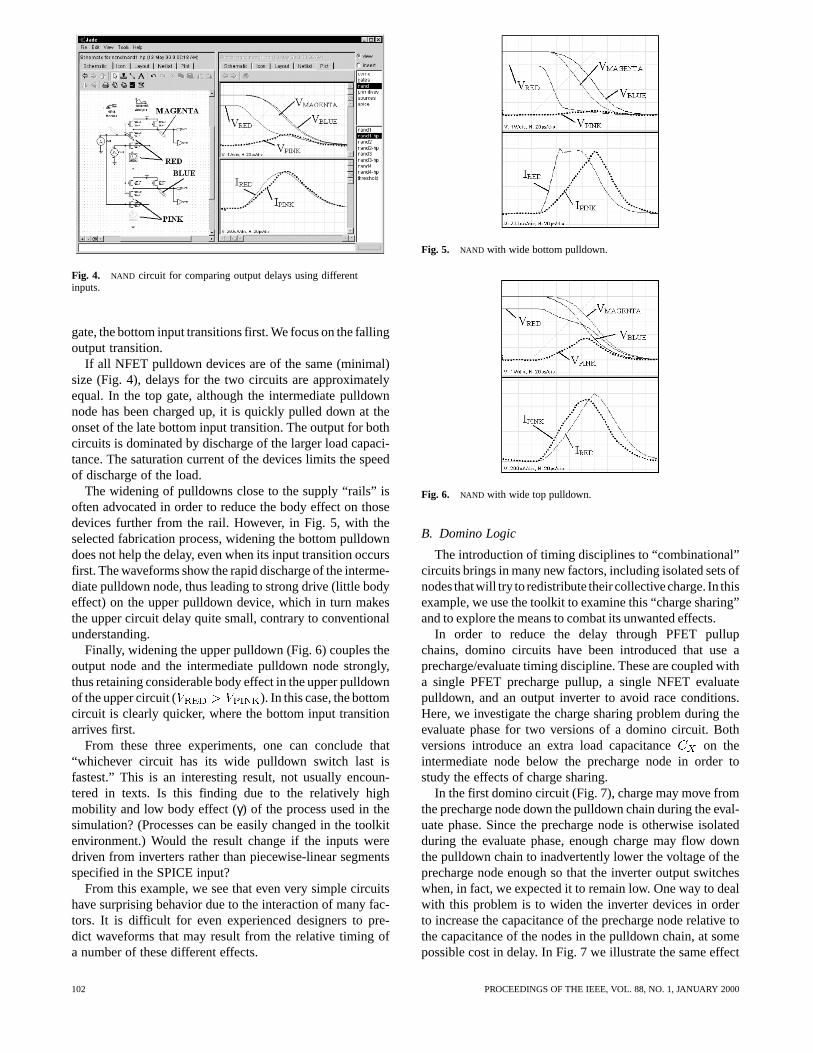
Fig. 4. NAND circuit for comparing output delays using differentinputs.
gate, the bottom input transitions first. We focus on the fallingoutput transition.
If all NFET pulldown devices are of the same (minimal)size (Fig. 4), delays for the two circuits are approximatelyequal. In the top gate, although the intermediate pulldownnode has been charged up, it is quickly pulled down at theonset of the late bottom input transition. The output for bothcircuits is dominated by discharge of the larger load capaci-tance. The saturation current of the devices limits the speedof discharge of the load.
The widening of pulldowns close to the supply “rails” isoften advocated in order to reduce the body effect on thosedevices further from the rail. However, in Fig. 5, with theselected fabrication process, widening the bottom pulldowndoes not help the delay, even when its input transition occursfirst. The waveforms show the rapid discharge of the interme-diate pulldown node, thus leading to strong drive (little bodyeffect) on the upper pulldown device, which in turn makesthe upper circuit delay quite small, contrary to conventionalunderstanding.
Finally, widening the upper pulldown (Fig. 6) couples theoutput node and the intermediate pulldown node strongly,thus retaining considerable body effect in the upper pulldownof the upper circuit ( ). In this case, the bottomcircuit is clearly quicker, where the bottom input transitionarrives first.
From these three experiments, one can conclude that“whichever circuit has its wide pulldown switch last isfastest.” This is an interesting result, not usually encoun-tered in texts. Is this finding due to the relatively highmobility and low body effect (γ) of the process used in thesimulation? (Processes can be easily changed in the toolkitenvironment.) Would the result change if the inputs weredriven from inverters rather than piecewise-linear segmentsspecified in the SPICE input?
From this example, we see that even very simple circuitshave surprising behavior due to the interaction of many fac-tors. It is difficult for even experienced designers to pre-dict waveforms that may result from the relative timing ofa number of these different effects.
Fig. 5. NAND with wide bottom pulldown.
Fig. 6. NAND with wide top pulldown.
B. Domino Logic
The introduction of timing disciplines to “combinational”circuits brings in many new factors, including isolated sets ofnodes thatwill try to redistribute their collectivecharge. In thisexample, we use the toolkit to examine this “charge sharing”and to explore the means to combat its unwanted effects.
In order to reduce the delay through PFET pullupchains, domino circuits have been introduced that use aprecharge/evaluate timing discipline. These are coupled witha single PFET precharge pullup, a single NFET evaluatepulldown, and an output inverter to avoid race conditions.Here, we investigate the charge sharing problem during theevaluate phase for two versions of a domino circuit. Bothversions introduce an extra load capacitance on theintermediate node below the precharge node in order tostudy the effects of charge sharing.
In the first domino circuit (Fig. 7), charge may move fromthe precharge node down the pulldown chain during the eval-uate phase. Since the precharge node is otherwise isolatedduring the evaluate phase, enough charge may flow downthe pulldown chain to inadvertently lower the voltage of theprecharge node enough so that the inverter output switcheswhen, in fact, we expected it to remain low. One way to dealwith this problem is to widen the inverter devices in orderto increase the capacitance of the precharge node relative tothe capacitance of the nodes in the pulldown chain, at somepossible cost in delay. In Fig. 7 we illustrate the same effect
102 PROCEEDINGS OF THE IEEE, VOL. 88, NO. 1, JANUARY 2000

Fig. 7. Charge sharing in a dominoNAND gate.
by manipulating the extra load . Note that when is 7fF (top plot), the inverter output voltage rises a little(less than ), while the precharge node voltagedrops to meet the intermediate node voltage belowit in the pulldown chain. However, when is 10 fF orlarger (bottom plot), the inverter output switches during theevaluate phase, giving rise to a “glitch” that will propagatethrough the domino chain.
In the second domino circuit, we explore another way tocombat the inadvertent switching of the output inverter dueto charge sharing from the precharge node. In this circuit,a feedback PFET “keeper” device is introduced around theoutput inverter, as shown in Fig. 8. When the precharge nodevoltage is high, the inverter output voltage is low, thus holdingthe keeper device on, which bleeds charge from the railinto the precharge node, and replenishing charge that has beenshared down the NFET pulldown chain. (Note that the keeperalso helps to avoid capacitive noise coupling to the prechargenode during the evaluate phase by providing a resistive pathto the rail.) Now, as with the previous domino version,we can increase in order to draw charge off the prechargenode during the evaluate phase. Even whenis increasedto 10 fF (top plot), we see in Fig. 8 that the precharge nodedrops in voltage, but there is only a small glitch (less than
) on the output. has to rise to over 27 fF (bottom plot)before the inverter output voltage switches to a high valuefor the duration of the evaluate phase—which will propagatean error through the domino chain—illustrating the valueof the keeper. By experimenting with the size of the outputinverter devices, the size of the keeper (which must be weakenough to cut off the inverter pulldown when the invertershould correctly switch to a high voltage), the size of theprecharge device, and possible opportunities for minimizingthe capacitance of nodes in the NFET pulldown chain, ahigh-performance domino circuit can be obtained that willnot misbehave due to charge sharing.
C. Sense Amplifier
Most CMOS circuits are designed around the switch-likebehavior of the MOSFET and, after a few weeks of analyzing
Fig. 8. Charge sharing with feedback keeper.
such circuits, students have a good feel for how they work.When confronted with a circuit that exploits a different prop-erty of MOSFET’s (in this case, the relationship between cur-rents and voltages in a saturated device), many students are ata loss to explain how the circuit works, since more is involvedthan the devices simply being “on” or “off.” The purpose ofthis example is not only to teach how sense amps work, butalso to show how to ferret out a reasonable explanation in amethodical fashion.
An interesting design problem is to construct a senseamplifier, which is a circuit used to rapidly detect very smallchanges in the voltage of memory bit lines. While CMOSgates exhibit very high voltage gain at their switchingthreshold, changes in the switching threshold due to varia-tions of temperature, power supply voltages, manufacturingparameters, etc., make it exceedingly difficult to reliablybias the bit line voltage into the high-gain region of thegate input. So, many memories use a variation of thedouble-ended sense amplifier shown in Fig. 9. As shown inthe accompanying waveform plot, a small dip in the voltageof the BIT input quickly results in a large drop in the voltageof the DATA output. Two quick experiments with the circuitshow how it works.
Inserting ammeters into each leg of the pullup and anotherammeter in the common pulldown path (Fig. 10) lets us makesome interesting observations about current flows. Noticethat the current flowing into the bottom NFET is rela-tively constant: that NFET is configured as a current source.Since the total current through the current source is fixed, thecurrent in one leg of the pullup must “mirror” the current inthe other leg, i.e., when the current in one leg drops, the cur-rent in the other leg must increase by the same amount (andvice versa). A small drop in the BIT voltage results in a smalldrop in the current through the right leg of the pullup, whichis then mirrored by a small increase in the current of the otherleg. But why does this lead to such a dramatic change in thevoltage of the DATA output? The key lies in the behaviorof the PFET in the left pullup chain, through which the in-creased current must flow. Let us characterize the behaviorof this PFET using another experiment shown in Fig. 11.
ALLEN AND TERMAN: INTERACTIVE LEARNING ENVIRONMENT 103
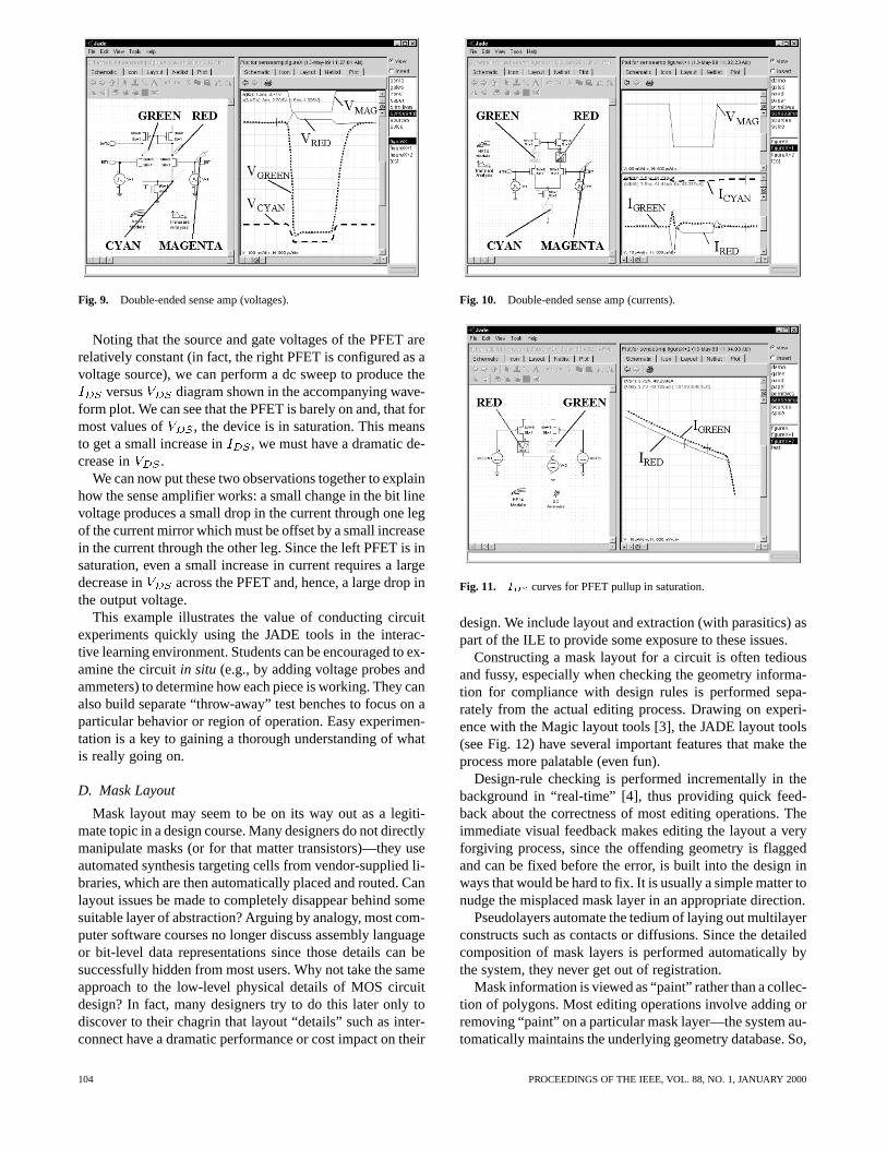
Fig. 9. Double-ended sense amp (voltages).
Noting that the source and gate voltages of the PFET arerelatively constant (in fact, the right PFET is configured as avoltage source), we can perform a dc sweep to produce the
versus diagram shown in the accompanying wave-form plot. We can see that the PFET is barely on and, that formost values of , the device is in saturation. This meansto get a small increase in , we must have a dramatic de-crease in .
We can now put these two observations together to explainhow the sense amplifier works: a small change in the bit linevoltage produces a small drop in the current through one legof the current mirror which must be offset by a small increasein the current through the other leg. Since the left PFET is insaturation, even a small increase in current requires a largedecrease in across the PFET and, hence, a large drop inthe output voltage.
This example illustrates the value of conducting circuitexperiments quickly using the JADE tools in the interac-tive learning environment. Students can be encouraged to ex-amine the circuitin situ (e.g., by adding voltage probes andammeters) to determine how each piece is working. They canalso build separate “throw-away” test benches to focus on aparticular behavior or region of operation. Easy experimen-tation is a key to gaining a thorough understanding of whatis really going on.
D. Mask Layout
Mask layout may seem to be on its way out as a legiti-mate topic in a design course. Many designers do not directlymanipulate masks (or for that matter transistors)—they useautomated synthesis targeting cells from vendor-supplied li-braries, which are then automatically placed and routed. Canlayout issues be made to completely disappear behind somesuitable layer of abstraction? Arguing by analogy, most com-puter software courses no longer discuss assembly languageor bit-level data representations since those details can besuccessfully hidden from most users. Why not take the sameapproach to the low-level physical details of MOS circuitdesign? In fact, many designers try to do this later only todiscover to their chagrin that layout “details” such as inter-connect have a dramatic performance or cost impact on their
Fig. 10. Double-ended sense amp (currents).
Fig. 11. I curves for PFET pullup in saturation.
design. We include layout and extraction (with parasitics) aspart of the ILE to provide some exposure to these issues.
Constructing a mask layout for a circuit is often tediousand fussy, especially when checking the geometry informa-tion for compliance with design rules is performed sepa-rately from the actual editing process. Drawing on experi-ence with the Magic layout tools [3], the JADE layout tools(see Fig. 12) have several important features that make theprocess more palatable (even fun).
Design-rule checking is performed incrementally in thebackground in “real-time” [4], thus providing quick feed-back about the correctness of most editing operations. Theimmediate visual feedback makes editing the layout a veryforgiving process, since the offending geometry is flaggedand can be fixed before the error, is built into the design inways that would be hard to fix. It is usually a simple matter tonudge the misplaced mask layer in an appropriate direction.
Pseudolayers automate the tedium of laying out multilayerconstructs such as contacts or diffusions. Since the detailedcomposition of mask layers is performed automatically bythe system, they never get out of registration.
Mask information is viewed as “paint” rather than a collec-tion of polygons. Most editing operations involve adding orremoving “paint” on a particular mask layer—the system au-tomatically maintains the underlying geometry database. So,
104 PROCEEDINGS OF THE IEEE, VOL. 88, NO. 1, JANUARY 2000
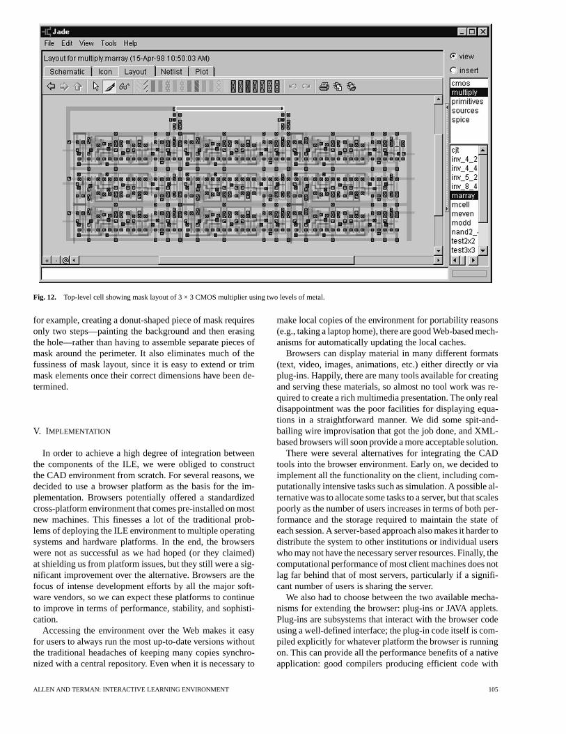
Fig. 12. Top-level cell showing mask layout of 3 × 3 CMOS multiplier using two levels of metal.
for example, creating a donut-shaped piece of mask requiresonly two steps—painting the background and then erasingthe hole—rather than having to assemble separate pieces ofmask around the perimeter. It also eliminates much of thefussiness of mask layout, since it is easy to extend or trimmask elements once their correct dimensions have been de-termined.
V. IMPLEMENTATION
In order to achieve a high degree of integration betweenthe components of the ILE, we were obliged to constructthe CAD environment from scratch. For several reasons, wedecided to use a browser platform as the basis for the im-plementation. Browsers potentially offered a standardizedcross-platform environment that comes pre-installed on mostnew machines. This finesses a lot of the traditional prob-lems of deploying the ILE environment to multiple operatingsystems and hardware platforms. In the end, the browserswere not as successful as we had hoped (or they claimed)at shielding us from platform issues, but they still were a sig-nificant improvement over the alternative. Browsers are thefocus of intense development efforts by all the major soft-ware vendors, so we can expect these platforms to continueto improve in terms of performance, stability, and sophisti-cation.
Accessing the environment over the Web makes it easyfor users to always run the most up-to-date versions withoutthe traditional headaches of keeping many copies synchro-nized with a central repository. Even when it is necessary to
make local copies of the environment for portability reasons(e.g., taking a laptop home), there are good Web-based mech-anisms for automatically updating the local caches.
Browsers can display material in many different formats(text, video, images, animations, etc.) either directly or viaplug-ins. Happily, there are many tools available for creatingand serving these materials, so almost no tool work was re-quired to create a rich multimedia presentation. The only realdisappointment was the poor facilities for displaying equa-tions in a straightforward manner. We did some spit-and-bailing wire improvisation that got the job done, and XML-based browsers will soon provide a more acceptable solution.
There were several alternatives for integrating the CADtools into the browser environment. Early on, we decided toimplement all the functionality on the client, including com-putationally intensive tasks such as simulation. A possible al-ternative was to allocate some tasks to a server, but that scalespoorly as the number of users increases in terms of both per-formance and the storage required to maintain the state ofeach session. A server-based approach also makes it harder todistribute the system to other institutions or individual userswho may not have the necessary server resources. Finally, thecomputational performance of most client machines does notlag far behind that of most servers, particularly if a signifi-cant number of users is sharing the server.
We also had to choose between the two available mecha-nisms for extending the browser: plug-ins or JAVA applets.Plug-ins are subsystems that interact with the browser codeusing a well-defined interface; the plug-in code itself is com-piled explicitly for whatever platform the browser is runningon. This can provide all the performance benefits of a nativeapplication: good compilers producing efficient code with
ALLEN AND TERMAN: INTERACTIVE LEARNING ENVIRONMENT 105
the added advantage of potentially reusing existing tool ker-nels. Unfortunately, plug-ins saddle the developer with all theworries of developing and installing on multiple platforms.We chose to develop the tools in JAVA, which we felt hadseveral advantages. “Write once, run anywhere” is an attrac-tive siren call if one is targeting a diverse community of users.Sadly, this was more illusion than substance—we quicklydiscovered that there were dismaying differences in function-ality and performance among the different JAVA implemen-tations. As a stop-gap measure, we focused on a particularJAVA implementation as the initial target, and it appears thissituation will be remedied in the foreseeable future.
Contrary to expectations, the performance of the toolswritten in JAVA was actually quite good, and it continues toimprove with each new release of the JAVA virtual machine.Coupled with the dizzying improvements in the perfor-mance of the underlying processors, the tools are more thancapable of accommodating reasonable size projects whilemaintaining an acceptable degree of interactivity.
The multithreading support in JAVA made it easy to usebackground multitasking for computationally intensive taskslike simulation and design rule checking. This greatly im-proves the usability of the tools by avoiding the natural ten-sion between accuracy that often requires time-consumingcomputations and responsiveness, which relies on low-la-tency execution of commands.
On-the-fly loading of classes should make it possible toadd new capabilities to the tools (e.g., support for a newmodule aspect such as an HDL representation) without mod-ifications to the existing code.
In order to make the tools as approachable as possible,considerable effort was made to make the user interfaceconsistent with other graphical user interfaces—selection,cut/copy/paste, drag and drop, navigation, choice of buttons,and organization of menus are all as one would expect.Many users can get useful work done after only a fewminutes with the “getting started” tutorial. It is actually funto use the tools, not a feeling one would expect to haveafter experiencing many of the commercially available CADtools.
VI. CONTRIBUTIONS
The ILE seamlessly integrates its components. Upon en-countering a circuit schematic or layout in the text, it is easyto browse and modify the figure using the integrated toolkit.It is easy to pose questions and get answers at any level of de-tail. Thus, students can quickly learn where to look in orderto make low-cost experiments. These experiments build intu-ition about digital MOS circuit behavior and, together withthe appropriate theory supplied in the text component andthe experience gained by repeated experiments, they form asolid background for creating new, innovative MOS circuits.The editor and simulator environment brings “life” to textualdescriptions of circuits, and it facilitates a student’s person-alized understanding of circuits. Because the environmentuses well-known user interface gestures, there is a shallow
learning curve, thus providing the student user with valu-able insight at minimum cost. Being Web-based, the interac-tive learning environment poses zero administrative cost tothe user, thus making it well suited for distance learning andlife-long learning away from an institutional teaching envi-ronment.
VII. FOR MORE INFORMATION
For an online discussion of this special issue, please visitthe discussion website at http://ieee.research.umich.edu.
REFERENCES
[1] S. Rubin,Computer Aids for VLSI Design. Reading, MA: Ad-dison-Wesley, 1987.
[2] J. Cherry, “CAD programming in an object-oriented program-ming environment,” inVLSI CAD Tools and Applications, W.Fichtner and M. Morf, Eds. Norwell, MA: Kluwer AcademicPublishers, 1987, ch. 9.
[3] J. Ousterhout, G. Hamachi, R. Mayo, W. Scott, and G. Taylor,“Magic: A VLSI layout system,” inProc. 21st Design Automa-tion Conf., 1984, pp. 152–159.
[4] G. Taylor and J. Ousterhout, “Magic’s incremental design-rulechecker,” inProc. 21st Design Automation Conf., 1984, pp.160–165.
Jonathan Allen (Fellow IEEE) received theA.B. and M.S. degrees from Dartmouth College,Hanover, NH, and the Ph.D. degree fromMassachusetts Institute of Technology (MIT),Cambridge.
From 1962 to 1968, he worked at Bell Tele-phone Laboratories, where he became the Super-visor of Human Factors Engineering in 1966. In1968, he joined the faculty of the Electrical En-gineering and Computer Science Department atMIT, where he is currently Professor. In 1981, he
was appointed Director of MIT’s Research Laboratory of Electronics. Hisresearch activities at Bell Laboratories involved the design of semi-auto-matic telephone information bureaus and vocoder systems. At MIT, his areasof interest include linguistic techniques for converting unrestricted text tospeech, system design for continuous speech recognition, computer archi-tecture, and custom integrated circuit design.
Dr. Allen is a member of Phi Beta Kappa, Tau Beta Pi, and Sigma Xi. Heis Past President of the Association for Computational Linguistics.
Christopher J. Terman received the B.A.degree in physics from Wesleyan University,Middletown, CT, and the M.S., E.E., and Ph.D.degrees in computer science and engineeringfrom Massachusetts Institute of Technology(MIT), Cambridge.
He is a Senior Lecturer in the MIT Departmentof Electrical Engineering and Computer Scienceand a member of the Laboratory for ComputerScience. As a researcher and faculty member atMIT, he implemented several early prototypes
for microprocessor-based workstations that led to the development of theIEEE–1996 Bus Architecture (the NuBus). In his work on computer-aideddesign (CAD) tools for very large scale integration (VLSI) circuits, hedeveloped algorithms for full-chip transistor-level simulation. During histen years in industry, he cofounded several firms, including Symbolics, Inc.(manufacturer of Lisp Machines), TLW, Inc. (VLSI designs for commu-nications and multimedia), and Curl Corp. (a software technology for theWeb). After returning to MIT, he has worked on developing educationaltechnology for use in teaching design-oriented courses.
106 PROCEEDINGS OF THE IEEE, VOL. 88, NO. 1, JANUARY 2000