Embed Size (px)
Citation preview

Design Guide: TIDA-060029LCR Meter Analog Front-End Reference Design
DescriptionThis reference design, TIDA-060029, demonstratesan analog signal chain solution for LCR Meterapplications using an auto balancing impedancemeasurement method. Auto balancing impedancemeasurement circuits can often be challenging tostabilize because the circuit stability is dependent onboth the value and type of component to bemeasured. Therefore, it is imperative to have a circuitsolution that is inherently stable irrespective of themeasured component's type and value. This designpresents an analog signal-chain solution that is bothinherently stable and accurate to 0.1% for LCR meterapplications.
ResourcesTIDA-60029 Design FolderOPA2810 Product FolderOPA810 Product FolderBUF634A Product Folder
Ask our TI E2E™ support experts
Features• Measures wide range of components (L, C, R) with
impedance values ranging from 1 Ω to 10 MΩ• Frequency of operation up to 100 kHz• Tested at 100 Hz, 1 kHz, 10 kHz, 100 kHz• Impedance accuracy of 0.1 %• Inherently stable operation of the signal chain
Applications• Digital Multimeter (DMM)• Impedance and Vector Network Analyzer• Semiconductor Manufacturing• Semiconductor Test
+
±
OPAx810 BUF634A
R1
R2
R3
ZX
+
±
OPAx810 BUF634A
R1
R2
R3
+
±
OPAx810
+
±
OPAx810
+
±
RFRG
RFRG
+
±
RFRG
RFRG
FDA
FDA ADC
ADC
Not part of TIDA-060029 board
www.ti.com Description
TIDUEU6A – JUNE 2020 – REVISED SEPTEMBER 2020Submit Document Feedback
LCR Meter Analog Front-End Reference Design 1
Copyright © 2020 Texas Instruments Incorporated

1 System DescriptionThe goal of any test and measurement system is to measure a device under test (DUT) as simply as possible,while only introducing errors significantly smaller than those present in the measured device. For impedancemeasurements, there are several existing techniques that provide various tradeoffs between measurementaccuracy, complexity, and frequency range. For this design, the auto balancing circuit method was chosenbecause it provides good accuracy over a wide impedance measurement range without any tuningrequirements. Table 1-1 lists the advantages and disadvantages of several common impedance measurementtechniques along with their frequency ranges and typical applications.
Table 1-1. Impedance Measurement MethodsMETHOD ADVANTAGES DISADVANTAGES APPLICABLE
FREQUENCY RANGECOMMON APPLICATION
Bridge method • High Accuracy• Wide frequency range
with different types ofbridges
• Manual balancingneeded
• Narrow frequencycoverage with singlebridge
DC to 300 MHz Standard Lab
Resonant method • Good Q measurementaccuracy up to high Q
• Tuning required• Low impedance
measurementaccuracy
10 kHz to 70 MHz High Q devicemeasurement
Network analysis method • Wide frequencycoverage
• Good accuracy
• Narrow impedancemeasurement range
5 Hz to above RF componentmeasurement
Auto balancing method(Method used in thisdesign)
• Good accuracy overwide range ofimpedances
• Grounded devicemeasurement
• High frequency rangesare not available
20 Hz to 120 MHz Generic componentmeasurement
The auto balancing technique is very useful for a wide range of impedance measurements at a frequency rangeof 20 Hz to 120 MHz. The auto balancing technique uses an op-amp as shown in Figure 1-1.
+
±ZX
RF
VX
IX
VO = IX * RF
IX
Figure 1-1. Auto Balancing Circuit Amplifier Configuration
The fundamental idea in this technique is to convert the current ( IX ) through unknown impedance (ZX) intovoltage ( VO ). The unknown impedance value is determined using the value of current flowing through it. Thenon-ideal properties of the amplifier and circuit play a very crucial role in the design of an LCR meter. Forexample, the parasitic capacitance at the inverting input of the amplifier will cause instability for a high value ofRF. The circuit's stability is also sensitive to both the type of component and value used for ZX. The circuit isparticularly prone to instability when capacitive impedances are measured. In this design, these stabilityproblems are addressed using a multi-path capacitive compensation technique. This design illustrates theanalog signal chain of an LCR meter which is tested up to 100 kHz.
System Description www.ti.com
2 LCR Meter Analog Front-End Reference Design TIDUEU6A – JUNE 2020 – REVISED SEPTEMBER 2020Submit Document Feedback
Copyright © 2020 Texas Instruments Incorporated

1.1 Key System SpecificationsTable 1-2. Key System Specifications
PARAMETER SPECIFICATIONSResistance Range 1 Ω to 10 MΩ
Capacitance Range 1.76 pF to 1.59 mF
Inductance Range 2.59 µH to 1432 H
Frequencies of Operation 100 Hz, 1 kHz, 10 kHz, 100 kHz
RG – RF Settings 100Ω, 5 kΩ, 100 kΩ
Best % Accuracy 0.1%
Power Supply +/- 12 V
www.ti.com System Description
TIDUEU6A – JUNE 2020 – REVISED SEPTEMBER 2020Submit Document Feedback
LCR Meter Analog Front-End Reference Design 3
Copyright © 2020 Texas Instruments Incorporated

2 System Overview2.1 Block Diagram
+
±
OPAx810 BUF634A
R1
R2
R3
ZX
+
±
OPAx810 BUF634A
R1
R2
R3
+
±
OPAx810
+
±
OPAx810
+
±
RFRG
RFRG
+
±
RFRG
RFRG
FDA
FDA ADC
ADC
Not part of TIDA-060029 board
Figure 2-1. TIDA-060029 Block Diagram
2.2 Highlighted Products2.2.1 OPA2810
The OPA2810 is a dual-channel, FET-input, voltage-feedback operational amplifier with low input bias current of2 pA. The extremely low input bias current is very useful in this application because this current will flow throughunknown impedance which can go high as 10 MΩ. OPA2810 is unity-gain stable with a small-signal unity-gainbandwidth of 105 MHz, and offers excellent DC precision and dynamic AC performance at a low quiescentcurrent. This device has a DC open loop gain equal to 120 dB. With a gain-bandwidth product (GBW) of 70 MHz,the OPA2810 has Aol greater than 60 dB at all the frequencies less 100 kHz. The high Aol of the op ampreduces the error in measurement because as the Aol increases the voltage at the inverting input approaches tozero. Thus, this is very important specification of this device to make it well suited for use in this application. Thesupply voltage of OPA2810 can go up to +/- 13.5 V. This high voltage operation provides optimal distortionperformance in the LCR meter signal chain. The voltage noise of this amplifier is 6 nV/√Hz.
2.2.2 BUF634A
The BUF634A is a high speed wide bandwidth unity gain buffer. It is used in composite loop with the OPA2810 toincrease the output current capability from 100mA to 250 mA. The BUF634A has two bandwidth options of 35MHz and 210 MHz. It is optional to use in this application.
2.3 Design Considerations2.3.1 Existing architecture
The fundamental concept of this design is the conversion of current through ZX into a voltage using anamplification factor of RF. The output of amplifier A2 is given in Equation 1
81 = lF4(<:
p Û 8+0
(1)
If RF is known then Zx can be estimated using Equation 1. Figure 2-2 illustrates this architecture.
System Overview www.ti.com
4 LCR Meter Analog Front-End Reference Design TIDUEU6A – JUNE 2020 – REVISED SEPTEMBER 2020Submit Document Feedback
Copyright © 2020 Texas Instruments Incorporated

A1
+
±
VIN
ZX
A2
+
±
RF
VOUT
VX
Figure 2-2. Basic Impedance Measurement Circuit
In this method, multiple values of RF can be used for multiple ranges of impedance, as shown in Figure 2-6. Thisapproach of using multiple RF values improves the accuracy.
2.3.1.1 Circuit Stability Issue
When the unknown impedance is capacitive as shown in Figure 2-3, the feedback transfer function can becalculated using Equation 2.
1
Ú=81
8(= 1 + 4( Û %: Û 5
(2)
A2
+
±
RF
CX
Figure 2-3. Capacitor Measurement Circuit
The transfer function implies that a zero is formed in 1/β. The frequency of this zero can be calculated usingEquation 3.
ñ< =1
4(Û%:
(3)
It can be seen that the zero frequency depends on the unknown capacitance, CX. In Figure 2-4 it can be seenthat Aolβ has a rate of closure of 40dB/dec. When the zero frequency is more than a decade below fCL, thephase margin will reduce to zero making the circuit unstable.
www.ti.com System Overview
TIDUEU6A – JUNE 2020 – REVISED SEPTEMBER 2020Submit Document Feedback
LCR Meter Analog Front-End Reference Design 5
Copyright © 2020 Texas Instruments Incorporated

Figure 2-4. Bode Plot of Capacitor Measurement
2.3.1.2 Solution in Existing Architecture (Compensation Cap)
The circuit instability issue is resolved in the existing architecture with the help of compensation capacitor CF inparallel with RF as shown in Figure 2-5. The required value of CF also varies with unknown capacitance CX.Hence, it becomes impossible to find single value of CF which can stabilize the circuit for complete range of ZX.
A2
+
±
RF
CX
CF
Figure 2-5. Capacitor Measurement Circuit w/ Compensation Capacitor
System Overview www.ti.com
6 LCR Meter Analog Front-End Reference Design TIDUEU6A – JUNE 2020 – REVISED SEPTEMBER 2020Submit Document Feedback
Copyright © 2020 Texas Instruments Incorporated

2.3.2 Proposed Design
+
±
A1
OPAx810
R1
R2
R3
ZX
+
±
A2
OPAx810
R1
R2
R3
VX
VOUT
Figure 2-6. Impedance Measurement Design
In this method, three different combinations of RG – RF (labeled as R1, R2 & R3 in Figure 2-6) are selected forthree ranges of impedance ZX. The ranges can be seen in Table 2-1. The architecture in this method is verysimilar to the existing architecture explained in last section. The only difference is that the RG is added in serieswith ZX. Also the value of RG is equal to RF. The stability analysis in Section 2.3.2.1 explains the advantage ofthis kind of setting.
2.3.2.1 Stability Analysis of the Proposed Design
When the unknown impedance to be measured is capacitive i.e. CX, it forms the circuit shown in Figure 2-3. Thetransfer function of VF is given in Equation 4.
8(
81=1
Ú=
1 + 4( Û %: Û 5
1 + :4( + 4); Û %: Û 5
(4)
A2
+
±
RF
CXRG
Figure 2-7. Capacitive Measurement with Series Resistance
In comparison with Equation 2, Equation 4 shows that due to presence of RG, there is a pole-zero combination inthe feedback path. The zero and pole frequencies in 1/β are given by,
ñ< = 1
:4( + 4); Û %:
(5)
ñ2 =1
4) Û %:
(6)
www.ti.com System Overview
TIDUEU6A – JUNE 2020 – REVISED SEPTEMBER 2020Submit Document Feedback
LCR Meter Analog Front-End Reference Design 7
Copyright © 2020 Texas Instruments Incorporated
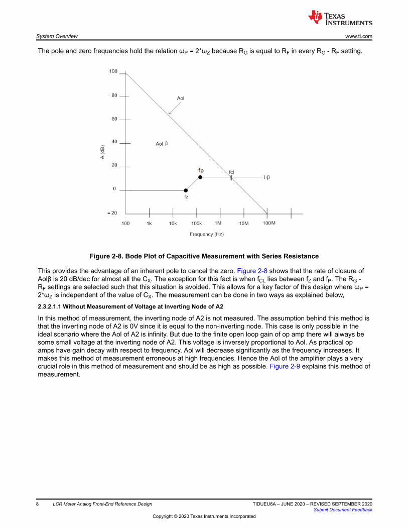
The pole and zero frequencies hold the relation ωP = 2*ωZ because RG is equal to RF in every RG - RF setting.
Figure 2-8. Bode Plot of Capacitive Measurement with Series Resistance
This provides the advantage of an inherent pole to cancel the zero. Figure 2-8 shows that the rate of closure ofAolβ is 20 dB/dec for almost all the CX. The exception for this fact is when fCL lies between fZ and fP. The RG -RF settings are selected such that this situation is avoided. This allows for a key factor of this design where ωP =2*ωZ is independent of the value of CX. The measurement can be done in two ways as explained below,
2.3.2.1.1 Without Measurement of Voltage at Inverting Node of A2
In this method of measurement, the inverting node of A2 is not measured. The assumption behind this method isthat the inverting node of A2 is 0V since it is equal to the non-inverting node. This case is only possible in theideal scenario where the Aol of A2 is infinity. But due to the finite open loop gain of op amp there will always besome small voltage at the inverting node of A2. This voltage is inversely proportional to Aol. As practical opamps have gain decay with respect to frequency, Aol will decrease significantly as the frequency increases. Itmakes this method of measurement erroneous at high frequencies. Hence the Aol of the amplifier plays a verycrucial role in this method of measurement and should be as high as possible. Figure 2-9 explains this method ofmeasurement.
System Overview www.ti.com
8 LCR Meter Analog Front-End Reference Design TIDUEU6A – JUNE 2020 – REVISED SEPTEMBER 2020Submit Document Feedback
Copyright © 2020 Texas Instruments Incorporated

+
±
A1
OPAx810
RG1
RG2
RG3
ZX
+
±
A2
OPAx810
RF1
RF2
RF3
VX
VOUT
Figure 2-9. Method 1 of Impedance Measurement
As this method measures both voltages with respect to ground, data can be acquired using a single-ended ADC.
2.3.2.1.2 With Measuring Voltage at Inverting Node of A2
Figure 2-6 shows the method to measure the difference voltage across both ZX and RF.
This method nullifies the error due to voltage at the inverting node of A2. Since the voltages across ZX and RFare being measured, this method demands a differential ADC be used for data acquisition. In this design, theaccuracies of both methods were verified and found to be the same in the proposed frequencies of operation.High value of Aol (more than 60 dB) of OPA2810 is responsible for this performance.
2.3.2.2 RG = RF Settings and Respective Impedance Ranges
Table 2-1 explains the ranges for different components with respect to the RG - RF and frequency settings.
Table 2-1. Board Setting for Respective Impedance RangePARAMETERS RG = RF SETTINGFrequency (Hz) Component 100 Ω 5 kΩ 100 kΩ100 R 1 Ω to 900 Ω 500 Ω to 50 kΩ 10 kΩ to 10 MΩ
L 1.59 mH to 2.38 H 2.27 H to 79.5 H 72.9 H to 1432 H
C 1.05 µF to 1.59 mF 31.78 nF to 1.11 µF 1.76 nF to 34.7 nF
1 k R 1 Ω to 900 Ω 500 Ω to 50 kΩ 10 kΩ to 10 MΩ
L 159 µH to 238 mH 227 mH to 7.95 H 7.29 H to 143.23 H
C 106 nF to 159 µF 3.178 nF to 111 nF 176 pF to 3.47 nF
10 k R 1 Ω to 900 Ω 500 Ω to 50 kΩ 10 kΩ to 10 MΩ
L 25.9 µH to 23.8 mH 22.6 mH to 795 mH 729 mH to 14.3 H
C 10.6 nF to 15.9 µF 317.8 pF to 11.1 nF 17.6 pF to 347 pF
100 k R 1 Ω to 900 Ω 500 Ω to 50 kΩ 10 kΩ to 10 MΩ
L 2.59 µH to 2.38 mH 2.26 mH to 79.6 mH 72 mH to 1.43 H
C 1.06 nF to 1.59 µF 31.78 pF to 1.11 nF 1.76 pF to 34.7 pF
In the 100 kΩ setting, the parasitic cap at the inverting pin can make the circuit unstable. To overcome thisproblem a 5 pF capacitor is added in parallel with RF = 100 kΩ.
www.ti.com System Overview
TIDUEU6A – JUNE 2020 – REVISED SEPTEMBER 2020Submit Document Feedback
LCR Meter Analog Front-End Reference Design 9
Copyright © 2020 Texas Instruments Incorporated

2.3.2.3 Impedance Measurement Procedure
The impedance measurement procedure includes a one-time calibration procedure which consists of fourdifferent calibrations measurements named as:
1. Short Cal2. Impedance Cal3. 100k Setting Cal4. Open Cal
It must be noted that one time calibrations are done at all four frequencies of operation. Also all the calibratedvalues of RF are phasor quantities and the phase will be used in estimation of the unknown impedance.
2.3.2.3.1 Short Cal
In this calibration, ZX is shorted and the ratio between VO and VIN is measured. This measurement is called asGCAL,
)%#. =81
8+0
(7)
Where VIN is the voltage across RG + ZX. In order to measure VIN, R41 should be removed and a 0-ohm resistoradded to R42. For all other measurements, the default configuration should be used. This calibration is neededonly in RG = RF = 100k setting, as seen in the next steps.
2.3.2.3.2 Impedance Cal
In this calibration, a known resistance of 500 Ω is used as ZX. VO is given by,
81 = lF 4(
500p Û 8+0
(8)
This calibration is used to calculate the exact value of RF, both in the 100 Ω and 5 kΩ settings. It should be notedthat the value of known resistance (RCAL) is selected to be 500 Ω in order to get the best possible calibrationaccuracies in both 100 Ω and 5 kΩ RG = RF settings. User can use other values for RCAL. The accuracy of RCALwill, however, directly affect the calibration accuracy.
2.3.2.3.3 100k Setting Calibration
In this calibration process, the first step is to set RG = 100 kΩ , RF = 5 kΩ and to short ZX. This will give,
)1 = F4(
4)
(9)
With G1 being the measured gain, and RF being the calibrated value of 5kΩ found in the previous step. Usingthis, the calibrated value of RG = 100kΩ can be found. After calibrating for RG = 100 kΩ, we can then use this tocalibrate RF = 100 kΩ using GCAL from the short calibration step. In this way, we have obtained calibrated valuesof RF in all the three settings.
2.3.2.3.4 Open Cal
In this calibration, ZX is kept open. GO is given by,
)1 = F4(
<1
(10)
Where ZO is an open circuit impedance. The significance of this calibration is mainly at higher frequencies whenthe parasitic capacitance in parallel with ZX is large enough to affect the measurement significantly.
System Overview www.ti.com
10 LCR Meter Analog Front-End Reference Design TIDUEU6A – JUNE 2020 – REVISED SEPTEMBER 2020Submit Document Feedback
Copyright © 2020 Texas Instruments Incorporated

2.3.2.3.5 Calculations
To estimate the value of an unknown impedance, Equation 11 can be used. ZX is the unknown impedance, VX isthe voltage across ZX and VO is the voltage across RF.
81
8:
= F4(
<:
(11)
As the calibrated value of RF is known for all settings, ZX can be solved for.
2.3.2.3.6 Correction in ZX
It should be noted that ZX is an effective impedance formed by the parallel combination of an actual unknownimpedance and ZO (Open circuit Impedance). Let the actual value of the unknown impedance be ZX’, then
<: = <1 || <: " (12)
As both ZX and ZO are known, ZX’ can be estimated using Equation 13.
<:"=<1 F <:
<1 Û <:
(13)
Note All the impedances are phasor quantities so the subtraction will be phasor subtraction.
2.3.2.3.7 Data Acquisition and Processing
The voltages are acquired using a two channel differential ADC and processed in the following form. Thefollowing two steps can be implemented in software to obtain the magnitude and phase of any voltage to bemeasured in this application:
1. Modulation of the signal by multiplying the signal with a unity magnitude square wave of 0 degree phase andtaking the average of the resulting signal
2. Modulation of the signal by multiplying the signal with a unity magnitude square wave of 90 degree phaseand taking the average of the resulting signal
2.3.2.3.8 Mathematical Explanation
Let V=VO*Sin(ωt+α) be any signal, if it is multiplied by a unity magnitude square wave with 0° phase then theresultant output is as shown in Figure 2-10.
Figure 2-10. Square Wave Modulation
Let the average value of the output be V1,
www.ti.com System Overview
TIDUEU6A – JUNE 2020 – REVISED SEPTEMBER 2020Submit Document Feedback
LCR Meter Analog Front-End Reference Design 11
Copyright © 2020 Texas Instruments Incorporated

81 = G Û 81 Û %KO:Ù; (14)
Similarly when V is multiplied by square wave with 90° phase, the resultant output is as shown in Figure 2-11.
Figure 2-11. Square Wave Modulation with 90° phase
Let the average value of the output be V2,
82 = G Û 81 Û 5EJ:Ù; (15)
Where k is equal to 4/π.
Using Equation 16 and Equation 17, we get
8 = #RAN=CA KB 8 = §81
2+ 82
22
(16)
= = tanF1 l82
81
p
(17)
In this way, both the magnitude ‘|V|’ and phase ‘α’ of any signal V is estimated.
System Overview www.ti.com
12 LCR Meter Analog Front-End Reference Design TIDUEU6A – JUNE 2020 – REVISED SEPTEMBER 2020Submit Document Feedback
Copyright © 2020 Texas Instruments Incorporated

3 Hardware, Software, Testing Requirements, and Test Results3.1 Required Hardware and Software3.1.1 Hardware
Figure 3-1 and Figure 3-2 illustrate the schematic and board connections of the TIDA-060029 board.
Figure 3-1. Hardware Schematic
www.ti.com Hardware, Software, Testing Requirements, and Test Results
TIDUEU6A – JUNE 2020 – REVISED SEPTEMBER 2020Submit Document Feedback
LCR Meter Analog Front-End Reference Design 13
Copyright © 2020 Texas Instruments Incorporated

Figure 3-2. Board Connections
Table 3-1. Connector DetailsCONNECTOR DESCRIPTIONJ1, J2, J3, J5, J7, J10 RG = RF Settings connectors
J6 Offset Calibration connector
J14 Offset Cal Connector
J15 OPA2810 Supply
J20 BUF634 Supply
J16 VCA 821 Supply
J17, J18 Jumpers between J15 and J20
J9 Input Connector
J12, J13 VX Measurement Connectors
J8, J11 VOUT Measurement Connectors
Hardware, Software, Testing Requirements, and Test Results www.ti.com
14 LCR Meter Analog Front-End Reference Design TIDUEU6A – JUNE 2020 – REVISED SEPTEMBER 2020Submit Document Feedback
Copyright © 2020 Texas Instruments Incorporated

3.2 Testing and Results3.2.1 Test Setup
1. Short the jumper J6. It should be noted that jumper J6 is for offset calibration and not used in this design.2. Always keep one of the jumpers among J1, J2, J3 short according to RG – RF setting needed. This prevents
the saturation of U2A.3. Connect both +/- 12 V and +/-15 V power supplies to J15 and J20 respectively.4. Set the required RG – RF setting, refer to Table 2-1 and Table 3-2 to determine and set desired connections.5. Do calibration of each setting at all 4 frequencies according to the calibration process explained in Section
2.3.2.3. Use Table 3-2 to make connections according to required calibration.6. Use the calibration results to estimate the unknown impedance as explained in Section 2.3.2.3.
Configurations for different connections on the board are given inTable 3-1
Table 3-2. Connector ConfigurationsCONDITION CONNECTOR CONFIGURATIONShort Calibration J6 = Short, R41 = Open, R42 = Short
Open Calibration J6 = Open
ImpedanceCalibration
J6 = Open
RG = RF =100Setting
J1 J2 J3 J5 J7 J10
Short Open Open Short Open Open
RG = RF =5 kSetting
J1 J2 J3 J5 J7 J10
Open Short Open Open Short Open
RG = RF =100 kSetting
J1 J2 J3 J5 J7 J10
Open Open Short Open Open Short
Table 3-3 provides recommended operating voltages on connectors.
Table 3-3. Operating VoltagesDESCRIPTION RECOMMENDED VOLTAGEOPA2810 Supply (J15) +/- 12 V
BUF634A Supply (J20) +/- 15 V
VCA Supply (J16)(NOT USED) +/- 5 V
3.2.2 Test Results
The following example shows the unknown capacitive impedance measurement in detail.
Component : C = 100 nF
Measured value of the C = 99.472 nF
Frequency of Test = 1 kHz
RG = RF Setting = 100 Ω
Calibrated value of RF = 99.97686
RF/ZX = 0.062412398 and α = 90.125° ( phase of the ratio)
Thus, ZX = 1601.875005 and θX = 90.125°
:% = <: Û 5EJ:àT; (18)
:% = 1601.875 Û sin:F90.125; (19)
www.ti.com Hardware, Software, Testing Requirements, and Test Results
TIDUEU6A – JUNE 2020 – REVISED SEPTEMBER 2020Submit Document Feedback
LCR Meter Analog Front-End Reference Design 15
Copyright © 2020 Texas Instruments Incorporated

:% = 1599.99 (20)
% =1
2 Û è Û B Û :%
(21)
Using Equation 21 we get, C = 99.3556 nF
% 'NNKN =:99.472 F 99.356; Û 100
99.472
(22)
Thus the % Error = 0.116 %
All other components are measured in the same way. The results are shown in Table 3-4.
It should be noted that the errors are estimated with respect to the value estimated by Keysight Technologies’E4980A precision LCR Meter. For testing, an input of 3.6 Vpp was used and results were measured with aseperate board utilizing the THS4551 and ADS9224R.
Table 3-4. Board Measurement ResultsParameters RG = RF SettingFrequency (Hz) Component 100 Ω Error(%) 5 kΩ Error(%) 100 kΩ Error(%)100 R 1 Ω – 900 Ω 0.74 500 Ω – 50 kΩ 0.11 10 kΩ – 10 MΩ 0.3
L 1.59 mH – 2.38H
1.18 2.27 H – 79.5 H - 72.9 H – 1432H
-
C 1.05 µF – 1.59mF
3 31.78 nF - 1.11µF
0.62 1.76 nF - 34.7nF
0.36
1k R 1 Ω – 900 Ω 0.72 500 Ω – 50 kΩ 0.12 10 kΩ – 10 MΩ 0.56
L 159 µH – 238mH
0.47 227 mH – 7.95H
- 7.29 H – 143.23H
-
C 106 nF – 159µF
0.12 3.178 nF – 111nF
0.39 176 pF – 3.47nF
0.1
10k R 1 Ω – 900 Ω 0.71 500 Ω – 50 kΩ 0.12 10 kΩ – 10 MΩ 2.49
L 25.9 µH – 23.8mH
0.57 22.6 mH – 795mH
1.81 729 mH – 14.3H
-
C 10.6 nF – 15.9µF
0.94 317.8 pF – 11.1nF
0.4 17.6 pF – 347pF
0.22
100k R 1 Ω – 900 Ω 0.47 500 Ω – 50 kΩ 0.87 10 kΩ – 10 MΩ 14
L 2.59 µH – 2.38mH
0.71 2.26 mH – 79.6mH
4.8 72 mH – 1.43 H -
C 1.06 nF – 1.59µF
0.17 31.78 pF - 1.11nF
1.8 1.76 pF- 34.7pF
5.5
Hardware, Software, Testing Requirements, and Test Results www.ti.com
16 LCR Meter Analog Front-End Reference Design TIDUEU6A – JUNE 2020 – REVISED SEPTEMBER 2020Submit Document Feedback
Copyright © 2020 Texas Instruments Incorporated

4 Design Files4.1 SchematicsTo download the schematics, see the design files at TIDA-60029.
4.2 Bill of MaterialsTo download the bill of materials (BOM), see the design files at TIDA-60029.
4.3 PCB Layout RecommendationsThis design follows the guidelines found in the Layout section of the OPA2810 data sheet.
4.3.1 Layout Prints
To download the layer plots, see the design files at TIDA-60029.
4.4 Altium ProjectTo download the Altium Designer® project files, see the design files at TIDA-60029.
4.5 Gerber FilesTo download the Gerber files, see the design files at TIDA-60029.
4.6 Assembly DrawingsTo download the assembly drawings, see the design files at TIDA-60029.
5 Software FilesTo download the software files, see the design files at TIDA-60029.
6 Related Documentation1. Texas Instruments, OPA2810 Dual-Channel, 27-V, Rail-to-Rail Input/Output FET-Input Operational Amplifier
data sheet2. Texas Instruments, BUF634A 36-V, 210-MHz, 250-mA Output, High-Speed Buffer data sheet
6.1 TrademarksTI E2E™ is a trademark of Texas Instruments.Altium Designer® is a registered trademark of Altium LLC or its affiliated companies.All other trademarks are the property of their respective owners.6.2 Third-Party Products DisclaimerTI'S PUBLICATION OF INFORMATION REGARDING THIRD-PARTY PRODUCTS OR SERVICES DOES NOTCONSTITUTE AN ENDORSEMENT REGARDING THE SUITABILITY OF SUCH PRODUCTS OR SERVICESOR A WARRANTY, REPRESENTATION OR ENDORSEMENT OF SUCH PRODUCTS OR SERVICES, EITHERALONE OR IN COMBINATION WITH ANY TI PRODUCT OR SERVICE.
Revision HistoryNOTE: Page numbers for previous revisions may differ from page numbers in the current version.
Changes from Revision * (June 2020) to Revision A (September 2020) Page• Changed Capacitive Measurement with Series Resistance image.................................................................... 7• Changed Square Wave Modulation image....................................................................................................... 11
www.ti.com Design Files
TIDUEU6A – JUNE 2020 – REVISED SEPTEMBER 2020Submit Document Feedback
LCR Meter Analog Front-End Reference Design 17
Copyright © 2020 Texas Instruments Incorporated

IMPORTANT NOTICE AND DISCLAIMER
TI PROVIDES TECHNICAL AND RELIABILITY DATA (INCLUDING DATASHEETS), DESIGN RESOURCES (INCLUDING REFERENCE DESIGNS), APPLICATION OR OTHER DESIGN ADVICE, WEB TOOLS, SAFETY INFORMATION, AND OTHER RESOURCES “AS IS” AND WITH ALL FAULTS, AND DISCLAIMS ALL WARRANTIES, EXPRESS AND IMPLIED, INCLUDING WITHOUT LIMITATION ANY IMPLIED WARRANTIES OF MERCHANTABILITY, FITNESS FOR A PARTICULAR PURPOSE OR NON-INFRINGEMENT OF THIRD PARTY INTELLECTUAL PROPERTY RIGHTS.These resources are intended for skilled developers designing with TI products. You are solely responsible for (1) selecting the appropriate TI products for your application, (2) designing, validating and testing your application, and (3) ensuring your application meets applicable standards, and any other safety, security, or other requirements. These resources are subject to change without notice. TI grants you permission to use these resources only for development of an application that uses the TI products described in the resource. Other reproduction and display of these resources is prohibited. No license is granted to any other TI intellectual property right or to any third party intellectual property right. TI disclaims responsibility for, and you will fully indemnify TI and its representatives against, any claims, damages, costs, losses, and liabilities arising out of your use of these resources.TI’s products are provided subject to TI’s Terms of Sale (www.ti.com/legal/termsofsale.html) or other applicable terms available either on ti.com or provided in conjunction with such TI products. TI’s provision of these resources does not expand or otherwise alter TI’s applicable warranties or warranty disclaimers for TI products.
Mailing Address: Texas Instruments, Post Office Box 655303, Dallas, Texas 75265Copyright © 2020, Texas Instruments Incorporated