Embed Size (px)
Citation preview

Lavinia P. Rajahram
18th April 2014
NANO LASER

SHRINKING THE LASER!

A BRIEF OVERVIEW
An oscillator comprises:• Amplifier with gain-saturation mechanism• A feedback system• A frequency-selection mechanism• Output coupling scheme
SUB-WAVELENGTH DIMENSIONS!

NANO LASER - BACKGROUND• Concept developed by Mark Stockman in 2003 at Georgia State University. Theory is
based on electron vibration rather than the traditional electron excitation
• These vibrating electrons (called nanopendulums or plasmons) were not seen as of 2003.
• In 2009, after almost 50 years of laser invention, Surface Plasmon Amplification by Stimulated Emission of Radiation(SPASER) was achieved.
• To act like lasers a feedback system was required for the Surface Plasmon to oscillate back and forth so that they gain power and can be emitted as light

SPASER (2009)
• Photons replaced by Surface Plasmon
• Resonant cavity replaced by Nanoparticles
• Energy source active gain medium excited externally

PHOTON SURFACE PLASMON
• 44nm nanoparticle with gold core and dye doped silica shell
• Surface plasmon resonance capable of squeezing optical frequency

SPASER BASED NANOLASER
Nature, 27 August 2009
Induced Radiation Rate or Excitation Rate depending on its
sign!
LASING IN METAMATERIAL NANOSTRUCTURES
• Gain described by generic 4 level atomic system• Critical pumping rate to compensate losses in
nanostructure
Journal of Optic, Jan 2010
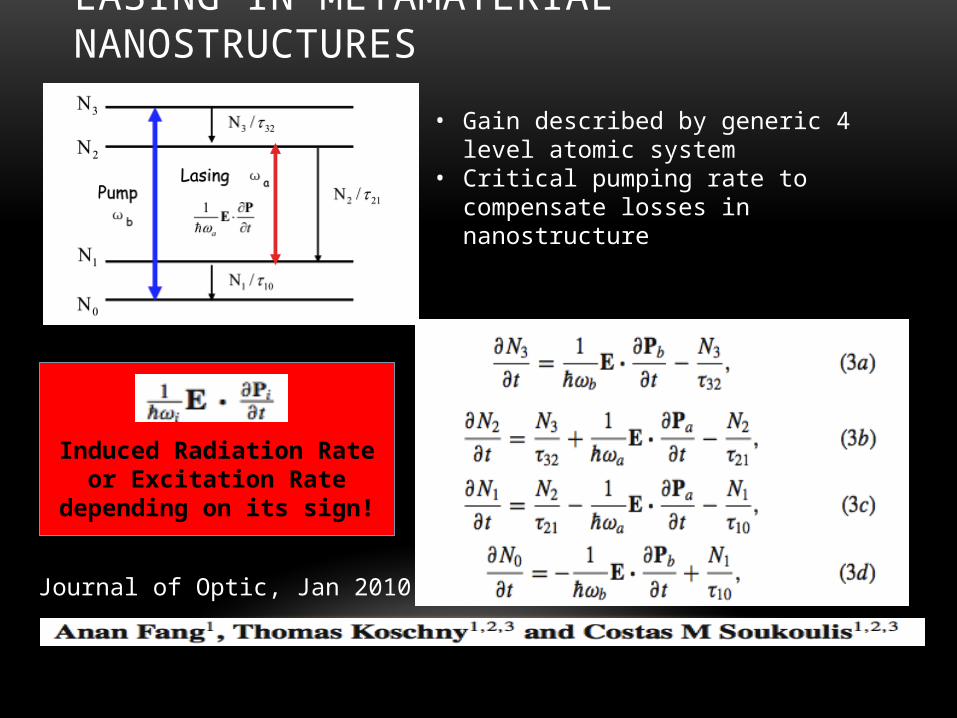
LASING IN METAMATERIAL NANOSTRUCTURE

MY CURRENT RESEARCH
• To understand fundamental properties of spontaneous emission altered by metamaterial
• To understand the coupled nanostructure gain system (dealing with time dependent wave equations in metamaterial)
• Coupling Maxwell’s equation with the Rate equation of electron populations
• Starting with a 3 level atomic system code with FDTD formalization
• Understanding parallel simulations

3 LEVEL SYSTEM
• Maxwell + Rate Equation• Atomic transition dipole• Forth order Runge - Kutta Method• Finite – Difference Time Domain Method
(FDTD)
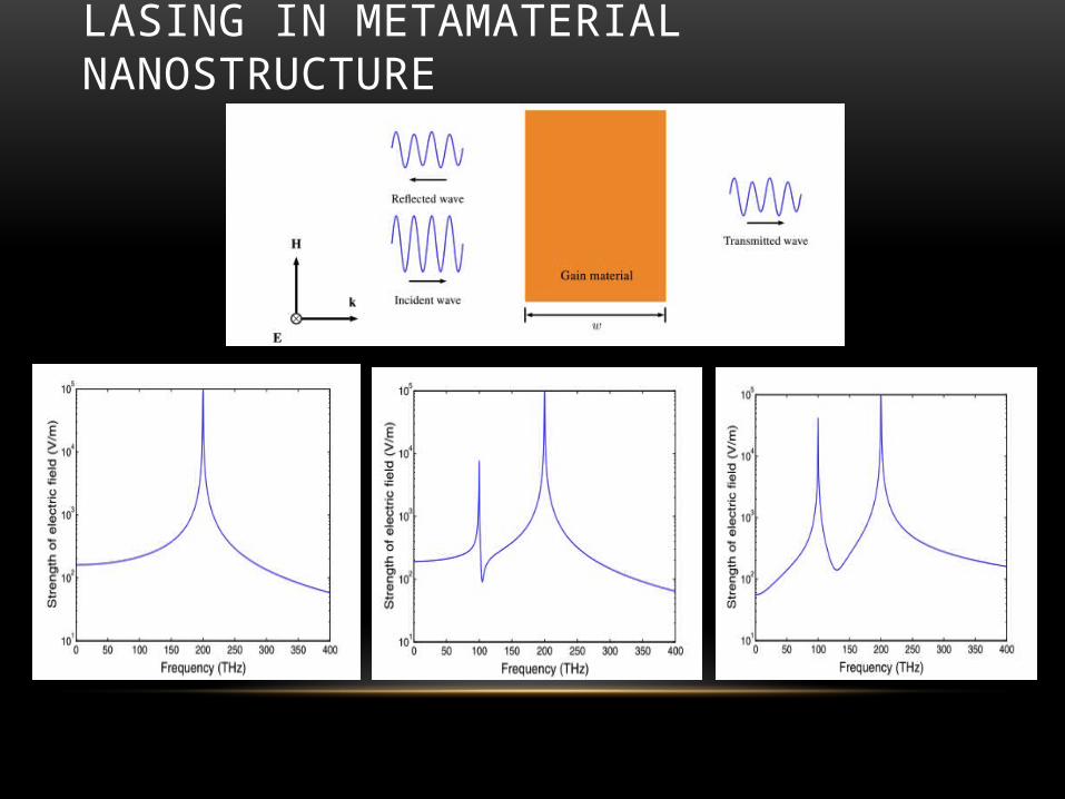
PARALLEL COMPUTATION
R1 = 20.25nm
R2 = R1 + 10.25nm
NX = 231
N Y = 3
21
• Each rank has 20 grid• No of processor 16• Scattered field zone at Rank 12
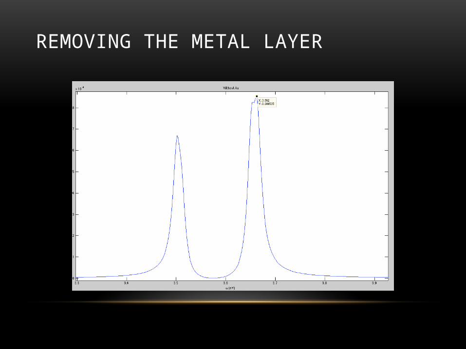
REMOVING THE METAL LAYER

REMOVING DYE/MOLECULES LAYER

COMPLETE MODEL

VARYING THE THICKNESS OF METAL