Embed Size (px)
Citation preview

7-1
LAB VI. TRANSIENT SIGNALS OF PN JUNCTION DIODES
1. OBJECTIVE
In this lab, you are to study the transient effects in a p-n junction diode due to a sudden
large change in current. Pn junction diodes allow one to change the current flowing through them
almost instantaneously, but they will NOT allow one to change the voltage across them
instantaneously. As a result, a phenomenon called “charge storage delay” can allow large reverse
bias currents to flow through a diode for short periods of time.
2. OVERVIEW
In the previous lab, we assumed that the stored charge density in the n-side and p-side
regions of our diode did not significantly change as a small signal was applied. In other words,
we assumed that the diode is in steady-state even though we apply “small” ac signals. We will
now apply large change in the voltage and current and use a charge control analysis to make a
first order approximation of the current and voltage values of the diode as a function of time.
This knowledge can be used in understanding the switching processes of a p-n junction diode.
Information essential to your understanding of this lab:
1. Carrier injection and storage (Streetman section 5.3.2)
2. Transient and AC conditions (Streetman sections 5.5.1~5.5.3)
Materials necessary for this Experiment:
1. Standard testing station
2. One rectifier diode (Part: 1N4002)
3. 10 Ω, 2W resistor (Resistance substitution box, Elenco model RS-400)
3. BACKGROUND INFORMATION
3.1 CHART OF SYMBOLS
Here is a chart of symbols used in this lab manual. This list is not all inclusive; however,
it does contain the most common symbols and their units used in this Lab.
Table 1. Chart of the symbols used in this lab.
Symbol Symbol Name Units
h+ Hole Positive charge particle
e- electron Negative charge particle
q magnitude of electronic charge 1.6 x 10⁻¹⁹
C
p hole density (number h+ / cm
2)
n electron density (number e- / cm
2)
ni intrinsic electron density (number e- / cm
2)
p hole concentration at depletion edge (number h+ / cm
2)
n electron concentration at depletion edge (number e- / cm
2)
kb Boltzmann's constant 1.38 x 10⁻²³
joules / K
T Temperature K
Eg energy gap of semiconductor eV
A junction area cm2

7-2
g general carrier lifetime
sec
p hole lifetime sec
n electron lifetime sec
Lp diffusion length of holes cm
Ln diffusion length of electrons cm
xp x-axis for p-type material cm
xn x-axis for n-type material cm
I0 reverse saturation current A
I change in DC current A
VD DC diode voltage V
vd AC diode voltage V
vD total diode voltage V
tfr forward recovery time sec
trd relaxation delay time sec
tsd storage delay time sec
trr reverse recovery time sec
3.2 CHART OF EQUATIONS
All of the equations from the background portion of the manual are shown in the table
below.
Table 2. Chart of the equations used in this lab. Equation
Name Formula
1 Ideal Diode Equation 1)()/)((
0 nkTtqV
DDeItI
2 Hole current in a p+n
junction as a function of the stored charge Qp
dt
tdQtQti
p
p
p
p
)()()(
3 Stored charge in the n-side as a function of time tpqALeItQ np
t
pFpp
)(
4 Excess charge carrier concentration at the edge of the depletion region in the n-side
1)( 0
kT
tqv
n
p
p
n epqAL
tQtp
5 Voltage across the p+n
junction assuming quasi-steady state conditions
1ln)(0
p
t
np
pFe
pqAL
I
q
kTtv
3.3 TIME DEPENDANCE OF THE IDEAL DIODE EQUATION
When the voltages applied over the p-n junction diode vary over time, the diode currents
are time dependent. When the current and the junction voltage changes slower than the diffusion
of minority carriers, diode will maintain the quasi-steady state conditions and the I-V relation of
the p-n junction diode is given by:

7-3
1)()/)((
0 nkTtqv
DDeIti . (1)
What if the current and voltage signals change over time much faster than the change of the
minority carrier re-distribution? Since it takes time for the re-distribution of minority carriers, as
a result the I-V characteristic cannot be represented by (1).
Figure 1 shows the re-distribution of minority carriers with time as a function of the
position in the n-side when the current flow through a p+-n junction diode suddenly stops (a turn-
off transient). As soon as the current stop flowing, there will be no more hole diffusion from the
p-side and the stored charge distribution decays exponentially in time but does not decay
exponentially in space. Recall that the charge density at the depletion edge is proportional to the
current flow. If the current flow is zero then the slope of the charge density at the depletion edge
must be zero (Figure 1).
Figure 1. A turn-off transient: current as a function of time (left) and minority carrier re-
distribution over time as a function of position in the n-side (right).
The distortion of the steady state exponential curve in space makes it difficult to directly
calculate the stored charge as a function of time. Therefore, we will utilize quasi-steady state
approximations to get simplified solutions for the characteristics of the p-n junction diode. In a
quasi-steady state approximation, the decay of a stored charge is assumed to maintain the same
exponential form in space as the steady state condition. Using this approximation, we can
calculate rather simply the stored charge in time and find the voltage across the junction.
Examine Figure 2 for a graphical example of the quasi-steady state approximation.
Now consider a turn on transient. In this case, the current is suddenly stepped up from
zero to IF. For t > 0+, the increased hole injection current will first cause an increase in the excess
hole density at the edge (xn0) of the depletion region. Shortly after, the excess holes will have had
time to diffuse into the neutral region of the n-side, thus increasing the charge stored in the n-side
as shown in Figure 3. The diffusion process takes time and the build-up of charge will always lag
the build-up of the charge near x = 0. During the transient, the total diode current is the sum of
the recombination current, and the charge build up current, yielding:
dt
tdQtQti
p
p
p
p
)()()(
. (2)
xn
0 t1 t2
0t
01 tt
12 ttt
ID δp(xn)
t
Iforward
Notice how the slope is zero at the depletion edge.
DC steady state charge density level

7-4
Figure 2. Excess carrier concentration as a function of position in time: the dotted lines are the
actual carrier distributions while the solid lines are quasi-steady state charge approximations.
Figure 3. A turn-on transient: current as a function of time (left) and minority carrier re-
distribution over time as a function of position in the n-side (right).
3.4 CHARGE CONTROL ANALYSIS
In many cases, we will know the current running through a diode and can use it to find
the stored charge in a p-n junction diode. After finding the stored charge, it is possible to find the
charge density at the depletion region edge which can be used to calculate the voltage across the
junction as a function of time. To find the stored charge we will use Laplace transforms on the
equation (2) to solve for the stored charge Q(t).
For generality, we are going to use IF + I as our current at time equal to zero, where IF is the
initial current which has established a steady state charge, and I is the change in current that is
either positive or negative, and can be a time varying function. Take the Laplace transform of the
equation (8). You can use the initial condition for the charge density (Q(0) = Ip) to solve the
equation. After algebraic manipulation and the reverse Laplace transform you will find that:
tpqALeItQ np
t
pFpp
)( (3)
Then, the excess charge carrier concentration at the edge of the depletion region is:
0t
01 tt
12 ttt
δp(xn)
Notice the difference in the dotted lines(actual charge densities) and the solid lines(quasi-steady state approximations).
Steady state condition excess charge carrier distribution
quasi-steady state approximations
xn
0 t1 t2
01 tt
12 ttt
ID δp(xn)
t
IF
Notice how the slope of the blue line is the same as that of the line for time less than zero.
xn
at steady state
7-5
1)( 0
kT
tqv
n
p
p
n epqAL
tQtp (4)
If you solve for v(t), then you will get:
1ln)(0
p
t
np
pFe
pqAL
I
q
kTtv
(5)
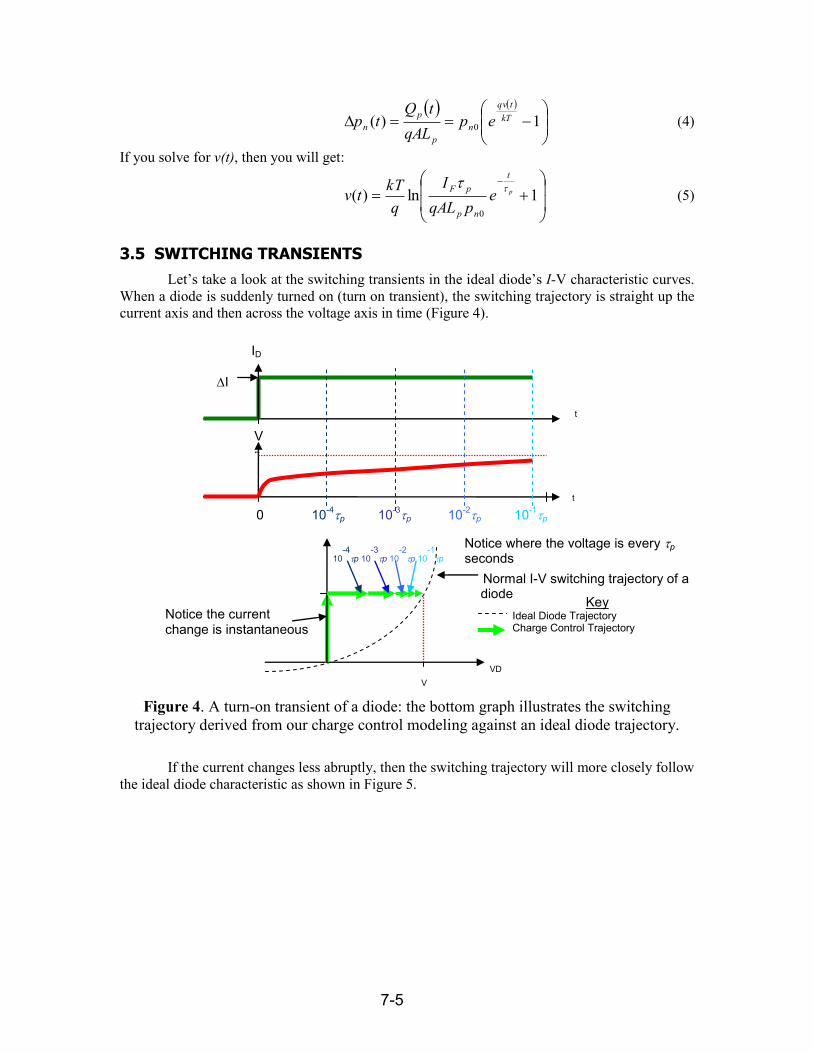
3.5 SWITCHING TRANSIENTS
Let’s take a look at the switching transients in the ideal diode’s I-V characteristic curves.
When a diode is suddenly turned on (turn on transient), the switching trajectory is straight up the
current axis and then across the voltage axis in time (Figure 4).
Figure 4. A turn-on transient of a diode: the bottom graph illustrates the switching
trajectory derived from our charge control modeling against an ideal diode trajectory.
If the current changes less abruptly, then the switching trajectory will more closely follow
the ideal diode characteristic as shown in Figure 5.
t
I
0 10-4p 10
-3p 10
-2p 10
-1p
t
V
D
ID
I
D
VD
Notice the current change is instantaneous
I
Key Ideal Diode Trajectory Charge Control Trajectory
10-4p 10
-3p 10
-2p 10
-1p
V
Normal I-V switching trajectory of a diode
Notice where the voltage is every p
seconds

7-6
VS(t) vD(t)
R
- iD(t) +
+
-
+
-
Figure 5. The switching trajectory for different turn-on transient conditions.
3.6 TIME DELAYS INCURRED BY SWITCHING
Now that you have some idea of what a switching trajectory is and how it works, we are
going to look at a slightly more complex circuit with a voltage signal, a series resistance, and a
diode configured as shown in Figure 6. The purpose in doing so is to find out how long it takes
for our switching operation to take place and reach to the desired level. This information is useful
to see how fast a diode can switch. The switching speed of a diode is important because in most
practical applications, diodes are used in ac applications rather than dc applications.
Figure 6. A circuit diagram for the time delay measurement.
When a step on voltage is applied to a p-n junction with a series resistance you should have an
output similar to Figure 7. Notice that the voltage across the junction spikes and then settles
down to a steady state voltage level. When the voltage across the diode has dropped to within
10% of the steady state value the junction is said to have recovered. The forward recovery time,
tfr is the time from the switching on of the voltage source to the time that diode has recovered.
When a voltage source is turned off, the stored charge is present until it recombines or is
dissipated over the resistor in the circuit. We will give this type of charge storage delay a special
name, the relaxation delay time, trd (Figure 8). We state that the system is relaxed if it’s current
value is within 10% of the steady state value.

7-7
Figure 7. A turn on transient: the graph above shows applied voltage waveform (step
function) from the function generator and the bottom graph shows corresponding voltage
signal across the diode. Note how to determine the tfr.
Figure 8. A turn off transient: the graph above shows applied voltage waveform from the
function generator and the bottom graph shows corresponding voltage signal across the
diode. Note how to determine the trd.
Voltage (off)
Cut off point for voltage signal
t
trd
t
0
VD
VS(t)
Steady state voltage
V = 0.1(Steady State Voltage – Voltage(off))
Voltage dropped over the resistor.
0
Can grow to the step on voltage
t
V
tfr
t
VD
VS(t)
Voltage Peak
Steady State Voltage
V = 0.1(Voltage Peak – Steady State Voltage)
Charge builds until the Diode turns on

7-8
When you switch from forward to reverse bias (“a positive to negative transient” or a
“reverse recovery transient”) reverse recovery switching will occur as shown in Figure 9. Figure
9 a) depicts the case of an ideal current source which is stepped from a forward biasing current IF
to a current of opposite polarity. Since IF is assumed to be flowing for quite some time we should
expect to see a steady state charge density at t=0.
Figure 9. Reverse recovery switching trajectories for a current source (a) and a voltage
source (b).
Now when t=0+, the slope of the charge distribution must change so that its slope
matches that of the current that is flowing. The reverse current consists of minority carrier being
drawn back across junction into the p-type material. The charge density in n-side is shown in
Figure 10.
Δp(xn)
Figure 10. Changes in the excess charge carrier distribution over time. Note the positive
slopes near the edge of the depletion region.

7-9
When the stored charge density on both sides of the junction reaches zero, the storage delay
portion of the transient is over. The current supply will then rapidly drive the diode into reverse
breakdown. In the case of a voltage source, Figure 9 b), the current supplied to the circuit can be
approximated as the voltage supplied by the source over the series resistance. This means that the
current sourced is dependent on the voltage dropped across the resistor. After the storage delay
time (tsd), the diode turns off changing the diodes role in the circuit from that of a simple voltage
drop to impedance many orders of magnitude larger than that of the resistor causing nearly all the
voltage to fall across the p-n junction. Notice that the voltage dropped across the resistor dies
away exponentially in time. Since the current for the circuit is the same as that flowing through
the resistor, the exponential drop in voltage causes the reverse current to die away to the reverse
saturation current.
The total reverse recovery time (trr) is the time it takes the voltage signal across
the diode to rise to 10% of the steady state value from the reverse voltage experienced by
the diode during the storage delay period. Figure 11 demonstrates both the storage delay
time tsd, and the reverse recovery time, trr.
Figure 11. A reverse recovery transient of a diode. Note the time period of each delay on
the time axis.
t
vF
trd
t
vResistor(t)
VS(t)
Voltage Peak
Steady State Voltage
V = 0.1(Voltage Peak – Steady State Voltage)
vR
trr
tsd

7-10
4. PREPARATION
1. Make sure you understand how to properly operate the oscilloscope by reading the
section 3.3 of the Lab 2 manual. Outline section 3.3 of the Lab 2 manual.
2. Outline sections 3.3 to 3.6 of this Lab 6 manual. Take note of key assumptions and main
concepts contained in each section.
5. PROCEDURE The following measurements will be made using your rectifier diode (1N4002). Since
there will be substantial currents flowing at various times in the experiment be sure to use a 10 ,
2W resistor (Resistance substitution box, Elenco model RS-400) for this experiment. In this Lab,
you need to manually control the function generator and the oscilloscope to get the data.
5.1 TURN ON TRANSIENT In this section, you are about to measure the forward recovery transient of the diode voltage as the
pulsed current is switched on from I = 0 to I = IF as a function of IF.
1. Turn the knob of the Elenco model RS-400 to 10 Ω. Measure the exact value of your ~10
Ω resistor using the Keitheley SMU and record it in the Table 3. You will need exact
resistance value to accurately analyze the data of Lab 6.
2. Construct the circuit as shown in Figure 12.
3. Program the function generator to output a square wave. In this lab, we’ll use the “High-
Level” and “Low-Level” settings on the function generator rather than the “Amplitude”
and “Offset” settings. Set the function generator to have a high-level voltage of 1 V and
a low-level voltage of 0 V. We choose the low-level to be 0 V because we need a step
function rather than a square wave in this part of the experiment. This generates a 1V
u(t) step function output from the function generator. Set the frequency of the function
generator at 20 kHz. Do not change the duty cycle (default value is 50 %).
4. If you are not sure how to operate the oscilloscope, go back to the Lab 2 manual and
read more on the oscilloscope operation. Measure the forward current (IF) as follows and
record it in the Table 3.
R
VVI
ssChssCh
F
,1,2 ,
where the subscript ss represent steady state. You can see a close up view of the
waveforms similar to that in Figure 7.
5. Use scopegrab.vi to collect data.
6. Now turn the channel 2 off and leave only the channel 1 on. Use the cursors for both
voltage and time to find the Vpk - Vss and the forward recovery time (tfr) as shown in
Figure 7. Record the forward recovery time in the Table 3.
7. Again, use scopegrab.vi to collect data.
8. You have to repeat this experiment with various high-level step voltages (1~5 V) and
record IF and tfr. See Table 3 below.

7-11
Figure 12. Circuit used to make the turn on and turn off transient measurements.
Table 3. Measured data for the turn on and turn off transient.
VHigh-Level VLow-Level R IF Vpk-Vss tfr Vss-Voff trd
1 V + 0.0 V
2.5 V + 0.0 V
5 V + 0.0 V
5.2 TURN OFF TRANSIENT
Next, you are about to measure the turn off characteristic of the p-n junction diode.
1. Use the same circuit and the same input as used in the previous section (5.1), but this
time you would see the close up view of the waveforms similar to the Figure 8.
2. Use the channel 1 to measure the Vss – Voff and relaxation delay time (trd) and record it in
Table 3 above. Again, repeat the experiment for all 3 voltages shown in the Table 3 and
use scopegrab.vi to collect data for graphs for each measurement.
5.3 REVERSE RECOVERY TRANSIENT
Next, you are about to measure the forward and reverse current and reverse recovery transient of
the diode as the pulsed current is switched from IF to IR.
1. Construct the circuit as shown in Figure 13.
2. Program the function generator to output a square wave. Set the function generator to
have a high-level voltage of 0.9 V and a low-level voltage of 0 V. Set the frequency of
the function generator to 20 kHz. Do not change the duty cycle (default value is 50 %).
3. Measure the forward current (IF) and the reverse current (IR) as follows and record
them in the Table 4. You would see the close up view of the waveforms similar to the
Figure 11.
R
VI Ch1 .
4. Now use the cursors for both voltage and time to find the storage delay time (tsd) and the
total reverse recovery time (trr) as shown in Figure 11 and record them in the Table 4.
5. Use scopegrab.vi to collect data.
6. Again, you have to repeat this experiment with several different voltage settings as shown
in Table 4 and record tsd and trr.
1N4002

7-12
Figure 13. Circuit used to make the reverse recovery transient measurements.
Table 4. Measured data for the reverse recovery transient.
VHigh-Level VLow-Level VF IF VR IR tsd trr
0.9 V 0.0 V
0.9 V - 0.5 V
0.9 V -1 V
0.9 V -2 V
0.9 V -4 V
0.5 V -1 V
0.1 V -1 V
1.4 V -1 V
1.8 V -1 V
6. LAB REPORT
Write a summary of the experiment.
Turn ON Transient
o Include your Table 3 data with the values you recorded in it.
o Using any one particular data set (e.g., 1V High-Level and 0V Low-Level), properly
plot the voltage waveforms from both channels and show how you calculated the
forward current IF. You should import your graph into your report and use labels to
show Vch1,ss and Vch2,ss.
o Again, using any one particular data set, properly plot the CH1 voltage waveform and
show how you calculate the forward recovery time tfr. You should import your graph
into your report and use labels to show Vpeak and Vss.
o In your own words, briefly explain what is happening in the diode during this turn on
transient.
Turn OFF Transient
o Make sure to present all Turn OFF Transient data in Table 3 in addition to the Turn
ON Transient.
o Using any one particular data set (e.g., 1V High-Level and 0V Low-Level), properly
plot the CH1 voltage waveform and show how you calculated the relaxation delay
1N4002

7-13
time trd. You should import your graph into your report and use labels to show Vss
and Voff.
o In your own words, briefly explain what is happening in the diode during this turn off
transient.
Reverse Recovery Transient
o Include your Table 4 data with the values you recorded in it.
o Using any one particular data set (e.g., 0.9V High-Level and -0.5V Low-Level),
properly plot the voltage waveform from CH1 to show VF, VR, tsd, and trr. You should
import your graph into your report and use labels to show VF, VR, tsd, and trr.
o In your own words, briefly explain what is happening in the diode during this reverse
recovery transient.
If you have taken any extra credit data for other devices, repeat the above for each
device.