Embed Size (px)
Citation preview
LAB 6: BJT AMPLIFIER
LEARNING OUTCOMES:
In this lab, students design and implement single-stage BJT amplifiers and observe
amplitude and frequency response. Breadboard and the Analog Discovery Kit are to be
used. The students will use various tools and functions from the Waveform software to
perform measurement and plotting amplifier response. The students will compare the gain
and frequency response of the BJT amplifier and the MOSFET amplifier in Lab 5.
MATERIAL AND EQUIPMENT
Material Equipment
2N2222 npn BJT transistor Breadboard
Capacitors Multimeter
Resistors Analog Discovery
2N2907 pnp BJT transistor Digilent Waveform software
Curve tracer
PRE-LAB
Look at the handout and be familiar with the CE amplifier. You need to know how to
calculate the DC voltage, current and small-signal gain. Design an amplifier with a voltage
gain of -4, a collector current of 5 mA, bias the collector voltage to provide a maximum
output voltage swing (i.e., ½ of Vcc). Use a Vcc of +5 V from the power supply of the
Analog Discovery unit.
PROCEDURES
1. NPN transistor characteristics
Obtain 2N2222 Si npn from the lab instructor or from the technician in room 2C97. Measure
their βDC at VCE =5V using the Tektronix curve tracers. Use a scale of 0 - 10 mA for IC and 0
- 10 V for VCE. The step current for the base is 10uA. You need to capture the transistor
characteristics to your lab report. Label βDC on the curves. The normal βDC of 2N2222 is
between 100-200. Also use the information in Lab 5 BJT IV curve.
2. Common-Emitter amplifier
Construct the circuit shown in Figure 1. You can use either 1 uF for capacitor CB and 4.7 uF
for the capacitor CC.
A. Measure the DC currents and voltages: IB, IC, IE, VC, VB, VE. Remember to measure one
at a time and NO input AC signal. In your report, make a table and list the results from
your experiment and hand calculations. In your hand calculation, use β determined from
your IV curve. Assume VBE = 0.7V.

2
B. At this time, do NOT connect the load resistor RL yet. Generate an input signal from
AWG1 (100 mVpp, 1 KHz) and send the signal to the input of the amplifier. Observe the
input and output voltage waveforms using two probes of an oscilloscope (Channel 1 and
Channel 2). First observe the waveforms of the input signals that are before and after CB.
Note that how DC voltage at the base is preserved by using coupling capacitor. Then
observe the waveforms of signals Vc and Vo that are before and after CC. The waveform
at Vc has both AC and DC components and waveform at Vo is a pure AC signal because
of the coupling capacitor CC. Capture the waveforms at Vi, VB, Vc and Vo copy them to
your lab report. Find the voltage gain from the waveforms (Vo/Vi).
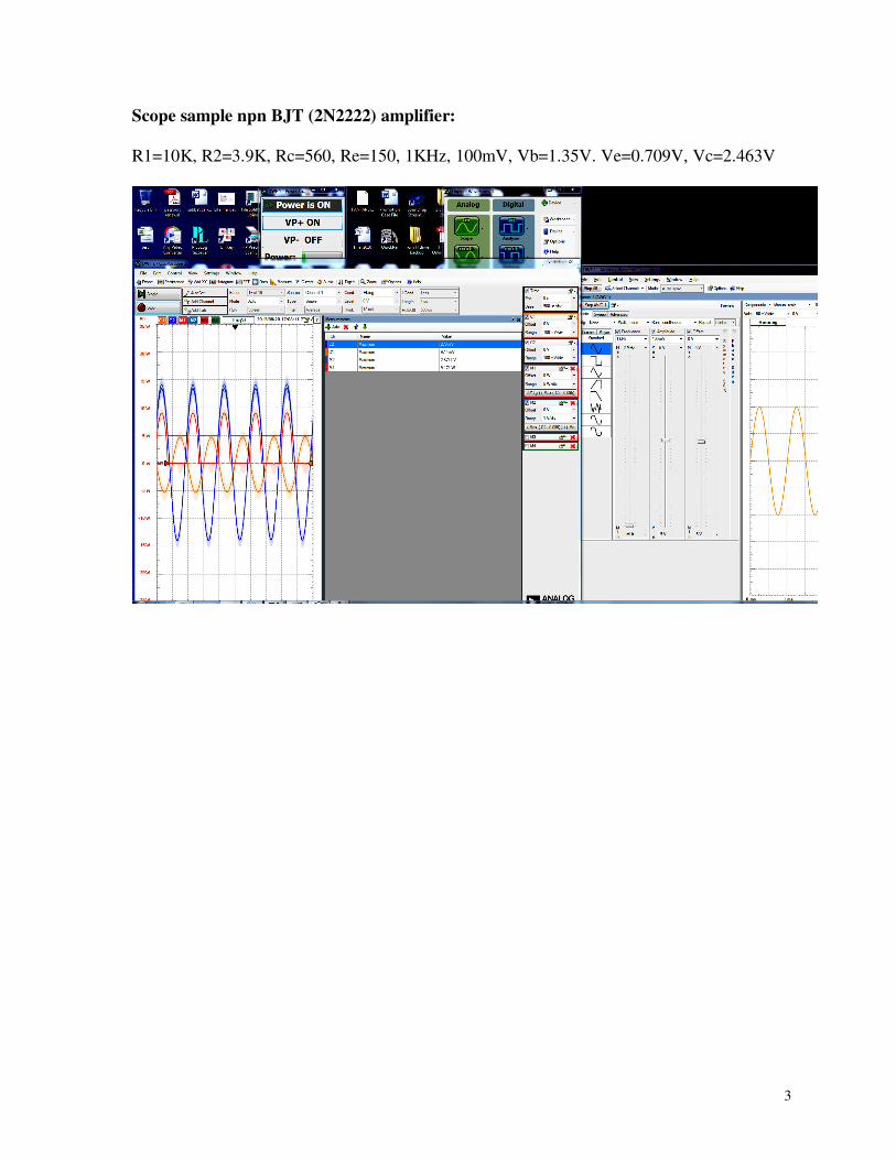
Figure 1: CE amplifier
C. Perform hand calculations for the output voltage and voltage gain. List the results from
your experiment, hand calculation as a table in your lab report.
D. Connect the load resistor RL = 1K to the amplifier. Read the output voltage from the
oscilloscope and find the voltage gain.
E. Connect a polarized capacitor CE =22uF to the circuit as shown in Figure 1 so that it is in
parallel with RE . At this time, the emitter is AC shorted to ground. Observe the output
waveform at Vc and Vo and copy it to your lab report. Explain why the waveforms are
distorted in your report. Once you have finished this step, recover the circuit connection
according to Figure 1 by removing CE and RL.
F. At the last step, you need to adjust the frequency of the input signal from the signal
generator. First you need to reduce the frequency and observe the voltage gain. The gain
will reduce after certain frequency. Find the frequency, fL, when the voltage gain
decreases to 70%. Then you need to increase the frequency and also find the input signal
frequency, fH, when voltage gain decreases to 70%. The amplifier bandwidth is defined as
fH-fL. Document the frequencies in your report.
G. Use “Sweep” function in the Arbitrary Waveform Generator to sweep the frequency of
the input signal and observe the response of the amplifier. Describe the response of the
amplifier.
H. Compare the results with the n-channel MOSFET amplifier in Lab 4.
I. Optional: Repeat the steps using 2N2907 (pnp) transistor. Comment on the differences
between npn and pnp amplifiers.
2N2222
+5V
To Channel 2 of
the oscilloscope RC
R2 RE
CC
CB
CE
To Channel 1 of the
oscilloscope
~ AWG1
R1 VC
VO VB
Vi RL
3
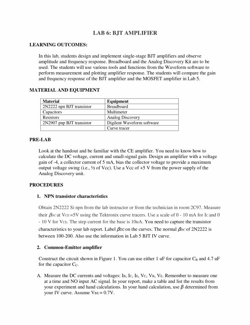
Scope sample npn BJT (2N2222) amplifier:
R1=10K, R2=3.9K, Rc=560, Re=150, 1KHz, 100mV, Vb=1.35V. Ve=0.709V, Vc=2.463V
4
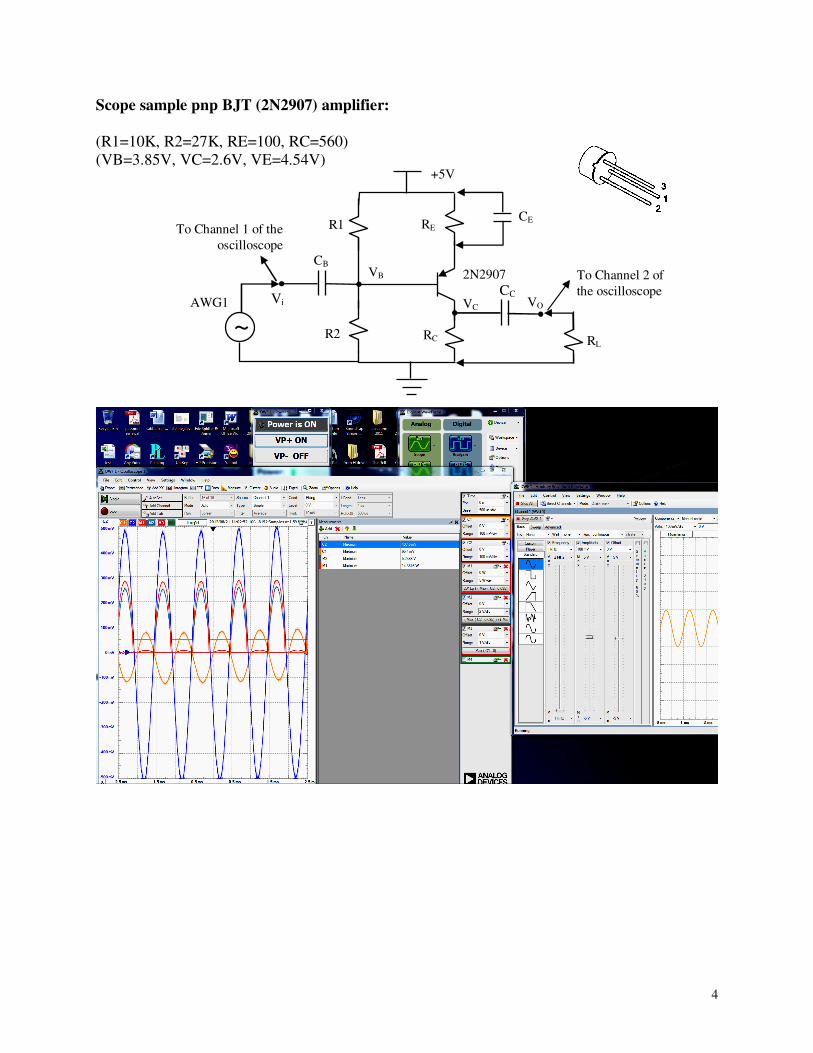
Scope sample pnp BJT (2N2907) amplifier:
(R1=10K, R2=27K, RE=100, RC=560)
(VB=3.85V, VC=2.6V, VE=4.54V)
2N2907
+5V
To Channel 2 of
the oscilloscope
RE
R2 RC
CC
CB
CE To Channel 1 of the
oscilloscope
~ AWG1
R1
VC VO
VB
Vi
RL
5
REFERENCES
1. Sedra/Smith, “Microelectronic Circuits,” 6th
Edition, Oxford University Press, 2010.
2. Mark N. Horenstein, “Instructor’s Resource Manual, Microelectronic Circuit and
Devices,” 2nd
Edition, Prentice Hall, 1996.
3. “A Complete Analog Design Kit for the Price of a Textbook,” Diligent,
http://www.digilentinc.com/Products/Detail.cfm?NavPath=2,842,1018&Prod=ANALOG
-DISCOVERY
4. n-channel MOSFET specification: http://www.vishay.com/docs/91127/sihfd110.pdf
5. p-channel MOSFET specification: http://www.micrel.com/_PDF/mic94050.pdf
6. n-channel MOSFET http://www.onsemi.com/pub_link/Collateral/BS107-D.PDF
7. 2N2222 npn BJT specification: http://www.onsemi.com/pub_link/Collateral/P2N2222A-
D.PDF
8. 2N2907 pnp BJT specification:
http://www.st.com/internet/com/TECHNICAL_RESOURCES/TECHNICAL_LITERAT
URE/DATASHEET/CD00003088.pdf