Embed Size (px)
Citation preview

Lab 3 Final report: Embedded Systems Digital Potentiometer
Subsystem
TEAM: RAR
EE 300W, Section 6 Professor Tim Wheeler
Rui Xia, Yuanpeng Liao and Ashwin Ramnarayanan
Table of Contents Introduction.......................................................................................................................2 Rationale...................................................................................................................... ...2 Implementation................................................................................................................3 Explanation of Code and Circuitry....................................................................................4 Verification Testing..........................................................................................................11 Validation Testing............................................................................................................19 Results from Integrated System ....................................................................................19 Discussion.......................................................................................................................20 Conclusion......................................................................................................................24 Appendices.....................................................................................................................24
1

Introduction As the complexity of today’s computer system grows, we can no long use a
single system to meet the requirement. At this time, we need to utilize embedded
system to break the main function into several subsystems. The purpose of this lab is to
integrate the four subsystems together and analyze the function of a black box. The four
subsystems contain digital-to-analog converter subsystem (D2A), digital potentiometer
subsystem (Digipot), analog to digital converter subsystem (A2D) and keypad
subsystem. D2A subsystem and Digipot subsystem will generate and input a waveform
into the black box. The output of the black box will be analyzed and sampled by the A2D
subsystem. Users can control the entire embedded system using the keypad
subsystem. By comparing the input and output of the black box, we can analyze the
behavior of the black box.
Our team is assigned to build the digital potentiometer subsystem. Digitpot
subsystem is used to scale the output of D2A subsystem and input the scaled waveform
into the black box. The output amplitude of the digital potentiometer subsystem is
selected by the keypad subsystem. It is crucial to generate a desired and consistent
input to the black box because we need to compare the input and output of the black
box.
Rationale Theory of Operation
In digital potentiometer subsystem, we need to scale the DAC subsystem output
(0-3.3V) to have a voltage range of 0 to +1, 2, 3, 4, or 5 V. Digital potentiometer is the
most important part in our subsystem because we need it to change the gain of the
amplifier and thus scale the input waveform. The digital potentiometer works as an
analog potentiometer. The wiper position Dn of the DigiPot selects the two resistors’
values RA and RB. 𝑅𝐴 = 𝑅𝐴𝐵 * (256 – 𝐷𝑛) / 256 and 𝑅𝐵 = (𝑅𝐴𝐵 * 𝐷𝑛) / 256. RA + RB =
RAB = 50kΩ for MCP41050 DigiPot. We choose to place RA between the input and
inverting terminal, and RB on the feedback path. Once we change the wiper position
2

based on the C++ code, the gain of the inverting amplifier will also change to our
desired value. In our C++ code, the subsystem outputs different scaled amplitudes
using 5 case statements.
Theory of Interfaces
Mebed is connected to PC to load C++ code to our circuit. We use SPI to
communicate the mbed to the DigiPot. The connections used were MOSI (Master-Out
Slave-In) and SCLK (clock). PuTTY can send and receive messages from the mebed
using USB port. CAN bus connects our subsystem and the keypad subsystem so that
the commands received from keypad subsystem will send to our subsystem.
Implementation
Circuitry:
Our subsystem should scale and map a 0 to 3.3V input from DAC to a 0 to 1V, 2V, 3V,
4V and 5V by selection. The selection of output range will be made via mbed according
to the can message from the keypad subsystem. An inverting amplifier circuit model
with a voltage divider is chosen.
3

Single-supply, programmable, inverting gain amplifier using a
digital potentiometer
Vin is the subsystem input and Vref is connected to ground. The gain equation is now
Vout = - Vin(Rwb/Rwa)
Variable gain Rwb / Rwa allows us to output a range no matter it is larger or smaller
than the input voltage. A second inverting amplifier with gain of 1 is added at Vout to
produce a positive output.
In experiment, we found that the resistors used in the second amplifier should be much
larger than the resistors in the first one to make an output waveform without any
clipping. We chose 2M ohm which is much larger than 50 k ohm (Rab). Also, a 10k ohm
resistor is added at Rb to stabilize the performance when Rwb is low.
4
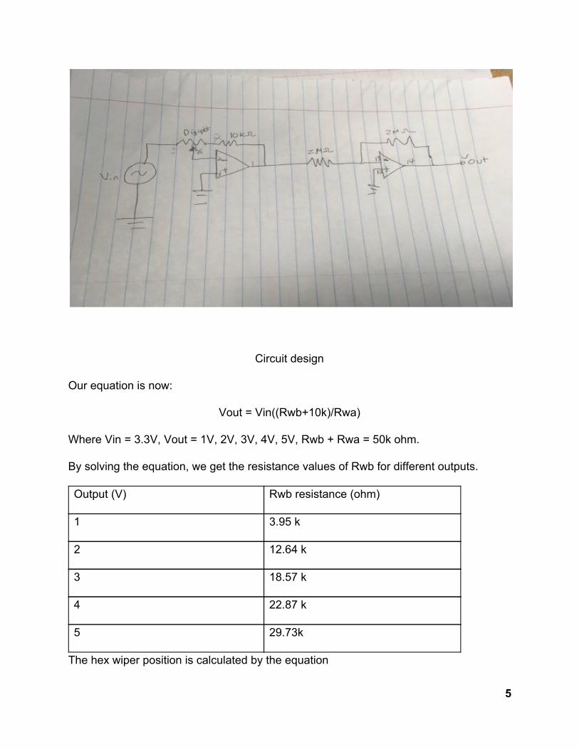
Circuit design
Our equation is now:
Vout = Vin((Rwb+10k)/Rwa)
Where Vin = 3.3V, Vout = 1V, 2V, 3V, 4V, 5V, Rwb + Rwa = 50k ohm.
By solving the equation, we get the resistance values of Rwb for different outputs.
Output (V) Rwb resistance (ohm)
1 3.95 k
2 12.64 k
3 18.57 k
4 22.87 k
5 29.73k
The hex wiper position is calculated by the equation
5

Dn = 256 * Rwb / Rab
where Rab = 50 k.
Adjustments are made to the calculated values based on experiments. The final wiper
positions are:
Output (V) Hex wiper position
1 0x14
2 0x21
3 0x31
4 0x33
5 0x46
Code:
An LPC 1768 mbed microcontroller will be coded with C language to realize the
following functions:
1. It gets the CAN-bus message from keypad subsystem via MCP 2551 CAN
transceiver to determine desired digital potentiometer output
2. It writes corresponding hex wiper position values to MCP 41050 digital potentiometer.
In the code, the can message will be read and stored by this line
CANMessage msg;
We used an if statement to test if there is any message received by the mbed and show
in LEDs:
if(can2.read(msg))
6
printf("Message received: %d\n", msg.data[0]);
led2 = !led2;
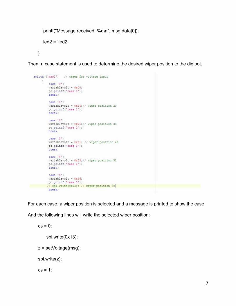
Then, a case statement is used to determine the desired wiper position to the digipot.
For each case, a wiper position is selected and a message is printed to show the case
And the following lines will write the selected wiper position:
cs = 0;
spi.write(0x13);
z = setVoltage(msg);
spi.write(z);
cs = 1;
7
cs=0 will select the chip first. The position 0x13 is the selected command bit. The
selected wiper position is written next. Finally, cs = 1 would deselect the chip.
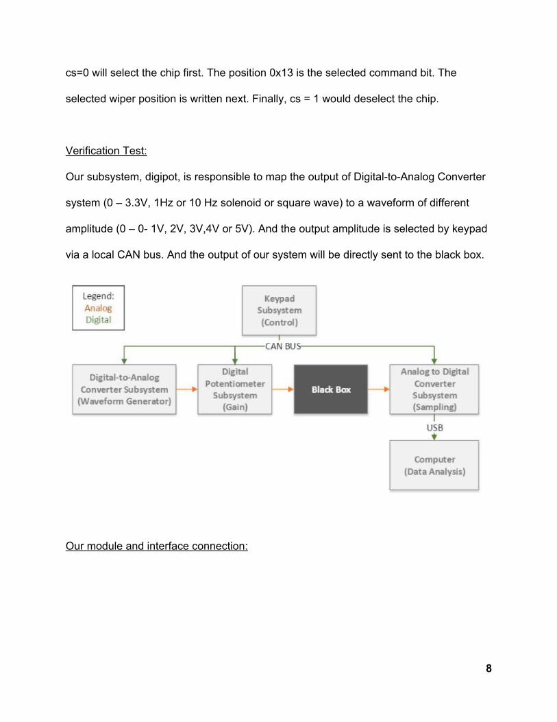
Verification Test:
Our subsystem, digipot, is responsible to map the output of Digital-to-Analog Converter
system (0 – 3.3V, 1Hz or 10 Hz solenoid or square wave) to a waveform of different
amplitude (0 – 0- 1V, 2V, 3V,4V or 5V). And the output amplitude is selected by keypad
via a local CAN bus. And the output of our system will be directly sent to the black box.
Our module and interface connection:
8
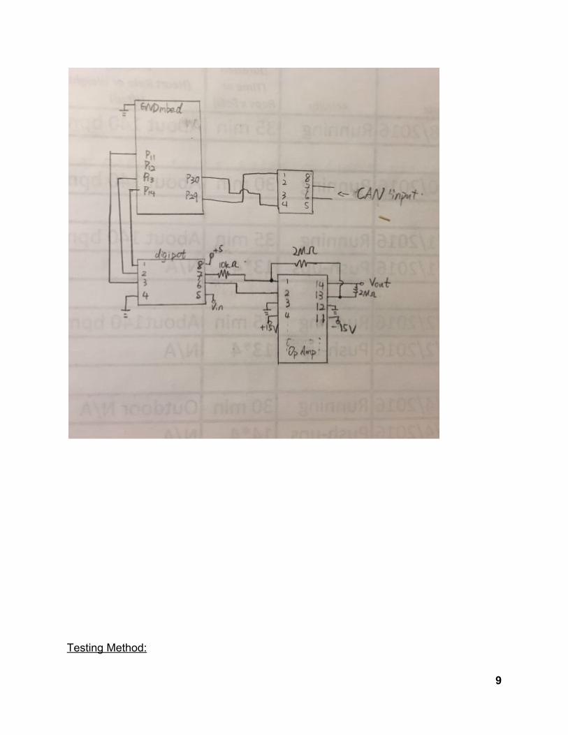
Testing Method:
9
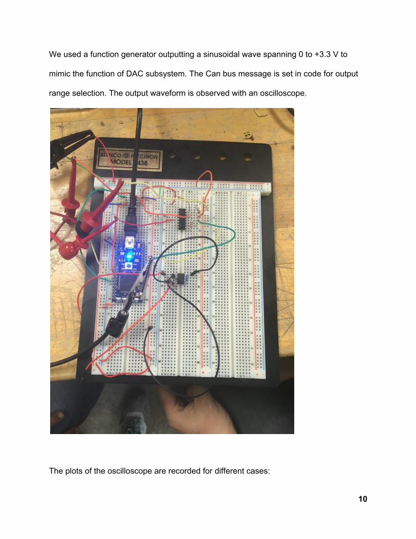
We used a function generator outputting a sinusoidal wave spanning 0 to +3.3 V to
mimic the function of DAC subsystem. The Can bus message is set in code for output
range selection. The output waveform is observed with an oscilloscope.
The plots of the oscilloscope are recorded for different cases:
10

1V:
2V:
11
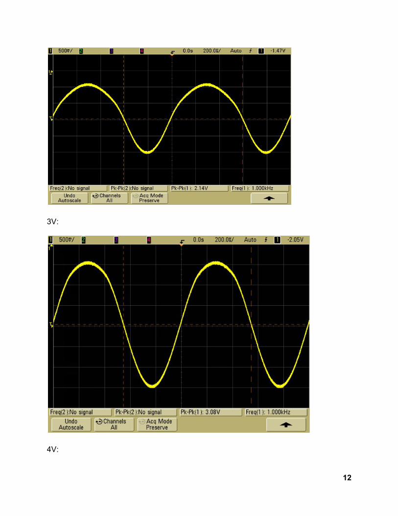
3V:
4V:
12
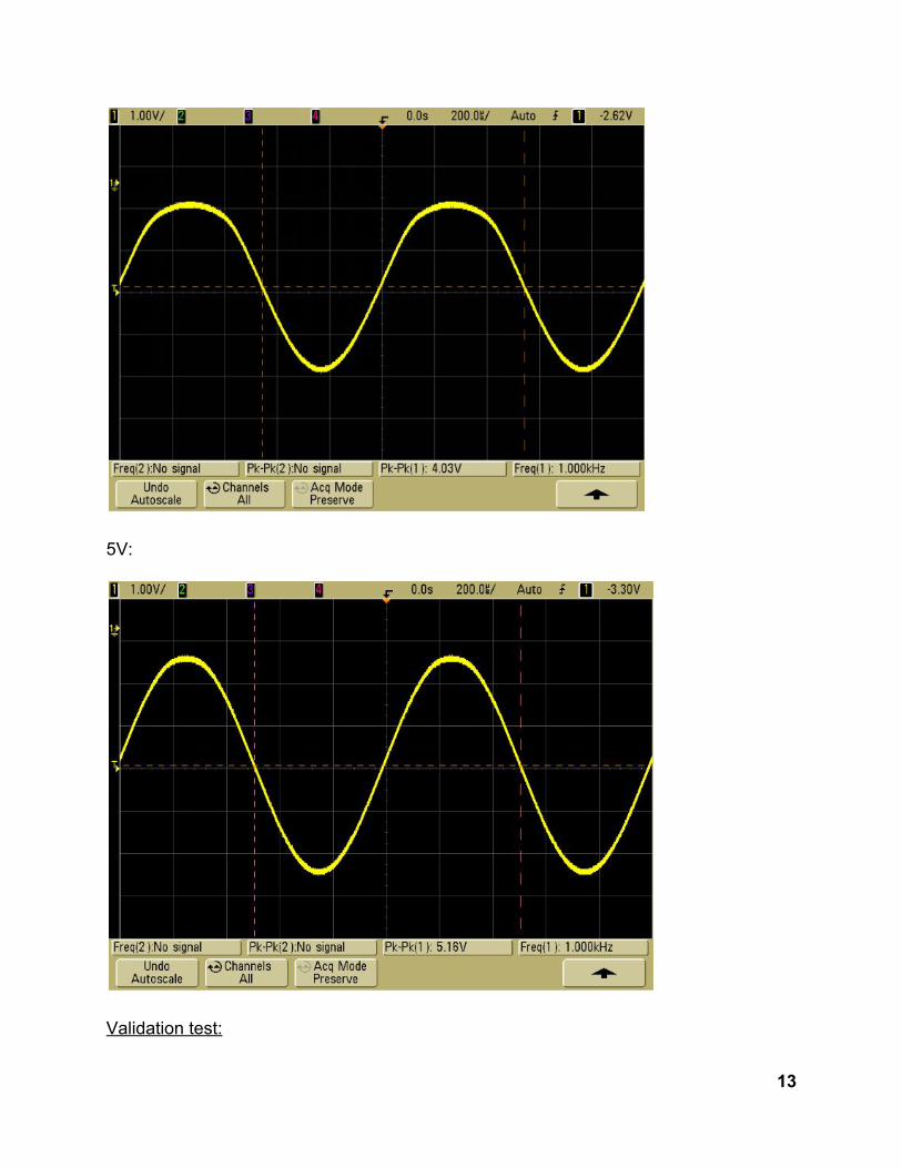
5V:
Validation test:
13
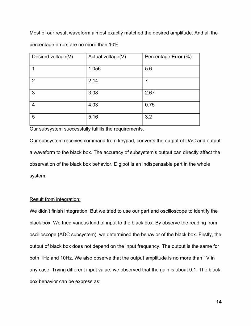
Most of our result waveform almost exactly matched the desired amplitude. And all the
percentage errors are no more than 10%
Desired voltage(V) Actual voltage(V) Percentage Error (%)
1 1.056 5.6
2 2.14 7
3 3.08 2.67
4 4.03 0.75
5 5.16 3.2
Our subsystem successfully fulfills the requirements.
Our subsystem receives command from keypad, converts the output of DAC and output
a waveform to the black box. The accuracy of subsystem’s output can directly affect the
observation of the black box behavior. Digipot is an indispensable part in the whole
system.
Result from integration:
We didn’t finish integration, But we tried to use our part and oscilloscope to identify the
black box. We tried various kind of input to the black box. By observe the reading from
oscilloscope (ADC subsystem), we determined the behavior of the black box. Firstly, the
output of black box does not depend on the input frequency. The output is the same for
both 1Hz and 10Hz. We also observe that the output amplitude is no more than 1V in
any case. Trying different input value, we observed that the gain is about 0.1. The black
box behavior can be express as:
14
Vout = 1V- 0.1 Vin
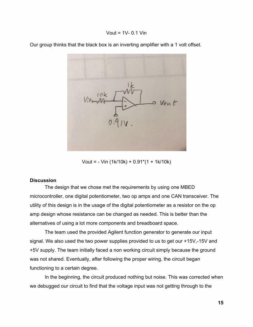
Our group thinks that the black box is an inverting amplifier with a 1 volt offset.
Vout = - Vin (1k/10k) + 0.91*(1 + 1k/10k)
Discussion
The design that we chose met the requirements by using one MBED
microcontroller, one digital potentiometer, two op amps and one CAN transceiver. The
utility of this design is in the usage of the digital potentiometer as a resistor on the op
amp design whose resistance can be changed as needed. This is better than the
alternatives of using a lot more components and breadboard space.
The team used the provided Agilent function generator to generate our input
signal. We also used the two power supplies provided to us to get our +15V,-15V and
+5V supply. The team initially faced a non working circuit simply because the ground
was not shared. Eventually, after following the proper wiring, the circuit began
functioning to a certain degree.
In the beginning, the circuit produced nothing but noise. This was corrected when
we debugged our circuit to find that the voltage input was not getting through to the
15

MBED. After rewiring, we obtained a periodic function and resembled a wave. This was
due to incorrect resistor values as we found out later on. After, the values were
changed, the code had to be changed in the case structures for the HEX values. Finally,
after the final debugging we were able to obtain our sine wave.
This entire process took up the entirety of our time. Thus, the team was unable to
work with the other teams for a significant amount of time. The teams were unable to
link the CAN buses together to get a common voltage signal through them and control
the black box using the keypad. This is the result of time management and
communication issues both within and outside the team. This would be the main area of
improvement for the group moving forward.
Finally, the teams tried identifying what was in the black box. We were
successfully able to get the 1 Volt offset answer correct but were unable to calculate the
slope. The final waveform function was:
Y = -0.1X + 1 V
Future areas of improvement would involve proper communication amongst the
team members in order to manage time efficiently. A lot of work was required to be
done outside the given lab period of time which was not used properly.
Value Statement: In this lab, we are required to communicate with other groups to accomplish an integrated project. This is the first time we encounter this setting. However, we can certainly imagine that this kind of scenario is far from rarely happen in an engineer’s career. We were a little confused at the beginning. This resulted in the failure that we could not finish the integration. This experience greatly enhances our communication skill and prepares us for the inevitable. Technically, this is also the first time for most of us to use LCP 1768 mbed and an online compiler. Being able to work with various languages and compilers is a great contributor to a successful career. This lab shows us a continuously learning process example and gives us some experience about it.
16
Conclusion
Team RAR successfully completed the DigiPot subsystem that received the input signal and could control the resistor values in 5 different cases. The teams were unsuccessful in integrating the subsystems together whose entire purpose was to divide the work instead of loading all of it on one program. The utility of this project goes into security and control systems. The CAN buses enables us to integrate multiple subsystems into one giant process. This allows for continuous improvement to a given process and simultaneously makes debugging much easier for the engineers. Appendixes
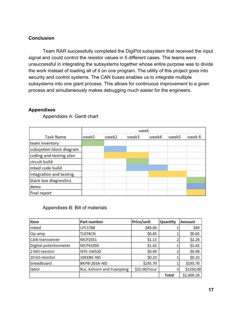
Appendixes A: Gantt chart
Appendixes B: Bill of materials
17
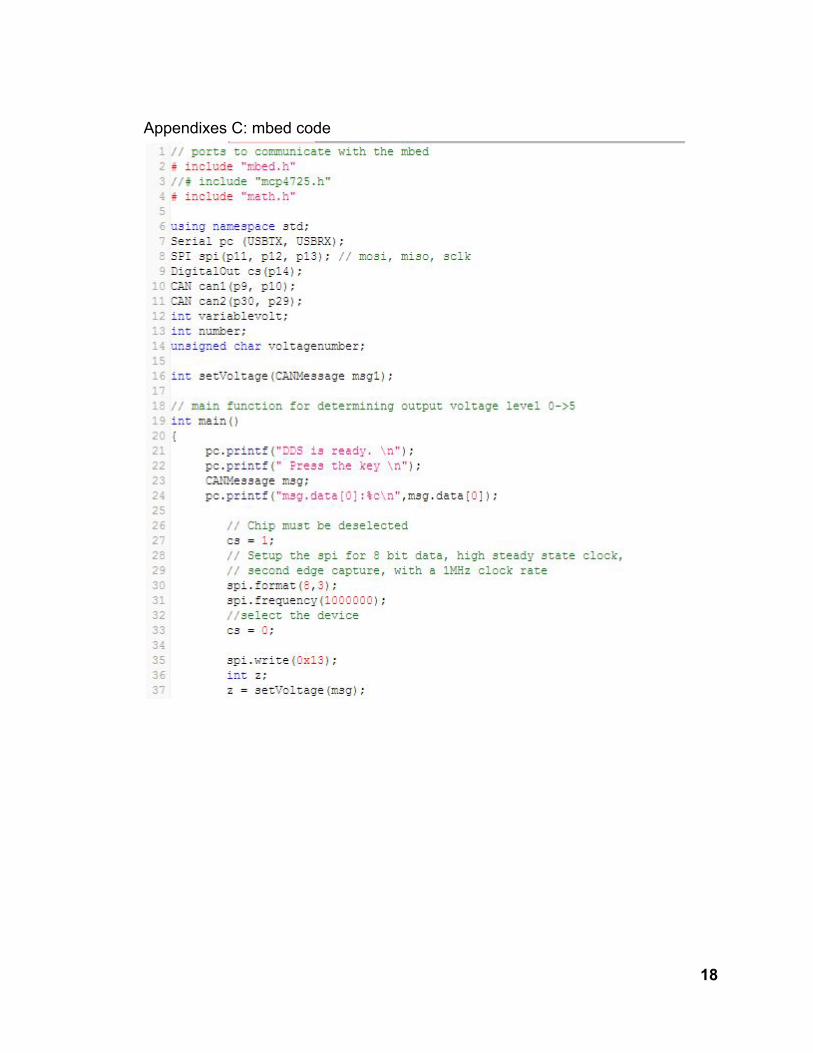
Appendixes C: mbed code
18

19
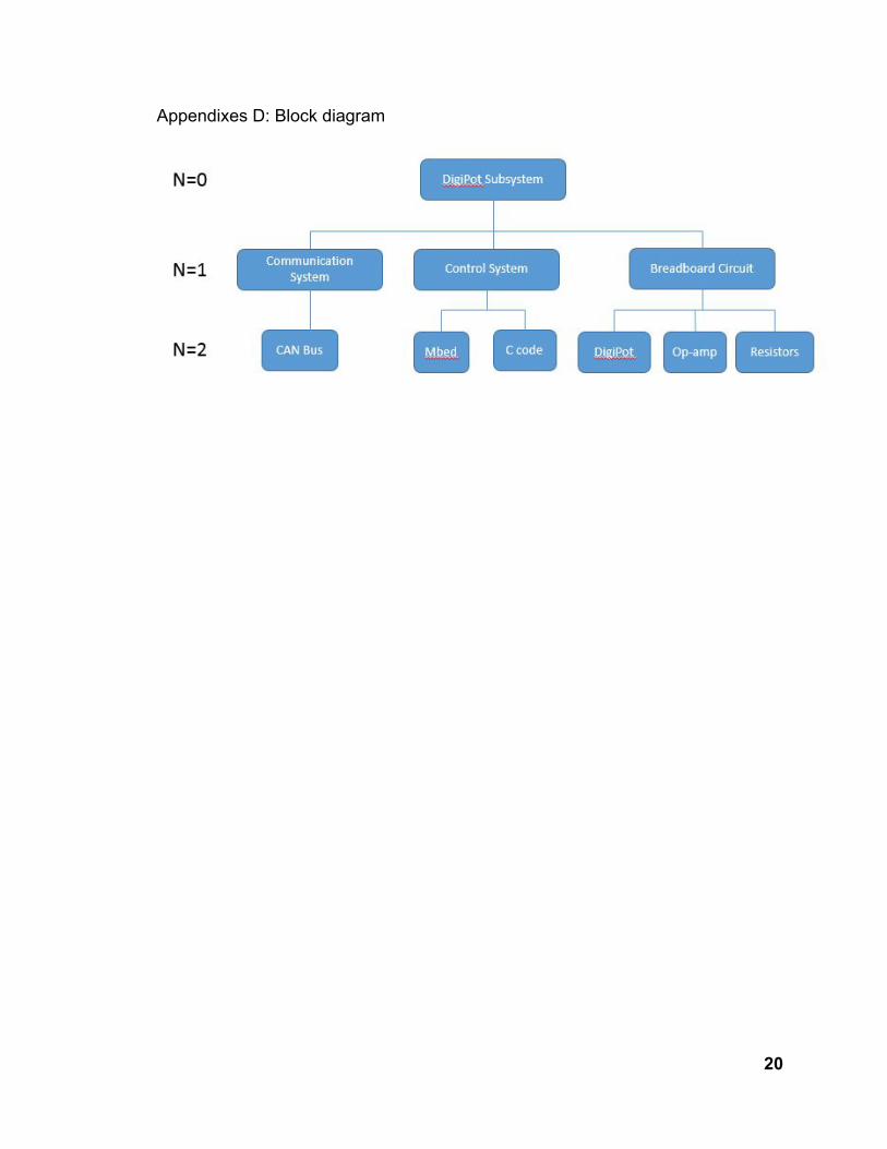
Appendixes D: Block diagram
20