Embed Size (px)
Citation preview

KL-620 Microcomputer Sensing Control System
Training Course

Main Unit
Unit 0 : KL-62001
GeneralSensors (I)
Unit 1 : KL-64001
GeneralSensors (II)
Unit 2 : KL-64002
PressureStrain Gauge
Unit 7 : KL-64007
F/V Converter
Unit 11 : KL-64011
CDSPhotovoltaic
Unit 9 : KL-64009
V/F Converter
Unit 10 : KL-64010
Temp II (PT100)
Unit 12 : KL-64012
Fiber Optic
Unit 14 : KL-64014
Hall CurrentProximity
Unit 8 : KL-64008
LVDT
Unit 15 : KL-64015
Gas/SmokeEthanol
Unit 4 : KL-64004
Rotation Angle
Unit 16 : KL-64016
Level (Water)
Unit 13 : KL-64013
InfraredUltrasonic
Unit 6 : KL-64006
GeneralSensors (III)
Unit 3 : KL-64003
Temp I (AD590)Humidity
Unit 5 : KL-64005

Main Unit
Unit 0 : KL-62001
In this Unit, the operation of each block on Main Unit will be introduced. After study complete, users are able to use KL-62001 as measurement and assist tool for KL-620 experiments.
Menu
1. System Test
2. DCV Measurement (Manual)
3. DCV Measurement (Chip)
4. DCV Measurement (PC)
5. D/A Converter Test
6. Alarm Amplifier Test
7. Comparator Test
8. Differential Amplifier Test
9. Instrumentation Amplifier
10. Other MCU Function Test

System Test
Single ChipOut Control 2Out Control 3
Status Display
Thumbwheel Switch
EPROM
Blocks to be demonstrated:Blocks to be demonstrated:
Objective:Objective:To understand how to self test Single Chip and EPROM.
Back
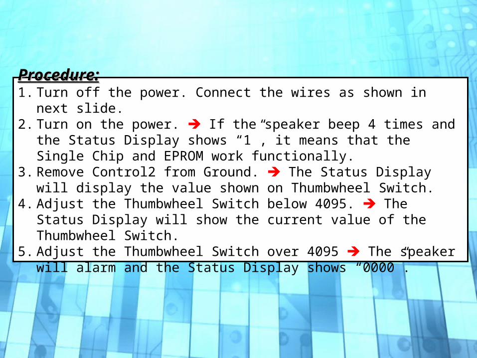
Procedure:Procedure:1. Turn off the power. Connect the wires as shown in next slide.2. Turn on the power. If the speaker beep 4 times and the Status
Display shows “1”, it means that the Single Chip and EPROM work functionally.
3. Remove Control2 from Ground. The Status Display will display the value shown on Thumbwheel Switch.
4. Adjust the Thumbwheel Switch below 4095. The Status Display will show the current value of the Thumbwheel Switch.
5. Adjust the Thumbwheel Switch over 4095 The speaker will alarm and the Status Display shows “0000”.

Control3 GND
Control2 GND

DCV Measurement (Manual)
Objective:Objective:To understand how to use Potentiometer.To use DC Voltage Meter to measure DC Voltage manually.
DC Power+12V, -12V
Select / Manual
Status DisplayMODE ButtonRange Button
Blocks to be demonstrated:Blocks to be demonstrated:
Potentiometer
Back

Procedure:Procedure:1. Turn off the power. 2. Connect the wires as shown in next slide.3. Turn on the power. 4. Press Range button twice. Select the measuring range of DCV ( -20V
~ +20V)5. Rotate the Potentiometer. The output voltage at VR2 will display at
Status Display section (-12V ~ +12V) .
Discussion:Discussion:
When connects MANUAL to the GND, Status Display Section acts as DC Voltage Meter.

+Input VR2
-12V VR1
Manual GND
+12V VR3
Connect to GND

DCV Measurement (Chip)
Objective:Objective:Use A/D Converter, Single Chip and Status Display to measure DC voltage
DC Power+5V, GND
Select / Chip
Status DisplayMODE ButtonRange Button
Blocks to be demonstrated:Blocks to be demonstrated:
Potentiometer
A/D Converter
Back

Procedure:Procedure:1. Turn off the power. 2. Connect the wires as shown in next slide. 3. Turn on the power. 4. Press Range button twice. Select the measuring range of DCV ( -20V
~ +20V)5. Rotate the Potentiometer. The output voltage at VR2 will display at
Status Display section (0V ~ +5V) .
Discussion:Discussion:
1. When connecting CHIP to the GND, the analog signal received from A/D Converter will send to single chip for decoding and output to 7 segment display.
2. When sending the analog signal to the PC, the signal should be converted to digital format. As the result, this technique will be used when connecting the main unit to the PC. Check next exercise.
Warning!!The max voltage input to ADC is 5V.

A/D IN VR2
+5V VR1
GND VR1
Chip GND
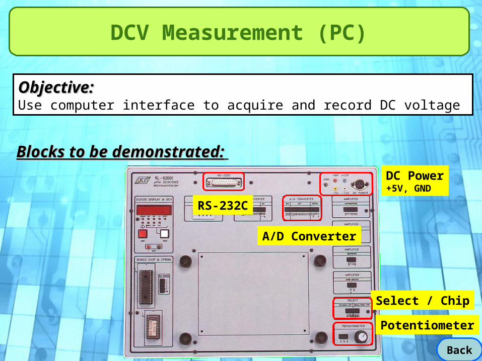
DCV Measurement (PC)
Objective:Objective:Use computer interface to acquire and record DC voltage
DC Power+5V, GND
Select / Chip
RS-232C
Blocks to be demonstrated:Blocks to be demonstrated:
Potentiometer
A/D Converter
Back

Procedure:Procedure:1. Turn off the power and connect the wires as shown in next slide. 2. Connects RS-232C port to PC COM port by using K&H RS-232 Cable. 3. Turn on the power and launch the KL-620 software. 4. Press the [Acquire] button. Start to record the DC voltage. 5. Rotate the Potentiometer. The output voltage at VR2 will display at
software panel.
Discussion:Discussion:When connecting CHIP to the GND and CTRL pin to GND, the analog signal received from A/D Converter will send to PC through RS-232 interface.
Warning!!The max voltage swing input to ADC is -5V ~ +5V.

A/D IN VR2
+5V VR3
GND VR1
Chip GND
CTRL GND
Connect to PC COM1

Press acquire button to start acquire data
Save data in Excel format
Load saved data
Setup Acquire Frequency, Number and Gain
Change Y-axis Name and Scale
Graphic and Cursor control panel
Data stored in Table
Current, Min, and Max value
Setup trigger level for background color
KL-620 Software Interface for Data Acquisition

D/A Converter Test
Objective:Objective:Use DCV to measure the voltage converted from D/A Converter
Select / Manual
Blocks to be demonstrated:Blocks to be demonstrated:
D/A Converter
Thumbwheel Switch
Status Display
Back

Procedure:Procedure:1. Turn off the power and connect the wires as shown in next slide. 2. Turn on the power.3. Press Range button twice Setup DCV measuring range (-20V ~ +20V)4. Adjust Thumbwheel Switch below 4095, for example 3512 Status
Display will show close to 3.512, meaning that the output voltage of DA Converter is 3.512 Volt.
5. Adjust Thumbwheel Switch above 4095 Status Display will show close to 0.000 and speaker start beeping.
Discussion:Discussion:
The digital output of thumbwheel switch (12-bit) is connected to 12-bit D/A Converter DA0~DA11 and convert to DC voltage.
The scale for converting is 1 bit = 0.001Vi.e. (0000~4095 => 0.000~4.095V)

+Input OUT+
Manual GND
Connect to GND
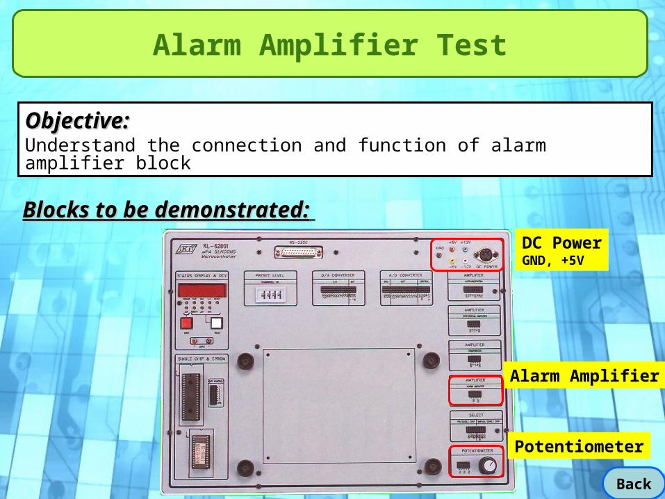
Alarm Amplifier Test
Objective:Objective:Understand the connection and function of alarm amplifier block
Alarm Amplifier
Blocks to be demonstrated:Blocks to be demonstrated:
DC PowerGND, +5V
Potentiometer
Back

Procedure:Procedure:1. Turn off the power and connect the wires as shown in next slide. 2. Turn on the power.3. Rotate the Potentiometer When the applied voltage is higher than
0.7V, the buzzer will be ON.
Discussion:Discussion:
The schematic of the Alarm Amplifier block is shown below. When the applying voltage to Signal Input of Alarm Amplifier is above around 0.7 volt, transistor will be ON and the buzzer will start alarming.
Signal Input
From Single Chip
Buzzer

+5V VR3
GND VR1 SIN. IN VR2

Comparator Test
Objective:Objective:Understand the connection and function of comparator block
Comparator
Blocks to be demonstrated:Blocks to be demonstrated:
DC PowerGND, +5V,+12V
Potentiometer
Select / Manual
Back
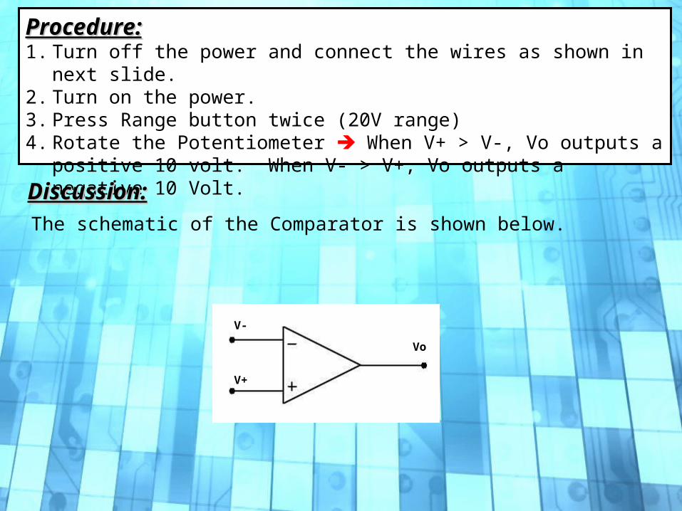
Procedure:Procedure:1. Turn off the power and connect the wires as shown in next slide. 2. Turn on the power.3. Press Range button twice (20V range)4. Rotate the Potentiometer When V+ > V-, Vo outputs a positive 10
volt. When V- > V+, Vo outputs a negative 10 Volt.
Discussion:Discussion:The schematic of the Comparator is shown below.
V-
Vo
V+

+12V VR3
GND VR1
+5V V-
V+ VR2
+Input Vo
Manual GND
Connect to GND

Differential Amplifier Test
Objective:Objective:Understand the connection and function of differential amplifier block.
Differential Amplifier
Blocks to be demonstrated:Blocks to be demonstrated:
DC Power+12V, +5V,-5V
Select / Manual
Back

Procedure:Procedure:1. Turn off the power and connect the wires as shown in next slide. 2. Turn on the power. 3. Select Range button to 20V range The Status Display shows 7 (Volt). 4. Connects V+ to DC -5V and V- remains connecting to DC +5V The
Status Display shows -10 (Volt)
The output voltage of differential amplifier is equal to V+ - V-. However due to the power supplied limit of amplifier, the maximum difference is equal to 12 Volt. The schematic of the differential amplifier is shown and explained below.
V-
Vo
V+
10k
10k
10k10k
V+
2
I
I
Discussion:Discussion:

+5V V-
Manual GND
+12V V+
+Input Vo
Connect to GND

Instrumentation Amplifier Test
Objective:Objective:Understand the connection and function of instrumentation amplifier block.
InstrumentationAmplifier
Blocks to be demonstrated:Blocks to be demonstrated:
Potentiometer
Select / Manual
D/A Converter
Thumbwheel Switch
Back

Procedure:Procedure:1. Turn off the power. 2. Use multi-meter and adjust Potentiometer until the resistance between
VR2 and VR3 is equal to 40k Ohm.3. Setup Thumbwheel Switch to be 0200 D/A Converter OUT+ = 0.2 Volt4. Connect wires as shown in next page.5. Turn on the power.6. Select Range button to 20V range Status Display shows 1.2V
VoVR
R1:100k
R1:100k
R2:10k
R2:10k
R3:10k
R3:10k
VR1
VR3
VR2
Vi-
Vi+Discussion:Discussion:
The schematic of the instrumentation amplifier block is shown at right side, where
= 6

VR3 VR3
OUT+ V-
GND V+
Manual GND
VR2 VR2
VR1 VR1
+Input Vo
Connect to GND

Other MCU Function Test
Single ChipOut Control 1Out Control 4
Status Display
Thumbwheel Switch
Blocks to be demonstrated:Blocks to be demonstrated:
Objective:Objective:To understand the Out Control pin1 and pin4 of MCU block
Alarm Amplifier
A/D Converter
DC Power+5V, GND
Potentiometer
Select / Chip
Back

Procedure:Procedure:1. Turn off the power. Connect the wires as shown in next slide.2. Setup Thumbwheel Switch to be [1000] Setup Alarm level equal to
1.221 Volt. (See discussion below)3. Turn on the power. 4. Select Range button to 20V range5. Adjust the Potentiometer so that the Status Display shows higher than
1.221 (Volt) Out Control 1 outputs a continuous pulse (pulse width = 0.5 sec) to the alarm amplifier and enable the alarm.
6. Adjust the Potentiometer so that the Status Display shows lower than or equal to 1.221 (Volt) Out Control 1 outputs a LOW state, no sound outputs from alarm.
7. Remove Out Control 1 from Alarm Amplifier SIN. IN 8. Connect Out Control 4 to Alarm Amplifier SIN. IN9. Adjust the Potentiometer so that the Status Display shows higher than
1.221 (Volt) Out Control 4 outputs a LOW state. 10.Adjust the Potentiometer so that the Status Display shows lower than or
equal to 1.221 (Volt) Out Control 4 outputs a HIGH state and alarm amplifier starts alarming.
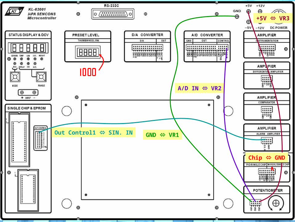
A/D IN VR2
+5V VR3
GND VR1
Chip GND
Out Control1 SIN. IN
Discussion:Discussion:
0000
1221
2442
3663
4884
5000
0
1000
2000
3000
4000
4095
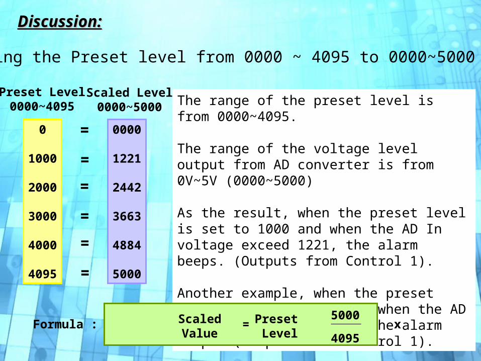
Preset Level0000~4095
=
Scaling the Preset level from 0000 ~ 4095 to 0000~5000
The range of the preset level is from 0000~4095.
The range of the voltage level output from AD converter is from 0V~5V (0000~5000)
As the result, when the preset level is set to 1000 and when the AD In voltage exceed 1221, the alarm beeps. (Outputs from Control 1).
Another example, when the preset level is set to 3000 and when the AD In voltage exceed 3663, the alarm beeps. (Outputs from Control 1).
Scaled Level0000~5000
Formula : = x5000
4095
ScaledValue
Preset Level
=
=
=
=
=

General Sensors (I)
You have learned how to use Main Unit KL-62001 as a measurement and assist tool from previous Unit. In this Unit, 4 different types of common sensors are introduced. The connections of the modules to the Main Unit will not be introduced. Any questions regard to the Main Unit connections can be referred to Unit 0.
Menu
1. Photo Transistor
2. Photo Interrupter
3. Magnetic Hall Effect (Digital)
4. Magnetic Hall Effect (Analog)
Unit 1 : KL-64001

Photo Transistor
Back
Structure:Structure: Symbol:Symbol:
Wire
Chip
Window
Lead wire
C
E
The electrons that are generated by photons in the base-collector junction are injected into the base, and this current is then amplified by the transistor operation. i.e., The light striking the base replaces what would ordinarily be voltage applied to the base – so, a phototransistor amplifies variations in the light striking it.

Circuit Explanation:Circuit Explanation:
Ic
Iλ
photons
Photons Iλ Ic Vo1WHEN
Photons Iλ Ic Vo1WHEN

Experiment Procedure:Experiment Procedure:• With power off, connect Vo1 to the Main Unit DCV INPUT+.• Turn on the power.• Cover the phototransistor with hand and record the output voltage Vo1?
• Lighten the phototransistor with fluorescent lamp and record the output
voltage Vo1? • What is the relation between the output voltage and the distance
between light source and phototransistor?
Answers:Answers:3. ~ 5 Volt4. 0.1 V ~ 4.0 V, depends on the magnitude of the light source. 5. The longer the distance, the higher output voltage
Note: If you don’t know how to use DCV, please check Unit 0

Photo Interrupter
Back
Structure:Structure: Symbol:Symbol:
DetectorEmitter
Barrier
Lead wireFixed hole
D
++
E
A common implementation involves an LED and a Phototransistor, separated so that light may travel across a barrier but electrical current may not. When an electrical signal is applied to the input of the photo interrupter, its LED lights, its light sensor then activates, and a corresponding electrical signal is generated at the output.

Circuit Explanation:Circuit Explanation:
Vo2’
Ic
In normal situation:Detector receives light signal from LED Vo2’ = LOW Vo2 = LOW
When an object block the light bean:Collector current Ic decreases Vo2’ = High Vo2 = High
The two inverters act as a wave shaper and Schmitt trigger Latch.

Experiment Procedure:Experiment Procedure:1. With power off, connect Vo2 to the SIN. IN of Alarm Amplifier of on
Main Unit.2. Turn on the power.3. What’s the status of the alarm when nothing block the light bean?4. What’s the status of the alarm when an object blocks the light bean? 5. Use oscilloscope to compare the wave shape of Vo2’ and Vo2
Note: If you don’t know how to use DCV, please check Unit 0
Answers:Answers:3. nothing happened4. start alarming 5.
Vo2
Vo2’
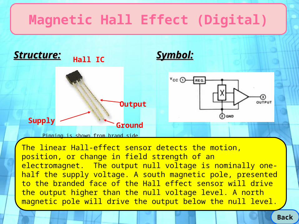
Magnetic Hall Effect (Digital)
Back
Structure:Structure: Symbol:Symbol:
Output
SupplyGround
The linear Hall-effect sensor detects the motion, position, or change in field strength of an electromagnet. The output null voltage is nominally one-half the supply voltage. A south magnetic pole, presented to the branded face of the Hall effect sensor will drive the output higher than the null voltage level. A north magnetic pole will drive the output below the null level.
Pinning is shown from brand side
Hall IC

Circuit Explanation:Circuit Explanation:
The voltage of Vo3’ is affected by the pole and magnitude of the magnetic field.
When South pole approaches to the sensor Vo3’
When North pole approaches to the sensor Vo3’
The two inverters act as a wave shaper and Schmitt trigger Latch.
Vo3’
Magnet
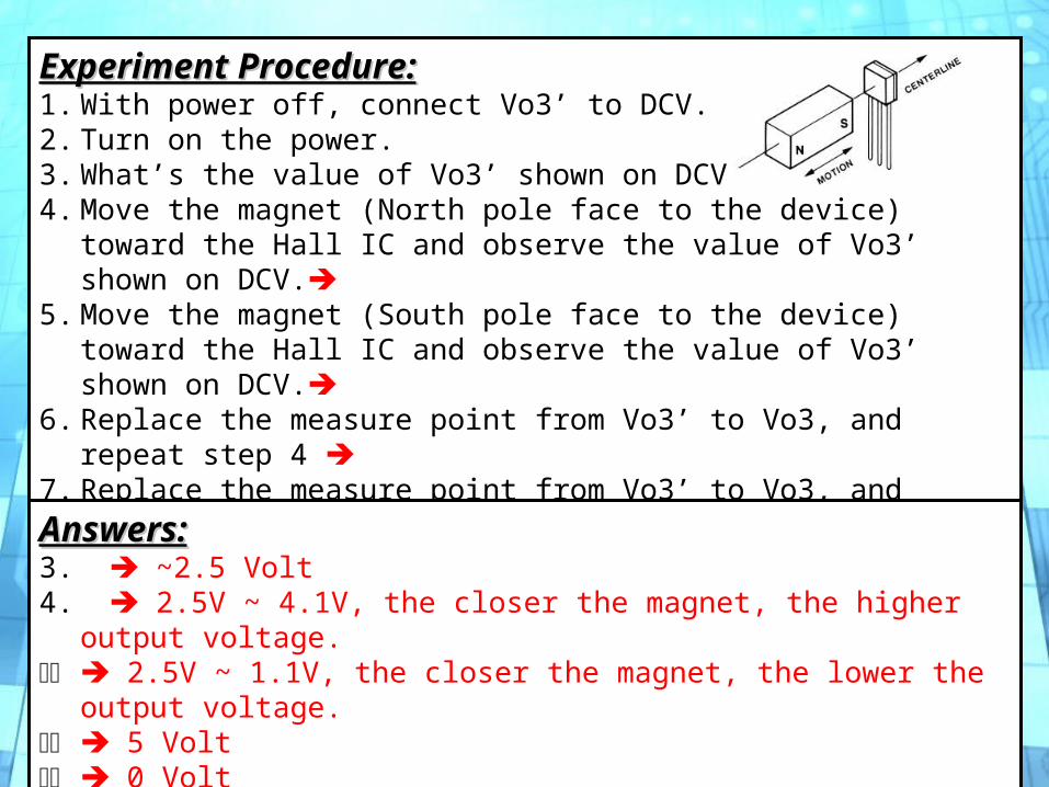
Experiment Procedure:Experiment Procedure:1. With power off, connect Vo3’ to DCV.2. Turn on the power.3. What’s the value of Vo3’ shown on DCV? 4. Move the magnet (North pole face to the device) toward the Hall IC and
observe the value of Vo3’ shown on DCV.5. Move the magnet (South pole face to the device) toward the Hall IC and
observe the value of Vo3’ shown on DCV.6. Replace the measure point from Vo3’ to Vo3, and repeat step 4 7. Replace the measure point from Vo3’ to Vo3, and repeat step 5
Answers:Answers:3. ~2.5 Volt4. 2.5V ~ 4.1V, the closer the magnet, the higher output voltage.55 2.5V ~ 1.1V, the closer the magnet, the lower the output voltage.55 5 Volt55 0 Volt

Magnetic Hall Effect (Analog)
Back
Structure:Structure: Symbol:Symbol:
The Hall element provides an output voltage that is proportional to the magnetic filed which it is exposed. The sensed magnetic field can be either positive or negative. As a result, the output of the amplifier will be driven either positive or negative
GND
Vout1Vin
Vin
GND
Vout1 Vout2
Vout2
Hall Element

Circuit Explanation:Circuit Explanation:
The voltage of Vout1 and Vout2 is affected by the pole and magnitude of the magnetic field.
When South pole approaches to the sensor Vout1 Vout2 Vo4
When North pole approaches to the sensor Vout1 Vout2 Vo4
Variable resistor R9 is used for offset adjustment.
Magnet
Vout1 Vout2

Experiment Procedure:Experiment Procedure:1. With power off, connect Vo4 to DCV.2. Turn on the power.3. Adjust variable resistor R9 so that Vo4 is equal to 0 Volt. 4. Move the magnet (North pole face to the device) toward the Hall IC and
observe the value of Vo4 shown on DCV.5. Move the magnet (South pole face to the device) toward the Hall IC and
observe the value of Vo4 shown on DCV.
Answers:Answers:4. Vo4 = 0 ~ 6 Volt The closer the magnet, the higher output voltage (positive direction).5. Vo4 = 0 ~ -6 Volt The closer the magnet, the higher output voltage (negative direction).
General Sensors (II)
Menu
5. Pyroelectric Detector
6. Reed Switch
7. Thermistor
8. Mercury Switch
Unit 2 : KL-64002

Pyroelectric Detector
Back
Structure:Structure: Symbol:Symbol:
The pyroelectric sensor is made of a crystalline material that generates a surface electric charge when exposed to heat in the form of infrared radiation. When the amount of radiation striking the crystal changes, the amount of charge also changes and can then be measured with a sensitive FET device built into the sensor. The sensor elements are sensitive to radiation over a wide range so a filter window is added to the package to limit incoming radiation to the 8 to 14μm range which is most sensitive to human body radiation.
Filter Window
DrainSource Gate
D
SG

Circuit Explanation:Circuit Explanation:
When human body towards to the sensor a negative pulse signal should present at the source terminal of FET U1 amplifies the pulse
When human body away from the sensor a positive pulse signal should present at the source terminal of FET U1 amplifies the pulse
Coupling Capacitor C1 blocks the DC signal from the sensor.
Vs

Experiment Procedure:Experiment Procedure:1. With power off, connect CH1 of the oscilloscope to Vo5.2. Set oscilloscope CH1 to AC coupling (500mV,500mS)3. Adjust variable resistor R5 to maximum (rotate the knob clockwise until
reaching end position)4. Turn on the power.5. Weave your hand on the top of the sensor and observe the waveform
shown on the oscilloscope 6. Toward your hand to the top of the sensor slowly, stay for 2 sec, and
remove your hand away from the sensor slowly, check the waveform
Answers:Answers:
5. 6.
Toward
Away
Toward
Away

Reed Switch
Structure:Structure: Symbol:Symbol:
The reed switch is a type of mechanical-contact switch. Two metal reeds are enclosed in a hermetically sealed glass capsule. A normally open (NO) reed switch is shown above. The overlapping reeds can be closed or opened by positioning a permanent magnet close to the reed contacts.
Reed
Contact
Sealed glass
Back

Circuit Explanation:Circuit Explanation:
When switch close Q1 ON Buzzing
When switch open Q1 OFF No Buzzer

Experiment Procedure:Experiment Procedure:1. Power On the module.2. Approach a magnet from the top of the sensor to the sensor contact
(Magnetic field is in vertical with the contact plate). What is the status of the buzzer?
3. Approach a magnet from the side of the sensor to the sensor contact.(Magnetic field is in parallel with the contact plate). What is the status of the buzzer?
Answers:Answers: 2. Buzzer is ON3. Buzzer is OFF

Thermistor
Structure:Structure: Symbol:Symbol:
Thermistors are temperature sensitive resistors. Increasing the temperature will decreases the resistance (in most cases). This type also called NTC type (Negative Temperature Coefficient). When used for temperature measurements, the current flowing through thermistors must be kept very low (typical less than 0.1 mA) to assure near-zero power dissipation and near-zero self heating.
Epoxy
Lead wire
Back

Circuit Explanation:Circuit Explanation:
v1
When Temp. RSENSOR7 V1 Q2 ON Q3 ON LED ON
When Temp. RSENSOR7 V1 Q2 OFF Q3 OFF LED OFF

Experiment Procedure:Experiment Procedure:1. With power off, connect DCV to Q2 base.2. Turn on the power, adjust variable resistor R8 until V1 equal to 0.95V. 3. Rub the thermistor 4. Blow the thermistor
Answers:Answers: 3. LED starts lighting up when V1 reach about 1 Volt.4. LED dims.

Mercury Switch
Structure:Structure: Symbol:Symbol:
Two electrodes and mercury are enclosed in a hermetically sealed glass capsule. When the sensor tilted a angle about 15 degrees, two electrodes are closed by mercury.
Glass Case
Mercury
Back

Circuit Explanation:Circuit Explanation:
When switch short Q4 ON Buzzer ON
When switch open Q4 OFF Buzzer OFF

Experiment Procedure:Experiment Procedure:1. Power on the module. 2. Tilt the sensor until the mercury reaching two electrodes. What is the
status of the buzzer?
Answers:Answers: 2. Buzzer starts buzzing
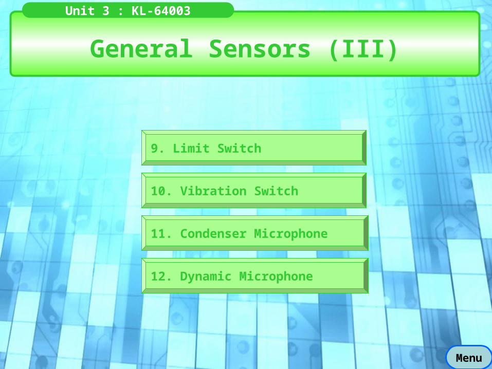
General Sensors (III)
Menu
9. Limit Switch
10. Vibration Switch
11. Condenser Microphone
12. Dynamic Microphone
Unit 3 : KL-64003
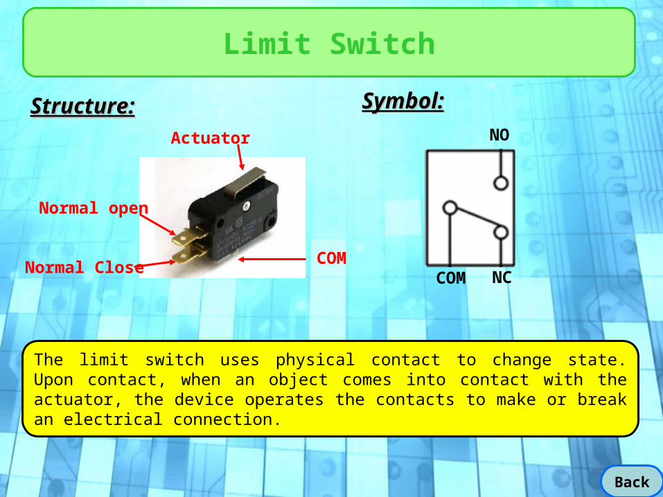
Limit Switch
Back
Structure:Structure: Symbol:Symbol:
The limit switch uses physical contact to change state. Upon contact, when an object comes into contact with the actuator, the device operates the contacts to make or break an electrical connection.
Normal open
Normal Close
NO
NCCOMCOM
Actuator

Circuit Explanation:Circuit Explanation:
When not actuated :
1 = High ; 5 = Low 4 = High ; LED2 OFF 2 = High 3 = Low ; 6 = Low LED1 ON When actuated :
1 = Low ; 6 = Low 4 = Low ; 2 = Low LED2 ON 3 = High ; 6 = High LED1 OFF
(from previous state)

Experiment Procedure:Experiment Procedure:1. Power on the module.2. Press the button to actuate the circuit, what’s the state of the LED? 3. Release the button, what’s the state of the LED?
Answers:Answers: 2. LED1 OFF ; LED2 ON3. LED1 ON ; LED2 OFF

Vibration Switch
Back
Structure:Structure: Symbol:Symbol:
The vibration switch is normally open with vibration springs. When a vibration occurred, the switch changes to close state and the switch turns ON.
Contact:to spring
Contactto metal
Housing
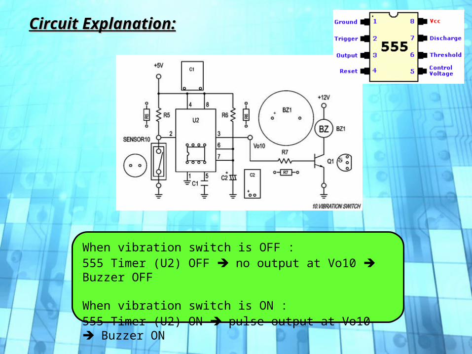
Circuit Explanation:Circuit Explanation:
When vibration switch is OFF :555 Timer (U2) OFF no output at Vo10 Buzzer OFF When vibration switch is ON :555 Timer (U2) ON pulse output at Vo10 Buzzer ON

Experiment Procedure:Experiment Procedure:1. Power on the module.2. What is the status of the buzzer?3. Knock the sensor from side, what is the status of the buzzer?4. Knock the sensor from top, what is the status of the buzzer?
Answers:Answers: 2. Buzzer is OFF3. Buzzer is beeping.4. no response from the buzzer.

Condenser Microphone
Back
Structure:Structure: Symbol:Symbol:
The condenser microphone is constructed with a pair of metal plates that move closer or further apart in response to air vibrations. One rigid plate is connected to ground, the other moving plate is flexible and positively charged by an external voltage. The Condenser microphone is good for crisp sound and can be used for high quality recordings.
GND
Vcc / Audio Signal
VCC
Ground
Audio Out

Circuit Explanation:Circuit Explanation:
The output voltage of the microphone sends to COMMON SPEAKER AMPLIFIER block for signal amplification and driving the speaker.

Experiment Procedure:Experiment Procedure:1. Connects Vo11 (COMDENSER MICROPHONE block) to Vin1
(COMMON SPEAKER AMPLIFIER block). 2. Power on the module.3. Input voice at the microphone, what happened to the speaker? (using
variable resistor R11 to adjust the gain) 4. Blow the microphone and use oscilloscope to record the maximum
amplitude of the waveform at Vo11. (note: this result will be used to compare to the result at next exercise.
Answers:Answers: 3. When rotate right R11, the volume is higher. When rotate left R11, the volume is lower. 4. Max amplitude = 3 Vpp.

Dynamic Microphone
Back
Structure:Structure: Symbol:Symbol:
Dynamic microphones contain a plastic membrane or diaphram. A metal coil inside is connected to the diaphram on one end and a magnet on the other When the diaphram moves in response to air vibrations the coil moves across the magnet creating a current throught induction.
DiaphramGround
Audio Out

Circuit Explanation:Circuit Explanation:
The dynamic microphone converts the sound waves to electric signal at Vo12.

Experiment Procedure:Experiment Procedure:1. Power on the module. 2. Connects Vo12 (DYNAMIC MICROPHONE block) to oscilloscope. 3. Blow the microphone and use oscilloscope to record the maximum
amplitude of the waveform at Vo12. 4. Connects Vo12 to Vin1 ( COMMON SPEAKER AMPLIFIER block) and
input some voice to the microphone. What happened to the speaker?
Answers:Answers: 3. Max amplitude = 15m Vpp.4. Noting happened since the output signal Vo12 is too small.

Gas / Ethanol Sensor
Menu
13. Gas / Smoke Sensor
14. Ethanol Sensor
Unit 4 : KL-64004

Gas / Smoke Sensor
Back
Structure:Structure: Symbol:Symbol:
The sensor resistance RS is serially connected to the load resistance RL to form a voltage divider. The VC provides a stable current through the divider and produces a voltage drop across the RL. If the concentration of gas increases, the output voltage VR will increase due to the decrease of sensor resistance RS (the conductivity of the semiconductor inside the sensor increases). As a result, the output voltage VR is a function of gas concentration.
Housing
NI pin
Stainless steel double gauze
VC
GNDVH
VR
RS
VC: Circuit Voltage Rs: Sensor ResistanceVH: Heating Voltage VR: Load Voltage
RL

Circuit Explanation:Circuit Explanation:
V6V10
V9 = 5 x [R10 / (R9+R10)]
V14
RS
V12
V13
V8
When gas/smoke detected:Sensor Resistance V6 V12 When V12 > V13 positive voltage output at V14 charging C1 when voltage at C1 (V10) > V9 positive output at V8 555 timer triggered pulse output at Vo13When gas/smoke no longer detected:Sensor Resistance V6 V12 When V12 < V13 output LOW at V14 C1 discharging when voltage at C1 (V10) < V9 output LOW at V8 555 timer disabled no pulse output at Vo13

Experiment Procedure:Experiment Procedure:1. With power off, connect Vo13 to Alarm Amplifier SIN. IN2. Power on the module. 3. Use DCV to record the voltage at V9 4. Use DCV to record the voltage at V12 5. Adjust variable resistor R5 so that V13 is 0.5 Volt Higher than V12. 6. Release some gas to the sensor from a lighter. Observe the voltage
change at V12 and V10 7. What is the condition to increase V10? 8. What is the condition for buzzer to start alarming? 9. What is the condition for buzzer to stop alarming? 10. Use smoke instead of gas, and repeat step 6~9.
Answers:Answers: 3. V9 = ~ 1.6V 4. V12 = ~ 1.0V 5. V13 = 1.5V6. V12 increases due to V6 increases (sensor resistance decreases) V10 increases due to V14 increases and charging C17. When V12 > V13, V14 increases and charging C1, so V10 increases8. When V10 (voltage at C1) > V9, V8 will trigger 555 Timer9. When no gas detected, V14 = Low and C1 start discharging. When V10
lower than V9, the alarm will stop.
Note: The answers are used for reference only, the measured voltage is environmental dependent.
Note: If the sensor is not used (unenergized) more than 30 days, the sensor resistance will be very low. It will take couple of minutes for the sensor resistance to increase its normal value.

Ethanol Sensor
Back
Structure:Structure: Symbol:Symbol:
The sensor resistance RS is serially connected to the load resistance RL to form a voltage divider. The VC provides a stable current through the divider and produces a voltage drop across the RL. If the concentration of ethanol increases, the output voltage VR will increase due to the decrease of sensor resistance RS (the conductivity of the semiconductor inside the sensor increases). As a result, the output voltage VR is a function of ethanol concentration.
Housing
NI pin
Stainless steel double gauze
VC
GNDVH
VR
RS
VC: Circuit Voltage Rs: Sensor ResistanceVH: Heating Voltage VR: Load Voltage
RL

Circuit Explanation:Circuit Explanation:
V6V5
V6 = 5 x [R24 / (R23+R24)]
V1
RS
V3
V2
V7
When ethanol detected:Sensor Resistance V6 V3 When V3 > V2 positive voltage output at V1 charging C1 when voltage at C4 (V5) > V6 positive output at V7 555 timer triggered pulse output at Vo14
When ethanol no longer detected:Sensor Resistance V6 V3 When V3 < V2 output LOW at V1 C1 discharging when voltage at C4 (V5) < V6 output LOW at V7 555 timer disabled no pulse output at Vo14

Experiment Procedure:Experiment Procedure:1. With power off, connect Vo14 to Alarm Amplifier SIN. IN2. Power on the module. 3. Use DCV to record the voltage at V6 4. Use DCV to record the voltage at V3 5. Adjust variable resistor R19 so that V2 is 0.5 Volt Higher than V3. 6. Put some ethanol on the tissue and rub the sensor surface. Observe the
voltage change at V3 and V5 7. What is the condition to increase V5? 8. What is the condition for buzzer to start alarming? 9. What is the condition for buzzer to stop alarming? 10.Adjust R19 so that V2 is 1 Volt higher than V3, what do you find?
Answers:Answers: 3. V6 = ~ 1.6V 4. V3 = ~ 1.0V 5. V2 = ~1.5V6. V3 increases due to V6 increases (sensor resistance decreases) V5 increases due to V1 increases and charging C47. When V3 > V2, V1 increases and charging C4, so V5 increases8. When V5 (voltage at C4) > V6, V7 will trigger 555 Timer9. When no ethanol detected, V1 = Low and C4 start discharging. When V5
lower than V6, the alarm will stop. 10. The sensitivity of the sensor becomes lower.
Note: The answers are used for reference only, the measured voltage is environmental dependent.
Note: If the sensor is not used (unenergized) more than 30 days, the sensor resistance will be very low. It will take couple of minutes for the sensor resistance to increase its normal value.

Temperature (AD590) / Humidity Sensor
Menu
15. Temperature (AD590) Sensor
16. Humidity Sensor
Unit 5 : KL-64005

Temperature (AD590) Sensor
Back
Structure:Structure: Symbol:Symbol:
The AD590 is an integrated-circuit temperature transducer which produces an output current proportional to absolute temperature. The device acts as a high impedance constant current regulator, passing 1uA/oK for supply voltages between +4V and +30V. The objective of this module is to convert the 0k scale into 0C so that user can read the value easily.
+
-
Case
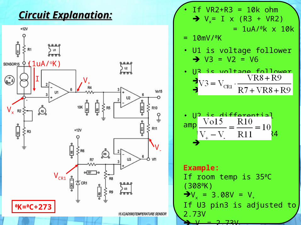
Circuit Explanation:Circuit Explanation:
(1uA/oK)
I
0K=0C+273
V+
V-
VCR1
Vx
• If VR2+R3 = 10k ohm Vx= I x (R3 + VR2) = 1uA/0k x 10k = 10mV/0K
• U1 is voltage follower V3 = V2 = V6
• U3 is voltage follower V3 = V2 = V6
• U2 is differential amplifier When R10/R11=R5/R4
Example: If room temp is 350C (3080K)Vx = 3.08V = V+
If U3 pin3 is adjusted to 2.73V V- = 2.73VVo15 can be obtainedVo15 = (V+ - V-) x 10 = 0.35 x 10 = 3.5 (V) 350C converted to 3.5V

Experiment Procedure:Experiment Procedure:1. Using temperature meter to record the current room temperature. 2. With power off, adjust VR2 so that VR2+R3 is equal to 10k ohm.3. Power on the module. Use DCV to record the voltage Vx (U1 pin3). 4. Adjust variable resistor so that Vf1 is equal to 2.73 Volt.5. Use DCV to record the voltage at Vo15 6. What may be the reasons that cause the errors? 7. Adjust VR2 so that the output at Vo15 fits the current room temperature. 8. Use hair dryer to blow both temperature meter and the sensor. Discuss th
e results. 9. Use graphic interface software to record the temperature from the comput
er.
Answers:Answers: 1. 270C3. Vx = 3.01V ( = 3010k = 301 - 273 0C = 280C )5. Vo15 = 2.93V ( = 29.30C )6. (1) The tolerance of the sensor. i.e. I ≠ 1uA/0k (2) The gain the differential amplifier is not equal to 10 due to the tolerance of the resistor. i.e. R10/R11≠R5/R4 ≠108. The value from the module and temperature fits well after adjusting VR2.
Note: The answers are used for reference only, the measured voltage is environmental dependent.
Note: If you don’t know how to use graphic interface software, please check Unit 0.

Answers:Answers: 9.
Level Setup:
Background color = yellow if measure value < 35Background color = blue if 35 < measure value < 45Background color = pink if measure value > 45
Option Setup:Use TEMP tag

Humidity Sensor
Structure:Structure: Structures:Structures:
Resistive humidity sensors measure the change in electrical impedance of a hygroscopic medium such as a conductive polymer substrate with two separate comb electrodes deposited on. The impedance change is typically an inverse exponential relationship to humidity. Most resistive sensors use symmetrical AC excitation voltage with no DC bias to prevent polarization of the sensor. The resulting current flow is converted and rectified to a DC voltage signal for additional scaling, amplification, linearization, or A/D conversion.
Lead Wires
electrode
substrate
Back

Circuit Explanation:Circuit Explanation: • U6,R28,C3,R27,C2, and resistance at negative feedback loop consists a Wien bridge oscillator. Output frequency =1/2π(R27xR28xC2xC3)1/2 = 256 Hz
• Adjust VR25 for oscillation amplitude.• U5 is inverting amplifier, use VR22 to
reduce output amplitude. • U4 is differential amplifier, use R17 t
o adjust the gain and use R14 to adjust input offset.
• CR2, R20, C1 converts the AC signal into DC level.
• With properly adjusting of the variable resistor in the circuit, the output voltage is able to represent the value of humidity shown below (example):
Voltage 5V 6V 7V 8V 9V 10V
%RH 50 60 70 80 90 100
V+
V-

Experiment Procedure:Experiment Procedure:In this exercise, you need to prepare a humidity meter. 1. Adjust variable resistor R14, R17 and CAL. to center for initial position.
2. Power on the module.3. Use oscilloscope to measure Vf2 and adjust VR25 until Vf2 obtain the
maximum but no distortion oscillation amplitude. 4. Adjust VR22 until U5 pin6 is equal to 1.75 Vpp.5. Use a lead wire to short V+ and V- terminal and adjust VR14 until Vo16 is
equal to DC 10V. 6. Remove the lead wire and connect the lead wires of humidity sensor to V+
and V- terminal. 7. Record the value of the current humidity from humidity meter. 8. Adjust CAL so that the Vo16 is equal to (current humidity value) / 10 Volt.
In this case, Vo16 should be equal to 4.8V.9. Keep breathing out warm air from your mouse/nose to the humidity
sensor, what do you observe? Answers:Answers: 3. Vf2PP= 20V, frequency = 250 Hz.5. Since three are no resistance, we assume this situation is 100%RH7. 48%9. Vo16 keep increasing, but the maximum output voltage will not exceed
10V. (9.6V max = 96%RH)Note: The answers are used for reference only, the measured voltage is environmental dependent.

Infrared / Ultrasonic Sensor
Menu
17. Infrared Sensor
18. Ultrasonic Sensor
Unit 6 : KL-64006

Infrared Sensor
Back
Structure:Structure: Symbol:Symbol:
Infrared emits infrared radiation which is focused by a plastic lens into a narrow beam. The emitting beam of an IR LED is generally proportional to the magnitude of the forward current (forward biased). The beam is modulated i.e. switched on and off, to encode the data. The receiver uses a silicon photodiode to convert the infrared radiation to an electric current for further processing.
Transmitter(Infrared Emitting Diode)
Anode
Cathode
Transmitter Receiver
Receiver(Photodiode)

Circuit Explanation:Circuit Explanation:
Use VR2 to adjusted the output frequency f of the 555 Timer Q1 switches ON and OFF Infrared TX emits ON and OFF If no object blocks between TX and RX Infrared RX receives ON and OFF weak pulse signal input to U2 strong pulse signal (Vpp = 12V, frequency = f) output at Vout_U2 At resonant frequency VLc obtain maximum Vpp signal amplify again though U3 CR1, C5, R13 converts the AC signal into DC signal at U4 pin3 If U4 pin3 > U4 pin2 Vo17 outputs high potential
U2: Inverting amplifier, Gain = ~1000U3: differential amplifier, Gain = ~ 22U4: Comparator, If V+ > V- output = 12V || If V->V+ output = -12V
Vout_U2
Vout_U3VLC

Experiment Procedure:Experiment Procedure:1. Power on the module2. Use oscilloscope to observe the voltage at VLC and adjust the variable
resistor VR2 until Vout_U2 obtain the maximum peak-to-peak voltage.3. Adjust VR3 until U3 pin3 is 0.3V lower than VLC4. Record the voltage at U4 pin2 and U4 pin3 5. Block an object between the sensor, what is the voltage at U4 pin3? 6. What is the value of Vo17 when nothing block the sensor? 7. What is the value of Vo17 when the sensor is blocked by an object? 8. What is the current frequency of the 555 Timer output?
Answers:Answers: 2. VLC = 0.07V3. U3 pin3 = -0.23V4. U4 pin2 = 0.85V ; U4 pin3 = 6V5. U4 pin3 = 0V.6. Vo17 = 11.3V = ON.7. Vo17 = -10.2V = OFF8. Frequency at U1 pin3 = 0.7 kHz~4.7 kHzNote: The answers are used for reference only, the measured voltage is environmental dependent.
Note: Step 2 and 3 are used for calibration. There are several methods for calibrating this circuit. User can use different methods for calibration but still can obtain the same final result.

Ultrasonic Sensor
Back
Structure:Structure: Symbol:Symbol:
Ultrasonic sensors emit and receive a very high frequency sound at 40KHz, which is so high that human can't hear them. Two sensors are identical, but, one as the transmitter and one as the receiver . The transmitter typically sends out a constant beam of sound and the receiver detects any sounds coming in and gives a voltage out.
Transmitter
Receiver
Nominal Frequency: 40kHz

0 0 11
1
0
1
1
0 0
01
1
0
charging C6
When S1 OPEN:
C6 fixed, no oscillation
When S1 CLOSE:
1 1 00
0
1
0
0
1 1
10
0
1
(?) (1)
discharging C6
(0)
U5-a pin2 =0U5-a pin2 =1
U5-a pin3 =1 U5-a pin3 =1U5-d pin13 =0
Charging C6C6 charging/discharging oscillation
Circuit Explanation (Transmitter):Circuit Explanation (Transmitter):
VTX VTX

Receiver Circuit:• Q2 and Q3 forms a cascade amplifier.• U6 is a voltage follower• CR2 and C8 converts the AC signal to a DC voltage.
Circuit Explanation (Receiver):Circuit Explanation (Receiver):
VRX

Experiment Procedure:Experiment Procedure:1. Power on the module2. Put the switch S1 to ON position3. Use variable resistor R18 to adjust the frequency transmitter so that VRX
reaches maximum peak to peak voltage. What is the frequency for at both VTX and VRX point?
4. Use DCV to measure the output voltage Vo18. 5. Put an object to block between the sensor, what is the value of output
voltage Vo18?
Answers:Answers: 3. Frequency at VTX = V RX= 40kHz4. 3.5 Volt5. 0.2 Volt
Note: In step 5, there must be no leakage when blocking an object between the sensor. Since the ultrasonic sensor is very sensitive, if there’s a leakage, the output voltage won’t change too much.

Pressure / Strain Gauge
Menu
19. Pressure Sensor
20. Strain Gauge Sensor
Unit 7 : KL-64007

Pressure Sensor
Back
Structure:Structure: Symbol: Symbol: (Equipment Circuit)(Equipment Circuit)
The pneumatic pressure sensor is based on the piezoresistive (change in conductivity of semiconductors) effect. When a constant-current source is applied to the bridge, the change in resistance will be converted into the change in voltage.
2:Vo+1:GND
GND
+VS
+Vo
4:Vo-
3:+VS
-Vo
P1: Forward Gage
P2:Backward Gage

Circuit Explanation:Circuit Explanation:• Q1 provides fixed current source.• U3 is non-inverting amplifier.
Gain = Vf1/V3 = (1+R13/R12) = 2• U3 is used for output voltage
(Vo19) adjustment.
Since R8 = R14
• U1 and U2 are non-inverting amplifier.
Use VR1 to adjust the current through U1 feedback loop (R3)
Use VR5 to adjust the current through U2 feedback loop (R7)
I
V3
VU26
VU16
When pressure inject into P1+Vo ; -Vo VU16 IR6 VU26 Vo19
When pressure inject into P2+Vo ; -Vo VU16 IR6 VU26 Vo19

Experiment Procedure:Experiment Procedure:1. Power on the module2. Use lead wire to short +Vo and –Vo point.3. Adjust VR1 so that VU26 is equal to 0 volt.4. Disconnect the lead wire between +Vo and –Vo. 5. Adjust VR11 so that Vo19 is close to 1500mV.6. Adjust VR5 for the fine tune so that Vo19 is equal to 1500mV.7. Use bellows to input air pressure to P1. What’s the status of Vo19? 8. Use bellows to input air pressure to P2. What’s the status of Vo19?
Answers:Answers: 7. Vo19 is lower than 1500mV. The higher the input pressure, the lower
the output voltage 8. Vo19 is higher than 1500mV. The higher the pressure, the higher the
output voltage.
bellows

Strain Gauge
Back
Structure:Structure: Symbol: Symbol: (Equipment Circuit)(Equipment Circuit)
The strain gauge is a tiny flat coil of conductive wire that changes its resistance when you bend it. The idea is to place the strain gauge on a beam, bend the beam, and then measure the change in resistance to determine the strain. When applying a force from top, the resistance of the strain gauges at upper beam increase while the resistance of the strain gauge at lower beam decrease.
+5V
Vo-Filament
-5V
ElectrodeVo+
Tension cause resistance increase
Tension cause resistance decrease
Upper beam
Upper beam
Lower beam
Lower beam

Circuit Explanation:Circuit Explanation:
• When applying force from top: Vo+ decreases; Vo- increases
• U4,U5,U6 composes an instrumentation amplifier.
• R22 is used for output voltage adjustment under null weight condition.
• When apply force from the top side of the sensor:
Vo+ Vo-
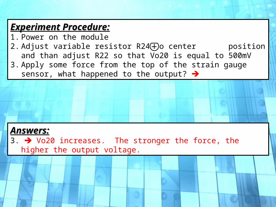
Experiment Procedure:Experiment Procedure:1. Power on the module2. Adjust variable resistor R24 to center position and than adjust R22
so that Vo20 is equal to 500mV 3. Apply some force from the top of the strain gauge sensor, what
happened to the output?
Answers:Answers: 3. Vo20 increases. The stronger the force, the higher the output
voltage.

Hall Current / Proximity Sensor
Menu
21. Hall Current Sensor
22. Proximity Sensor
Unit 8 : KL-64008

Hall Current Sensor
Back
Structure:Structure: Symbol:Symbol:
Hall current sensor, based on Hall Effect technology, provides the output voltage VH proportional to the input current IP (IP = 0~3A VH = 0~4V) if the control current IC is held constant.
GND
V-
Vin-
Vin+
V+ Output
3:V+ (+12V)
1:V- (-12V)
4:Output VH
2:Ground6:Vin-
5:Vin+IP
IP
IC
IC

Circuit Explanation:Circuit Explanation:
The characteristic of the sensor is that with input current is IP 0~3A, the output voltage VH is Vo21 0~4V.
U1 inverting amplifier gain = Vo1/VH =- (R2+VR9) / R1 If gain = 0.75 Vo1:VH = -1:1
U2 is inverting amplifier with gain = 1 Vo1:VH = 1:1
There are 3 offset sources in this circuit: (1) Sensor (2) U1 (3) U2 Using VR3 and VR6 to adjust he offset.
VH

Experiment Procedure:Experiment Procedure:In this exercise, you need to prepare a current supply. 1. Power on the module2. To minimum the offset effect, use lead wire to connect 5:Vin+ and
6:Vin- (zero current input) and adjust VR3 and VR6 so that the output voltage Vo21 is minimum.
3. Disconnect the lead wire between Vin+ and Vin-. 4. Adjust the output current of current supply to minimum. (Important)5. Connect current supply current output I+ to Vin+ and I- to and Vin-.6. Increase the current to 1A and adjust R9 so that Vo21 is 1V.7. Adjust input current to following value and record output voltage Vo21.
(0.25/0.50/0.75/1.0/1.25/1.50/1.75/2.0A )
Answers:Answers: 3. 15mV4. When I = (0.25/0.50/0.75/1.00/1.25/1.50/1.75/2.00) A Vo21 = (0.22/0.48/0.74/1.00/1.26/1.51/1.76/2.02) V Good linearity.
Note: The answers are used for reference only, the measured voltage is environmental dependent.
Note: The input current do NOT exceed 3.0 A

Proximity Sensor
Back
Structure:Structure:
Inductive proximity sensors are widely used in various applications to detect metal devices. They consist of an oscillator, trigger, and switching amplifier. If a metal object enters the electromagnetic field of the oscillator coil, eddy currents are induced in this coil which change the amplitude of oscillation, which causes the trigger stage to trip and the semiconductor output stage to switch.
LED: Indicator
Detect HeadVCC
Output
GND
Symbol: Symbol: (Equipment Circuit)(Equipment Circuit)
Oscillator Trigger SwitchingAmplifier

Circuit Explanation:Circuit Explanation:
When no metallic object approach to the detecting head:Vo = High Vo22 = Low Q1 OFF Buzzer OFF
When a metallic object approach to the detecting head:Vo = LOW Vo22 = High Q1 ON Buzzer ON
Vo

Experiment Procedure:Experiment Procedure:1. Insert proximity sensor to 3 pin module socket. 2. Power on the module3. Use different type of object to approach to the detecting head and
observe the result.
Answers:Answers: 3. When metallic type object close to the detect head, buzzer ON.

CDS / Photovoltaic Sensor
Menu
23. CDS Sensor
24. Photovoltaic
Unit 9 : KL-64009

CDS Sensor
Back
Structure:Structure: Symbol:Symbol:
CaDmium Sulphide (CDS) cells, sometimes called photoresistors or photoconductive cells, rely on the material's ability to vary its resistance according to the amount of light striking the cell. The more light that strikes the cell, the lower the resistance.
LeadWires
CaDmium Sulphide(Orange part)
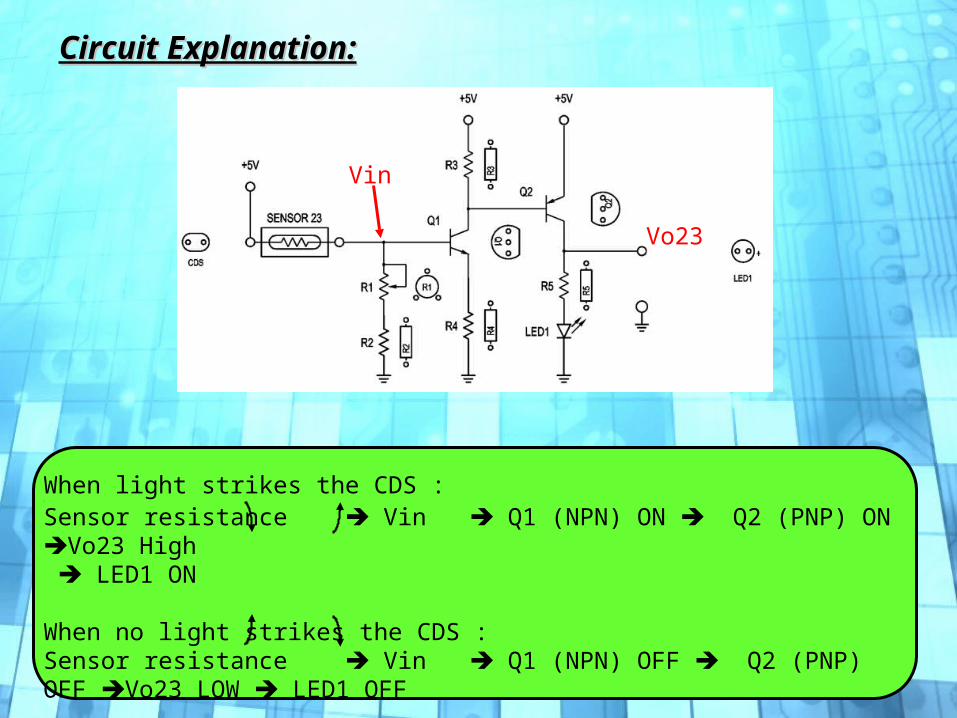
Circuit Explanation:Circuit Explanation:
When light strikes the CDS :.
Sensor resistance Vin Q1 (NPN) ON Q2 (PNP) ON Vo23 High LED1 ON When no light strikes the CDS :Sensor resistance Vin Q1 (NPN) OFF Q2 (PNP) OFF Vo23 LOW LED1 OFF
Vin
Vo23

Experiment Procedure:Experiment Procedure:1. Power on the module2. Block the CDS and adjust variable resistor R1 make the LED1 just from
the bright to dark. 3. What is the status of the LED1 when the light strikes the CDS? And
what is the voltage at Vin? 4. What is the status of the LED1 when the CDS is blocked? And what is
the voltage at Vin? 5. Use oscilloscope to observe the voltage at Vin, what is the response time when
block and unblock the CDS?
Answers:Answers: 3. The LED1 is ON and Vin = 3.6 V4. The LED1 is OFF and Vin = 0.1V5. Unblock to block: response time = 150ms Block to unblock: response time = 100ms
unblock
block
unblock
Note: The answers are used for reference only, the measured voltage is environmental dependent.

Photovoltaic Sensor
Back
Structure:Structure: Symbol:Symbol:
Photovoltaic, or PV for short, is a technology in which light is converted into electrical power without the aid of any external excitation power. The magnitude of its light-sensitive electrical output signal (current or voltage) is directly proportional to the light intensity it’s exposed to.
Photovoltaic CellPhotovoltaic Module

Circuit Explanation:Circuit Explanation:
U1 IV Conversion (Vo1 = Ish x (R6+VR7) If (R6+VR7) is adjusted properly, Vo1 = 0.001V / LxR8, C1 Low Pass Filter out of 100 or 120 Hz flicker from fluorescent lamp)
U2 Voltage follower
Ish
Vo1
(Fluorescent lamps which operate directly from mains frequency AC will flicker at twice the mains frequency, since the power being delivered to the lamp drops to zero twice per cycle. This means the light flickers at 120 times per second (Hz) )

Answers:Answers: 4.
5. The output voltage increases, meaning that the lumen increases.
Experiment Procedure:Experiment Procedure:1. Power on the module2. If you have a illuminometer, check the current lumen. We assume that
the current lumen is 500 lx.3. Adjust variable resistor so that Vo24 is equal to 0.5V.4. Use oscilloscope to compare the waveform at Vo1 and Vo24.5. Move the sensor close to the light source, what happened to Vo24?6. Use graphic interface software to record the measured lumen.
Note: The answers are used for reference only, the measured voltage is environmental dependent.
Vo1Vrms = 0.5V120Hz
Vo24

Answers:Answers: 6.
Level Setup:
Background color = yellow if measure value < 1000Background color = blue if 1000 < measure value < 2000 Background color = pink if measure value > 2000
Option Setup:Use LUX tag

V/F Converter
Menu
25. V/F Converter
Unit 10 : KL-64010
V/F Converter
Back
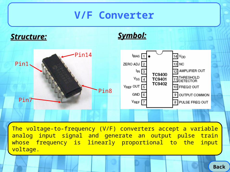
Structure:Structure: Symbol:Symbol:
The voltage-to-frequency (V/F) converters accept a variable analog input signal and generate an output pulse train whose frequency is linearly proportional to the input voltage.
Pin1
Pin7
Pin8
Pin14
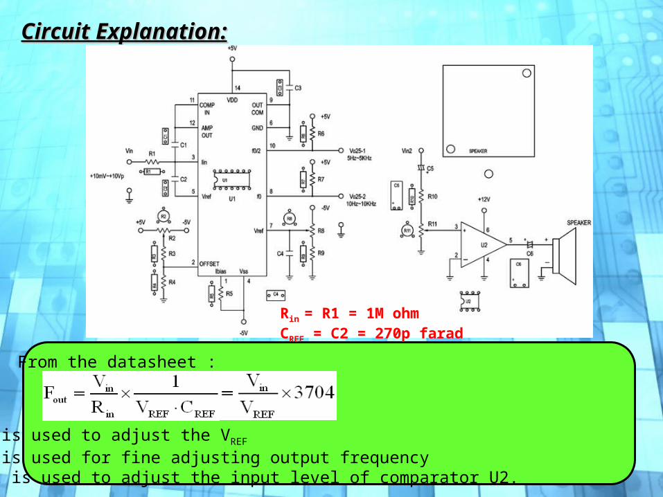
Circuit Explanation:Circuit Explanation:
Rin = R1 = 1M ohmCREF = C2 = 270p farad
From the datasheet :
VR8 is used to adjust the VREF
VR2 is used for fine adjusting output frequencyVR11 is used to adjust the input level of comparator U2.

Experiment Procedure:Experiment Procedure:1. Power on the module.2. Adjust variable resistor R8 until pin7 of the U1 is equal to -4 Volt.3. On the KL62001 main unit, connect VR3 to GND, VR1 to +5V, and VR2
connects to Vin. 4. Use DCV to measure the Vin and adjust the potentiometer until Vin is
equal to 1V. 5. From the formula with VREF = 4V and Vin = 1V, we can obtain that
Fout (Vo25-2) = 926 Hz Fout/2 (Vo25-1) = 463 Hz6. Use oscilloscope to measure Vo25-1. Adjust variable resistor R2 until
the output frequency is equal to 463 Hz Calibration Complete7. Use oscilloscope to record Vo25-1 and Vo25-2. 8. Adjust VR2 on the main unit so that Vin is equal to 2V9. Compare the result by using formula and oscilloscope. 10. Connect Vo25-1 to Vin2, what happened to the speaker? 11.Connect Vo25-2 to Vin2, what happened to the speaker?
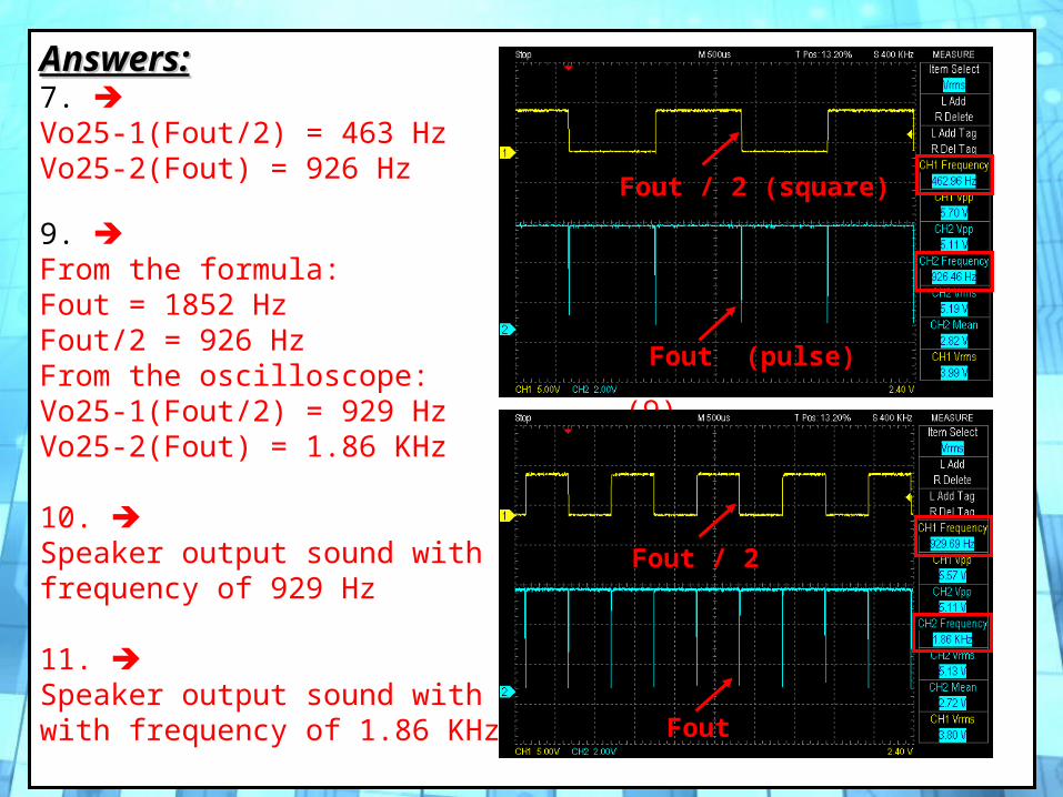
Answers:Answers: (7).7. Vo25-1(Fout/2) = 463 HzVo25-2(Fout) = 926 Hz
9. From the formula:Fout = 1852 HzFout/2 = 926 HzFrom the oscilloscope:Vo25-1(Fout/2) = 929 Hz (9).Vo25-2(Fout) = 1.86 KHz
10. Speaker output sound withfrequency of 929 Hz
11. Speaker output sound withwith frequency of 1.86 KHz
Fout (pulse)
Fout / 2 (square)
Fout
Fout / 2

F/V Converter
Menu
26. V/F Converter
Unit 11 : KL-64011

F/V Converter
Back
Structure:Structure: Symbol:Symbol:
The frequency-to-voltage (F/V) converters accept any input frequency waveform and provides a linearly-proportional voltage output.
Pin1
Pin7
Pin8
Pin14
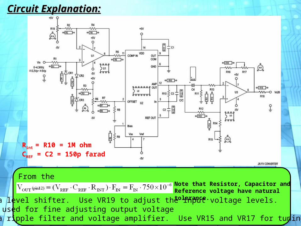
Circuit Explanation:Circuit Explanation:
From the datasheet :
U1 is a level shifter. Use VR19 to adjust the input voltage levels. VR2 is used for fine adjusting output voltageU3 is a ripple filter and voltage amplifier. Use VR15 and VR17 for tuning.
Rint = R10 = 1M ohmCREF = C2 = 150p farad
Note that Resistor, Capacitor and Reference voltage have natural tolerance.

Experiment Procedure:Experiment Procedure:In this exercise, you need to prepare a function generator. 1. Power on the module.2. Adjust variable resistor R19 to center for initial position.3. Use a lead wire to connect Vin and Ground.4. Since there are no signal input to the converter, the output voltage shou
ld be zero. So adjust variable resistor R6 until Vo26 is equal to 0 V. 5. Disconnect the test lead and Input a 4.3kHz, 2VPP Sine wave to the Vin.6. Adjust R15 and R17 until Vo26 is equal to DC 4.3V (observe by DCV) a
nd the sawtooth ripple is minimized (observe by oscilloscope, use AC coupling, scale = 100mV). Both conditions should be satisfied. Calibration Complete.
7. Change the input frequency to 500/1000/1500/2000/2500/3000/3500 and 4000 Hz. What are the corresponding output voltage?
Answers:Answers: 7. Vin (Hz) 500 1000 1500 2000 2500 3000 3500
Vo26 (V) 0.498 1.000 1.501 2.003 2.501 3.002 3.504
Good Linearity
Note: If no input signal detected, use VR19 for input level adjust.

Temperature (PT100) Sensor
Menu
27. Temperature (PT100) Sensor
Unit 12 : KL-64012

Temperature (PT100) Sensor
Structure:Structure: Symbol:Symbol:
PT-100 is one form of the RTD (Resistance Temperature Detector). It is made of the platinum wire and has the resistance of 100 ohm at 00C. The resistance vs. temperature characteristic of PT-100 can be expressed as:
RT = 100 (1+0.00392T)
If constant current I of 2.55mA flow through PT-100
VB’ = I x RT = (255+T)mV
Stainless-steel protection tube(Platinum wired wound inside)
A
B
B’
B=B’A
B
B’
Current In
Voltage Out
Back

Circuit Explanation:Circuit Explanation:
• VR2 is used to control the constant current source to 2.25mV• U1 is non-inverting amplifier
V16= (2550+10T) mV• U2 is differential amplifier• U3 is voltage follower Adjust VR14 to control Vf1 (offset of U2)• So if Vf1 = 2550mV Vo27 = 100T mV Conversion Ratio = 100mV / 0C.
VB’ V16 Vo27
VB’ = (255+T)mVV16 = (2550+10T)mV
Vf1
V27 = 100T mV

Experiment Procedure:Experiment Procedure:In this exercise, you need to prepare a thermometer (mercury) for calibration. 1. Using thermometer to record the current room temperature (T). 2. Connect 2 lead wires (white) to B and B’, and lead wire (red) to A.3. Power on the module. 4. Adjust VR2 until VB’ = (255+T)mV 5. Adjust VR14 until Vo27 is equal to T/10 V (Calibration complete) 6. Put both PT-100 and the mercury thermometer inside hot water. 7. What is the value shown on the mercury thermometer? 8. What is the output voltage of Vo27? 9. Put both PT-100 and the mercury thermometer inside cold water.10. What is the value shown on the mercury thermometer? 11. What is the output voltage of Vo27? 12. What’s the difference between AD590 and PT100 temperature sensor?
Answers:Answers: 1. 270C4. VB’ = 282mV5. Vo27 = 2.70V7. 54.30C 8. 5.45 Volt (=54.50C)10. 110C 11. 1.05 Volt (=10.50C)12. The response time of PT100 is much slower than AD590.
Note: The answers are used for reference only, the measured voltage is environmental dependent.
Level (Water) Sensor
Menu
28. Level (Water) Sensor
Unit 13 : KL-64012
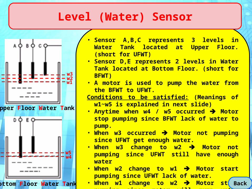
• Sensor A,B,C represents 3 levels in Water Tank located at Upper Floor. (short for UFWT)
• Sensor D,E represents 2 levels in Water Tank located at Bottom Floor. (short for BFWT)
• A motor is used to pump the water from the BFWT to UFWT.
Conditions to be satisfied: (Meanings of w1~w5 is explained in next slide)
• Anytime when w4 / w5 occurred Motor stop pumping since BFWT lack of water to pump.
• When w3 occurred Motor not pumping since UFWT get enough water.
• When w3 change to w2 Motor not pumping since UFWT still have enough water
• When w2 change to w1 Motor start pumping since UFWT lack of water.
• When w1 change to w2 Motor still pumping since motor will pump until water reach HIGH level
• When w2 change to w3 Motor stop pumping since UFWT got enough water.
Upper Floor Water Tank
Bottom Floor Water Tank
w1w2w3
w4w5
Back
Level (Water) Sensor
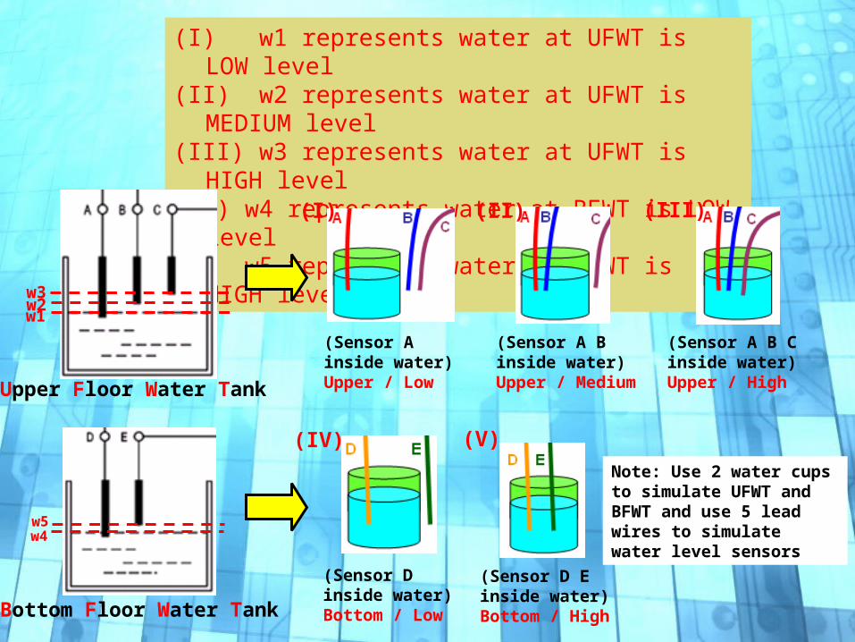
(I) w1 represents water at UFWT is LOW level (II) w2 represents water at UFWT is MEDIUM level (III) w3 represents water at UFWT is HIGH level (IV) w4 represents water at BFWT is LOW level (V) w5 represents water at BFWT is HIGH level
Upper Floor Water Tank
w1w2w3
Bottom Floor Water Tank
w4w5
(Sensor A B C inside water)Upper / High
(Sensor A B inside water)Upper / Medium
(Sensor A inside water)Upper / Low
(Sensor D E inside water)Bottom / High
(Sensor D inside water)Bottom / Low
(I) (II) (III)
(IV) (V)
Note: Use 2 water cups to simulate UFWT and BFWT and use 5 lead wires to simulate water level sensors
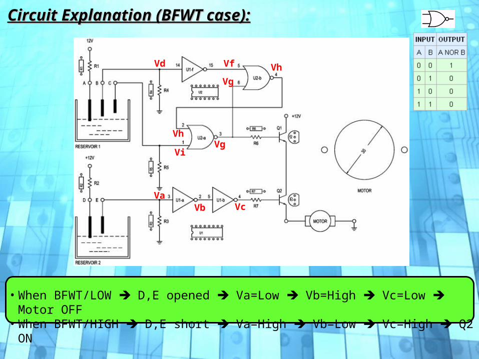
Circuit Explanation (BFWT case):Circuit Explanation (BFWT case):
• When BFWT/LOW D,E opened Va=Low Vb=High Vc=Low Motor OFF• When BFWT/HIGH D,E short Va=High Vb=Low Vc=High Q2 ON
VaVb Vc
Vd Vf
Vg
Vh
Vi
Vh
Vg
Circuit Explanation (UFWT case):Circuit Explanation (UFWT case):
• When UFWT/HIGH A,B,C short Vd=High, Vi=High Vf=Low, Vg=Low Vh=High Q1 OFF Motor OFF
• When UFWT/HIGH >MEDIUM A,B short Vd=High, Vi=Low Vf = Low Vg=Low since Vh=High from previous status Q1 OFF Motor OFF
• When UFWT/MEDIUM > LOW A,B,C open Vd=Low, Vi=Low Vf=High Vh=Low Vg=High Q1 ON Motor ON if Q2 ON
• When UFWT/LOW > MEDIUM A,B short Vd High, Vi=Low Vf = Low Vg=High since Vh=Low from previous status Q1 ON Motor still ON if Q2 ON
• When UFWT/MEDIUM>HIGH A.B.C short Vd=High, Vi=High Vf=Low, Vg=Low Q1 OFF Motor OFF
Va Vb Vc
Vd Vf
Vg
Vh
Vi
Vh
Vg

Experiment Procedure:Experiment Procedure:In this exercise, you need to prepare 5 lead wires to simulate A/B/C/D/E sensors and 2 water cups to
simulate Upper and Bottom water tank. 1. Use 3 lead wires to connect A,B, and C terminals and put the other end of the three lead wires inside water cup (Upper Tank). Note that all three ends need to be entirely under water. 2. Use 2 lead wires to connect D,E terminals and put the other end of the two lead wires inside another water cup (Bottom Tank). Note that both ends need to be entirely under water. 3. Power on the module, what’s the status of the motor? 4. Remove lead wire C from upper cup, what’s the status of the motor? 5. Remove lead wire B from upper cup, what’s the status of the motor? 6. Remove lead wire E from bottom cup, what’s the status of the motor? 7. Put lead wire E back to the bottom cup, what’s the status of the motor? 8. Put lead wire B back to the upper cup, what’s the status of the motor? 9. Put lead wire C back to the upper cup, what’s the status of the motor?
Answers:Answers: 3. Motor OFF (UFWT full, no need pumping)4. Motor OFF (UFWT still have enough water, no need pumping)5. Motor ON (UFWT lacks water, need pumping water from BFWT)6. Motor OFF (BFWT lack of water to pump to UFWT)7. Motor ON (BFWT got enough water to pump to UFWT)8. Motor ON (Once starts pumping, motor pumps until water reach HIGH level)9. Motor OFF (UFWT full, no need pumping)

Fiber Optics
Menu
29. Fiber Optics
Unit 14 : KL-64014
Fiber Optic
Back
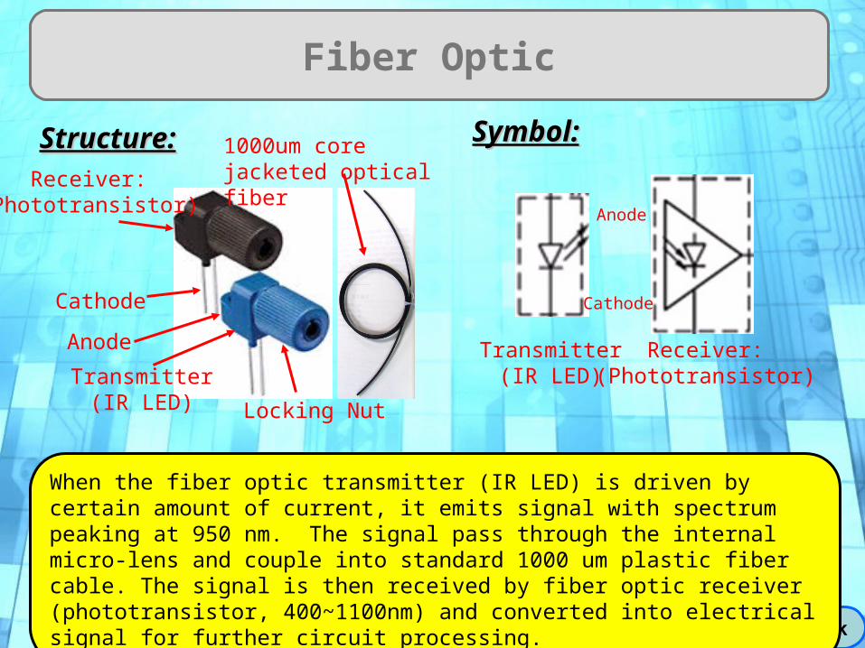
Structure:Structure: Symbol:Symbol:
When the fiber optic transmitter (IR LED) is driven by certain amount of current, it emits signal with spectrum peaking at 950 nm. The signal pass through the internal micro-lens and couple into standard 1000 um plastic fiber cable. The signal is then received by fiber optic receiver (phototransistor, 400~1100nm) and converted into electrical signal for further circuit processing.
Anode
Cathode
Transmitter(IR LED)
Receiver:(Phototransistor)
1000um core jacketed optical fiber
Transmitter(IR LED)
Receiver:(Phototransistor)
Locking Nut
Cathode
Anode
Circuit Explanation:Circuit Explanation:
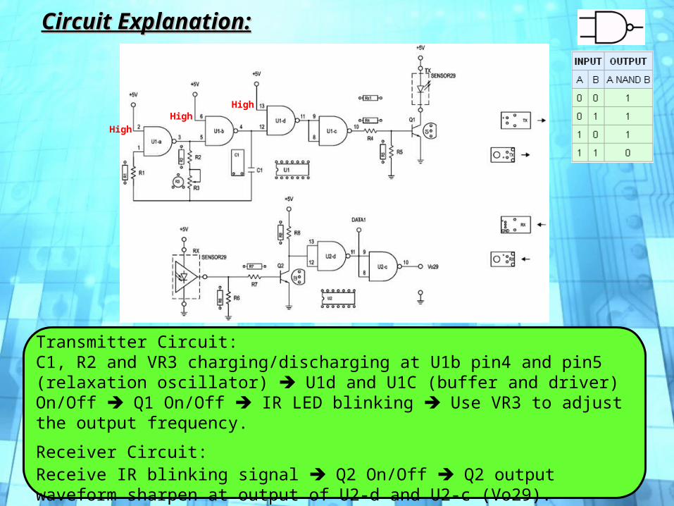
Transmitter Circuit:C1, R2 and VR3 charging/discharging at U1b pin4 and pin5 (relaxation oscillator) U1d and U1C (buffer and driver) On/Off Q1 On/Off IR LED blinking Use VR3 to adjust the output frequency.
Receiver Circuit:Receive IR blinking signal Q2 On/Off Q2 output waveform sharpen at output of U2-d and U2-c (Vo29).
High
HighHigh

Experiment Procedure:Experiment Procedure:1. Cut off the ends of the optical fiber with a single edge razor blade or sharp knife.
Try to obtain a precise 90 degree angle. 2. Insert the fiber through the transmitter and receiver locking nut and into the
connector until the core tip seats against the internal micro-lens.3. Screw the connector locking nut down to a snug fit, locking the fiber in place.4. Power on the module.5. Connect CH1 of the oscilloscope to the cathode of the transmitter. What is the
shape of waveform? 6. Adjust VR3 until the frequency at cathode of the transmitter is equal to 2kHz. 7. Connect CH2 of the oscilloscope at DATA1, what’s the frequency? 8. Connect CH2 of the oscilloscope at Vo29, what’s the frequency?
Answers:Answers: 5. Square wave (4.5Vpp)7. 2kHz (inverting) 8. 2kHz (non-inverting)

LVDT
Menu
30. LVDT
Unit 15 : KL-64015

LVDT
Back
Structure:Structure: Symbol:Symbol:
Linear Variable Differential Transformer comprises 1 primary coil and 2 secondary coils. When primary coil is energized by a constant amplitude AC source, the magnetic flux thus is coupled by the core to the adjacent secondary coils. The voltage developed at the secondary coils S1,S2 depend on the position of the core. When the core is located at the center (Null Point), VS1=VS2. When the core is located close to the S1 side, more flux is coupled to S1 side, VS1>VS2, and vice versa.
Stainless Steel Housing
Knob
Ferromagnetic Core
S1
S2
P
Note: The optimum operating frequency for the LVDT using in KL64015 is 350Hz at 5Vrms (14.14Vpp)

Circuit Explanation:Circuit Explanation:
• U1,R1,C1,R2,C2, and resistance at negative feedback loop consists a Wien bridge oscillator. Output frequency =1/2π(R1xR2xC1xC2)1/2 = 338.6Hz for energized AC source.
• R3,R4, VR5, R6 determine the output amplitude. • CR1 and CR2 are used to improve the stability of the output amplitude.• Q1 and Q2 are used to improve the driver ability. • CR3, C4, R10 and CR4, C5, R11 convert the AC output voltage to DC. • U2 and U3 are voltage followers which are used as buffers.
S1
S2
P

Experiment Procedure:Experiment Procedure:1. Power on the module.2. Connect oscilloscope CH1 to P terminal and adjust VR5 so that the voltage Vp i
s equal to 14Vp-p. What is the frequency of the excitation energy of LVDT?3. Adjust the knob until DC voltage of Vo30-1 and Vo30-2 are equal.4. Connect oscilloscope CH1 to S1 and CH2 to S2 terminal, what do you find? 5. Use ruler to measure the total visible length of the screw. What is the outside le
ngth of the screw now? 6. Try to draw the relation between the position of the core and output voltage. 7. What is the resolution of this LVDT?
Answers:Answers: 2. 338 Hz.3. Vo30-1 = Vo30-2 = 6.2V, the core is located at Null point now.4. Two waveforms are identical (Vpp = 14V, f = 338Hz)5. Length = ~ 4mm
Note: The answers are used for reference only, the measured voltage is environmental senst\itive

Answers:Answers:
6.
7. +0.25V/ mm for Vo30-1 - 0.33V/ mm for Vo30-2
Null point 4.8mm
Rotation Angle Sensor
Menu
31. Rotation Angle Sensor
Unit 16 : KL-64016
Rotation Angle Sensor
Back
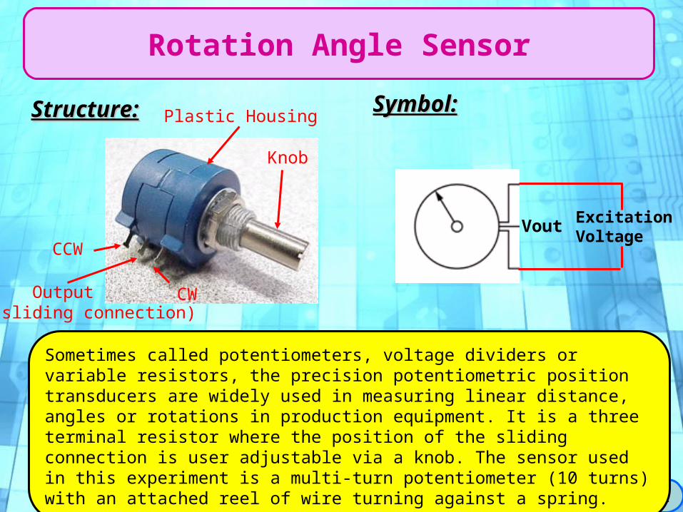
Structure:Structure: Symbol:Symbol:
Sometimes called potentiometers, voltage dividers or variable resistors, the precision potentiometric position transducers are widely used in measuring linear distance, angles or rotations in production equipment. It is a three terminal resistor where the position of the sliding connection is user adjustable via a knob. The sensor used in this experiment is a multi-turn potentiometer (10 turns) with an attached reel of wire turning against a spring.
ExcitationVoltage
Vout
Knob
Plastic Housing
CW
CCW
Output(sliding connection)

Circuit Explanation:Circuit Explanation:
• U1 (Buffer Amplifier) provides a precision reference voltage at Vf1.• U2 (Buffer Amplifier) transfers the voltage from U2pin3 to U2pin6.• U4 (Buffer Amplifier) provides fix voltage (adjusted by VR7) at U4pin6 to
control the current flow through feedback loop to obtain a stable output at Vo31.

Experiment Procedure:Experiment Procedure:1. Power on the module2. Adjust variable resistor VR7 to center for initial position.3. Rotate the potentiometer from most CCW to most CW position. How
many turns is built in the potentiometer? 4. How many degrees you have rotate in step 2? 5. Fix the potentiometer at 36000 Adjust the variable resistor VR2 until
Vo31 is equal to 3.600V.6. Rotate the potentiometer in CCW direction for 5 turns. Adjust the
variable resistor VR7 until Vo31 is equal to 1.800V. 7. Measure and record the output voltage Vo31 for each following turn
values. 1/2/3/4/5/6/7/8/9/10 turns
Answers:Answers: 3. 10 turns4. 36000
5.
Turns1
3600
2
7200
3
10800
4
14400
5
18000
6
21600
7
25200
8
28800
9
32400
10
36000
Vo31 (V) 0.359 0.719 1.079 1.440 1.802 2.162 2.522 2.882 3.241 3.601
Good Linearity