Embed Size (px)
Citation preview

The best solution for PCB manufacturing test
– More accuracy and R&R – More languages supported – More ESD robustness
Keysight E5063A ENA Series PCB Analyzer
Technical Overview

Why Choose the E5063A PCB Analyzer for Your Toughest Printed Circuit Board Measurement Challenges?
As the operating speed of electronic circuits increase, signal integrity of printed circuit boards (PCBs) drastically affect per-formance and there is an increasing requirement for controlled impedance PCBs. In addition, with the proliferation of wireless devices, such as smartphones and tablets, there is a trend to integrate antennas onto PCBs. Therefore, in addition to the traditional time domain impedance measurement, there is a growing need to measure the frequency domain response of PCB integrated antennas.
The E5063A PCB Analyzer consists of a E5063A ENA Vector Network Analyzer with Option 011 (Time domain analysis/Test Wizard). The E5063A provides frequency domain measurement capability and Option 011 adds time domain analysis capability, as well as a dedicated graphical user interface for PCB manufacturing test.
The number of available ports can be expanded up to four with the addition of U1810B USB coaxial switches, to allow for simultaneous connection to both single-ended and differential probes.
Key features and benefits – Up to 18 GHz of bandwidth with 24.8 ps rise time enables measurement on the
latest PCB designs
– Unmatched performance – Wide dynamic range to observe the true performance of your DUT: > 100 dB
(at 4.5 GHz) – Low noise floor for accurate and repeatable measurements: 75 μVrms – Fast measurement speed for real-time analysis: 154 msec (at 1601 points
with full 2-port calibration performed)
– State-of-the art error correction techniques reduce measurement errors – Automatic deskew ensures easy removal of fixture and probe effects – Full calibration (ECal) available for the utmost in measurement accuracy
– Upgrade all available ENA hardware and software options at any time. Buy what you need today and protect your investment by upgrading later when requirements change.
Speed, accuracy and ease-of-use you need to ramp up rapidly and optimize PCB manufacturing test.
The E5063A PCB Analyzer changes the world of PCB measurements.
02 | Keysight | E5063A ENA Series PCB Analyzer - Technical Overview
www.keysight.com/find/vnawww.keysight.com/find/vna

Three breakthroughs for PCB manufacturing test
Compared to traditional solutions based on TDR Oscilloscopes, the E5063A PCB Analyzer provides:
– More accuracy and R&R (Repeatability & Reproducibility) – More languages supported – More ESD robustness
More accuracy and R&R
Delivers new standards in accuracy
– Low noise floor for accurate and repeatable measurements
– State of the art error correction techniques enables you to measure your device, not your measurement system
More languages supported
An analyzer that speaks the user’s language
– Since there are many cases where tasks are solved more efficiently in one’s native language, a multi-lingual user interface is provided.
– Currently available languages include English, Simplified and Traditional Chinese, Japanese, and Korean
More ESD robustness
Protection circuits implemented inside the instrument
– Proprietary electrostatic discharge (ESD) protection chip significantly increases ESD robustness, while at the same time maintaining excellent RF performance
– Highly robust architecture can minimize instrument failure from ESD and free you from worrying about instrument repair fees and downtime
E5063A ENA Series PCB Analyzer the Best Solution for PCB Manufacturing Test
03 | Keysight | E5063A ENA Series PCB Analyzer - Technical Overview
www.keysight.com/find/vna

E5063A ENA Series PCB Analyzer the Best Solution for PCB Manufacturing Test
The PCB Analyzer user interface is designed specifically for measuring controlled impedance and return loss on PCBs. Providing a similar look-and-feel to traditional solutions, the PCB Analyzer is easy to setup and use without the need for extensive operator training.
Edit test modeTest files are easily created and modified via the integrated test file editor. Most files can be created with just a few mouse clicks. Test files provide a convenient method for automated testing of boards with a number of different controlled impedance traces.
Execute test modeSimple and intuitive user interface for non-technical operators. All the information necessary for performing measurements is stored in a test file. An operator only needs to select the appropriate test file from a list and the system is ready for testing.
04 | Keysight | E5063A ENA Series PCB Analyzer - Technical Overview
www.keysight.com/find/vna

WizardsSetup and Error Correction Wizards allows for intuitive and error free setup, error correction, and measurements.
Dedicated controls for common adjustments
– The vertical and horizontal scales can be optimized by using the software knobs. In addition, the horizontal units can be set to display either time or distance (English or metric units).
– The DUT Length Wizard automatically measures the DUT length. The DUT length setting is used to set the optimum time span for measurements. After the time span is set, the test limits can be defined as a percentage of the trace length. Absolute, average, or multi-segment limit types are available.
E5063A ENA Series PCB Analyzer the Best Solution for PCB Manufacturing Test
05 | Keysight | E5063A ENA Series PCB Analyzer - Technical Overview
www.keysight.com/find/vna

Three Breakthroughs for PCB Manufacturing Test
More accuracy and R&RAccurate, repeatable, and reproducible measurements are important to ensure measurement correlation between the OEM and fabricator, as well as increasing yield.
There are two main considerations:absolute accuracy of measurement and measurement R&R (Repeatability and Reproducibility).
A number of factors can influence accuracy and R&R: cables, fixtures and probes, test equipment and operators.
Error correction is a powerful technique to remove systematic errors due to the cables, fixtures and probes, and test equipment.
State of the art error correction tech-niques reduce measurement errors and allows the PCB Analyzer to deliver new standards in accuracy required for the latest generation of products.
If there is measurement error, one may be left in doubt about the acceptability of the product.
Guard bands are often used to account for measurement error, but results in lower yield.
Lowerlimit
Upperlimit
Value
PASSFAIL FAIL
Value
PASS IAFLIAF L
Uncertainty Uncertainty
Lowerlimit
Upperlimit
Value
PASSFAIL FAIL
Guardband Guardband
Lowerlimit
Upperlimit
If there is no measurement error, one can distinguish between good and bad products with confidence.
06 | Keysight | E5063A ENA Series PCB Analyzer - Technical Overview
www.keysight.com/find/vna

Three Breakthroughs for PCB Manufacturing Test
Choose your level of accuracy – trade off between complexity and accuracyOver the years, many different approaches have been developed for removing the effects of the test fixture and probes from the measurement. The level of difficulty for each error correction technique is related to the accuracy of each method. It is important to have a test system that will allow flexibility of choosing the method of error correction desired for each application.
– Deskew (also known as Port Extension) mathematically extends the calibration reference plane to the DUT, effectively removing the delay from the test setup. This technique is easy to use, but assumes the probe and fixture – the unwanted structure – looks like a perfect transmission line: a flat magnitude response, a linear phase response, and constant impedance. If the probe and fixture are very well designed, this technique can provide good results.
– Deskew and loss compensation mathematically extends the calibration reference plane to the DUT, effectively removing the delay and loss from the test setup. This technique is a good compromise between level of difficulty and accuracy.
– Full calibration (SOLT) is one of the most comprehensive calibrations. This calibration effectively removes delay, loss, and mismatch from the test setup, making it possible to perform measurements with the highest possible accuracy.
– Electronic calibration (Ecal) is a complete solid-state calibration solution which makes full calibration fast and easy. Traditional mechanical calibrations require intensive operator interaction which is prone to errors. With ECal, the operator simply connects the ECal module to the instrument and the software controls the rest.
Error correction techniques
Level of difficulty
Accuracy
Easiest
Mostaccurate Full calibration
(SOLT)
Deskew andloss compensation
Deskew(port extension)
Full calibration(ECal)
Error correction
07 | Keysight | E5063A ENA Series PCB Analyzer - Technical Overview
www.keysight.com/find/vna

Three Breakthroughs for PCB Manufacturing Test
Since there are many cases where tasks are solved more efficiently in one’s native language, a multi-lingual user interface is provided.
Currently available languages include English, Simplified and Traditional Chinese, Japanese, and Korean.
In applications such as PCB testing, large static charges can be stored in the DUT.
Special care is required when using traditional instruments in such situations, to make sure that the instrument is not damaged by electrostatic discharge (ESD). Vulnerability to ESD can lead to increased maintenance fees and long repair times.
The E5063A PCB Analyzer is designed for high robustness against ESD by implementing protection circuits inside the instrument.
Leveraging the company’s expertise in RF design, Keysight Technologies, Inc. has invested in key technology blocks like our proprietary ESD protection chip to significantly increase ESD robustness, while at the same time maintaining excellent RF performance.
More ESD robustness
ESD survival IEC 801-2 Human Body Model. (150 pF, 330 Ω) RF Output Center pins tested to 3 kV, 10 cycles
More languages supported
An analyzer that speaks your language
08 | Keysight | E5063A ENA Series PCB Analyzer - Technical Overview
www.keysight.com/find/vna
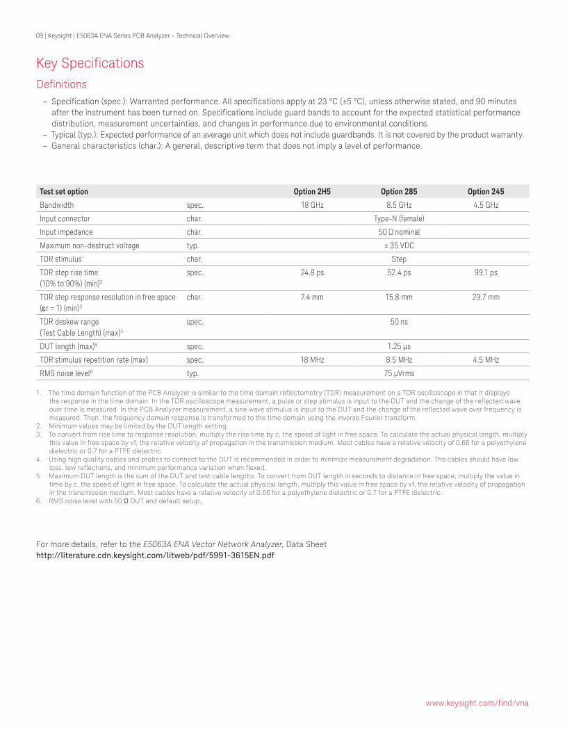
Key SpecificationsDefinitions
– Specification (spec.): Warranted performance. All specifications apply at 23 °C (±5 °C), unless otherwise stated, and 90 minutes after the instrument has been turned on. Specifications include guard bands to account for the expected statistical performance distribution, measurement uncertainties, and changes in performance due to environmental conditions.
– Typical (typ.): Expected performance of an average unit which does not include guardbands. It is not covered by the product warranty. – General characteristics (char.): A general, descriptive term that does not imply a level of performance.
For more details, refer to the E5063A ENA Vector Network Analyzer, Data Sheethttp://literature.cdn.keysight.com/litweb/pdf/5991-3615EN.pdf
Test set option Option 2H5 Option 285 Option 245
Bandwidth spec. 18 GHz 8.5 GHz 4.5 GHz
Input connector char. Type-N (female)
Input impedance char. 50 Ω nominal
Maximum non-destruct voltage typ. ± 35 VDC
TDR stimulus1 char. Step
TDR step rise time (10% to 90%) (min)2
spec. 24.8 ps 52.4 ps 99.1 ps
TDR step response resolution in free space (εr = 1) (min)3
char. 7.4 mm 15.8 mm 29.7 mm
TDR deskew range (Test Cable Length) (max)4
spec. 50 ns
DUT length (max)5 spec. 1.25 μs
TDR stimulus repetition rate (max) spec. 18 MHz 8.5 MHz 4.5 MHz
RMS noise level6 typ. 75 μVrms
1. The time domain function of the PCB Analyzer is similar to the time domain reflectometry (TDR) measurement on a TDR oscilloscope in that it displays the response in the time domain. In the TDR oscilloscope measurement, a pulse or step stimulus is input to the DUT and the change of the reflected wave over time is measured. In the PCB Analyzer measurement, a sine wave stimulus is input to the DUT and the change of the reflected wave over frequency is measured. Then, the frequency domain response is transformed to the time domain using the inverse Fourier transform.
2. Minimum values may be limited by the DUT length setting.3. To convert from rise time to response resolution, multiply the rise time by c, the speed of light in free space. To calculate the actual physical length, multiply
this value in free space by vf, the relative velocity of propagation in the transmission medium. Most cables have a relative velocity of 0.66 for a polyethylene dielectric or 0.7 for a PTFE dielectric.
4. Using high quality cables and probes to connect to the DUT is recommended in order to minimize measurement degradation. The cables should have low loss, low reflections, and minimum performance variation when flexed.
5. Maximum DUT length is the sum of the DUT and test cable lengths. To convert from DUT length in seconds to distance in free space, multiply the value in time by c, the speed of light in free space. To calculate the actual physical length, multiply this value in free space by vf, the relative velocity of propagation in the transmission medium. Most cables have a relative velocity of 0.66 for a polyethylene dielectric or 0.7 for a PTFE dielectric.
6. RMS noise level with 50 Ω DUT and default setup.
09 | Keysight | E5063A ENA Series PCB Analyzer - Technical Overview
www.keysight.com/find/vna

Ordering Information
Upgrade Options
E5063A offers full upgrade path from any low frequency options to any higher frequency options. The E5063A-010 and E5063A-011 Time domain analysis option upgrades are also upgradeable. Refer to the E5063A Vector Network Analyzer configuration guide 5991-3616EN for more details.
Step 2: Choose additional option (mandatory)
Option Description
E5063A-010 Time domain analysis
E5063A-011 Time domain analysis/test wizard
Step 3: Choose accessories (optional)
Product Description
U1810B USB Coaxial Switch, DC to 18 GHz, SPDT
85092C ECal module, 2-port, 300 kHz to 9 GHz, Type-N
85093C ECal module, 2-port, 300 kHz to 9 GHz, 3.5 mm
N4690C ECal module, 2-port, 300 kHz to 18 GHz, Type-N
N4691B ECal module, 2-port, 300 kHz to 26.5 GHz, 3.5 mm
N4431B ECal module, 4-port, 300 kHz to 13.5 GHz, 3.5 mm or Type-N
N4432A ECal module, 4-port, 300 kHz to 18 GHz, Type-N
N4433A ECal module, 4-port, 300 kHz to 20 GHz, 3.5 mm
N7550A1 Economy ECal module, 2-port, DC to 4 GHz, 3.5 mm or Type-N
N7551A1 Economy ECal module, 2-port, DC to 6.5 GHz, 3.5 mm or Type-N
N7552A1 Economy ECal module, 2-port, DC to 9 GHz, 3.5 mm or Type-N
N7553A1 Economy ECal module, 2-port, DC to 14 GHz, 3.5 mm or Type-N
N7554A1 Economy ECal module, 2-port, DC to 18 GHz, 3.5 mm or Type-N
Step 1: Select frequency range
Option Description
E5063A-205 2-port test set, 100 kHz to 500 MHz
E5063A-215 2-port test set, 100 kHz to 1.5 GHz
E5063A-235 2-port test set, 100 kHz to 3 GHz
E5063A-245 2-port test set, 100 kHz to 4.5 GHz
E5063A-265 2-port test set, 100 kHz to 6.5 GHz
E5063A-285 2-port test, set, 100 kHz to 8.5 GHz
E5063A-2D5 2-port test set, 100 kHz to 14 GHz
E5063A-2H5 2-port test set, 100 kHz to 18 GHz
1. The E5063A must have the firmware revision A.03.72 or above for the operation with the N755xA Series ECal modules.
10 | Keysight | E5063A ENA Series PCB Analyzer - Technical Overview
www.keysight.com/find/vna

Typical System Configuration
Web Resources
Related Literature
Single-ended and differential probing, 18 GHz system(any third party TDR passive probe can be used with the PCB Analyzer)
Qty Option/product Description
1 E5063A-2H5 2-port test set, 100 kHz to 18 GHz
1 E5063A-011 Time Domain Analysis/Test Wizard
1 U1810B USB coaxial switch, DC to 18 GHz, SPDT
1 N4433A ECal module, 300 kHz to 20 GHz, 3.5 mm, 4-port
E5063A ENA Series PCB Analyzerwww.keysight.com/find/ena-pcb
ENA Vector Network Analyzerswww.keysight.com/find/ena
ENA Vector Network Analyzer Service and Supportwww.keysight.com/find/ena_support
Electronic Calibration (ECal) Moduleswww.keysight.com/find/ecal
E5063A ENA Vector Network Analyzer, Brochurehttp://literature.cdn.keysight.com/litweb/pdf/5991-3614EN.pdf
E5063A ENA Vector Network Analyzer, Data Sheet http://literature.cdn.keysight.com/litweb/pdf/5991-3615EN.pdf
E5063A ENA Vector Network Analyzer, Configuration Guidehttp://literature.cdn.keysight.com/litweb/pdf/5991-3616EN.pdf
Network Analyzer Selection Guidehttp://literature.cdn.keysight.com/litweb/pdf/5989-7603EN.pdf
For more details, refer to the E5063A ENA Vector Network Analyzer configuration guide http://literature.cdn.keysight.com/litweb/pdf/5991-3616EN.pdf
11 | Keysight | E5063A ENA Series PCB Analyzer - Technical Overview
www.keysight.com/find/vna

12 | Keysight | E5063A ENA Series PCB Analyzer - Technical Overview
This information is subject to change without notice.© Keysight Technologies, 2013 - 2015, 2017, 2018Published in USA, May 15, 20185991-3617ENwww.keysight.com
www.keysight.com/find/vna
For more information on Keysight Technologies’ products, applications or services, please contact your local Keysight office. The complete list is available at:www.keysight.com/find/contactus
Americas Canada (877) 894 4414Brazil 55 11 3351 7010Mexico 001 800 254 2440United States (800) 829 4444
Asia PacificAustralia 1 800 629 485China 800 810 0189Hong Kong 800 938 693India 1 800 11 2626Japan 0120 (421) 345Korea 080 769 0800Malaysia 1 800 888 848Singapore 1 800 375 8100Taiwan 0800 047 866Other AP Countries (65) 6375 8100
Europe & Middle EastAustria 0800 001122Belgium 0800 58580Finland 0800 523252France 0805 980333Germany 0800 6270999Ireland 1800 832700Israel 1 809 343051Italy 800 599100Luxembourg +32 800 58580Netherlands 0800 0233200Russia 8800 5009286Spain 800 000154Sweden 0200 882255Switzerland 0800 805353
Opt. 1 (DE)Opt. 2 (FR)Opt. 3 (IT)
United Kingdom 0800 0260637
For other unlisted countries:www.keysight.com/find/contactus(BP-9-7-17)
DEKRA CertifiedISO9001 Quality Management System
www.keysight.com/go/qualityKeysight Technologies, Inc.DEKRA Certified ISO 9001:2015Quality Management System
Evolving Since 1939Our unique combination of hardware, software, services, and people can help you reach your next breakthrough. We are unlocking the future of technology. From Hewlett-Packard to Agilent to Keysight.
myKeysightwww.keysight.com/find/mykeysightA personalized view into the information most relevant to you.
http://www.keysight.com/find/emt_product_registrationRegister your products to get up-to-date product information and find warranty information.
Keysight Serviceswww.keysight.com/find/serviceKeysight Services can help from acquisition to renewal across your instrument’s lifecycle. Our comprehensive service offerings—one-stop calibration, repair, asset management, technology refresh, consulting, training and more—helps you improve product quality and lower costs.
Keysight Assurance Planswww.keysight.com/find/AssurancePlansUp to ten years of protection and no budgetary surprises to ensure your instruments are operating to specification, so you can rely on accurate measurements.
Keysight Channel Partnerswww.keysight.com/find/channelpartnersGet the best of both worlds: Keysight’s measurement expertise and product breadth, combined with channel partner convenience.