Embed Size (px)
Citation preview

Chapter 17: Low-Power Design
Keshab K. Parhi and Viktor Owall

Chapter 17 2
IC Design SpaceSp
eed
Area
Com
plex
ity
PowerSpee
d
NewDesignSpace

Chapter 17 3
VLSI Digital Signal ProcessingSystems
• Technology trends:– 200-300M chips by 2010 (0.07 micron CMOS)
• Challenges:– Low-power DSP algorithms and architectures– Low-power dedicated / programmable systems– Multimedia & wireless system-driven architectures– Convergence of Voice, Video and Data– LAN, MAN, WAN, PAN– Telephone Lines, Cables, Fiber, Wireless– Standards and Interoperability
Chapter 17 4
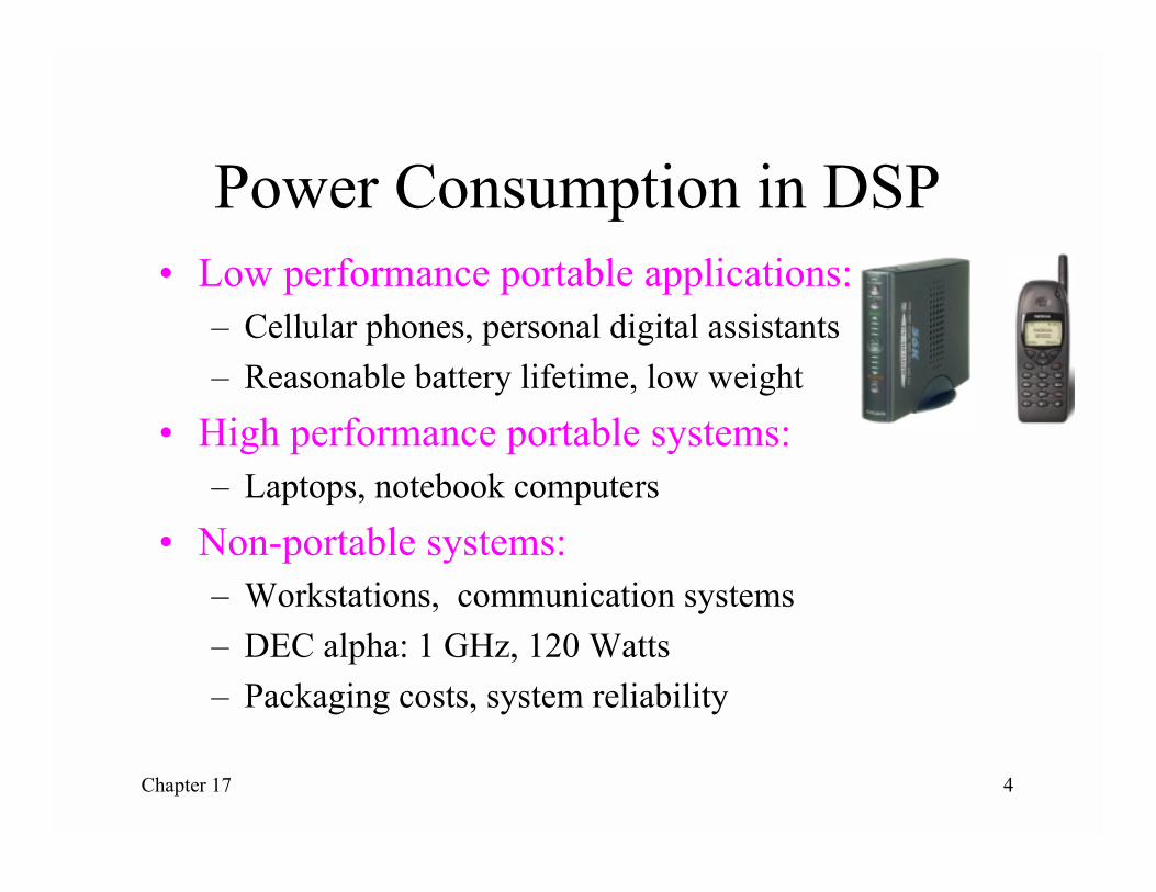
Power Consumption in DSP• Low performance portable applications:
– Cellular phones, personal digital assistants– Reasonable battery lifetime, low weight
• High performance portable systems:– Laptops, notebook computers
• Non-portable systems:– Workstations, communication systems– DEC alpha: 1 GHz, 120 Watts– Packaging costs, system reliability

Chapter 17 5
Power DissipationTwo measures are important
• Peak power (Sets dimensions)
• Average power (Battery and cooling)
dt(t)iT
VPT
0DD
DDav =
maxDDDDpeak iVP ×=

Chapter 17 6
CMOS Power Consumption
switchingforyprobabilitα
VIIVVCfα
PPPP
DDleakagescDD2DDL
leakagescdyntot
=
++=
=++=

Chapter 17 7
Dynamic Power Consumption
Energy charged in a capacitorEC = CV2/2 = CLVDD
2/2
Energy Ec is also discharged,i.e.
Etot= CL VDD2
Power consumptionP = CL VDD
2 f
Charge
VDD
Discharge

Chapter 17 8
Off-Chip Connections have High CapacitiveLoad
Reduced off Chip Data Transfers bySystem Integration
Ideally a Single Chip Solution
Reduced Power Consumption

Chapter 17 9
Switching Activity (α):Example
Pa=0.5 Px=0.25
Pd=0.5
Pb=Pc=0.5
Py=0.25
Pa=0.5 Px=0.25
Pc=0.5
Pb=0.5
Py=0.25
0.4375167Pz ==
0.37583Pz ==
Pd=0.5
Due to correlation

Chapter 17 10
Increased Switching Activity due toGlitching
Extra transitiondue to race
Dissipates energy
ab=0 zc
x
a
x
c
z
Delay in gate

Chapter 17 11
Clock Gating and Power Down
ModuleA
EnableA
CLK
ModuleB
EnableB Module
CEnableC
Only active modules should be clocked!
Controlcircuitry isneeded forclock gatingand powerdown
andNeeds wake-up

Chapter 17 12
Carry Ripple
Transitions due to carry propagation
Ci+1
Si
0
Addi Ci+4
Si+3
0
Addi+3Ci+3
Si+2
0
Addi+2Ci+2
Si+1
0
Addi+1

Chapter 17 13
BalancingOperations Example:
Addition
A HGFEDCB
S
A
H
G
F
E
D
C
B
S

Chapter 17 14
Delay as function of Supply
Chapter 17 15
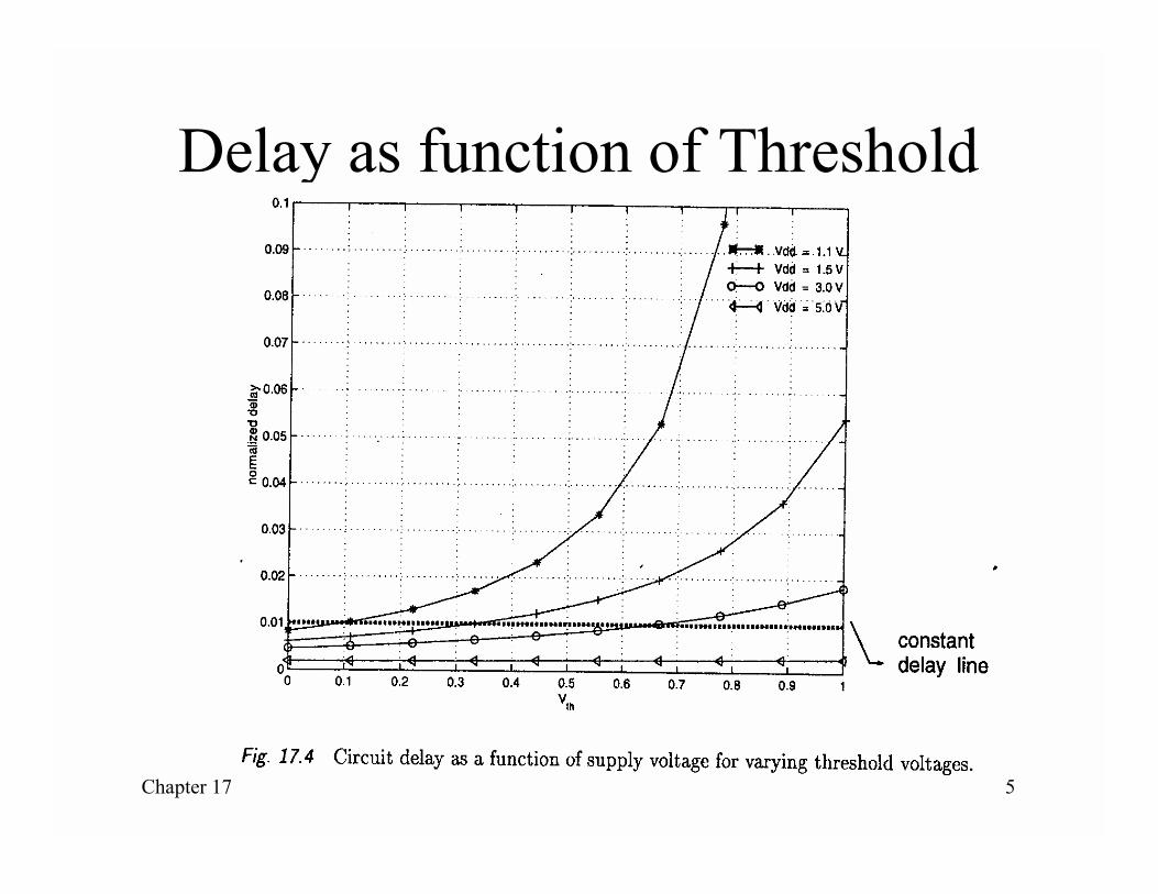
Delay as function of Threshold

Chapter 17 16
Dual VT Technology
Low VT in critical path
Reduced VDD αααα Increased delayLow VT αααα Faster but Increased Leakage

Chapter 17 17
High VT stand-byVDD
CL
standby
standby
High VT αααα low leakage
High VT αααα low leakage
Low leakage instand by whenhigh VT tansistorsturned off
Low VT
Fast
high leakage

Chapter 17 18
Low Power Gate Resizing• Systematic capture and elimination of slack using fictitious entities called Unit
Delay Fictitious Buffers.• Replace unnecessary fast gates by slower lower power gates from an
underlying gate library.• Use a simple relation between a gate’s speed and power and the UDF’s in its
fanout nets. Model the problem as an efficiently solvable ILP similar toretiming.
• In Proceedings of ARVLSI’99 Georgia Tech.
4
1
3
1
3
3
3
3
7
Critical Path = 8, UDF’s in Boxes
1
1
3
1
3
3
0
0
7
Critical Path = 8, UDF’s in Boxes
3
-3
-3
0
UDFDisplacementVariables
6

Chapter 17 19
Dual Supply Voltages for LowPower
• Components on the Critical Path exhibit no slackbut components off the critical path exhibitexcessive slack.
• A high supply voltage VDDH for critical pathcomponents and a low supply voltage VDDL fornon critical path components.
• Throughput is maintained and power consumptionis lowered.
V. Sundararajan and K.K. Parhi, "Synthesis of Low Power CMOS VLSI Circuits using Dual SupplyVoltages", Prof. of ACM\/IEEE Design Automation Conference, pp. 72-75, New Orleans, June 1999

Chapter 17 20
Dual Supply Voltages for LowPower
• Systematic capture and elimination of slack using fictitious entities called UnitDelay Fictitious Buffers.
• Switch unnecessarily fast gates to to lower supply voltage VDDL therebysaving power, critical path gates have a high supply voltage of VDDH.
• Use a simple relation between a gate’s speed/power and supply voltage withthe UDF’s in its fanout nets. Model the problem as an approximately solvableILP.
4
1
3
1
3
3
3
3
7
Critical Path = 8, UDF’s in Boxes
1
1
3
1
3
3
0
0
7
Critical Path = 8, UDF’s in Boxes
3
-3
-3
0
UDFDisplacementVariables
VDDH
VDDH
VDDH
VDDH
VDDL
VDDH
LC = Level Converter

Chapter 17 21
Dual Threshold CMOS VLSI forLow Power
• Systematic capture and elimination of slack using fictitious entities called UnitDelay Fictitious Buffers.
• Gates on the critical path have a low threshold voltage VTL and unnecessarilyfast gates are switched to a high threshold voltage VTH.
• Use a simple relation between a gate’s speed /power and threshold voltagewith the UDF’s in its fanout nets. Model the problem as an efficientlyapproximable 0-1 ILP.
4
1
3
1
3
3
3
3
7
Critical Path = 8, UDF’s in Boxes
1
1
3
1
3
3
0
0
7
Critical Path = 8, UDF’s in Boxes
3
-3
-3
0
UDFDisplacementVariables
VTL
VTL
VTL
VTLVTH
VTL
Chapter 17 22
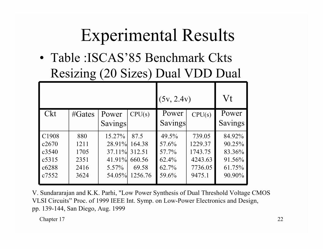
Experimental Results• Table :ISCAS’85 Benchmark Ckts
Resizing (20 Sizes) Dual VDD Dual
Ckt #Gates PowerSavings
CPU(s) PowerSavings
CPU(s) PowerSavings
C1908 880 15.27% 87.5 49.5% 739.05 84.92%c2670 1211 28.91% 164.38 57.6% 1229.37 90.25%c3540 1705 37.11% 312.51 57.7% 1743.75 83.36%c5315 2351 41.91% 660.56 62.4% 4243.63 91.56%c6288 2416 5.57% 69.58 62.7% 7736.05 61.75%c7552 3624 54.05% 1256.76 59.6% 9475.1 90.90%
Vt (5v, 2.4v)
V. Sundararajan and K.K. Parhi, "Low Power Synthesis of Dual Threshold Voltage CMOSVLSI Circuits” Proc. of 1999 IEEE Int. Symp. on Low-Power Electronics and Design, pp. 139-144, San Diego, Aug. 1999

Chapter 17 23
HEAT: Hierarchical EnergyAnalysis Tool
• Salient features:– Based on stochastic techniques– Transistor-level analysis– Effectively models glitching activity– Reasonably fast due to its hierarchical nature

Chapter 17 24
Theoretical Background
• Signal probability:– S=T / T ,where
• Transition probability:
• Conditional probability:0010
100/1
→→
→
+=
ii
i
ixx
xx pp
pp
clkgd
gdclkT :clock periodT : smallest gate delay
( )
1
)1(lim
00101101
101
=+++
+=
→→→→
=
∞→
→
iiii
i
xxxx
NS
jii
Nx
ppppNS
jxjxp
( )
10
11
1
lim
ii
i
xx
NS
ji
Nx
ppNS
jxp
−=
= =
∞→

Chapter 17 25
State Transition DiagramModeling
)()()())(1()1( 22112 nnodenxnxnxnNode ⋅⋅+−=+
)()()())(1()1( 22112 nnodenxnxnxnnode ⋅⋅+−=+
))(1())(1()1( 213 nxnxnnode −+−=+

Chapter 17 26
The HEAT algorithm
• Partitioning of systems unit into smaller sub-units• State transition diagram modeling• Edge energy computation (HSPICE)• Computation of steady-state probabilities
(MATLAB)• Edge activity computation• Computation of average energy
Energy = Wjj
⋅ EAj

Chapter 17 27
Performance Comparison
05000
1000015000200002500030000350004000045000
sec
BW4 HY4 BW8 HY8circuit
SPICEHEAT
0100020003000400050006000700080009000
uW
BW4 HY4 BW8 HY8circuit
Run-time Power
J. Satyanarayana and K.K. Parhi, "Power Estimation of Digital Datapaths using HEAT Tool",IEEE Design and Test Magazine, 17(2), pp. 101-110, April-June 2000
Chapter 17 28
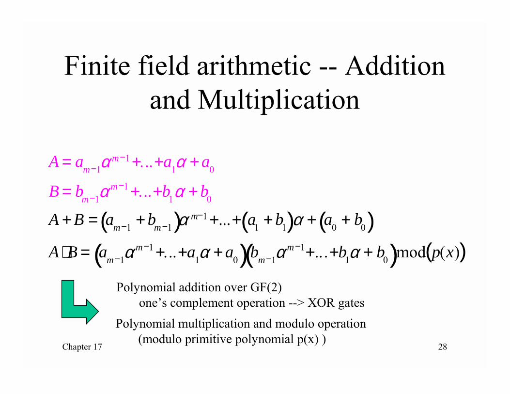
Finite field arithmetic -- Additionand Multiplication
A = am−1α m−1+...+a1α +a0
B = bm−1αm−1 +...+b1α +b0
A +B = am−1 +bm−1( )α m−1 +...+ a1 +b1( )α + a0 + b0( )A ⋅ B = am−1α
m−1 +...+a1α +a0( )bm−1αm−1+...+b1α + b0( )mod p(x)( )
Polynomial addition over GF(2) one’s complement operation --> XOR gatesPolynomial multiplication and modulo operation (modulo primitive polynomial p(x) )
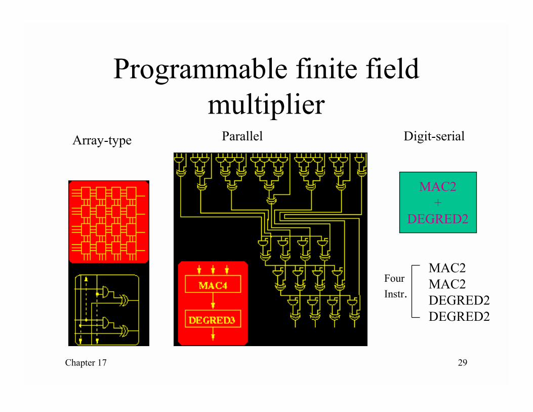
Chapter 17 29
Programmable finite fieldmultiplier
Array-type Parallel Digit-serial
MAC2MAC2DEGRED2DEGRED2
MAC2+
DEGRED2
FourInstr.
Chapter 17 30
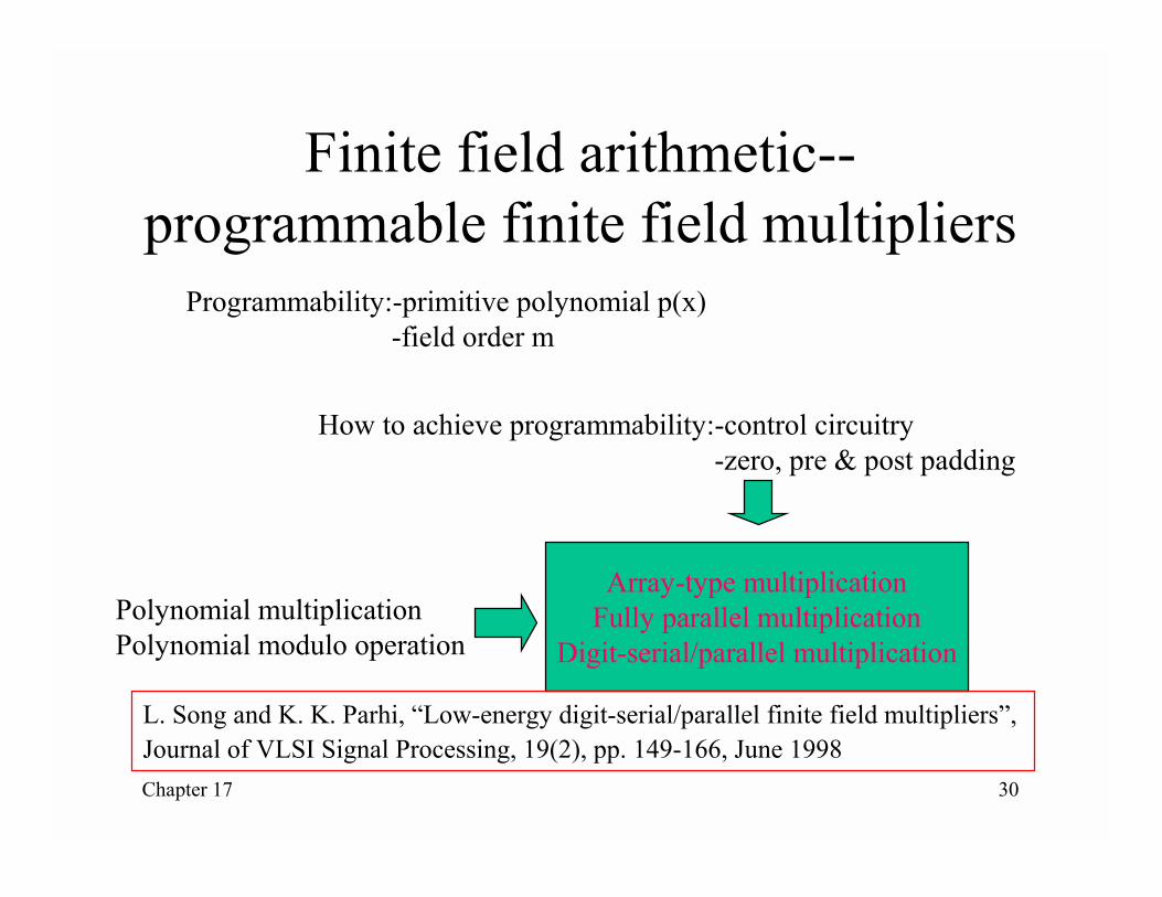
Finite field arithmetic--programmable finite field multipliers
Programmability:-primitive polynomial p(x) -field order m
How to achieve programmability:-control circuitry -zero, pre & post padding
Polynomial multiplicationPolynomial modulo operation
Array-type multiplicationFully parallel multiplication
Digit-serial/parallel multiplication
L. Song and K. K. Parhi, “Low-energy digit-serial/parallel finite field multipliers”, Journal of VLSI Signal Processing, 19(2), pp. 149-166, June 1998
Chapter 17 31
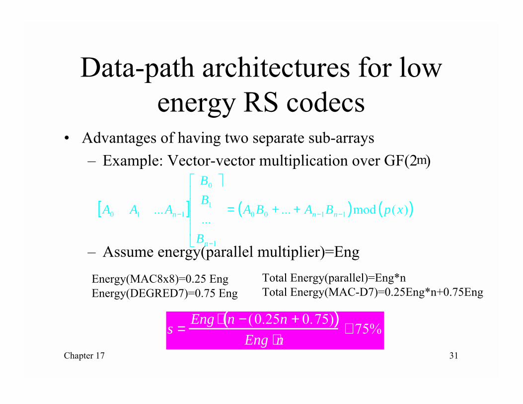
Data-path architectures for lowenergy RS codecs
• Advantages of having two separate sub-arrays– Example: Vector-vector multiplication over GF(2 )
– Assume energy(parallel multiplier)=Eng
m
[ ] ( ) ( ))(mod......
... 1100
1
1
0
110 xpBABA
B
BB
AAA nn
n
n −−
−
− ++=
�
����
�
�
Energy(MAC8x8)=0.25 EngEnergy(DEGRED7)=0.75 Eng
s =Eng ⋅ n −(0.25n + 0.75)( )
Eng ⋅n≅ 75%
Total Energy(parallel)=Eng*nTotal Energy(MAC-D7)=0.25Eng*n+0.75Eng

Chapter 17 32
Data-path architectures for low-power RS encoder
• Data-paths– One parallel finite field multiplier– Digit-serial multiplication: MACx and DEGREDy

Chapter 17 33
Data-path architectures for lowenergy RS codecs
• Data-path:– one parallel finite field multiplier– Digit-serial multiplication: MACx and DEGREDy
Energy
MAC8 + DEGRED2MAC8 + DEGRED1MAC4 + DEGRED2MAC4 + DEGRED1
Energy-delay MAC8 + DEGRED4MAC8 + DEGRED2
L. Song, K.K. Parhi, I. Kuroda, T. Nishitani, "Hardware/Software Codesign of Finite Field Datapath for Low-EnergyReed-Solomon Codecs", IEEE Trans. on VLSI Systems, 8(2), pp. 160-172, Apr. 2000
Chapter 17 34
Low power design challenges• System Integration• Application Specific architectures for
Wireless/ADSL/Security• Programmable DSPs to handle new
application requirements• Low-Power Architectures driven by
Interconnect, Crosstalk in DSM technology• How Far are we away from PDAs/Cell
Phones for wireless video, internet accessand e-commerce?


![Multicarrier Faster-than-Nyquist Signaling Transceivers · 2012. 2. 11. · viii Preface [7] D. Dasalukunte, S. Mehmood, and V. Owall, “Complexity analysis of¨ IOTA filter architectures](https://img.dokumen.tips/doc/110x75/6031a7a96cf9e618e82b5140/multicarrier-faster-than-nyquist-signaling-transceivers-2012-2-11-viii-preface.jpg)