Embed Size (px)
Citation preview

FLASH MEMORY
1
K9WAG08U1M
K9K8G08U0M K9NBG08U5M
K9XXG08UXM
* Samsung Electronics reserves the right to change products or specification without notice.
INFORMATION IN THIS DOCUMENT IS PROVIDED IN RELATION TO SAMSUNG PRODUCTS,
AND IS SUBJECT TO CHANGE WITHOUT NOTICE.
NOTHING IN THIS DOCUMENT SHALL BE CONSTRUED AS GRANTING ANY LICENSE,
EXPRESS OR IMPLIED, BY ESTOPPEL OR OTHERWISE,
TO ANY INTELLECTUAL PROPERTY RIGHTS IN SAMSUNG PRODUCTS OR TECHNOLOGY. ALL
INFORMATION IN THIS DOCUMENT IS PROVIDED
ON AS "AS IS" BASIS WITHOUT GUARANTEE OR WARRANTY OF ANY KIND.
1. For updates or additional information about Samsung products, contact your nearest Samsung office.
2. Samsung products are not intended for use in life support, critical care, medical, safety equipment, or similar
applications where Product failure could result in loss of life or personal or physical harm, or any military or
defense application, or any governmental procurement to which special terms or provisions may apply.

FLASH MEMORY
2
K9WAG08U1M
K9K8G08U0M K9NBG08U5M
Document Title
1G x 8 Bit / 2G x 8 Bit / 4G x 8 Bit NAND Flash Memory
Revision History
The attached data sheets are prepared and approved by SAMSUNG Electronics. SAMSUNG Electronics CO., LTD. reserve the right
to change the specifications. SAMSUNG Electronics will evaluate and reply to your requests and questions about device. If you have
any questions, please contact the SAMSUNG branch office near your office.
Revision No
0.0
0.1
0.2
0.3
1.0
Remark
Advance
Advance
Preliminary
Preliminary
Final
History
1. Initial issue
1. Technical note is changed
1. Icc value is changed
Draft Date
Mar. 1st. 2005
Apr. 1st. 2005
May 3rd. 2005
Sep. 26th. 2005
Nov. 4th 2005
FLASH MEMORY
3
K9WAG08U1M
K9K8G08U0M K9NBG08U5M
GENERAL DESCRIPTION
FEATURES
Voltage Supply
- 2.70V ~ 3.60V
Organization
- Memory Cell Array : (1G + 32M) x 8bit
- Data Register : (2K + 64) x 8bit
Automatic Program and Erase
- Page Program : (2K + 64)Byte
- Block Erase : (128K + 4K)Byte
Page Read Operation
- Page Size : (2K + 64)Byte
- Random Read : 20 s(Max.)
- Serial Access : 25ns(Min.)
* K9NBG08U5M : 50ns(Min.)
Fast Write Cycle Time
- Page Program time : 200 s(Typ.)
- Block Erase Time : 1.5ms(Typ.)
1G x 8 Bit / 2G x 8 Bit / 4G x 8 Bit NAND Flash Memory
Command/Address/Data Multiplexed I/O Port
Hardware Data Protection
- Program/Erase Lockout During Power Transitions
Reliable CMOS Floating-Gate Technology
- Endurance : 100K Program/Erase Cycles with 1bit/512Byte ECC)
- Data Retention : 10 Years
Command Driven Operation
Intelligent Copy-Back with internal 1bit/528Byte EDC
Unique ID for Copyright Protection
Package :
- K9K8G08U0M-YCB0/YIB0
48 - Pin TSOP I (12 x 20 / 0.5 mm pitch)
- K9K8G08U0M-PCB0/PIB0 : Pb-FREE PACKAGE
48 - Pin TSOP I (12 x 20 / 0.5 mm pitch)
- K9WAG08U1M-YCB0/YIB0
48 - Pin TSOP I (12 x 20 / 0.5 mm pitch)
- K9WAG08U1M-PCB0/PIB0 : Pb-FREE PACKAGE
48 - Pin TSOP I (12 x 20 / 0.5 mm pitch)
- K9WAG08U1M-ICB0/IIB0
52 - Pin TLGA (12 x 17 / 1.0 mm pitch)
- K9NBG08U5M-PCB0/PIB0 : Pb-FREE PACKAGE
48 - Pin TSOP I (12 x 20 / 0.5 mm pitch)
Offered in 1G x 8bit, the K9K8G08U0M is a 8G-bit NAND Flash Memory with spare 256M-bit. Its NAND cell provides the most cost-
effective solution for the solid state application market. A program operation can be performed in typical 200 s on the (2K+64)Byte
page and an erase operation can be performed in typical 1.5ms on a (128K+4K)Byte block. Data in the data register can be read out
at 25ns(K9NBG08U5M:50ns) cycle time per Byte. The I/O pins serve as the ports for address and data input/output as well as com-
mand input. The on-chip write controller automates all program and erase functions including pulse repetition, where required, and
internal verification and margining of data. Even the write-intensive systems can take advantage of the K9K8G08U0M s extended
reliability of 100K program/erase cycles by providing ECC(Error Correcting Code) with real time mapping-out algorithm. The
K9K8G08U0M is an optimum solution for large nonvolatile storage applications such as solid state file storage and other portable
applications requiring non-volatility.
An ultra high density solution having two 8Gb stacked with two chip selects is also available in standard TSOPI package and anotherultra high density solution having two 16Gb TSOPI package stacked with four chip selects is also available in TSOPI-DSP.
PRODUCT LIST
Part Number Vcc Range Organization PKG Type
K9K8G08U0M-Y,P
2.70 ~ 3.60V X8
TSOP1K9WAG08U1M-Y,P
K9WAG08U1M-I 52TLGA
K9NBG08U5M-P TSOP1-DSP

FLASH MEMORY
4
K9WAG08U1M
K9K8G08U0M K9NBG08U5M
PIN CONFIGURATION (TSOP1)
K9K8G08U0M-YCB0,PCB0/YIB0,PIB0
PACKAGE DIMENSIONS
48-PIN LEAD/LEAD FREE PLASTIC THIN SMALL OUT-LINE PACKAGE TYPE(I)
48 - TSOP1 - 1220F Unit :mm/Inch
0.787 0.008
20.00 0.20
#1
#24
0.2
0+
0.0
7-0
.03
0.0
08
+0.0
03
-0.0
01
0.5
00
.01
97
#48
#25
0.4
88
12.4
0M
AX
12.0
00
.47
2
0.1
0
0.0
04 M
AX
0.2
50
.01
0(
)
0.039 0.002
1.00 0.05
0.0020.05
MIN
0.0471.20
MAX
0.45~0.750.018~0.030
0.724 0.004
18.40 0.10
0~8
0.0
10
0.2
5T
YP
0.1
25
+0.0
75
0.0
35
0.0
05
+0.0
03
-0.0
01
0.500.020
( )
48-pin TSOP1
Standard Type
12mm x 20mm
123456789
101112131415161718192021222324
484746454443424140393837363534333231302928272625
N.CN.CN.CN.CN.CN.CR/B RECE
N.CN.CVccVssN.CN.CCLEALEWEWPN.CN.CN.CN.CN.C
N.CN.CN.CN.CI/O7I/O6I/O5I/O4N.CN.CN.CVccVssN.CN.CN.CI/O3I/O2I/O1I/O0N.CN.CN.CN.C

FLASH MEMORY
5
K9WAG08U1M
K9K8G08U0M K9NBG08U5M
PIN CONFIGURATION (TSOP1)
K9WAG08U1M-YCB0,PCB0/YIB0,PIB0
PACKAGE DIMENSIONS
48-PIN LEAD/LEAD FREE PLASTIC THIN SMALL OUT-LINE PACKAGE TYPE(I)
48 - TSOP1 - 1220F Unit :mm/Inch
0.787 0.008
20.00 0.20
#1
#24
0.2
0+
0.0
7-0
.03
0.0
08
+0.0
03
-0.0
01
0.5
00
.01
97
#48
#25
0.4
88
12.4
0M
AX
12.0
00
.47
2
0.1
0
0.0
04 M
AX
0.2
50
.01
0(
)
0.039 0.002
1.00 0.05
0.0020.05
MIN
0.0471.20
MAX
0.45~0.750.018~0.030
0.724 0.004
18.40 0.10
0~8
0.0
10
0.2
5T
YP
0.1
25
+0.0
75
0.0
35
0.0
05
+0.0
03
-0.0
01
0.500.020
( )
48-pin TSOP1
Standard Type
12mm x 20mm
123456789
101112131415161718192021222324
484746454443424140393837363534333231302928272625
N.CN.CN.CN.CN.C
R/B2 R/B1
RECE1CE2N.CVccVssN.CN.CCLEALEWEWPN.CN.CN.CN.CN.C
N.CN.CN.CN.CI/O7I/O6I/O5I/O4N.CN.CN.CVccVssN.CN.CN.CI/O3I/O2I/O1I/O0N.CN.CN.CN.C
FLASH MEMORY
6
K9WAG08U1M
K9K8G08U0M K9NBG08U5M
1.00
1.001.00
1.00
2.00
7 6 5 4 3 2 1
1.0
0
1.0
01
.00
12.00 0.10
#A1
17
.00
0.1
0
17.0
00
.10
B
A12.00 0.10
(Datum B)
(Datum A)
12
.00
10.00
2.5
02
.50
2.0
0
0.5
01.3
0
A
B
C
D
E
F
G
H
J
K
L
M
N
12- 1.00 0.05 41- 0.70 0.05
Side View
1.0
Max
0.10 C
17.00 0.10
Top View Bottom View
A B C D E F G H J K L M N
7
6
5
4
3
2
1
K9WAG08U1M - ICB0 / IIB0
52-TLGA (measured in millimeters)
NC NC NC NC NC NC
NC NC NCNCNCNC
NC
NCNC
NC
VccVcc
Vss
Vss
Vss
/RE1
/RE2
/CE1 /CE2
CLE1CLE2
ALE1
ALE2
/WE1
/WE2
/WP1
/WP2R/B1
R/B2
Vss
IO0-1
IO0-2
IO1-1
IO1-2
IO2-1
IO3-1
IO2-2
IO3-2
IO4-1 IO4-2
IO5-1
IO5-2
IO6-1
IO6-2
IO7-1
IO7-2
ABCM0.1 ABCM0.1
PACKAGE DIMENSIONS

FLASH MEMORY
7
K9WAG08U1M
K9K8G08U0M K9NBG08U5M
18.80 MAX REF
12
.40
MA
X R
EF
0.1
3~
0.2
3
Pin #1
#1
#24
#48
0.5
0 T
YP
#25
(0.1
0)
A
(0.2
49)
BA
SIC
GA
GE
PL
AN
E
0.399~0.60020.00 0.20
0.0
2 M
IN
2.3
5 M
AX
TY
P B
OT
H S
IDE
SB
OT
TO
M T
SO
P O
NLY
(0.1
0)
A
-A-
SEATING
PIN CONFIGURATION (TSOP1-DSP)
K9NBG08U5M-PCB0/PIB0
PACKAGE DIMENSIONS
48-PIN LEAD FREE PLASTIC THIN SMALL OUT-LINE PACKAGE TYPE(I)
48 - TSOP1 - 1220AF Unit :mm/Inch
PLANE
123456789
101112131415161718192021222324
484746454443424140393837363534333231302928272625
48-pin TSOP1
Dual Stacked Package
12mm x 20mm
N.CN.CN.C
R/B2R/B1 RECE1CE2N.CVccVss
CLEALEWEWPN.CN.CN.CN.CN.C
N.CN.CN.CN.CI/O7I/O6I/O5I/O4N.CN.C
VccVssN.CN.CN.CI/O3I/O2I/O1I/O0N.CN.CN.CN.C
N.C
R/B4R/B3
CE3CE4

FLASH MEMORY
8
K9WAG08U1M
K9K8G08U0M K9NBG08U5M
PIN DESCRIPTION
NOTE : Connect all VCC and VSS pins of each device to common power supply outputs.
Do not leave VCC or VSS disconnected.
There are two CE pins (CE1 & CE2) in the K9WAG08U1M and four CE pins (CE1 & CE2 & CE3 & CE4) in the K9NBG08U5M. There are two R/B pins (R/B1 & R/B2) in the K9WAG08U1M and four R/B pins (R/B1 & R/B2 & R/B3 & R/B4) in the K9NBG08U5M.
Pin Name Pin Function
I/O0 ~ I/O7
DATA INPUTS/OUTPUTS
The I/O pins are used to input command, address and data, and to output data during read operations. The I/
O pins float to high-z when the chip is deselected or when the outputs are disabled.
CLE
COMMAND LATCH ENABLE
The CLE input controls the activating path for commands sent to the command register. When active high,
commands are latched into the command register through the I/O ports on the rising edge of the WE signal.
ALE
ADDRESS LATCH ENABLE
The ALE input controls the activating path for address to the internal address registers. Addresses are
latched on the rising edge of WE with ALE high.
CE / CE1
CHIP ENABLE
The CE / CE1 input is the device selection control. When the device is in the Busy state, CE / CE1 high is
ignored, and the device does not return to standby mode in program or erase operation.
Regarding CE / CE1 control during read operation , refer to ’Page Read’ section of Device operation.
CE2CHIP ENABLE
The CE2 input enables the second K9K8G08U0M
RE
READ ENABLE
The RE input is the serial data-out control, and when active drives the data onto the I/O bus. Data is valid
tREA after the falling edge of RE which also increments the internal column address counter by one.
WE
WRITE ENABLE
The WE input controls writes to the I/O port. Commands, address and data are latched on the rising edge of
the WE pulse.
WP
WRITE PROTECT
The WP pin provides inadvertent program/erase protection during power transitions. The internal high volt-
age generator is reset when the WP pin is active low.
R/B / R/B1
READY/BUSY OUTPUT
The R/B / R/B1 output indicates the status of the device operation. When low, it indicates that a program,
erase or random read operation is in process and returns to high state upon completion. It is an open drain
output and does not float to high-z condition when the chip is deselected or when outputs are disabled.
VccPOWER
VCC is the power supply for device.
Vss GROUND
N.CNO CONNECTION
Lead is not internally connected.

FLASH MEMORY
9
K9WAG08U1M
K9K8G08U0M K9NBG08U5M
2K Bytes 64 Bytes
Figure 1. K9K8G08U0M Functional Block Diagram
Figure 2. K9K8G08U0M Array Organization
NOTE : Column Address : Starting Address of the Register.
* L must be set to "Low".
* The device ignores any additional input of address cycles than required.
I/O 0 I/O 1 I/O 2 I/O 3 I/O 4 I/O 5 I/O 6 I/O 7
1st Cycle A0 A1 A2 A3 A4 A5 A6 A7
2nd Cycle A8 A9 A10 A11 *L *L *L *L
3rd Cycle A12 A13 A14 A15 A16 A17 A18 A19
4th Cycle A20 A21 A22 A23 A24 A25 A26 A27
5th Cycle A28 A29 A30 *L *L *L *L *L
VCC
X-Buffers
Command
I/O Buffers & Latches
Latches& Decoders
Y-BuffersLatches& Decoders
Register
Control Logic& High Voltage
Generator Global Buffers OutputDriver
VSS
A12 - A30
A0 - A11
Command
CEREWE
CLE WP
I/0 0
I/0 7
VCC
VSS
512K Pages
(=8,192 Blocks)
2K Bytes
8 bit
64 Bytes
1 Block = 64 Pages
(128K + 4k) Byte
I/O 0 ~ I/O 7
1 Page = (2K + 64)Bytes
1 Block = (2K + 64)B x 64 Pages
= (128K + 4K) Bytes
1 Device = (2K+64)B x 64Pages x 8,192 Blocks
= 8,448 Mbits
Row Address
Page Register
ALE
8,192M + 256M BitNAND Flash
ARRAY
(2,048 + 64)Byte x 524,288
Y-Gating
Row Address
Column Address
Column Address
Row Address
Data Register & S/A

FLASH MEMORY
10
K9WAG08U1M
K9K8G08U0M K9NBG08U5M
Product IntroductionThe K9K8G08U0M is a 8,448Mbit(8,858,370,048 bit) memory organized as 524,288 rows(pages) by 2,112x8 columns. Spare 64x8
columns are located from column address of 2,048~2,111. A 2,112-byte data register is connected to memory cell arrays accommo-
dating data transfer between the I/O buffers and memory during page read and page program operations. The memory array is made
up of 32 cells that are serially connected to form a NAND structure. Each of the 32 cells resides in a different page. A block consists
of two NAND structured strings. A NAND structure consists of 32 cells. Total 1,081,344 NAND cells reside in a block. The program
and read operations are executed on a page basis, while the erase operation is executed on a block basis. The memory array con-
sists of 8,192 separately erasable 128K-byte blocks. It indicates that the bit by bit erase operation is prohibited on the K9K8G08U0M.
The K9K8G08U0M has addresses multiplexed into 8 I/Os. This scheme dramatically reduces pin counts and allows system upgrades
to future densities by maintaining consistency in system board design. Command, address and data are all written through I/O's by
bringing WE to low while CE is low. Those are latched on the rising edge of WE. Command Latch Enable(CLE) and Address Latch
Enable(ALE) are used to multiplex command and address respectively, via the I/O pins. Some commands require one bus cycle. For
example, Reset Command, Status Read Command, etc require just one cycle bus. Some other commands, like page read and block
erase and page program, require two cycles: one cycle for setup and the other cycle for execution. The 1056M byte physical space
requires 31 addresses, thereby requiring five cycles for addressing : 2 cycles of column address, 3 cycles of row address, in that
order. Page Read and Page Program need the same five address cycles following the required command input. In Block Erase oper-
ation, however, only the three row address cycles are used. Device operations are selected by writing specific commands into the
command register. Table 1 defines the specific commands of the K9K8G08U0M.
In addition to the enhanced architecture and interface, the device incorporates copy-back program feature from one page to another
page without need for transporting the data to and from the external buffer memory. Since the time-consuming serial access and
data-input cycles are removed, system performance for solid-state disk application is significantly increased.
The K9WAG08U1M is composed of two K9K8G08U0M chips which are selected separately by each CE1 and CE2 and theK9NBG08U5M is composed of four K9K8G08U0M chips which are selected seperately by each CE1, CE2, CE3 and CE4. Therefore,in terms of each CE, the basic operations of K9WAG08U0M and K9NBG08U5M are same with K9K8G08U0M except some AC/DCcharateristics.
Table 1. Command Sets
NOTE : 1. Random Data Input/Output can be executed in a page.
2. Read EDC Status is only available on Copy Back operation.
3. Interleave-operation between two chips is allowed.
It’s prohibited to use F1h and F2h commands for other operations except interleave-operation.
4. Any command between 11h and 81h is prohibited except 70h, F1h, F2h and FFh .
Caution : Any undefined command inputs are prohibited except for above command set of Table 1.
Function 1st Cycle 2nd Cycle Acceptable Command during Busy
Read 00h 30h
Read for Copy Back 00h 35h
Read ID 90h -
Reset FFh - O
Page Program 80h 10h
Two-Plane Page Program(4) 80h---11h 81h---10h
Copy-Back Program 85h 10h
Two-Plane Copy-Back Program(4) 85h---11h 81h---10h
Block Erase 60h D0h
Two-Plane Block Erase 60h---60h D0h
Random Data Input(1) 85h -
Random Data Output(1) 05h E0h
Read Status 70h O
Read EDC Status(2) 7Bh O
Chip1 Status(3) F1h O
Chip2 Status(3) F2h O

FLASH MEMORY
11
K9WAG08U1M
K9K8G08U0M K9NBG08U5M
K9K8G08U0M is arranged in four 2Gb memory planes. Each plane contains 2,048 blocks and 2112 byte page registers. This allows it
to perform simultaneous page program and block erase by selecting one page or block from each plane. The block address map is
configured so that two-plane program/erase operations can be executed by dividing the memory array into plane 0~1 or plane 2~3
separately.
For example, two-plane program/erase operation into plane 0 and plane 2 is prohibited. That is to say, two-plane program/erase oper-
ation into plane 0 and plane 1 or into plane 2 and plane 3 is allowed
Plane 0 Plane 1 Plane 2 Plane 3
(2048 Block) (2048 Block) (2048 Block) (2048 Block)
Page 0
Page 1
Page 63
Page 62
Memory Map
Block 0
Page 0
Page 1
Page 63
Page 62
Block 1
Page 0
Page 1
Page 63
Page 62
Block 4096
Page 0
Page 1
Page 63
Page 62
Block 4097
Page 0
Page 1
Page 63
Page 62
Block 4094
Page 0
Page 1
Page 63
Page 62
Block 4095
Page 0
Page 1
Page 63
Page 62
Block 8190
Page 0
Page 1
Page 63
Page 62
Block 8191
2112byte Page Registers 2112byte Page Registers 2112byte Page Registers 2112byte Page Registers
Page 0
Page 1
Page 63
Page 62
Block 2
Page 0
Page 1
Page 63
Page 62
Block 3
Page 0
Page 1
Page 63
Page 62
Block 4098
Page 0
Page 1
Page 63
Page 62
Block 4099
Page 0
Page 1
Page 63
Page 62
Block 4092
Page 0
Page 1
Page 63
Page 62
Block 4093
Page 0
Page 1
Page 63
Page 62
Block 8188
Page 0
Page 1
Page 63
Page 62
Block 8189

FLASH MEMORY
12
K9WAG08U1M
K9K8G08U0M K9NBG08U5M
DC AND OPERATING CHARACTERISTICS(Recommended operating conditions otherwise noted.)
NOTE : 1. VIL can undershoot to -0.4V and VIH can overshoot to VCC +0.4V for durations of 20 ns or less. 2. Typical value is measured at Vcc=3.3V, TA=25 C. Not 100% tested.
3. The typical value of the K9WAG08U1M’s ISB2 is 40 A and the maximum value is 200 A. 4. The typical value of the K9NBG08U5M’s ISB2 is 80 A and the maximum value is 400 A. 5. The maximum value of K9WAG08U1M-Y,P’s ILI and ILO is ±40 A the maximum value of K9WAG08U1M-I’s ILI and ILO is ±20 A 6. The maximum value of K9NBG08U5M’s ILI and ILO is A.
Parameter Symbol Test Conditions Min Typ Max Unit
Operating
Current
Page Read with
Serial AccessICC1
tRC=25ns (K9NBG08U5M: 50ns)
CE=VIL, IOUT=0mA- 25 35
mAProgram ICC2 -
Erase ICC3 -
Stand-by Current(TTL) ISB1 CE=VIH, WP=0V/VCC - - 1
Stand-by Current(CMOS) ISB2 CE=VCC-0.2, WP=0V/VCC - 20 100
AInput Leakage Current ILI VIN=0 to Vcc(max) - - ±20
Output Leakage Current ILO VOUT=0 to Vcc(max) - - ±20
Input High Voltage VIH(1) - 0.8xVcc - Vcc+0.3
VInput Low Voltage, All inputs VIL(1) - -0.3 - 0.2xVcc
Output High Voltage Level VOH IOH=-400 A 2.4 - -
Output Low Voltage Level VOL IOL=2.1mA - - 0.4
Output Low Current(R/B) IOL(R/B) VOL=0.4V 8 10 - mA
RECOMMENDED OPERATING CONDITIONS(Voltage reference to GND, K9XXG08UXM-XCB0 :TA=0 to 70 C, K9XXG08UXM-XIB0:TA=-40 to 85 C)
Parameter Symbol Min Typ. Max Unit
Supply Voltage VCC 2.7 3.3 3.6 V
Supply Voltage VSS 0 0 0 V
ABSOLUTE MAXIMUM RATINGS
NOTE : 1. Minimum DC voltage is -0.6V on input/output pins. During transitions, this level may undershoot to -2.0V for periods <30ns. Maximum DC voltage on input/output pins is VCC+0.3V which, during transitions, may overshoot to VCC+2.0V for periods <20ns.
2. Permanent device damage may occur if ABSOLUTE MAXIMUM RATINGS are exceeded. Functional operation should be restricted to the conditions as detailed in the operational sections of this data sheet. Exposure to absolute maximum rating conditions for extended periods may affect reliability.
Parameter Symbol Rating Unit
Voltage on any pin relative to VSS
VCC -0.6 to +4.6
VVIN -0.6 to +4.6
VI/O -0.6 to Vcc+0.3 (<4.6V)
Temperature Under BiasK9XXG08UXM-XCB0
TBIAS-10 to +125
CK9XXG08UXM-XIB0 -40 to +125
Storage TemperatureK9XXG08UXM-XCB0
TSTG -65 to +150 CK9XXG08UXM-XIB0
Short Circuit Current IOS 5 mA
FLASH MEMORY
13
K9WAG08U1M
K9K8G08U0M K9NBG08U5M
CAPACITANCE(TA=25 C, VCC=3.3V, f=1.0MHz)
NOTE : Capacitance is periodically sampled and not 100% tested. K9WAG08U1M-IXB0’s capacitance(I/O, Input) is 20pF.
Item SymbolTest
ConditionMin
MaxUnit
K9K8G08U0M K9WAG08U1M* K9NBG08U5M
Input/Output Capacitance CI/O VIL=0V - 20 40 80 pF
Input Capacitance CIN VIN=0V - 20 40 80 pF
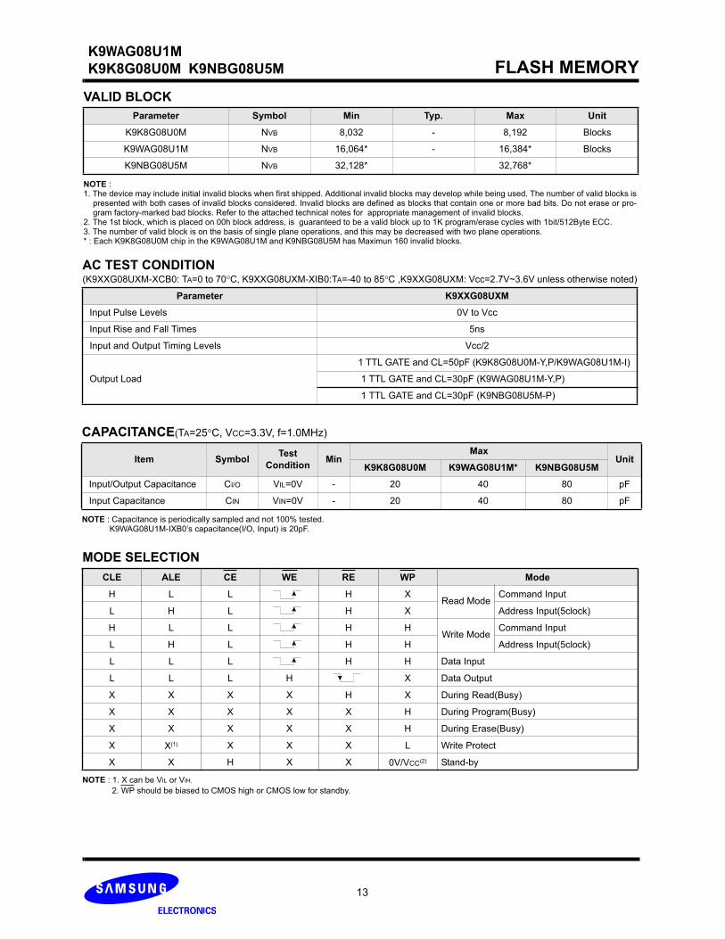
VALID BLOCK
NOTE : 1. The device may include initial invalid blocks when first shipped. Additional invalid blocks may develop while being used. The number of valid blocks is
presented with both cases of invalid blocks considered. Invalid blocks are defined as blocks that contain one or more bad bits. Do not erase or pro-gram factory-marked bad blocks. Refer to the attached technical notes for appropriate management of invalid blocks.
2. The 1st block, which is placed on 00h block address, is guaranteed to be a valid block up to 1K program/erase cycles with 1bit/512Byte ECC.3. The number of valid block is on the basis of single plane operations, and this may be decreased with two plane operations.* : Each K9K8G08U0M chip in the K9WAG08U1M and K9NBG08U5M has Maximun 160 invalid blocks.
Parameter Symbol Min Typ. Max Unit
K9K8G08U0M NVB 8,032 - 8,192 Blocks
K9WAG08U1M NVB 16,064* - 16,384* Blocks
K9NBG08U5M NVB 32,128* 32,768*
AC TEST CONDITION(K9XXG08UXM-XCB0: TA=0 to 70 C, K9XXG08UXM-XIB0:TA=-40 to 85 C ,K9XXG08UXM: Vcc=2.7V~3.6V unless otherwise noted)
Parameter K9XXG08UXM
Input Pulse Levels 0V to Vcc
Input Rise and Fall Times 5ns
Input and Output Timing Levels Vcc/2
Output Load
1 TTL GATE and CL=50pF (K9K8G08U0M-Y,P/K9WAG08U1M-I)
1 TTL GATE and CL=30pF (K9WAG08U1M-Y,P)
1 TTL GATE and CL=30pF (K9NBG08U5M-P)
MODE SELECTION
NOTE : 1. X can be VIL or VIH.
2. WP should be biased to CMOS high or CMOS low for standby.
CLE ALE CE WE RE WP Mode
H L L H XRead Mode
Command Input
L H L H X Address Input(5clock)
H L L H HWrite Mode
Command Input
L H L H H Address Input(5clock)
L L L H H Data Input
L L L H X Data Output
X X X X H X During Read(Busy)
X X X X X H During Program(Busy)
X X X X X H During Erase(Busy)
X X(1) X X X L Write Protect
X X H X X 0V/VCC(2) Stand-by

FLASH MEMORY
14
K9WAG08U1M
K9K8G08U0M K9NBG08U5M
AC Timing Characteristics for Command / Address / Data Input
NOTES : 1. The transition of the corresponding control pins must occur only once while WE is held low 2. tADL is the time from the WE rising edge of final address cycle to the WE rising edge of first data cycle
Parameter Symbol
Min Max
UnitK9NBG08U5M
K9K8G08U0MK9NBG08U5M
K9K8G08U0M
K9WAG08U1M K9WAG08U1M
CLE Setup Time tCLS(1) 25 12 - - ns
CLE Hold Time tCLH 10 5 - - ns
CE Setup Time tCS(1) 35 20 - - ns
CE Hold Time tCH 10 5 - - ns
WE Pulse Width tWP 25 12 - - ns
ALE Setup Time tALS(1) 25 12 - - ns
ALE Hold Time tALH 10 5 - - ns
Data Setup Time tDS(1) 20 12 - - ns
Data Hold Time tDH 10 5 - - ns
Write Cycle Time tWC 45 25 - - ns
WE High Hold Time tWH 15 10 - - ns
Address to Data Loading Time tADL(2) 70 70 - - ns
Program / Erase Characteristics
NOTE 1. Typical value is measured at Vcc=3.3V, TA=25 C. Not 100% tested.
2. Typical program time is defined as the time within which more than 50% of the whole pages are programmed at 3.3V Vcc and 25 C temperature.
Parameter Symbol Min Typ Max Unit
Program Time tPROG - 200 700 s
Dummy Busy Time for Two-Plane Page Program tDBSY - 0.5 1 s
Number of Partial Program Cycles Nop - - 4 cycles
Block Erase Time tBERS - 1.5 2 ms

FLASH MEMORY
15
K9WAG08U1M
K9K8G08U0M K9NBG08U5M
AC Characteristics for Operation
NOTE: 1. If reset command(FFh) is written at Ready state, the device goes into Busy for maximum 5 s.
Parameter Symbol
Min Max
UnitK9NBG08U5M
K9K8G08U0MK9NBG08U5M
K9K8G08U0M
K9WAG08U1 K9WAG08U1
Data Transfer from Cell to Register tR - 20 20 s
ALE to RE Delay tAR 10 10 - ns
CLE to RE Delay tCLR 10 10 - ns
Ready to RE Low tRR 20 20 - ns
RE Pulse Width tRP 25 12 - ns
WE High to Busy tWB - - 100 100 ns
Read Cycle Time tRC 50 25 - - ns
RE Access Time tREA - - 30 20 ns
CE Access Time tCEA - - 45 25 ns
RE High to Output Hi-Z tRHZ - - 100 100 ns
CE High to Output Hi-Z tCHZ - - 30 30 ns
RE High to Output hold tRHOH 15 15 - - ns
RE Low to Output hold tRLOH - 5 - - ns
CE High to Output hold tCOH 15 15 - - ns
RE High Hold Time tREH 15 10 - - ns
Output Hi-Z to RE Low tIR 0 0 - - ns
RE High to WE Low tRHW 100 100 - - ns
WE High to RE Low tWHR 60 60 - - ns
Device Resetting Time(Read/Program/Erase) tRST - - 5/10/500(1) 5/10/500(1) s
FLASH MEMORY
16
K9WAG08U1M
K9K8G08U0M K9NBG08U5M
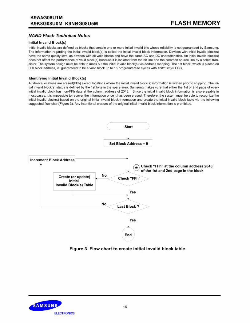
NAND Flash Technical Notes
Identifying Initial Invalid Block(s)
Initial Invalid Block(s)
Initial invalid blocks are defined as blocks that contain one or more initial invalid bits whose reliability is not guaranteed by Samsung.
The information regarding the initial invalid block(s) is called the initial invalid block information. Devices with initial invalid block(s)
have the same quality level as devices with all valid blocks and have the same AC and DC characteristics. An initial invalid block(s)
does not affect the performance of valid block(s) because it is isolated from the bit line and the common source line by a select tran-
sistor. The system design must be able to mask out the initial invalid block(s) via address mapping. The 1st block, which is placed on
00h block address, is guaranteed to be a valid block up to 1K program/erase cycles with 1bit/512Byte ECC.
All device locations are erased(FFh) except locations where the initial invalid block(s) information is written prior to shipping. The ini-
tial invalid block(s) status is defined by the 1st byte in the spare area. Samsung makes sure that either the 1st or 2nd page of every
initial invalid block has non-FFh data at the column address of 2048. Since the initial invalid block information is also erasable in
most cases, it is impossible to recover the information once it has been erased. Therefore, the system must be able to recognize the
initial invalid block(s) based on the original initial invalid block information and create the initial invalid block table via the following
suggested flow chart(Figure 3). Any intentional erasure of the original initial invalid block information is prohibited.
*Check "FFh" at the column address 2048
Figure 3. Flow chart to create initial invalid block table.
Start
Set Block Address = 0
Check "FFh"
Increment Block Address
Last Block ?
End
No
Yes
Yes
Create (or update) No
Initial
of the 1st and 2nd page in the block
Invalid Block(s) Table

FLASH MEMORY
17
K9WAG08U1M
K9K8G08U0M K9NBG08U5M
NAND Flash Technical Notes (Continued)
Program Flow Chart
Start
I/O 6 = 1 ?
I/O 0 = 0 ? No*
Write 80h
Write Address
Write Data
Write 10h
Read Status Register
Program Completed
or R/B = 1 ?
Program Error
Yes
No
Yes
: If program operation results in an error, map out the block including the page in error and copy the
target data to another block.
*
Error in write or read operation
Within its life time, additional invalid blocks may develop with NAND Flash memory. Refer to the qualification report for the actual
data.The following possible failure modes should be considered to implement a highly reliable system. In the case of status read fail-
ure after erase or program, block replacement should be done. Because program status fail during a page program does not affect
the data of the other pages in the same block, block replacement can be executed with a page-sized buffer by finding an erased
empty block and reprogramming the current target data and copying the rest of the replaced block. In case of Read, ECC must be
employed. To improve the efficiency of memory space, it is recommended that the read or verification failure due to single bit error be
reclaimed by ECC without any block replacement. The said additional block failure rate does not include those reclaimed blocks.
Failure Mode Detection and Countermeasure sequence
Write Erase Failure Status Read after Erase --> Block Replacement
Program Failure Status Read after Program --> Block Replacement
Read Single Bit Failure Verify ECC -> ECC Correction
ECC : Error Correcting Code --> Hamming Code etc.
Example) 1bit correction & 2bit detection
FLASH MEMORY
18
K9WAG08U1M
K9K8G08U0M K9NBG08U5M
Erase Flow Chart
Start
I/O 6 = 1 ?
I/O 0 = 0 ? No*
Write 60h
Write Block Address
Write D0h
Read Status Register
or R/B = 1 ?
Erase Error
Yes
No
: If erase operation results in an error, map out
the failing block and replace it with another block. *
Erase Completed
Yes
Read Flow Chart
Start
Verify ECC No
Write 00h
Write Address
Read Data
ECC Generation
Reclaim the Error
Page Read Completed
Yes
NAND Flash Technical Notes (Continued)
Write 30h
Block Replacement
* Step1
When an error happens in the nth page of the Block ’A’ during erase or program operation.
* Step2
Copy the data in the 1st ~ (n-1)th page to the same location of another free block. (Block ’B’)
* Step3
Then, copy the nth page data of the Block ’A’ in the buffer memory to the nth page of the Block ’B’.
* Step4
Do not erase or program to Block ’A’ by creating an ’invalid Block’ table or other appropriate scheme.
Buffer memory of the controller.
1st
Block A
Block B
(n-1)th
nth
(page)
1st
(n-1)th
nth
(page)
an error occurs.1
2
FLASH MEMORY
19
K9WAG08U1M
K9K8G08U0M K9NBG08U5M
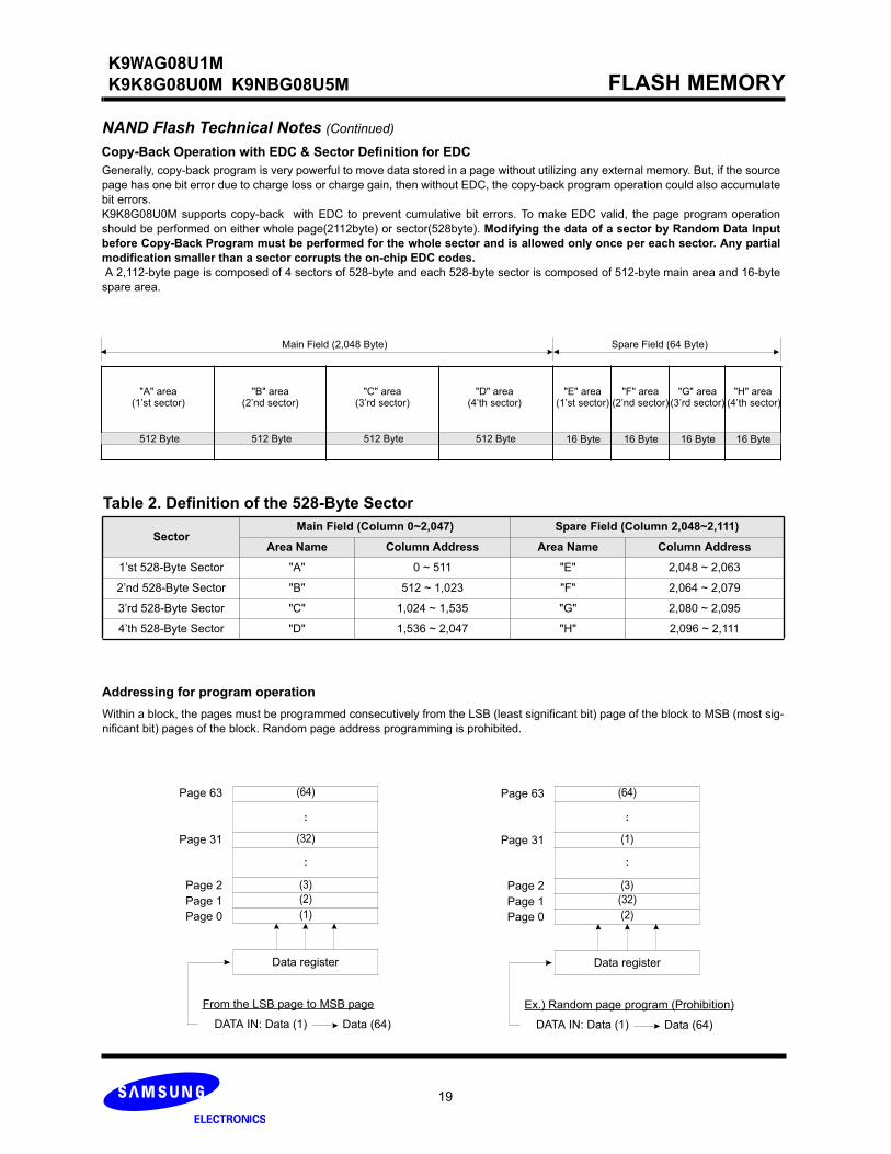
NAND Flash Technical Notes (Continued)
Copy-Back Operation with EDC & Sector Definition for EDC
Generally, copy-back program is very powerful to move data stored in a page without utilizing any external memory. But, if the source
page has one bit error due to charge loss or charge gain, then without EDC, the copy-back program operation could also accumulate
bit errors.
K9K8G08U0M supports copy-back with EDC to prevent cumulative bit errors. To make EDC valid, the page program operation
should be performed on either whole page(2112byte) or sector(528byte). Modifying the data of a sector by Random Data Input
before Copy-Back Program must be performed for the whole sector and is allowed only once per each sector. Any partial
modification smaller than a sector corrupts the on-chip EDC codes.
A 2,112-byte page is composed of 4 sectors of 528-byte and each 528-byte sector is composed of 512-byte main area and 16-byte
spare area.
"A" area
512 Byte
(1’st sector)"H" area
(4’th sector)
Main Field (2,048 Byte)
16 Byte
"G" area(3’rd sector)
16 Byte
"F" area(2’nd sector)
16 Byte
"E" area(1’st sector)
16 Byte
"B" area
512 Byte
(2’nd sector)"C" area
512 Byte
(3’rd sector)"D" area
512 Byte
(4’th sector)
Spare Field (64 Byte)
Table 2. Definition of the 528-Byte Sector
SectorMain Field (Column 0~2,047) Spare Field (Column 2,048~2,111)
Area Name Column Address Area Name Column Address
1’st 528-Byte Sector "A" 0 ~ 511 "E" 2,048 ~ 2,063
2’nd 528-Byte Sector "B" 512 ~ 1,023 "F" 2,064 ~ 2,079
3’rd 528-Byte Sector "C" 1,024 ~ 1,535 "G" 2,080 ~ 2,095
4’th 528-Byte Sector "D" 1,536 ~ 2,047 "H" 2,096 ~ 2,111
Within a block, the pages must be programmed consecutively from the LSB (least significant bit) page of the block to MSB (most sig-
nificant bit) pages of the block. Random page address programming is prohibited.
From the LSB page to MSB page
DATA IN: Data (1) Data (64)
(1)
(2)
(3)
(32)
(64)
Data register
Page 0
Page 1
Page 2
Page 31
Page 63
Ex.) Random page program (Prohibition)
DATA IN: Data (1) Data (64)
(2)
(32)
(3)
(1)
(64)
Data register
Page 0
Page 1
Page 2
Page 31
Page 63
Addressing for program operation
:
:
:
:

FLASH MEMORY
20
K9WAG08U1M
K9K8G08U0M K9NBG08U5M
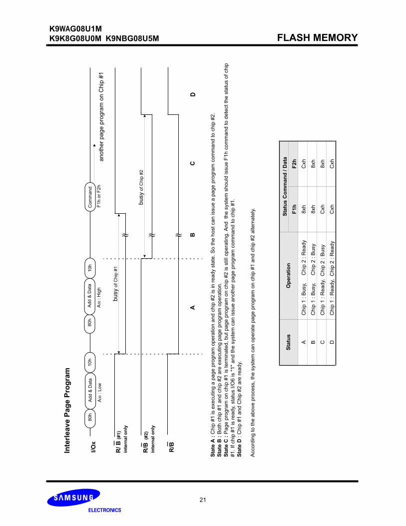
Interleave Page Program
K9K8G08U0M is composed of two K9F4G08U0Ms. K9K8G08U0M provides interleaving operation between two K9F4G08U0Ms.
This interleaving page program improves the system throughput almost twice compared to non-interleaving page program.
At first, the host issues page program command to one of the K9F4G08U0M chips, say K9F4G08U0M(chip #1). Due to this
K9K8G08U0M goes into busy state. During this time, K9F4G08U0M(chip #2) is in ready state. So it can execute the page program
command issued by the host.
After the execution of page program by K9F4G08U0M(chip #1), it can execute another page program regardless of the
K9F4G08U0M(chip #2). Before that the host needs to check the status of K9F4G08U0M(chip #1) by issuing F1h command. Only
when the status of K9F4G08U0M(chip #1) becomes ready status, host can issue another page program command. If the
K9F4G08U0M(chip #1) is in busy state, the host has to wait for the K9F4G08U0M(chip #1) to get into ready state.
Similarly, K9F4G08U0M chip(chip #2) can execute another page program after the completion of the previous program. The host can
monitor the status of K9F4G08U0M(chip #2) by issuing F2h command. When the K9F4G08U0M(chip #2) shows ready state, host
can issue another page program command to K9F4G08U0M(chip #2).
This interleaving algorithm improves the system throughput almost twice. The host can issue page program command to each chip
individually. This reduces the time lag for the completion of operation.
NOTES : During interleave operations, 70h command is prohibited.
FLASH MEMORY
21
K9WAG08U1M
K9K8G08U0M K9NBG08U5M
R/
B(#
1)
busy
of
Ch
ip #
1
I/O
X8
0h
10h
Com
man
d
A30 :
Lo
w
Add
& D
ata
80
h10
h
A30 : H
igh
Ad
d &
Data
busy
of
Ch
ip #
2
inte
rnal o
nly
R/B
(#
2)
inte
rnal
on
ly
R/B
Inte
rlea
ve
Pa
ge P
rog
ram
F1h
or
F2
h
AB
CD
an
oth
er
pag
e p
rogra
m o
n C
hip
#1
Sta
te A
: C
hip
#1
is e
xe
cu
tin
g a
pa
ge
pro
gra
m o
pe
ratio
n a
nd
ch
ip #
2 is in
re
ad
y s
tate
. S
o t
he
ho
st
ca
n issu
e a
pa
ge
pro
gra
m c
om
ma
nd
to
ch
ip #
2.
Sta
te B
: B
oth
chip
#1 a
nd
chip
#2 a
re e
xecuting p
age p
rog
ram
opera
tio
n.
Sta
te C
: P
ag
e p
rog
ram
on
ch
ip #
1 is t
erm
ina
ted
, b
ut
pa
ge
pro
gra
m o
n c
hip
#2
is s
till
op
era
tin
g.
An
d
the
syste
m s
ho
uld
issu
e F
1h
co
mm
an
d t
o d
ete
ct
the
sta
tus o
f ch
ip
#1
. If
ch
ip #
1 is r
ea
dy,
sta
tus I
/O6
is "
1"
an
d t
he
syste
m c
an
issu
e a
no
the
r pa
ge
pro
gra
m c
om
ma
nd
to
ch
ip #
1.
Sta
te D
: C
hip
#1
an
d C
hip
#2
are
re
ad
y.
Accord
ing t
o t
he a
bove p
rocess,
the s
yste
m c
an o
pera
te p
age p
rogra
m o
n c
hip
#1 a
nd c
hip
#2 a
ltern
ate
ly.
Sta
tus
Op
era
tio
nS
tatu
s C
om
man
d / D
ata
F1
hF
2h
AC
hip
1 :
Bu
sy,
Ch
ip 2
: R
ea
dy
8xh
Cxh
BC
hip
1 :
Bu
sy,
Ch
ip 2
: B
usy
8xh
8xh
CC
hip
1 :
Re
ad
y,
Ch
ip 2
: B
usy
Cxh
8xh
DC
hip
1 :
Re
ad
y,
Ch
ip 2
: R
ea
dy
Cxh
Cxh

FLASH MEMORY
22
K9WAG08U1M
K9K8G08U0M K9NBG08U5M
R/
B(#
1)
busy
of
Ch
ip #
1
I/O
X6
0h
D0
hC
om
man
d
A30 :
Lo
w
Add
60
hD
0h
A30 :
Hig
h
Ad
d
busy
of
Ch
ip #
2
inte
rnal
on
ly
R/B
(#
2)
inte
rnal
on
ly
R/B
Inte
rlea
ve
Blo
ck
Era
se
F1h
or
F2
h
AB
CD
ano
ther
Blo
ck E
rase
on C
hip
#1
Sta
te A
: C
hip
#1
is e
xe
cu
tin
g a
blo
ck e
rase
op
era
tio
n,
an
d c
hip
#2
is in
re
ad
y s
tate
. S
o t
he
ho
st
ca
n issu
e a
blo
ck e
rase
co
mm
an
d t
o c
hip
#2
.
Sta
te B
: B
oth
ch
ip #
1 a
nd
ch
ip #
2 a
re e
xe
cu
tin
g b
lock e
rase
op
era
tio
n.
Sta
te C
: B
lock e
rase
on
ch
ip #
1 is te
rmin
ate
d, b
ut b
lock e
rase
on
ch
ip #
2 is s
till
op
era
tin
g. A
nd
th
e s
yste
m s
ho
uld
issu
e F
1h
co
mm
an
d to d
ete
ct th
e s
tatu
s o
f ch
ip #
1. If
ch
ip #
1 is r
ea
dy,
sta
tus I
/O6
is "
1"
an
d t
he
syste
m c
an
issu
e a
no
the
r b
lock e
rase
co
mm
an
d t
o c
hip
#1
.
Sta
te D
: C
hip
#1
an
d C
hip
#2
are
re
ad
y.
Acco
rdin
g t
o t
he
ab
ove
pro
ce
ss,
the
syste
m c
an
op
era
te b
lock e
rase
on
ch
ip #
1 a
nd
ch
ip #
2 a
lte
rna
tely
.
Sta
tus
Op
era
tio
nS
tatu
s C
om
man
d / D
ata
F1
hF
2h
AC
hip
1 :
Bu
sy,
Ch
ip 2
: R
ea
dy
8xh
Cxh
BC
hip
1 :
Bu
sy,
Ch
ip 2
: B
usy
8xh
8xh
CC
hip
1 :
Re
ad
y,
Ch
ip 2
: B
usy
Cxh
8xh
DC
hip
1 :
Re
ad
y,
Ch
ip 2
: R
ea
dy
Cxh
Cxh

FLASH MEMORY
23
K9WAG08U1M
K9K8G08U0M K9NBG08U5M
R/B
(#
1)
t D
BS
Y
I/O
X
Co
mm
an
d
t P
RO
G o
f chip
#1
inte
rna
l o
nly
R/B
(#
2)
inte
rna
l o
nly
R/B
81
h1
0h
A30
:L
ow
Ad
d &
Da
ta8
0h
11
h
A30
: Lo
w
Add &
Data
F1
h o
r F
2h
*
81
h10
h
A30 :
Hig
h
Add &
Data
80h
11
h
A3
0:
Hig
h
Add
& D
ata
t D
BS
Y t
PR
OG
of
Ch
ip #
2
R/n
B (
#1
)
I/O
X
inte
rna
l o
nly
R/B
(#
2)
inte
rna
l o
nly
R/B
tP
RO
G o
f C
hip
#2
1
1
Inte
rlea
ve
Tw
o-P
lan
e P
ag
e P
rog
ram
Sta
te A
: C
hip
#1
is e
xe
cu
tin
g a
pa
ge
pro
gra
m o
pe
ratio
n,
an
d c
hip
#2
is in
re
ad
y s
tate
. S
o t
he
ho
st
ca
n issu
e a
pa
ge
pro
gra
m c
om
ma
nd
to
ch
ip #
2.
Sta
te B
: B
oth
ch
ip #
1 a
nd
ch
ip #
2 a
re e
xe
cu
tin
g p
ag
e p
rog
ram
op
era
tio
n.
Sta
te C
: P
ag
e p
rog
ram
on
ch
ip #
1 is c
om
ple
ted
an
d c
hip
#1
is r
ea
dy f
or
the
ne
xt
op
era
tio
n.
Ch
ip #
2 is s
till
exe
cu
tin
g p
ag
e p
rog
ram
op
era
tio
n.
Sta
te D
: B
oth
ch
ip #
1 a
nd
ch
ip #
2 a
re r
ea
dy.
No
te :
*F
1h
co
mm
an
d is r
eq
uire
d t
o c
he
ck t
he
sta
tus o
f ch
ip #
1 t
o issu
e t
he
ne
xt
pa
ge
pro
gra
m c
om
ma
nd
to
ch
ip #
1.
F2
h c
om
ma
nd
is r
eq
uire
d t
o c
he
ck t
he
sta
tus o
f ch
ip #
2 t
o issu
e t
he
ne
xt
pa
ge
pro
gra
m c
om
ma
nd
to
ch
ip #
2.
Acco
rdin
g t
o t
he
ab
ove
pro
ce
ss,
the
syste
m c
an
op
era
te t
wo
-pla
ne
pa
ge
pro
gra
m o
n c
hip
#1
an
d c
hip
#2
alte
rna
tely
.
AB
CD
FLASH MEMORY
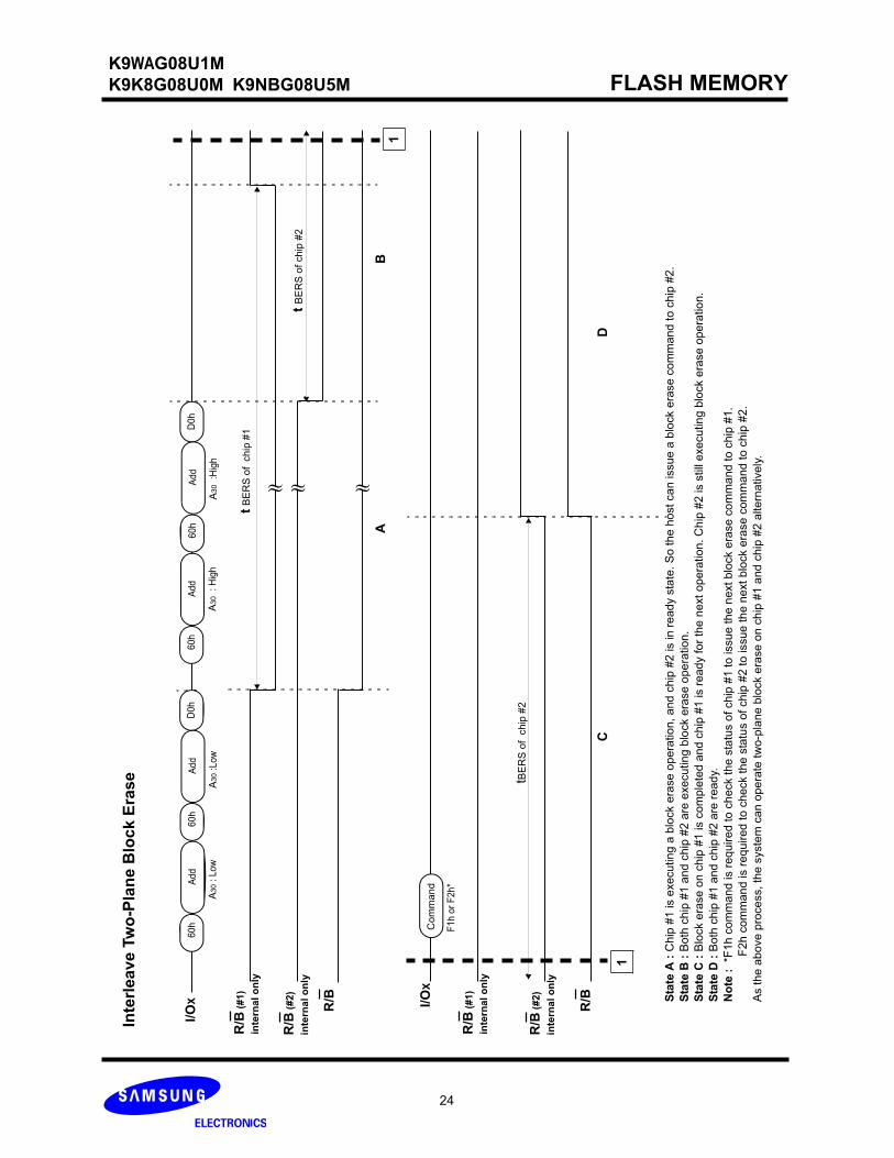
24
K9WAG08U1M
K9K8G08U0M K9NBG08U5M
R/B
(#
1)
I/O
X
Co
mm
an
d
t B
ER
S o
f c
hip
#1
inte
rna
l o
nly
R/B
(#
2)
inte
rna
l o
nly
R/B
60
hD
0h
A30
:Lo
w
Ad
d
60
h
A30 :
Lo
w
Add
F1h
or
F2
h*
60
hD
0h
A30
:H
igh
Ad
d6
0h
A30
: H
igh
Ad
d
t B
ER
S o
f ch
ip #
2
tB
ER
S o
f c
hip
#2
1
1
Inte
rlea
ve
Tw
o-P
lan
e B
loc
k E
rase
R/B
(#
1)
I/O
X
inte
rna
l o
nly
R/B
(#
2)
inte
rna
l o
nly
R/B
AB
C
Sta
te A
: C
hip
#1
is e
xe
cu
tin
g a
blo
ck e
rase
op
era
tio
n,
an
d c
hip
#2
is in
re
ad
y s
tate
. S
o t
he
ho
st
ca
n issu
e a
blo
ck e
rase
co
mm
an
d t
o c
hip
#2
.
Sta
te B
: B
oth
ch
ip #
1 a
nd
ch
ip #
2 a
re e
xe
cu
tin
g b
lock e
rase
op
era
tio
n.
Sta
te C
: B
lock e
rase
on
ch
ip #
1 is c
om
ple
ted
an
d c
hip
#1
is r
ea
dy f
or
the
ne
xt
op
era
tio
n.
Ch
ip #
2 is s
till
exe
cu
tin
g b
lock e
rase
op
era
tio
n.
Sta
te D
: B
oth
ch
ip #
1 a
nd
ch
ip #
2 a
re r
ea
dy.
No
te :
*F
1h
co
mm
an
d is r
eq
uire
d t
o c
he
ck t
he
sta
tus o
f ch
ip #
1 t
o issu
e t
he
ne
xt
blo
ck e
rase
co
mm
an
d t
o c
hip
#1
.
F
2h
co
mm
an
d is r
eq
uire
d t
o c
he
ck t
he
sta
tus o
f ch
ip #
2 t
o issu
e t
he
ne
xt
blo
ck e
rase
co
mm
an
d t
o c
hip
#2
.
As t
he
ab
ove
pro
ce
ss,
the
syste
m c
an
op
era
te t
wo
-pla
ne
blo
ck e
rase
on
ch
ip #
1 a
nd
ch
ip #
2 a
lte
rna
tive
ly.
D
FLASH MEMORY
25
K9WAG08U1M
K9K8G08U0M K9NBG08U5M
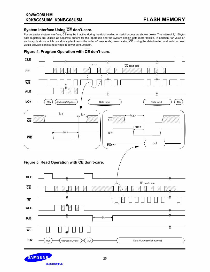
System Interface Using CE don’t-care. For an easier system interface, CE may be inactive during the data-loading or serial access as shown below. The internal 2,112byte
data registers are utilized as separate buffers for this operation and the system design gets more flexible. In addition, for voice or
audio applications which use slow cycle time on the order of -seconds, de-activating CE during the data-loading and serial access
would provide significant savings in power consumption.
Figure 4. Program Operation with CE don’t-care.
CE
WE
tWP
tCHtCS
Address(5Cycles)80h Data Input
CE
CLE
ALE
WE
Data Input
CE don’t-care
10h
Address(5Cycle)00h
CE
CLE
ALE
WE
Data Output(serial access)
CE don’t-care
R/B tR
RE
tCEA
out
tREA
CE
RE
I/O0~7
Figure 5. Read Operation with CE don’t-care.
30h
I/Ox
I/Ox
FLASH MEMORY
26
K9WAG08U1M
K9K8G08U0M K9NBG08U5M
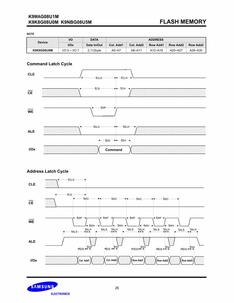
Command Latch Cycle
CE
WE
CLE
ALE
Command
Address Latch Cycle
tCLS
tCS
tCLH
tCH
tWP
tALS tALH
tDS tDH
NOTE
DeviceI/O DATA ADDRESS
I/Ox Data In/Out Col. Add1 Col. Add2 Row Add1 Row Add2 Row Add3
K9K8G08U0M I/O 0 ~ I/O 7 2,112byte A0~A7 A8~A11 A12~A19 A20~A27 A28~A30
I/Ox
CE
WE
CLE
ALE
Col. Add1
tCS
tWC
tWP
tALS
tDStDH
tALH tALS
tWH
tWC
tWP
tDStDH
tALH tALS
tWH
tWC
tWP
tDStDH
tALH tALS
tWH
tDStDH
tWP
I/Ox Col. Add2 Row Add1 Row Add2
tWC
tWH
tALH tALS
tDStDH
Row Add3
tALH
tCLS
FLASH MEMORY
27
K9WAG08U1M
K9K8G08U0M K9NBG08U5M
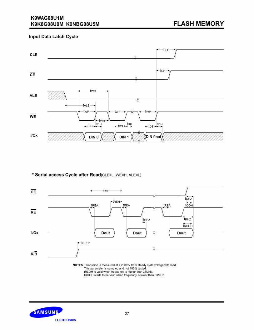
Input Data Latch Cycle
CE
CLE
WE
DIN 0 DIN 1 DIN final
ALE
tALS
tCLH
tWC
tCH
tDStDH
tDStDH
tDStDH
tWP
tWH
tWP tWP
I/Ox
* Serial access Cycle after Read(CLE=L, WE=H, ALE=L)
RE
CE
R/B
Dout Dout Dout
tRC
tREA
tRR
tRHOH
tREA
tREH
tREA tCOH
tRHZ
I/Ox
tCHZ
tRHZ
NOTES : Transition is measured at 200mV from steady state voltage with load. This parameter is sampled and not 100% tested. tRLOH is valid when frequency is higher than 33MHz. tRHOH starts to be valid when frequency is lower than 33MHz.

FLASH MEMORY
28
K9WAG08U1M
K9K8G08U0M K9NBG08U5M
Status Read Cycle & EDC Status Read Cycle
CE
WE
CLE
RE
70h or 7Bh Status Output
tCLR
tCLH
tWP
tCH
tDStDH tREA
tIRtRHOH
tCOHtWHR
tCEA
tCLS
I/Ox
tCHZ
tRHZ
tCS
RE
CE
R/B
I/Ox
tRR
tCEA
tREA
tRP tREH
tRC
tRHZ
tCHZ
Serial Access Cycle after Read(EDO Type, CLE=L, WE=H, ALE=L)
tRHOH
tCOH
tRLOH
Dout Dout
tREA
NOTES : Transition is measured at 200mV from steady state voltage with load. This parameter is sampled and not 100% tested. tRLOH is valid when frequency is higher than 33MHz. tRHOH starts to be valid when frequency is lower than 33MHz.
FLASH MEMORY
29
K9WAG08U1M
K9K8G08U0M K9NBG08U5M
Read Operation(Intercepted by CE)
CE
CLE
R/B
WE
ALE
RE
Busy
00h Dout N Dout N+1 Dout N+2
Row AddressColumn Address
tWB
tAR
tCHZ
tR
tRR
tRC
30h
Read Operation
CE
CLE
R/B
WE
ALE
RE
Busy
00h Col. Add1 Col. Add2 Row Add1 Dout N Dout N+1
Column Address Row Address
tWB
tAR
tR tRCtRHZ
tRR
Dout M
tWC
Row Add2 30h
tCLR
I/Ox
I/Ox Col. Add1 Col. Add2 Row Add1 Row Add2
Row Add3
Row Add3
tCOH

FLASH MEMORY
30
K9WAG08U1M
K9K8G08U0M K9NBG08U5M
Ra
nd
om
Da
ta O
utp
ut
In a
Pa
ge
CE
CL
E
R/B
WE
AL
E
RE
Busy
00h
Dout
ND
out
N+
1
Row
Addre
ssC
olu
mn A
ddre
ss
tWB
tAR
tR tRR
tRC
30h
05h
Colu
mn A
ddre
ss
Dou
t M
Dou
t M+
1I/O
xC
ol.
Add1
Col.
Ad
d2
Row
Add1
Ro
w A
dd2
Col A
dd1
Co
l Ad
d2
Row
Add3
tCL
R E0h
tWH
R
tRE
A

FLASH MEMORY
31
K9WAG08U1M
K9K8G08U0M K9NBG08U5M
Page Program Operation
CE
CLE
R/B
WE
ALE
RE
80h 70h I/O0DinN
Din10h
M
SerialDataInput Command
Column Address Row Address 1 up to m ByteSerial Input
ProgramCommand
Read StatusCommand
I/O0=0 Successful ProgramI/O0=1 Error in Program
tPROGtWB
tWC tWC tWC
I/Ox Co.l Add1 Col. Add2 Row Add1 Row Add2 Row Add3
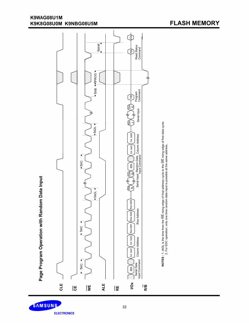
NOTES : tADL is the time from the WE rising edge of final address cycle to the WE rising edge of first data cycle.
tADLtWHR
FLASH MEMORY
32
K9WAG08U1M
K9K8G08U0M K9NBG08U5M
Pag
e P
rog
ram
Op
era
tio
n w
ith
Ra
nd
om
Da
ta I
np
ut
CE
CL
E
R/B
WE
AL
E
RE
80
h70
hI/
O0
Din N
Din
10
hM
Seri
al D
ata
Inp
ut
Co
mm
an
dC
olu
mn
Ad
dre
ss
Ro
w A
dd
ress
Se
ria
l In
pu
tP
rog
ram
Com
man
dR
ea
d S
tatu
sC
om
man
d
tPR
OG
tWB
tWC
tWC
85
h
Ra
ndo
m D
ata
Inp
ut
Com
man
dC
olu
mn
Add
ress
tWC
Din J
Din K
Se
ria
l Inp
ut
I/O
xC
ol.
Add1
Col.
Add2
Row
Add
1R
ow A
dd2
Col.
Add1
Col.
Add2
Row
Add3
NO
TE
S :
1.
tAD
L is t
he
tim
e fro
m t
he W
E r
isin
g e
dg
e o
f fina
l a
dd
ress c
ycle
to
the
WE
ris
ing
ed
ge o
f firs
t d
ata
cycle
.
tAD
L
2
. F
or
ED
C o
pe
ratio
n,
on
ly o
ne t
ime
ra
nd
om
da
ta in
pu
t is
possib
le a
t th
e s
am
e a
dd
ress.
tAD
L
tWH
R

FLASH MEMORY
33
K9WAG08U1M
K9K8G08U0M K9NBG08U5M
Co
py-B
ac
k P
rog
ram
Op
era
tio
n W
ith
Ran
do
m D
ata
In
pu
t
CE
CL
E
R/B
WE
AL
E
RE
00
hI/
Ox
85
h
Colu
mn A
ddre
ssR
ow
Addre
ssR
ead E
DC
Sta
tus
or
Read S
tatu
s C
om
ma
nd
I/O
0=
0 S
ucc
ess
ful P
rogra
mI/
O0=
1 E
rro
r in
Pro
gra
m
tPR
OG
tWB
tWC
Busy
tWB
tR
Busy
10
h
Copy-
Back
Data
Inpu
t C
om
ma
nd
35
h
Colu
mn
Addre
ssR
ow
Addre
ss
Da
ta 1
Data
NI/O
xCo
l Add
1Co
l Add
2Ro
w Ad
d1Ro
w Ad
d2Co
l Add
1Co
l Add
2Ro
w Ad
d1Ro
w Ad
d2Ro
w Ad
d3Ro
w Ad
d37
Bh/7
0h
I/O
1 ~
I/O
2 :
ED
C S
tatu
s (7
Bh
on
ly)
NO
TE
S :
1.
tA
DL
is th
e t
ime
fro
m th
e W
E r
isin
g e
dg
e o
f fin
al a
dd
ress c
ycle
to t
he
WE
ris
ing e
dg
e o
f firs
t d
ata
cycle
.
tAD
L
2. F
or
ED
C o
pe
ratio
n,
on
ly o
ne t
ime
ra
nd
om
da
ta in
pu
t is
possib
le a
t th
e
sa
me a
dd
ress.
tWH
R
FLASH MEMORY
34
K9WAG08U1M
K9K8G08U0M K9NBG08U5M
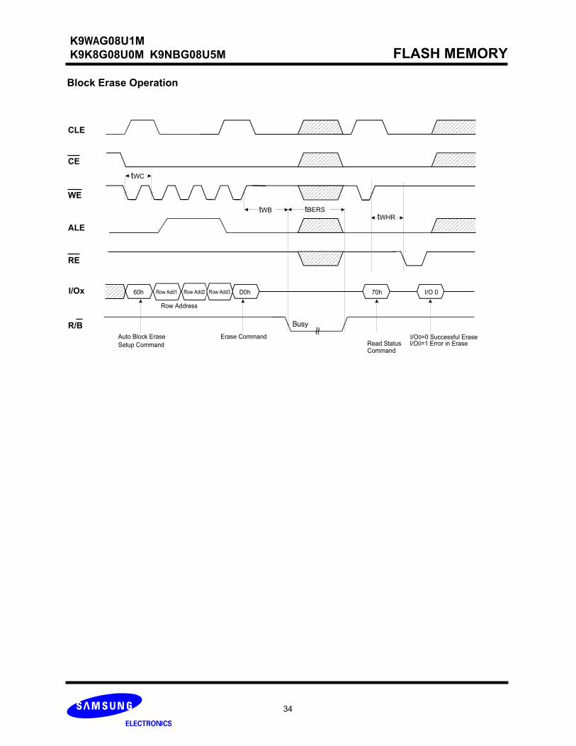
Block Erase Operation
CE
CLE
R/B
WE
ALE
RE
60h
Erase CommandRead StatusCommand
I/O0=1 Error in Erase
D0h 70h I/O 0
Busy
tWB tBERS
I/O0=0 Successful Erase
Row Address
tWC
Auto Block Erase
Setup Command
I/Ox Row Add1 Row Add2 Row Add3
tWHR
FLASH MEMORY
35
K9WAG08U1M
K9K8G08U0M K9NBG08U5M
tWH
R
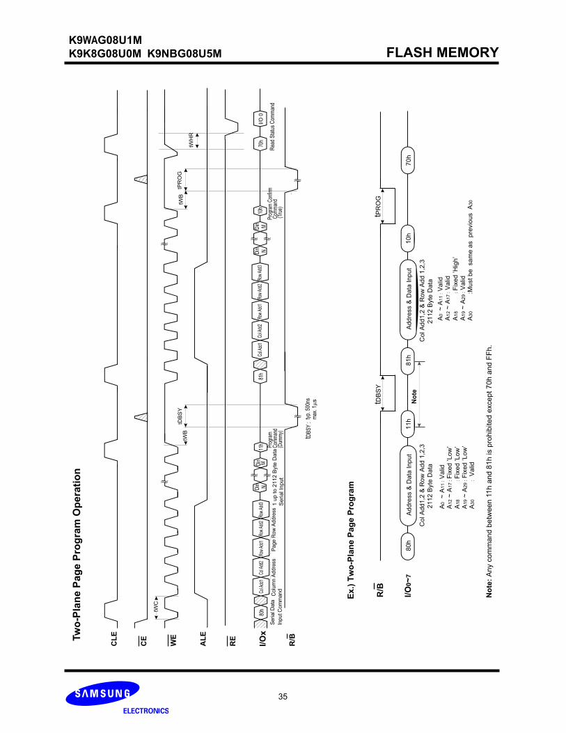
Tw
o-P
lan
e P
ag
e P
rog
ram
Op
era
tio
n
80h
I/O
0~
7
R/B
11
h
Ex
.) T
wo
-Pla
ne P
ag
e P
rog
ram
tDB
SY
Ad
dre
ss &
Da
ta I
np
ut
81h
10
h A
dd
ress &
Data
In
pu
t7
0h
tPR
OG
Co
l A
dd
1,2
& R
ow
Ad
d 1
,2,3
21
12 B
yte
Da
ta
CE
CL
E
R/B
WE
AL
E
RE
80h
Din N
Din
11h
M
Serial D
ata
In
put C
om
mand
Colu
mn A
ddre
ssPr
ogra
m
tDB
SY
tWB
tWC
Com
man
d(D
umm
y)
Din N
10h
tPR
OG
tWB
I/O
0
P
rogr
am C
onfir
mC
omm
and
(Tru
e)
81h
70h
Page R
ow
Addre
ss
I/O
x
1 u
p to
21
12 B
yte
Data
Se
ria
l In
put
Din M
Rea
d S
tatu
s C
omm
and
tDB
SY
:
typ.
500
ns
max
. 1s
Col A
dd1
Col A
dd2
Row
Add1
Row
Add2
Row
Add3
Col A
dd1
Col A
dd2
Row
Add1
Row
Add2
Row
Add3
Col A
dd
1,2
& R
ow
Ad
d 1
,2,3
21
12
Byte
Data
A0 ~
A1
1 : V
alid
A1
2 ~
A17
: F
ixe
d ’L
ow
’
A1
8
: F
ixe
d ’Lo
w’
A1
9 ~
A29
: F
ixed
’L
ow
’
A0
~ A
11
: V
alid
A1
2 ~
A17
: V
alid
A1
8
: F
ixe
d ’H
igh
’ A
19 ~
A29
: V
alid
A3
0
:
V
alid
A3
0
:
Mu
st
be
sa
me
as
pre
vio
us
A30
No
te:
An
y c
om
ma
nd
be
twe
en
11
h a
nd
81
h is p
roh
ibite
d e
xce
pt
70
h a
nd
FF
h.
No
te
FLASH MEMORY
36
K9WAG08U1M
K9K8G08U0M K9NBG08U5M
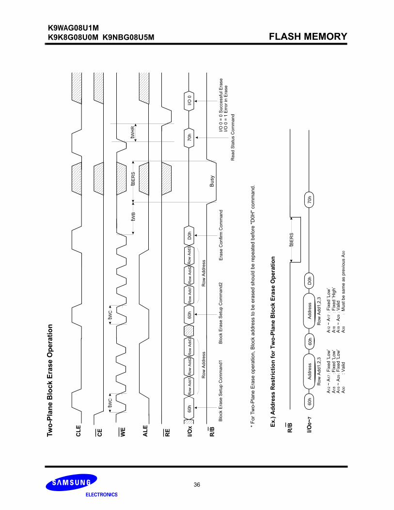
Tw
o-P
lan
e B
loc
k E
rase
Op
era
tio
n
Blo
ck E
rase S
etu
p C
om
ma
nd
1E
rase
Con
firm
Com
man
d
Rea
d S
tatu
sC
om
ma
nd
60h
Ro
w A
dd
1,2
,3
I/O
0~
7
R/B
60h
A9 ~
A25
D0h
tBE
RS
* F
or
Tw
o-P
lan
e E
rase
op
era
tio
n,
Blo
ck a
dd
ress t
o b
e e
rase
d s
ho
uld
be
re
pe
ate
d b
efo
re "
D0
H"
co
mm
an
d.
Ex.)
Ad
dre
ss R
estr
icti
on
fo
r T
wo
-Pla
ne B
lock
Era
se O
pera
tio
n
CE
CL
E
R/B
I/O
X
WE
AL
E
RE
60
hR
ow
Ad
d1
D0
h70
hI/
O 0
Bu
sy
tWB
tBE
RS
tWC
D0h
70
hA
ddre
ss
Add
ress
Row
Add
1,2
,3
I/O
0 =
0 S
uccessfu
l E
rase
I/O
0 =
1 E
rro
r in
Era
se
Ro
w A
dd
2R
ow
Ad
d3
A1
2 ~
A1
7 : F
ixed
’L
ow
’A
18
: F
ixe
d ’L
ow
’A
19 ~
A2
9 : F
ixed
’L
ow
’
A12 ~
A17
: F
ixe
d ’L
ow
’A
18
: F
ixe
d ’H
igh’
A19 ~
A29
: V
alid
A3
0
:
Va
lid
A30
:
Mu
st
be
sa
me a
s p
revio
us A
30
60h
Row
Add
1D
0h
Row
Ad
d2
Ro
w A
dd
3
Ro
w A
ddre
ss
tWC
Blo
ck E
rase
Se
tup
Co
mm
an
d2Ro
w A
ddre
ss
tWH
R
FLASH MEMORY
37
K9WAG08U1M
K9K8G08U0M K9NBG08U5M
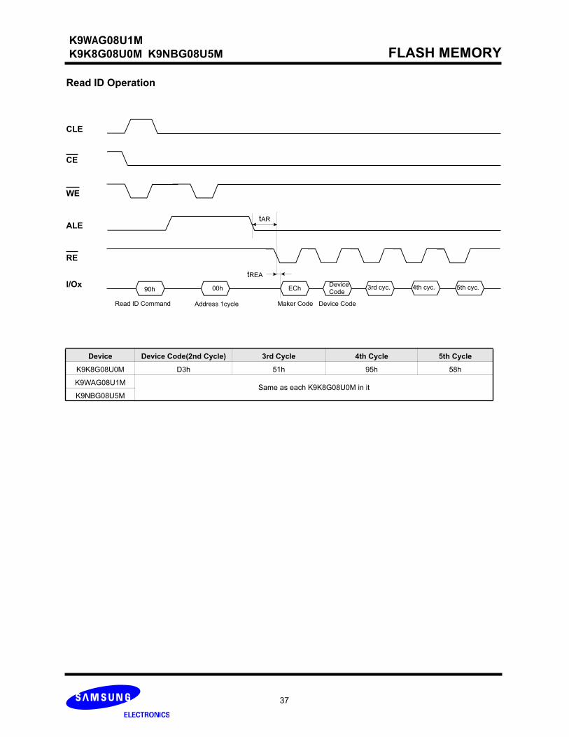
Read ID Operation
CE
CLE
WE
ALE
RE
90h
Read ID Command Maker Code Device Code
00h ECh
tREA
Address 1cycle
I/Ox
tAR
Device Device Code(2nd Cycle) 3rd Cycle 4th Cycle 5th Cycle
K9K8G08U0M D3h 51h 95h 58h
K9WAG08U1MSame as each K9K8G08U0M in it
K9NBG08U5M
Device 4th cyc.Code
3rd cyc. 5th cyc.
FLASH MEMORY
38
K9WAG08U1M
K9K8G08U0M K9NBG08U5M
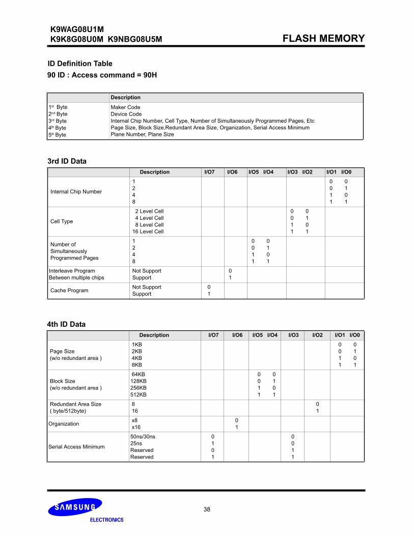
4th ID Data
Description I/O7 I/O6 I/O5 I/O4 I/O3 I/O2 I/O1 I/O0
Page Size
(w/o redundant area )
1KB
2KB
4KB
8KB
0 0
0 1
1 0
1 1
Block Size
(w/o redundant area )
64KB
128KB
256KB
512KB
0 0
0 1
1 0
1 1
Redundant Area Size
( byte/512byte)
8
16
0
1
Organization x8
x16
0
1
Serial Access Minimum
50ns/30ns
25ns
Reserved
Reserved
0
1
0
1
0
0
1
1
ID Definition Table
90 ID : Access command = 90H
Description
1st Byte
2nd Byte
3rd Byte
4th Byte
5th Byte
Maker Code
Device Code
Internal Chip Number, Cell Type, Number of Simultaneously Programmed Pages, Etc
Page Size, Block Size,Redundant Area Size, Organization, Serial Access Minimum
Plane Number, Plane Size
3rd ID Data
Description I/O7 I/O6 I/O5 I/O4 I/O3 I/O2 I/O1 I/O0
Internal Chip Number
1
2
4
8
0 0
0 1
1 0
1 1
Cell Type
2 Level Cell
4 Level Cell
8 Level Cell
16 Level Cell
0 0
0 1
1 0
1 1
Number of
Simultaneously
Programmed Pages
1
2
4
8
0 0
0 1
1 0
1 1
Interleave Program
Between multiple chips
Not Support
Support
0
1
Cache Program Not Support
Support
0
1

FLASH MEMORY
39
K9WAG08U1M
K9K8G08U0M K9NBG08U5M
5th ID Data
Description I/O7 I/O6 I/O5 I/O4 I/O3 I/O2 I/O1 I/O0
Plane Number
1
2
4
8
0 0
0 1
1 0
1 1
Plane Size
(w/o redundant Area)
64Mb
128Mb
256Mb
512Mb
1Gb
2Gb
4Gb
8Gb
0 0 0
0 0 1
0 1 0
0 1 1
1 0 0
1 0 1
1 1 0
1 1 1
Reserved 0 0 0
FLASH MEMORY
40
K9WAG08U1M
K9K8G08U0M K9NBG08U5M
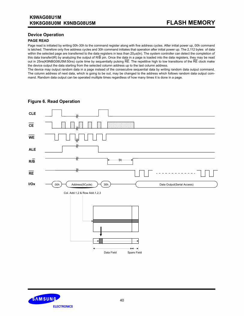
Device Operation
PAGE READ
Page read is initiated by writing 00h-30h to the command register along with five address cycles. After initial power up, 00h command
is latched. Therefore only five address cycles and 30h command initiates that operation after initial power up. The 2,112 bytes of data
within the selected page are transferred to the data registers in less than 20 s(tR). The system controller can detect the completion of
this data transfer(tR) by analyzing the output of R/B pin. Once the data in a page is loaded into the data registers, they may be read
out in 25ns(K9NBG08U5M:50ns) cycle time by sequentially pulsing RE. The repetitive high to low transitions of the RE clock make
the device output the data starting from the selected column address up to the last column address.
The device may output random data in a page instead of the consecutive sequential data by writing random data output command.
The column address of next data, which is going to be out, may be changed to the address which follows random data output com-
mand. Random data output can be operated multiple times regardless of how many times it is done in a page.
Figure 6. Read Operation
Address(5Cycle)00h
Col. Add.1,2 & Row Add.1,2,3
Data Output(Serial Access)
Data Field Spare Field
CE
CLE
ALE
R/B
WE
RE
tR
30hI/Ox

FLASH MEMORY
41
K9WAG08U1M
K9K8G08U0M K9NBG08U5M
Figure 7. Random Data Output In a Page
Address00h Data Output
R/B
RE
tR
30hAddress
05h E0h5Cycles 2CyclesData Output
Data Field Spare Field Data Field Spare Field
I/Ox
Col. Add.1,2 & Row Add.1,2,3
PAGE PROGRAM
The device is programmed basically on a page basis, but it does allow multiple partial page programming of a word or consecutive
bytes up to 2,112, in a single page program cycle. The number of consecutive partial page programming operation within the same
page without an intervening erase operation must not exceed 4 times for a single page. The addressing should be done in sequential
order in a block. A page program cycle consists of a serial data loading period in which up to 2,112bytes of data may be loaded into
the data register, followed by a non-volatile programming period where the loaded data is programmed into the appropriate cell.
The serial data loading period begins by inputting the Serial Data Input command(80h), followed by the five cycle address inputs and
then serial data loading. The words other than those to be programmed do not need to be loaded. The device supports random data
input in a page. The column address for the next data, which will be entered, may be changed to the address which follows random
data input command(85h). Random data input may be operated multiple times regardless of how many times it is done in a page.
Modifying the data of a sector by Random Data Input before Copy-Back Program must be performed for the whole sector
and is allowed only once per each sector. Any partial modification smaller than a sector corrupts the on-chip EDC codes.
The Page Program confirm command(10h) initiates the programming process. Writing 10h alone without previously entering the
serial data will not initiate the programming process. The internal write state controller automatically executes the algorithms and tim-
ings necessary for program and verify, thereby freeing the system controller for other tasks. Once the program process starts, the
Read Status Register command may be entered to read the status register. The system controller can detect the completion of a pro-
gram cycle by monitoring the R/B output, or the Status bit(I/O 6) of the Status Register. Only the Read Status command and Reset
command are valid while programming is in progress. When the Page Program is complete, the Write Status Bit(I/O 0) may be
checked(Figure 8). The internal write verify detects only errors for "1"s that are not successfully programmed to "0"s. The command
register remains in Read Status command mode until another valid command is written to the command register.
Figure 8. Program & Read Status Operation
80h
R/B
Address & Data Input I/O0 Pass
Data
10h 70h
Fail
tPROG
I/Ox
Col. Add.1,2 & Row Add.1,2,3
"0"
"1"
Col. Add.1,2

FLASH MEMORY
42
K9WAG08U1M
K9K8G08U0M K9NBG08U5M
Figure 9. Random Data Input In a Page
80h
R/B
Address & Data Input I/O0 Pass10h 70h
Fail
tPROG
85h Address & Data InputI/Ox
Col. Add.1,2 & Row Add1,2,3 Col. Add.1,2
Data Data
"0"
"1"
Copy-Back Program
The Copy-Back program is configured to quickly and efficiently rewrite data stored in one page without utilizing an external memory.
Since the time-consuming cycles of serial access and re-loading cycles are removed, the system performance is improved. The ben-
efit is especially obvious when a portion of a block is updated and the rest of the block also need to be copied to the newly assigned
free block. The operation for performing a copy-back program is a sequential execution of page-read without serial access and copy-
ing-program with the address of destination page. A read operation with "35h" command and the address of the source page moves
the whole 2,112-byte data into the internal data buffer. As soon as the device returns to Ready state, Page-Copy Data-input com-
mand (85h) with the address cycles of destination page followed may be written. The Program Confirm command (10h) is required to
actually begin the programming operation. During tPROG, the device executes EDC of itself. Once the program process starts, the
Read Status Register command (70h) or Read EDC Status command (7Bh) may be entered to read the status register. The system
controller can detect the completion of a program cycle by monitoring the R/B output, or the Status bit(I/O 6) of the Status Register.
When the Copy-Back Program is complete, the Write Status Bit(I/O 0) and EDC Status Bits (I/O 1 ~ I/O 2) may be checked(Figure 10
& Figure 11& Figure 12). The internal write verification detects only errors for "1"s that are not successfully programmed to "0"s and
the internal EDC checks whether there is only 1-bit error for each 528-byte sector of the source page. More than 2-bit error detection
is not available for each 528-byte sector. The command register remains in Read Status command mode or Read EDC Status com-
mand mode until another valid command is written to the command register.
During copy-back program, data modification is possible using random data input command (85h) as shown in Figure11. But EDC
status Bits are not available during copy back for some bits or bytes modified by Random Data Input operation.
However, in case of the 528 byte sector unit modification, EDC status bits are available.
Figure 10. Page Copy-Back Program Operation
00h
R/B
Add.(5Cycles) I/O0 Pass85h 70h/7Bh
Fail
tPROG
Add.(5Cycles)
tR
Source Address Destination Address
35h 10hI/Ox
Col. Add.1,2 & Row Add.1,2,3Col. Add.1,2 & Row Add.1,2,3
Figure 11. Page Copy-Back Program Operation with Random Data Input
00h
R/B
Add.(5Cycles) 85h 70h
tPROG
Add.(5Cycles)
tR
Source Address Destination Address
Data35h 10h85h DataAdd.(2Cycles)
There is no limitation for the number of repetition.
I/Ox
Col. Add.1,2 & Row Add.1,2,3 Col. Add.1,2 & Row Add.1,2,3 Col. Add.1,2
Note: 1. For EDC operation, only one time random data input is possible at the same address.
Note: 1. Copy-Back Program operation is allowed only within the same memory plane. 2. On the same plane, It’s prohibited to operate copy-back program from an odd address page(source page) to an even
address page(target page) or from an even address page(source page) to an odd address page(target page).
Therefore, the copy-back program is permitted just between odd address pages or even address pages.
"0"
"1"

FLASH MEMORY
43
K9WAG08U1M
K9K8G08U0M K9NBG08U5M
Figure 12. Page Copy-Back Program Operation with EDC & Read EDC Status
00h
R/B
Add.(5Cycles) 85h 7Bh
tPROG
Add.(5Cycles)
tR
Source Address Destination Address
35h 10hI/Ox
Col. Add.1,2 & Row Add.1,2,3Col. Add.1,2 & Row Add.1,2,3
EDC Status Output
Figure 13. Block Erase Operation
BLOCK ERASE
The Erase operation is done on a block basis. Block address loading is accomplished in three cycles initiated by an Erase Setup
command(60h). Only address A18 to A30 is valid while A12 to A17 is ignored. The Erase Confirm command(D0h) following the block
address loading initiates the internal erasing process. This two-step sequence of setup followed by execution command ensures that
memory contents are not accidentally erased due to external noise conditions.
At the rising edge of WE after the erase confirm command input, the internal write controller handles erase and erase-verify. When
the erase operation is completed, the Write Status Bit(I/O 0) may be checked. Figure 13 details the sequence.
60h
Row Add 1,2,3
R/B
Address Input(3Cycle) I/O0 PassD0h 70h
Fail
tBERS
I/Ox
"0"
"1"
EDC OPERATIONNote that for the user who use Copy-Back with EDC mode, only one time random data input is possible at the same address during
Copy-Back program or page program mode. For the user who use Copy-Back without EDC, there is no limitation for the random data
input at the same address.
Two-Plane Page Program
Two-Plane Page Program is an extension of Page Program, for a single plane with 2112 byte page registers. Since the device is
equipped with four memory planes, activating the two sets of 2112 byte page registers enables a simultaneous programming of two
pages. But there is some restriction, two-plane program operations can be executed by dividing the memory array into plane 0~1 or
plane 2~3 separately. For example, two-plane program operation into plane 0 and plane 2 is prohibited. That is to say, two-plane pro-
gram operation into plane 0 and plane 1 or into plane 2 and plane 3 is allowed.
After writing the first set of data up to 2112 byte into the selected page register, Dummy Page Program command (11h) instead of
actual Page Program command (10h) is inputted to finish data-loading of the first plane. Since no programming process is involved,
R/B remains in Busy state for a short period of time(tDBSY). Read Status command (70h) may be issued to find out when the device
returns to Ready state by polling the Ready/Busy status bit(I/O 6). Then the next set of data for the other plane is inputted after the
81h command and address sequences. After inputting data for the last plane, actual True Page Program(10h) instead of dummy
Page Program command (11h) must be followed to start the programming process. The operation of R/B and Read Status is the
same as that of Page Program. Althougth two planes are programmed simultaneously, pass/fail is not available for each page when
the program operation completes. Status bit of I/O 0 is set to "1" when any of the pages fails.
Restriction in addressing with Two-Plane Page Program is shown is Figure14.
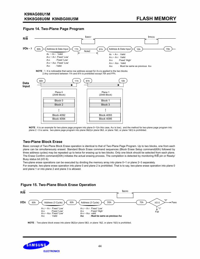
FLASH MEMORY
44
K9WAG08U1M
K9K8G08U0M K9NBG08U5M
Figure 14. Two-Plane Page Program
80h 11hDataInput
Plane 0(2048 Block)
Block 0
Block 2
Block 4094
Block 4092
80hI/O0 ~ 7
R/B
Address & Data Input 11h 81h 10h
tDBSY tPROG
70h Address & Data Input
NOTE : 1. It is noticeable that same row address except for A18 is applied to the two blocks
81h 10h
Plane 1(2048 Block)
Block 1
Block 3
Block 4095
Block 4093
Figure 15. Two-Plane Block Erase Operation
60hI/OX
R/B
60h D0h I/O 0 Pass
Fail
tBERS
Address (3 Cycle) Address (3 Cycle) 70h"0"
"1"A12 ~ A17 : Fixed ’Low’A18 :Fixed ’Low’A19 ~ A29 : Fixed ’Low’
A12 ~ A17 : Fixed ’Low’A18 : Fixed ’High’A19 ~ A29 : valid
Two-Plane Block Erase Basic concept of Two-Plane Block Erase operation is identical to that of Two-Plane Page Program. Up to two blocks, one from each
plane can be simultaneously erased. Standard Block Erase command sequences (Block Erase Setup command(60h) followed by
three address cycles) may be repeated up to twice for erasing up to two blocks. Only one block should be selected from each plane.
The Erase Confirm command(D0h) initiates the actual erasing process. The completion is detected by monitoring R/B pin or Ready/
Busy status bit (I/O 6).
Two-plane erase operations can be executed by dividing the memory array into plane 0~1 or plane 2~3 separately.
For example, two-plane erase operation into plane 0 and plane 2 is prohibited. That is to say, two-plane erase operation into plane 0
and plane 1 or into plane 2 and plane 3 is allowed.
A0 ~ A11 : Valid
A12 ~ A17 : Fixed ’Low’
A18 : Fixed ’Low’
A19 ~ A29 : Fixed ’Low’
A30 : Valid
A0 ~ A11 : Valid
A12 ~ A17 : Valid
A18 : Fixed ’High’
A19 ~ A29 : Valid
A30 : Must be same as previous A30
A30 : Valid A30 : must be same as previous A30
NOTE : It is an example for two-plane page program into plane 0~1(In this case, A30 is low), and the method for two-plane page program into plane 2 ~3 is same. two-plane page program into plane 0&2(or plane 0&3, or plane 1&2, or plane 1&3) is prohibited.
NOTE : Two-plane block erase into plane 0&2(or plane 0&3, or plane 1&2, or plane 1&3) is prohibited.
2.Any command between 11h and 81h is prohibited except 70h and FFh.
Note2
A30 : Must be same as previous A30
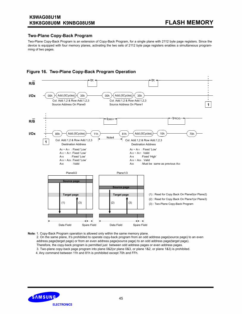
FLASH MEMORY
45
K9WAG08U1M
K9K8G08U0M K9NBG08U5M
Figure 16. Two-Plane Copy-Back Program Operation
R/B
85h 70h
tPROG
Add.(5Cycles)
Destination Address
10hI/Ox
Col. Add.1,2 & Row Add.1,2,3
81h Add.(5Cycles)
Destination Address
Col. Add.1,2 & Row Add.1,2,3
00h
R/B
Add.(5Cycles)
tR
Source Address On Plane0
35hI/Ox
Col. Add.1,2 & Row Add.1,2,3
00h Add.(5Cycles)
Source Address On Plane1
35h
Col. Add.1,2 & Row Add.1,2,3
tR
11h
tDBSY
Two-Plane Copy-Back Program
Two-Plane Copy-Back Program is an extension of Copy-Back Program, for a single plane with 2112 byte page registers. Since the
device is equipped with four memory planes, activating the two sets of 2112 byte page registers enables a simultaneous program-
ming of two pages.
Data Field Spare Field Data Field Spare Field
(1) (2)(3) (3)
Plane0/2 Plane1/3
Source page
Target page
Source page
Target page (1) : Read for Copy Back On Plane0(or Plane2)
(2) : Read for Copy Back On Plane1(or Plane3)
(3) : Two-Plane Copy-Back Program
A0 ~ A11 : Fixed ’Low’
A12 ~ A17 : Fixed ’Low’
A18 : Fixed ’Low’
A19 ~ A29 : Fixed ’Low’
A30 : Valid
A0 ~ A11 : Fixed ’Low’
A12 ~ A17 : Valid
A18 : Fixed ’High’
A19 ~ A29 : Valid
A30 : Must be same as previous A30
1
1
Note: 1. Copy-Back Program operation is allowed only within the same memory plane. 2. On the same plane, It’s prohibited to operate copy-back program from an odd address page(source page) to an even
address page(target page) or from an even address page(source page) to an odd address page(target page).
Therefore, the copy-back program is permitted just between odd address pages or even address pages.
3. Two-plane copy-back page program into plane 0&2(or plane 0&3, or plane 1&2, or plane 1&3) is prohibited.
4. Any command between 11h and 81h is prohibited except 70h and FFh.
Note4
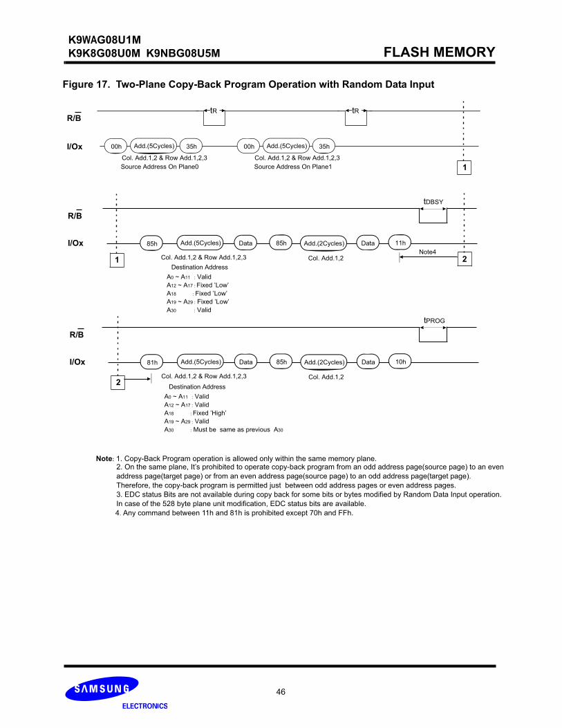
FLASH MEMORY
46
K9WAG08U1M
K9K8G08U0M K9NBG08U5M
R/B
85h 11h
tDBSY
Add.(5Cycles) Data 85h DataI/Ox
Col. Add.1,2 & Row Add.1,2,3 Col. Add.1,2
Add.(2Cycles)
00h
R/B
Add.(5Cycles)
tR
Source Address On Plane0
35hI/Ox
Col. Add.1,2 & Row Add.1,2,3
00h Add.(5Cycles)
Source Address On Plane1
35h
Col. Add.1,2 & Row Add.1,2,3
tR
1
R/B
81h 10h
tPROG
Add.(5Cycles) Data 85h DataI/Ox
Col. Add.1,2 & Row Add.1,2,3 Col. Add.1,2
Add.(2Cycles)
1 2
2
Destination Address
A0 ~ A11 : Valid
A12 ~ A17 : Fixed ’Low’
A18 : Fixed ’Low’
A19 ~ A29 : Fixed ’Low’
A30 : Valid
Destination Address
A0 ~ A11 : Valid
A12 ~ A17 : Valid
A18 : Fixed ’High’
A19 ~ A29 : Valid
A30 : Must be same as previous A30
Figure 17. Two-Plane Copy-Back Program Operation with Random Data Input
Note: 1. Copy-Back Program operation is allowed only within the same memory plane. 2. On the same plane, It’s prohibited to operate copy-back program from an odd address page(source page) to an even
address page(target page) or from an even address page(source page) to an odd address page(target page).
Therefore, the copy-back program is permitted just between odd address pages or even address pages.
3. EDC status Bits are not available during copy back for some bits or bytes modified by Random Data Input operation.
In case of the 528 byte plane unit modification, EDC status bits are available.
4. Any command between 11h and 81h is prohibited except 70h and FFh.
Note4
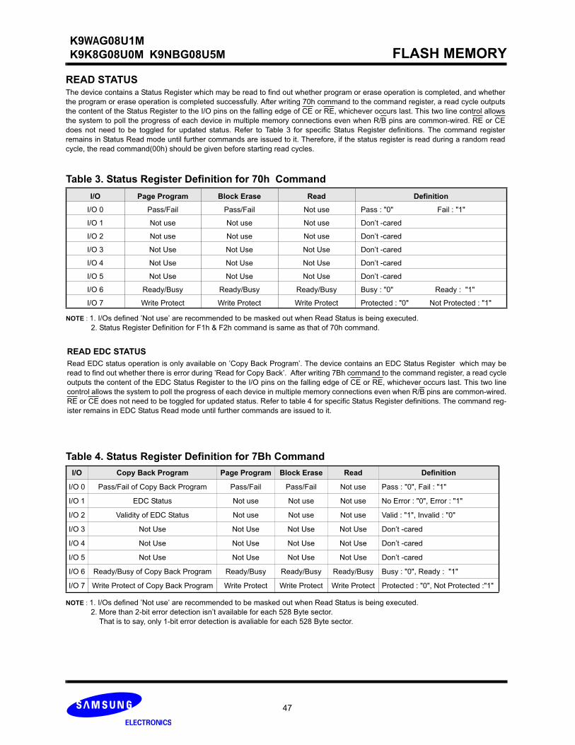
FLASH MEMORY
47
K9WAG08U1M
K9K8G08U0M K9NBG08U5M
READ STATUSThe device contains a Status Register which may be read to find out whether program or erase operation is completed, and whether
the program or erase operation is completed successfully. After writing 70h command to the command register, a read cycle outputs
the content of the Status Register to the I/O pins on the falling edge of CE or RE, whichever occurs last. This two line control allows
the system to poll the progress of each device in multiple memory connections even when R/B pins are common-wired. RE or CE
does not need to be toggled for updated status. Refer to Table 3 for specific Status Register definitions. The command register
remains in Status Read mode until further commands are issued to it. Therefore, if the status register is read during a random read
cycle, the read command(00h) should be given before starting read cycles.
Table 3. Status Register Definition for 70h Command
NOTE : 1. I/Os defined ’Not use’ are recommended to be masked out when Read Status is being executed.
2. Status Register Definition for F1h & F2h command is same as that of 70h command.
I/O Page Program Block Erase Read Definition
I/O 0 Pass/Fail Pass/Fail Not use Pass : "0" Fail : "1"
I/O 1 Not use Not use Not use Don’t -cared
I/O 2 Not use Not use Not use Don’t -cared
I/O 3 Not Use Not Use Not Use Don’t -cared
I/O 4 Not Use Not Use Not Use Don’t -cared
I/O 5 Not Use Not Use Not Use Don’t -cared
I/O 6 Ready/Busy Ready/Busy Ready/Busy Busy : "0" Ready : "1"
I/O 7 Write Protect Write Protect Write Protect Protected : "0" Not Protected : "1"
READ EDC STATUS
Read EDC status operation is only available on ’Copy Back Program’. The device contains an EDC Status Register which may be
read to find out whether there is error during ’Read for Copy Back’. After writing 7Bh command to the command register, a read cycle
outputs the content of the EDC Status Register to the I/O pins on the falling edge of CE or RE, whichever occurs last. This two line
control allows the system to poll the progress of each device in multiple memory connections even when R/B pins are common-wired.
RE or CE does not need to be toggled for updated status. Refer to table 4 for specific Status Register definitions. The command reg-
ister remains in EDC Status Read mode until further commands are issued to it.
Table 4. Status Register Definition for 7Bh Command
NOTE : 1. I/Os defined ’Not use’ are recommended to be masked out when Read Status is being executed.
2. More than 2-bit error detection isn’t available for each 528 Byte sector.
That is to say, only 1-bit error detection is avaliable for each 528 Byte sector.
I/O Copy Back Program Page Program Block Erase Read Definition
I/O 0 Pass/Fail of Copy Back Program Pass/Fail Pass/Fail Not use Pass : "0", Fail : "1"
I/O 1 EDC Status Not use Not use Not use No Error : "0", Error : "1"
I/O 2 Validity of EDC Status Not use Not use Not use Valid : "1", Invalid : "0"
I/O 3 Not Use Not Use Not Use Not Use Don’t -cared
I/O 4 Not Use Not Use Not Use Not Use Don’t -cared
I/O 5 Not Use Not Use Not Use Not Use Don’t -cared
I/O 6 Ready/Busy of Copy Back Program Ready/Busy Ready/Busy Ready/Busy Busy : "0", Ready : "1"
I/O 7 Write Protect of Copy Back Program Write Protect Write Protect Write Protect Protected : "0", Not Protected :"1"
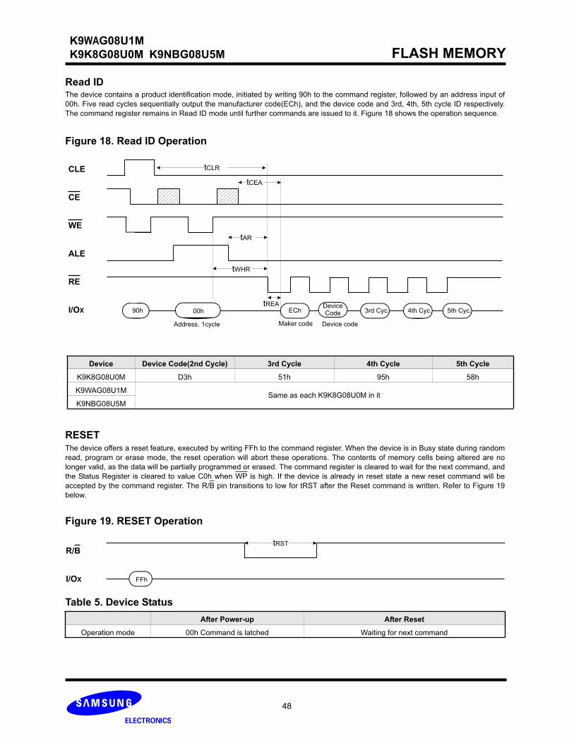
FLASH MEMORY
48
K9WAG08U1M
K9K8G08U0M K9NBG08U5M
Figure 18. Read ID Operation
CE
CLE
I/OX
ALE
RE
WE
90h 00h
Address. 1cycle Maker code Device code
tCEA
tAR
tREA
Read IDThe device contains a product identification mode, initiated by writing 90h to the command register, followed by an address input of
00h. Five read cycles sequentially output the manufacturer code(ECh), and the device code and 3rd, 4th, 5th cycle ID respectively.
The command register remains in Read ID mode until further commands are issued to it. Figure 18 shows the operation sequence.
Figure 19. RESET Operation
RESET
The device offers a reset feature, executed by writing FFh to the command register. When the device is in Busy state during random
read, program or erase mode, the reset operation will abort these operations. The contents of memory cells being altered are no
longer valid, as the data will be partially programmed or erased. The command register is cleared to wait for the next command, and
the Status Register is cleared to value C0h when WP is high. If the device is already in reset state a new reset command will be
accepted by the command register. The R/B pin transitions to low for tRST after the Reset command is written. Refer to Figure 19
below.
FFhI/OX
R/BtRST
tWHR
tCLR
ECh
Device Device Code(2nd Cycle) 3rd Cycle 4th Cycle 5th Cycle
K9K8G08U0M D3h 51h 95h 58h
K9WAG08U1MSame as each K9K8G08U0M in it
K9NBG08U5M
Device4th Cyc.Code 3rd Cyc. 5th Cyc.
Table 5. Device Status
After Power-up After Reset
Operation mode 00h Command is latched Waiting for next command

FLASH MEMORY
49
K9WAG08U1M
K9K8G08U0M K9NBG08U5M
READY/BUSY
The device has a R/B output that provides a hardware method of indicating the completion of a page program, erase and random
read completion. The R/B pin is normally high but transitions to low after program or erase command is written to the command regis-
ter or random read is started after address loading. It returns to high when the internal controller has finished the operation. The pin is
an open-drain driver thereby allowing two or more R/B outputs to be Or-tied. Because pull-up resistor value is related to tr(R/B) and
current drain during busy(ibusy) , an appropriate value can be obtained with the following reference chart(Fig.20). Its value can be
determined by the following guidance.
VCC
R/Bopen drain output
Device
GND
Rp
tr,t
f [s
]
Ibu
sy
[A
]
Rp(ohm)
Figure 20. Rp vs tr ,tf & Rp vs ibusy
Ibusy
tr
ibusy
Busy
Ready Vcc
@ Vcc = 3.3V, Ta = 25 C , CL = 50pF
VOH
tf tr
1K 2K 3K 4K
50n
100n
150n 3m
2m
1m50
tf
100
150
200
1.8 1.8 1.8 1.8
2.4
1.2
0.8
0.6
VOL
where IL is the sum of the input currents of all devices tied to the R/B pin.
Rp value guidance
Rp(max) is determined by maximum permissible limit of tr
Rp(min, 3.3V part) =VCC(Max.) - VOL(Max.)
IOL + IL =
3.2V
8mA + IL
3.3V device - VOL : 0.4V, VOH : 2.4V
CL
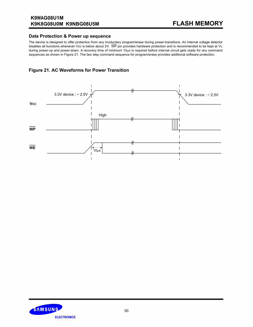
FLASH MEMORY
50
K9WAG08U1M
K9K8G08U0M K9NBG08U5M
Data Protection & Power up sequence
The device is designed to offer protection from any involuntary program/erase during power-transitions. An internal voltage detector
disables all functions whenever Vcc is below about 2V. WP pin provides hardware protection and is recommended to be kept at VIL
during power-up and power-down. A recovery time of minimum 10 s is required before internal circuit gets ready for any command
sequences as shown in Figure 21. The two step command sequence for program/erase provides additional software protection.
Figure 21. AC Waveforms for Power Transition
VCC
WP
High
WE
3.3V device : ~ 2.5V 3.3V device : ~ 2.5V
10 s