Embed Size (px)
Citation preview

Philips tech. Rev. 32, 345-360, 1971, No. 9/10/11/12
IMP ATT -diode oscillators
K. Mouthaan
Introduetion
Microwave energy can be produced with variouskinds of semiconductor devices, and of the variouspractical possibilities the IMPATT-diode oscillator ispotentially the most powerful. The physics and technol-ogy of the IMPATT diode, the active element in thisoscillator, have been dealt with in detail in the preced-ing article [11. In the present article we shall considerthe IMPATT-diode oscillator as a whole, confiningourselves to oscillators that deliver c.w. microwaveenergy.
A simple oscillator construction is shown in jig. 1.It consists of a coaxial line with the diode mounted inthe varactor package A at the end of the line. Thecoaxial output, which has a given characteristic imped-ance Zo, is matched to the diode with a quarter-wavetransformer T. The frequency of the microwave energyproduced is determined by the distance from T to A.An experimental model of an oscillator designed alongthese lines is shown in fig. 11. Fig. 2 shows the operat-ing point of the diode on the current-voltage charac-teristic: the diode is reverse-biased into the breakdownregion. The d.c. current through the diode is kept at a
Fig. 1. A coaxial IMPATI-diode oscillator. A varactor packagecontaining the active element, the IMPATI diode. The diode issupplied by a d.c. current 10. The oscillator output is at the left.T quarter-wave transformer for matching the coaxial line to thediode. Zo characteristic impedance of the coaxialline. The oscil-lation frequency is determined by the distance from T to A. Seealso fig. l l ,
constant value 10 by using a current source. The d.c.voltage Vo across the diode is usually not very differentfrom the breakdown voltage Vb. The microwave out-put power can be controlled by varying 10. Fig. 3shows the output power and efficiency of an IMPATT-diode oscillator for 5 GHz.
Dr. Ir. K. Mouthaan is with Philips Research Laboratories,Eindhoven.
I
1Ia
p
~o
o -vFig. 2. Current-voltage characteristic of a diode (schematic). Thediode is reverse-biased by a voltage high enough to cause break-down. The diode is set to the operating point P(Vo,lo) by meansof a d.c. current source (a source with a high internal resistance).The current and voltage in the reverse direction are shown hereas positive, which is the only direction ofimportance here, unlikethe situation with ordinary semiconductor diodes, in which theforward direction is also important.
1.5~'.------------------------;5%A
10
2
Fig. 3. Microwave output power Po and efficiency 'I) as a functionof the d.c. current 10 of a c.w. oscillator for 5 GHz, of the typeshown in fig. 1.
[1] D. de Nobel and M. T. Vlaardingerbroek, IMPATI diodes;this issue, page 328.
1.0
r 0.5"' ....
""""'"//III
02
60 80---Ia
346 K.MOUTHAAN Philips tech. Rev. 32, No. 9/10/11/12
In this article a few general performance character-istics of the oscillator will be discussed first: the levelof oscillation, the output power, the efficiency and thestarting current. Equivalent circuits for the diode andthe oscillator will be produced which give a convenientsurvey of the microwave behaviour. These equivalentcircuits are important aids in oscillator design. Twoof the oscillators investigated at these Laboratories willthen be discussed [21, and we shall examine some ofthe factors that determine the stability of an oscillator.This will be followed by a brief discussion of noise, andin conclusion we shalliook at the possibility of improv-ing the characteristics of an oscillator by tuning tohigher harmonics.
Equivalent circuit of the IMPATT diode
To arrive at an equivalent circuit for the diode, weshall first summarize the behaviour of the diode ford.c. and a.c. applied voltages.Let us consider a reverse-biased P+-N-N+ diode in the
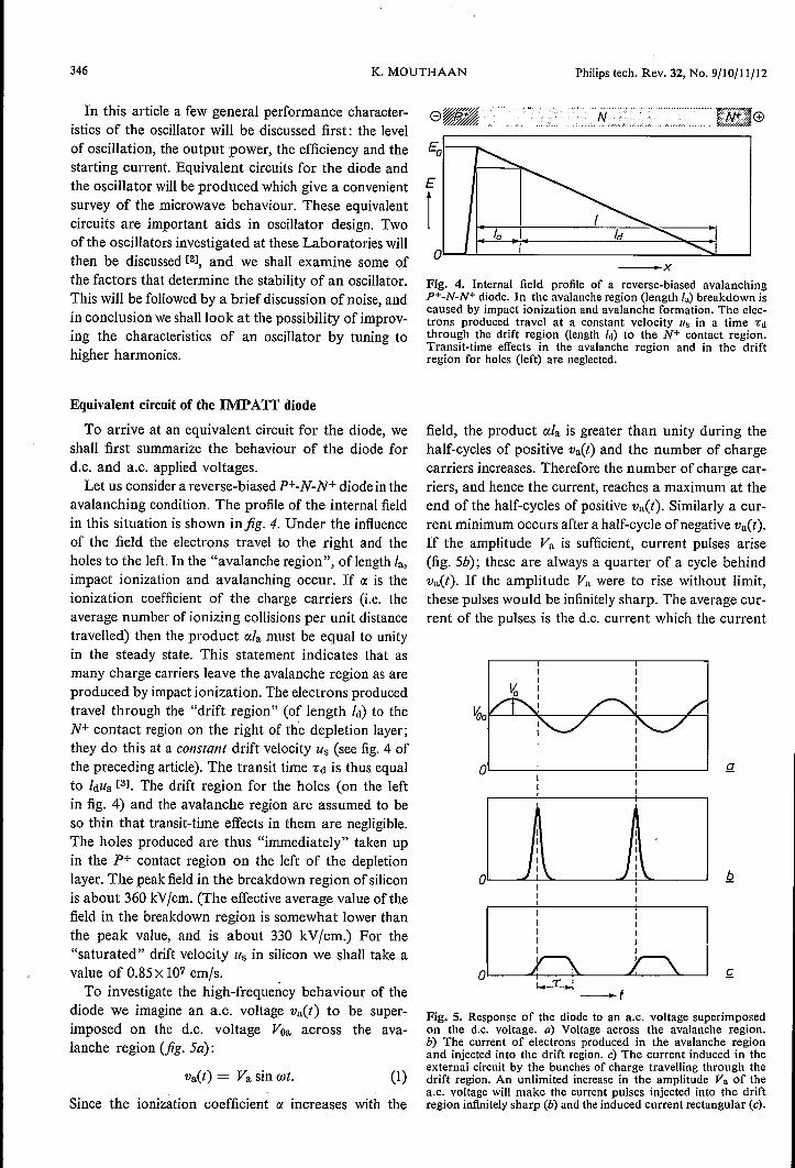
avalanching condition. The profile of the internal fieldin this situation is shown infig. 4. Under the influenceof the field the electrons travel to the right and theholes to the left. In the "avalanche region", oflength la,impact ionization and avalanching occur. If a is theionization coefficient of the charge carriers (i.e. theaverage number of ionizing collisions per unit distancetravelled) then the product ala must be equal to unityin the steady state. This statement indicates that asmany charge carriers leave the avalanche region as areproduced by impact ionization. The electrons producedtravel through the "drift region" (of length Id) to theN+ contact region on the right of the depletion layer;they do this at a constant drift velocity Us (see fig. 4 ofthe preceding article). The transit time id is thus equalto Ieu« [31. The drift region for the holes (on the leftin fig. 4) and the avalanche region are assumed to beso thin that transit-time effects in them are negligible.The holes produced are thus "immediately" taken upin the P+ contact region on the left of the depletionlayer. The peak field in the breakdown region of siliconis about 360 kV/cm. (The effective average value ofthefield in the breakdown region is somewhat lower thanthe peak value, and is about 330 kV/cm.) For the"saturated" drift velocity Us in silicon we shall take avalue of 0.85X 107 cm/so .To investigate the high-frequency behaviour of the
diode we imagine an a.c. voltage va(t) to be super-imposed on the d.c. voltage Voa across the ava-lanche region (fig. 5a):
Va(t) = Va sin cot.
Since the ionization coefficient a increases with the
-xFig. 4. Internal field profile of a reverse-biased avalanchingP+-N-N+ diode. In the avalanche region (length la) breakdown iscaused by impact ionization and avalanche formation. The elec-trons produced travel at a constant velocity lis in a time Td
through the drift region (length Id) to the N+ contact region.Transit-time effects in the avalanche region and in the driftregion for holes (left) are neglected.
field, the product IX/a is greater than unity during thehalf-cycles of positive va(t) and the number of chargecarriers increases. Therefore the number of charge car-riers, and hence the current, reaches a maximum at theend of the half-cycles of positive va(t). Similarly a cur-rent minimum occurs after a half-cycle ofnegative vaCt).If the amplitude Va is sufficient, current pulses arise(fig. 5b); these are always a quarter of a cycle behindva(t). If the amplitude Va were to rise without limit,these pulses would be infinitely sharp. The average cur-rent of the pulses is the d.c. current which the current
o~---+----------~----~
I ~I II II I
J:\ I
):\o I
(1)
I.--!---.j - t
Fig. 5. Response of the diode to an a.c, voltage superimposedon the d.c. voltage. a) Voltage across the avalanche region.b) The current of electrons produced in the avalanche regionand injected into the drift region. c) The current induced in theexternal circuit by the bunches of charge travelling through thedrift region. An unlimited increase in the amplitude Va of thea.c. voltage will make the current pulses injected into the driftregion infinitely sharp (b) and the induced current rectangular (c).

Philips tech. Rev. 32, No. 9/10/11/12 IMPATT-DIODE OSCILLATORS 347
source maintains constant at the value 10. The funda-mental (angular frequency co), like all the harmonics,has an amplitude 2/0 in the limiting case of infinitelysharp current pulses. Since the fundamental is also 90°in phase behind va(t), it takes the form:
ica(t) = -2/0 cos wt.
A bunch of electrons generated in the avalanche V;layer, and corresponding to one current pulse, travelsthrough the drift region at the velocity Us in the time <d.During its transit time this bunch of electrons, travel-ling at constant velocity, induces a constant current inthe circuit connected to the diode. The successivebunches of charge thus give rise to a series of rectangu-lar pulses of current in the external circuit (fig. 5c).Calculation of the fundamental of this induced currentgives:
ii(t) = -2/0«(jjl cos ost+ o« sin wt), (3)where
(jj _ sin e(4a)l--e-,
sin'' !e(4b)(jj2 =-- te
and e = W<d = Wld/US' (4c)
The quantity e is the transit angle. An essential featurein the operation of the IMPATT diode is the phasedifference between het) and ica(t), expressed in equa-tion (3) by the term (jj2 sin wt. This phase differenceis a transit-time effect: (jj2 only differs from 0when e, and hence id, differs from O.
The currents mentioned so far are conduction cur-rents, carried by electrons and holes. In addition,capacitive currents occur both in the avalanche regionand in the drift region.The equivalent circuit that can be drawn on the basis
of these data [4] is shown infig. 6. The conduction cur-rents ica(t) and ii(t) (eqs. 2 and 3) are represented bycurrent sources, the capacitive character of the ava-lanche region and drift region by capacitors Ca and Cd.The resistance R; represents losses in the diode.The two terms that form ii(t) in (3) are each repre-
sented by a current source. There are therefore threecurrent sources in all; two of them (ica(t) and the firstterm of ir(t)) are 90° behind va(t) in phase. This isexpressed by the factor +j in the complex notationwe shall use here. The third source (the second termof ii(t)), which represents the transit-time effect, is inantiphase with va(t).At finite values ofthe amplitude Va the current pulses
are not infinitely sharp. Although the phase relationsremain the same, the conduction current in the ava-
(2)
+
+
Fig. 6. Equivalent circuit of the IMPATT diode for signals ofangular frequency w. Ca and Cd are the capacitances of the ava-lanche and drift regions. Rs is the loss resistance of the diode.The complex amplitudes are given for the voltages and currents.Va, Vd, Vt are the amplitudes of the voltages across the avalancheregion, the drift region and the complete diode. The current source2jf3Io represents the first Fourier component ica(t) (see eq. 2) ofthe series of current pulses in fig. 5b. The two other sources repre-sent the two terms of het) (see eq. 3), which are the in-phase and90° out-of-phase components of the current of rectangular pulsesin fig. 5c. These terms are dependent through (jh and (/h on thetransit angle 8, i.e. on the frequency (see eq. 4c). The factor f3is equal to 1 in the limiting case of infinitely large Va; f3 forfinite Va is given in fig. 7.
(The complex exponential notation used here also expressesthe phase relationships. The voltage polarities and current direc-tions indicated are the positive directions for the calculation.The bars above Vd and Vt indicate that these amplitudes arecomplex, i.e. the a.c. voltages Vd(t) and Vt(t) over the drift regionand the complete diode are not in phase with va(t). The factor f3is real. A factor j implies a 90° phase lead with respect to a realcurrent in the direction indicated by the arrows.)
lanche region is smaller than that given by equa-tion (2). This is allowed for in the equivalent circuit bythe factor {3, which is real and cannot exceed the value I.Since the relation between the current in the drift regionand the current in the avalanche region is linear, wecan use the same factor {3 in the three current sources.Fig. 7 shows {3, obtained from a more detailed analysis,as a function of Va [5]. The value VI plotted horizon-tally in fig. 7 is a normalized value of Va. The relationbetween VI and Va is:
(5)
In this expression Cl.c' is the derivative of the ionizationcoefficient Cl. with respect to the field-strength at theoperating point, and <a is the transit time in the ava-
[2] The diodes for these oscillators were made at these labora-tories by Dr. D. de Nobel and H. G. Koek.
[3] In the preceding article this transit time in the drift regionwas indicated by 1:.
[4] K. Mouthaan, Characterization of nonlinear interactions inavalanche transit-time oscillators, frequency multipliers, andfrequency dividers, IEEE Trans. MTT-18, 853-862, 1970.
[5] Fig. 7 is equivalent 'to fig. 8 in the preceding article. Thevariable Vl is equal to tgVa in the Appendix of that article.
'348 K. MOUTHAAN Philips tech. Rev. 32, No. 9/10/11/12
lanche region. If VOa is the d.c. voltage across the ava-lanche region, then in silicon !Xc' can in practice beequated with 5/Voa.
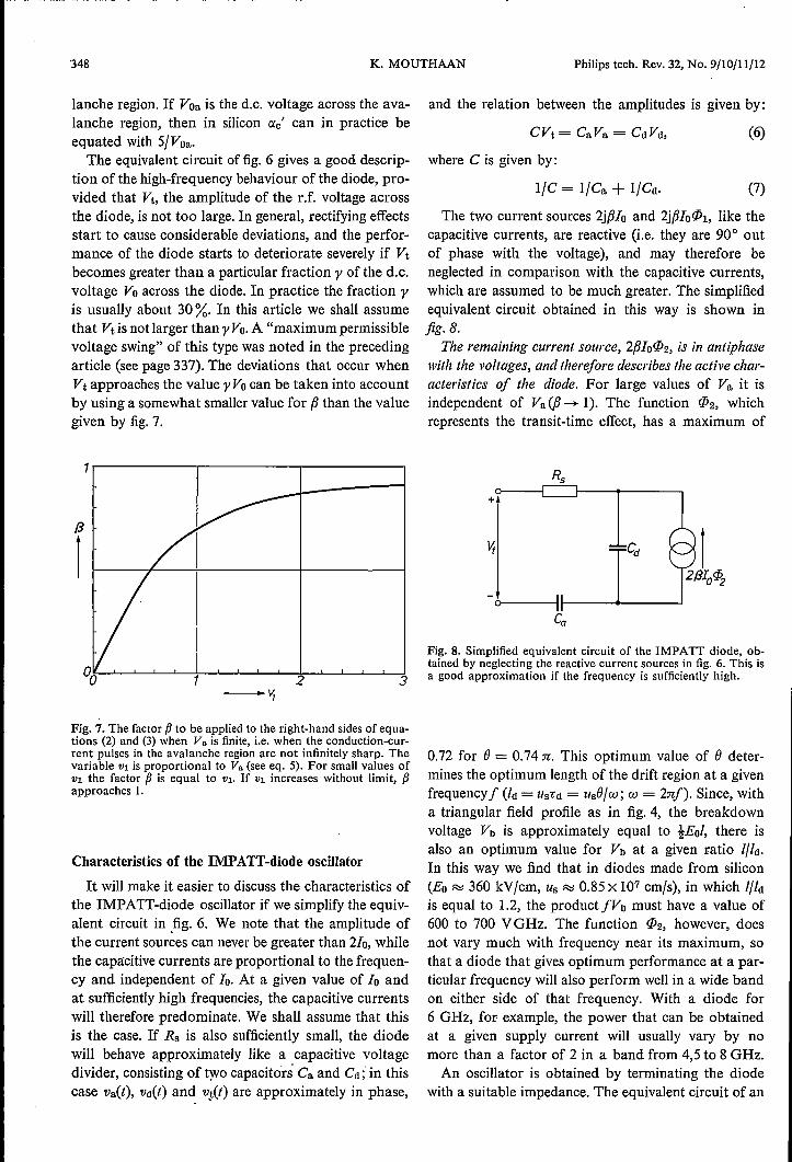
The equivalent circuit of fig. 6 gives a good descrip-tion of the high-frequency behaviour of the diode, pro-vided that Vt, the amplitude of the r.f. voltage acrossthe diode, is not too large. In general, rectifying effectsstart to cause considerable deviations, and the perfor-mance of the diode starts to deteriorate severely if Vtbecomes greater than a particular fraction y of the d.c.voltage Vo across the diode. In practice the fraction yis usually about 30 %. In this article we shall assumethat Vt is not larger than y VooA "maximum permissiblevoltage swing" of this type was noted in the precedingarticle (see page 337). The deviations that occur whenVt approaches the value y Vo can be taken into accountby using a somewhat smaller value for fJ than the valuegiven by fig. 7.
1r-----------.-----------.-----------~
/3
1
Fig. 7. The factor f3 to be applied to the right-hand sides of equa-tions (2) and (3) when Va is finite, i.e, when the conduction-cur-rent pulses in the avalanche region are not infinitely sharp. Thevariable Vl is proportional to Va (see eq. 5). For small values ofVl the factor f3 is equal to Vl. If vi increases without limit, f3approaches I.
Characteristics of the IMPATT-diode oscillator
Itwill make it easier to discuss the characteristics ofthe IMPATT-diode oscillator if we simplify the equiv-alent circuit in .fig. 6. We note that the amplitude ofthe current sources can never be greater than 210, whilethe capacitive currents are proportional to the frequen-cy and independent of 10. At a given value of 10 andat sufficiently high frequencies, the capacitive currentswill therefore predominate. We shall assume that thisis the case. If R« is also sufficiently small, the diodewill behave approximately like a capacitive voltagedivider, consisting of two capacitors Ca and Cd; in thiscase va(t), Vd(t) and vj,(t) are approximately in phase,
and the relation between the amplitudes is given by:
CVt = CaVa = CdVd,
where C is given by:
(6)
l/C = I/Ca + I/Cd. (7)
The two current sources 2jfJIo and 2jfJIoC/J!, like thecapacitive currents, are reactive (i.e. they are 90° outof phase with the voltage), and may therefore beneglected in comparison with the capacitive currents,which are assumed to be much greater. The simplifiedequivalent circuit obtained in this way is shown infig.B.
The remaining current source, 2fJIoC/J2, is in antiphasewith the voltages, and therefore describes the active char-acteristics of the diode. For large values of Va it isindependent of Va({J -+ 1). The function C/J2, whichrepresents the transit-time effect, has a maximum of
+
o I
Fig. 8. Simplified equivalent circuit of the IMPATT diode, ob-tained by neglecting the reactive current sources in fig. 6. This isa good approximation if the frequency is sufficiently high.
0.72 for B= 0.74:n. This optimum value of B deter-mines the optimum length of the drift region at a givenfrequency f (Id = lIS<d = lIsB/w; to = 2:nf). Since, witha triangular field profile as in fig. 4, the breakdownvoltage Vb is approximately equal to tEo/, there isalso an optimum value for Vb at a given ratio I/Id.In this way we find that in diodes made from silicon(Eo Rj 360 kV/cm, lis Rj 0.85 X 107 cm/s), in which I/Idis equal to 1.2, the product [V» must have a value of600 to 700 VGHz. The function C/J2, however, doesnot vary much with frequency near its maximum, sothat a diode that gives optimum performance at a par-ticular frequency will also perform well in a wide bandon either side of that frequency. With a diode for6 GHz, for example, the power that can be obtainedat a given supply current will usually vary by nomore than a factor of 2 in a band from 4,5 to 8 GHz.An oscillator is obtained by terminating the diode
with a suitable impedance. The equivalent circuit of an

Philips tech. Rev. 32, No. 9/10/11/12 IMPATI-DIODE OSCILLATORS 349
oscillator is shown in fig. 9. The diode is representedhere by the circuit in fig. 8, and the terminating impe-dance ZL is taken to be a resistance RL and a reactancejXL in series. It is assumed in the following that RL isa useful load; stray resistances in the oscillator circuitare included in Rs.
The oscillation level
To find the tuning condition and oscillation level ofthe oscillator, we consider the part of the circuit to theright of PQ in fig.9 to be a "source", which is ter-minated by an impedance ZPQ, the part to the left ofPQ. The source thus defined represents the drift region;the impedance ZPQ represents the avalanche region,the losses and the external load.
In steady-state oscillation the current in ZpQ mustbe equal but opposite to the current in the source.Since the capacitive currents predominate, the ter-minating reactance is determined by:
or (see eq. 7):
XL = I/wC.
The frequency with a given diode can thus be adjustedby means of the terminating reactance XL.
Next, the ratio of the reactive to the resistive com-ponents of the current in the termination must be equalto that in the source. This condition determines theoscillation level. This ratio is equal to the ratio of theimaginary part and the real part of the impedance.For the termination ZpQ this is equal to the "loadedQ" of the drift region:
XL- l/wCa = 1 = Q. (9)RL + R« wCd(RL + Rs)
For the source this ratio is equal to WCd Vd/2{3Io(/>2.With CdVd = CVt we thus find:
The oscillation level for large values of Va ({3 = 1) isdirectly given by equation (10). For smaller values ofVa the oscillation level can be found by plotting bothsides of equation (10) as functions of Va (fig. la).The left-hand side is proportional to Va (becauseCVt = Ca Va), and the right-hand side (as a functionof Va) is proportional to {3. The oscillator adjusts itselfto the point of intersection, thus setting the level.Whether there is a point of intersection, and if so whereit is located, depends on the proportionality factors,in particular on 10.
We note that the assumption that the capacitivecurrents predominate is equivalent to the statementQ»l.
p
r2/3~
Q
Fig. 9. Oscillator circuit obtained by connecting an impedanceZL = RL + jXL to the terminals (AB) of a diode circuit as infig. 8. For calculating the oscillation level the part of the circuitto the right of PQ is regarded as a source, the other part as a load.RL is a usefulload; losses in the microwave circuit are allowedfor in Rs.
(8)
Output power and efficiency
The quantity wCVt in equation (10) is the amplitudeof the total r.f. current in the diode and in the load.The power developed in the load resistance RL, i.e.the output power Po of the oscillator, is thus given by:
(11)
(10)
To obtain a high output power at a given d.c. cur-rent 10, we first have to optimize the length of the driftregion, thus making the factor (/>2 as large as possible;this point has already been mentioned. We also have tomaximize the factor Q2RL, which is proportional toRL/(RL + Rs)2. This is done in the first place byminimizing the loss resistance Rs. We assume that Rscan be kept so small that Rs «RL for every usefulload encountered in practice. Next, we should makeRL as small as possible. Now, as RL becomes smaller(and hence Q greater) the amplitude Vt increases. Wehad stipulated, however, that Vt should not exceed aspecific fraction y of the d.c. voltage Voo From equa-
-VaFig. 10. The two sides of eq. (10) as a function of Va; 1 is theleft-hand side, 2 the right-hand side. The oscillation level is givenby the point of intersection. As 10 increases, the right-hand sideincreases in proportion. The oscillation level then rises as well.
350 K. MOUTHAAN Philips tech. Rev. 32, No. 9/10/11/12
tion (10) it then follows that Q should not be greaterthan a maximum value Qm, given by:
ywCVoQm = 2(3 IocJJ2'
Putting Q = Qm in equation (I I) we then find anupper limit Pm for the output power which, becauseof the equality RL = (Rs + RL) - Rs = l/QwCc!- Rs,can be written in the form:
The second term is the power used up in the loss resist-ance Rs. If we neglect this loss, we find from (J 3) anupper limit 'YJm for the efficiency:
'YJm = Pm/lo Vo = yf3(CjCct)cJJ2. (14)
In Table I we present an estimate of 'YJm for silicondiodes with a triangular internal field profile, as infig. 4. Appreciably higher efficiencies than the upperlimit of 15% found here could only be expected ifdiodes could be made that worked well at voltage am-plitudes substantially greater than 30 % of the break-down voltage.
The starting current
The circuit cannot oscillate unless the d.c. current 10exceeds a critical minimum value Istart. This startingcurrent is the value of 10 at which the curve in fig. 10is tangential to the straight line at the origin, or in other
Table I. Estimate of an upper limit 1Jm for the efficiency, and ofthe maximum permissible current 10111, expressed in the startingcurrent Jsta,.t, for silicon diodes.
Values used y ~ 0.3B = 0.74;re
(P2 = 0.72CjC« = /,,/1 = 0.85
Voa/ Vo = 0.3
Calculated vi = 5yC Vo/BC'I VOa
Read from fig. 7Calculated 1)m = y(3(C/Cel)rJhCalculated Jam == (5yCVo/(3BCel Voa)/start(with (3 = 0.7)
'Vl = 1.8(3 = 0.85
1)m = 0.15
Jam = 2.5 Istart
Explanatory note. It is assumed that the voltage amplitude hasits maximum permissible value at 30 % of the d.c. voltage(y = 0.3) and that the diode is of optimum design (B = 0.74;re,hence tJh = 0.72). The value for Cl Cs (= leI/I) of 0.85 is aboutthe highest that can be expected from diodes with a triangularfield profile. The value for Voe] Vo follows from fig. 4 with /,,/1 =0.85. The expression for vi follows from eq. (5) with the aid ofthe relations rxc' = Sl Vc«, WTd = B, Ta/Tel = la//cl = Cel/Ca,CaVa = CVt and Vt = yVo. The value of (3 corresponds to thevalue found for Vl from fig. 7. This was used for calculatingthe upper limit 1)111 of the efficiency. In calculating the per-missible current, using eq. (16), with rxc' = 5/ VOa, the devia-tions from the theory (see page 348) were taken into accountby assuming a rather smaller value for (3.
(12)
a
..b
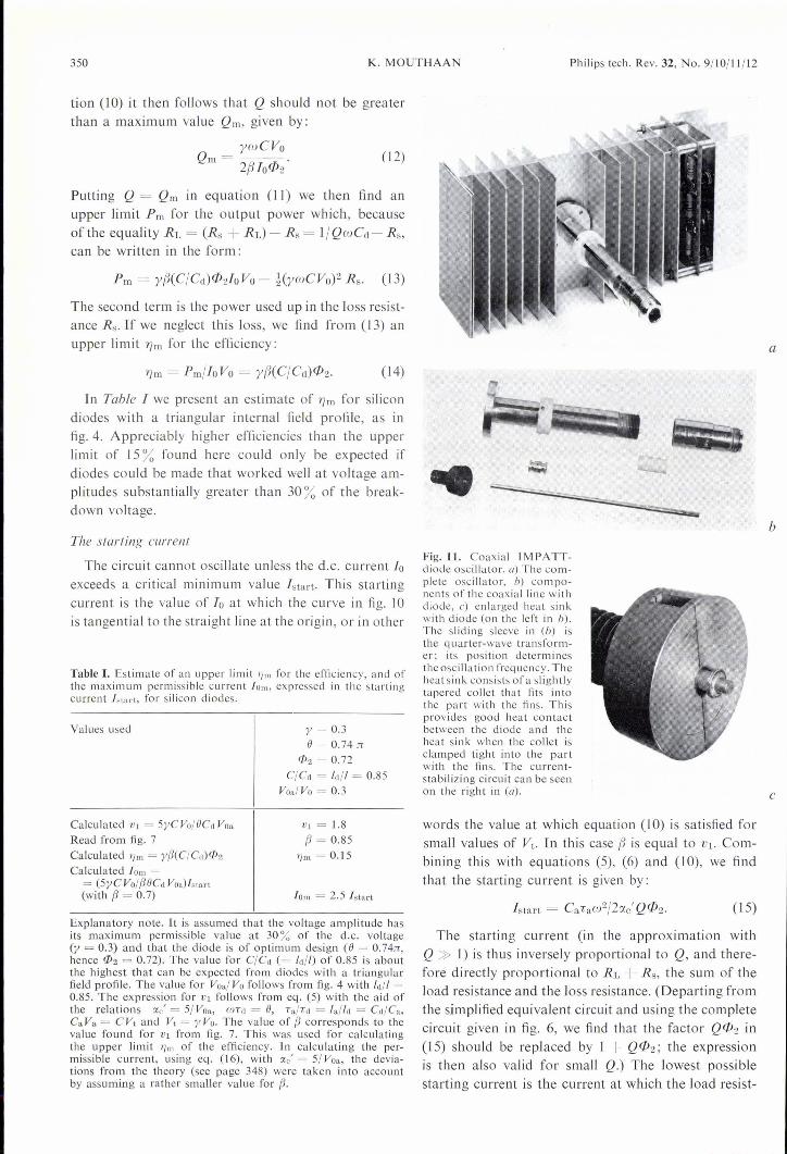
Fig.l1. Coaxial 1MPATT-diode oscillator. a) The com-plete oscillator, bJ cornpo-nents of the coaxial line withdiode, c) enlarged heat sinkwith diode (on the left in b).The sliding sleeve in (b) isthe quarter-wave transforrn-er; its position determinestheoscillation frequency. Theheatsink consists ofa slightlytapered collet that fits intothe part with the fins. Thisprovides good heat contactbetween the diode and theheat sink when the collet isclamped tight into the partwith the fins. The current-stabilizing circuit can be seenon the right in (a). C I
words the val ue at which equation (10) is satisfied forsmall values of Vt. In this case (3 is equal to VI. Com-bining this with equations (5), (6) and (10), we findthat the starting current is given by:
(15)
The starting current (in the approximation withQ» 1) is thus inversely proportional to Q, and there-fore directly proportional to RL + Rs, the sum of theload resistance and the loss resistance. (Departing fromthe simplified equivalent circuit and using the completecircuit given in fig. 6, we find that the factor Q(/j2 in(15) should be replaced by 1 + QcJJ2; the expressionis then also valid for small Q.) The lowest possiblestarting current is the current at which the load resist-
Philips tech. Rev. 32, No. 9/10/1 J / 12 IMPATI-DlODE OSCILLATORS 351
ance is equal to 0 (and Q thus equal to IlwCcIRs). Thisno-load starting current, Istart s, is a direct measureof the losses, and consequently an important param-eter of the diode and the associated oscillator circuit.In a circuit like that in fig. I the useful load resistancecan be made equal to zero - and the no-load startingcurrent thus measured - by substituting a short-ei rcuitpiston for the quarter-wave transforrner. A weaklycoupled probe is used for determining the start of theoscillation. It should be pointed out, however, that theloss resistance Rs measured in this way is not alwaysequal to the value of Rs in a circuit oscillating at ahigher level, since the losses in the diode often decreasewhen the d.c. current increases. This effect is relatedto the resistance of the "unswept region", i.e. of thenon-depleted part of the N layer (see fig. 19b of theprevious article) which is present at low currents butnot at the currents for which the diode was designed.
The requirement that the a.c. voltage should not begreater than a fraction y of the d.c. voltage is equi-valent to saying that the d.c. current in the oscillatormust not be greater than a certain factor times thestarting current. Given Vt < y Va, CaTa = CclTd andWTcl = e, we find from equation (10) and (15):
Iollstart < CC!.c'y vol c.s«Table 1 gives an estimate of the maximum permissibled.c. current calculated from equation (16). In thisestimate the deviations from theory mentioned earlier(page 348) have been taken into account by taking arather smaller value for ~ than fig. 7 would indicate.The result is that la must not be greater than about2.5 times Istart. Or, the other way round, if we wantto obtain a high output power for a given d.c. currentla, we have to ensure that Ista!"t is about 2.5 times smal-ler than la. The requirement mentioned earlier that Rsshould be much less than RL can be equated with therequirement that ISlarl s should be much less thanIStal't.
Two experimental oscillators
The coaxial oscillator of jig. 11, already mentionedin the introduction, will now be discussed in somewhatmore detail, and another type of oscillator, the micro-strip oscillator of jig. 12, will also be discussed. Bothwere designed for a freq uency of 5 G Hz and based onthe same type of diode. Some data and results ofmeasurements are presented in Table lI.
The breakdown voltage of the diode used here isj 20 V. The diode is therefore suitable for the designfrequency of 5 GHz: the product j Pi, has a value of600 V GHz, which is near the optimum value. InTable II a val ue of 0.75 has been assigned to Cl Cd;
Table Il. Data for the coaxial oscillator in fig. 11 and the micro-strip oscillator in fig. 12. Both oscillators were designed for afrequency of 5 GHz and based on the same type of diode.
Diode
Breakdown voltage Vil ~ 120 VCapacitance at breakdown e ~ 0.8 pFCl C« ~ 0.75
} measured
assumed
Coaxia I oscillator
Design values:f= 5 GHz, XL = I/wC = 40 D
Measured no-load starting current Js,"rt s = 5 mADesign value for maximum d.c. current Io,« ~ 100 mADesign value for Jst.rt ~ lom/2.5 = 40 mA (lstart » Jstart s)
Value of RL at which Js(,,·t = 40 mA, determined experimentally:RL ~ 5 D.Calculated Q = J/wCdRL = 6at [0 ~ 100 mA: measured Po = 1.1 W
calculated Po = 1.5 Wcalculated Vt = 30 V
Microstrip oscillator
Design values f = 5 GHz, X]. = I/wC = 40 n
Unloaded Jsta,t = 20 mAfound, by comparative measurement on coaxialoscillator, Rs ~ 2 n
(16)
Loaded Jstart ~ 40 mA (by adjusting coupling gap S)RI. + Rs = 5 Q (found by comparison withcoaxial oscillator)RL = 3 natlo~ 100 mA: measuredPo=0.75W
calculated, by comparisonwith coaxial oscillator,Po = ~x 1.1 = 0.66 W
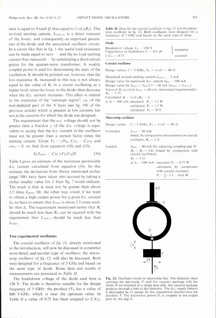
Fig. 12. Oscillator circuit in microstrip line. The dielectric sheetcarrying the microstrip [6J and the varactor package with thediode D are mounted on a single heat sink; the varactor packageprojects through a hole in the dielectric. The d.c. supply (below)is decoupled to r.f. energy by the symmetrical quarter-wave teejunction T. The microwave power Po is coupled to the outputport by the gap S.

352 K.MOUTHAAN Philips tech. Rev. 32, No. 9/10/11/12
this value is used for estimating the coaxial-oscillator Qdefined in eq. (9).
In a coaxial oscillator of the type shown in fig. I theload reactance är, is determined by the spacing betweenthe quarter-wave transformer and the diode, and theload resistance RL is determined by the diameter ofthe -inner conductor of the transformer. The completecoaxial inner conductor can be made in one piece, butin the circuit shown in fig. 11 the transformer is in theform of a sliding sleeve, which can be used to tune theoscillator.
As can be seen in fig. 11, the cooling fins account formost of the bulk of the oscillator. They are necessaryfor the rapid removal of the heat generated in the diode,which would become far too hot with no cooling; theheat developed is as much as 12 W at the voltageand current values of 120 V and 100 mA quoted inTable Il. The cooling fins are designed so that the heatsink in which the diode is mounted rises no more than15° above the temperature of the ambient air at a dis-sipated power of 15 W. To ensure good heat contactbetween diode and heat sink, the varactor package isclamped to it firmly.
From eq. (8) it follows that XL must be equal to40 Q if a frequency of 5 GHz is to be obtained withthe diode capacitance of 0.8 pF. The no-load startingcurrent Istl1l't s is measured in the way indicated above,i.e. by substituting a short-circuit piston for the quarter-wave transformer and monitoring the start of oscilla-tion by means of a weakly coupled probe. In this waya value of 5 mA was found for Istart s. To keep theheat generated within acceptable limits the maximumd.c. current was set to 100 mA. If the voltage excursionat this value is to be kept just inside the maximumpermissible value, the starting current must be 100/2.5,i.e. 40 mA. We then have Istart s« Istart, and henceRs «RL, so that only a small part of the microwavepower generated is dissipated in the loss resistance. Bytrying out quarter-wave transformers of different diam-eters, it was found that the starting current had therequired value of 40 mA when RL was equal to 5 Q.
This value of RL - at which the maximum permissiblevoltage excursion is obtained for 10 = 100 mA -could also be calculated from eq. (12) and eq. (9). Theprocedure described above for determining RL is how-ever more direct and therefore more attractive. Thetable also gives the Q associated with RL = 5 Q.
At 10 = 100 mA the factor fJ should now theoret-.ically be about 0.85 (see Table I). From eq. (10) wethen find a voltage amplitude Vt of about 30 V, i.e. 25%of the breakdown voltage. This is in fact practicallyequal to the maximum permissible voltage amplitude,as appears from the saturation of the power for anyfurther increase in the d.c. current. The output power
at 100 mA is 1.1 W (see fig. 3). Calculating the outputpower from eq. (11) with fJ = 0.85, we find 1.5 W.The difference gives some idea of the deviations fromthe theory for Vt = y Voo With a value of 0.73 for fJthe measured and calculated output power would bein agreement.
If we assume that equation (15) is valid, i.e. that thestarting current is proportional to the resistance, thenthe loss resistance Rs follows from the measured no-load starting current. With Istart s = 5 mA, andIstart = 40 mA at RL = 5 Q, we find Rs = (5/40) XX 5 R::I 0.6 Q. Since the coaxial circuit is practicallylossless, this loss resistance must be attributed almostentirely to the diode. Other direct measurements of theloss resistance have shown that at 10 = 40 mA Rs isless than 0.2 Q. This illustrates the point made earlierthat Rs often decreases as the bias current increases.
In the second oscillator to be discussed the diode isconnected to a microstrip circuit, seen from above infig. 12. The circuit consists of a thin layer of metal ona dielectric substrate [61. The varactor package contain-ing the diode D projects through a hole in the dielectricand is fixed in a metal heat sink, which also supportsthe dielectric. The actual oscillator consists ofthe diodeand the annular part of the circuit. Compared withother shapes, a ring gives low radiation losses. The d.c.is supplied from below and the microwave power isextracted at the top. The d.c. supply is decoupled fromthe microwave circuit by the symmetrical quarter-wavestub T. The oscillator is coupled to the output port viathe gap S, which also isolates the output circuit fromthe d.c. supply. Another advantage of this arrangementis that varying the coupling by varying the gap widthhas little effect on the frequency. To obtain reproducibleresults, however, the circuit should be screened. Theentire circuit is mounted in a metal box, fitted withconnectors for the d.c. supply and the output power.
In designing the oscillator the output coupling is notinitially taken into account. For reasons of symmetrythe point diametrically opposite the diode is then anopen-circuit to r.f. signals (i = 0). The left- and right-hand halves of the ring form two pieces of microstripline in parallel, which together form the terminationof the diode. After the characteristic impedance of themicrostrip line has been selected (in practice this meanschoosing the width of the strip for a given dielectricmaterial and thickness) the line lengths that will givea frequency of 5 GHz are calculated; these are the linelengths for which the reactance XL of the terminationis 40 Q (for a diode capacitance of 0.8 pF, as quotedin Table II). In the practical version an integral numberof half wavelengths are added to these lengths. Thisgave a ring circuit with an outside diameter of about4 cm for the particular dielectric used.

Philips tech. Rev. 32, No. 9/10/11/12 IMPA'IT-DIODE OSCILLATORS 353
The output strip was also omitted for the initialmeasurements on the oscillator. The starting currentwas found to be 20 mA. Comparative measurementson the coaxial oscillator showed that this correspondsto a total load resistance of 2 n, which in the presentcase is a pure loss resistance, due mainly to the circuit.These relatively high losses are attributed to the useof microstrip line.
The oscillator was then coupled to the usefulloadvia the output strip and the gap was adjusted to givea starting current of 40 mA. The gap width was deter-mined empirically, since the theoretical treatment ofthis problem is extremely complicated. The measure-ments on the coaxial oscillator indicated that the totalload resistance was then 5 n. With the measured lossresistance of 2 n, about 40% of the power generatedby the diode is lost in the microstrip circuit, leavingabout 60% as useful power. With this coupling the"maximum permissible d.c. current" is again 2.5 X 40mA, i.e. lOO mA. Considering that the diode in thecoaxial oscillator develops a power of 1.1 W at lOOmA,we therefore expect the microstrip oscillator to producea useful output of about 0.66 W. The measured outputwas 0.75 W. This result agrees well with the expectedvalue, since with the unloaded oscillator the radiatedpower at the open end was treated as a loss, whereaswith the loaded oscillator part of it appears as usefulpower.
Stability
The frequency and amplitude of the output from anoscillator should be constant (except for tuning andmodulation, of course). There should be no variations,either spontaneous or as a result of changes in the con-ditions. In an IMPATT-diode oscillator, however, low-frequency instabilities easily occur if no special atten-tion is paid to the d.c. current supply. The frequency isalso fairly sensitive to external load and temperaturevariations. These two points will now be considered.The spontaneous fluctuations that can be consideredas "noise" will be discussed in the next section.
D.e. current supply
Unsatisfactory impedance characteristics of the d.c.current supply circuit can cause instabilities in theoscillator, since the diode can behave as a device witha negative differential resistance at low frequencies aswell as at high frequencies. This is related to the wayin which the ionization coefficient a depends on thefield E (fig. 13). The steady state at breakdown is de-termined by the condition (oe) la = 1, where (oe) is thetime average of oe.Near the point (ao,Eo) on the «Ecurve where this state is reached at zero r.f. amplitude,
the second derivative of a with respect to E is positive.If an a.c. field is now superimposed on a constant fieldEo' in the vicinity of Eo, then (a) is greater than a(Eo'),and to satisfy the relation (a) la = 1 the value of Eo'must be less than Eo. This gives a decrease in the d.c.voltage across the diode with increasing amplitude ofthe r.f. voltage. Since the r.f. amplitude in an oscillatorgenerally increases with rising d.c. current, this effectgives rise to a negative differentiallow-frequency resist-
a
1J
<a>=aoJ-----------I;
a(E~) ../]00 Eo'1=-----£ '-()
k::: _::::!k::-f.:>
Fig. 13. The ionization coefficient exas a function of the field E:At high r. f. amplitudes there is a rectifying effect: the constantfield Eo' on which the r.f. field is superimposed must be smallerthan the breakdown field Eo to ensure that the relation (ex)la = 1remains satisfied.
ance which is "induced" by the r.f. voltage. We referto this resistance as Rind.
This effect is opposed by two other d.c. currenteffects, which are both equivalent to a positive differen-tial resistance. The first is a thermal effect. A variationin the d.c. current causes a variation in the heat gener-ated in the diode, and hence a variation in tempera-ture. Now, in general, the breakdown voltage increaseswith temperature. In silicon diodes with a triangularinternal field profile as in fig. 4, and at diode tempera-tures obtained in practice, this increase in Vb is about0.12 % per degree. Consequently the voltage rises whenthe d.c. current rises. The corresponding differentialresistance due to this thermal effect is referred to as Rth.Since the temperature can only follow the heat dissi-pation variations ifthey are sufficiently slow, this effectis only found at frequencies below a value known as the"thermal cut-off frequency".The second positive-resistance effect is that of the
space charge of the current-carrying electrons in the
[0) More information about microstrip line appears in thearticle "Microwave integrated circuits" by J. H. C. vanHeuven and A: G. van Nie, this issue, page 292.

354 K.MOUTHAAN Philips tech. Rev. 32, No. 9/10/11/12
drift region. This charge partly compensates the spacecharge of the donors, thus making the field gradientless steep and consequently, since the breakdown fieldis fixed, causing an increase in the voltage across thedrift region (jig. 14). If the current rises, the electronspace charge also increases; and with it the voltage.The corresponding resistance is referred to as Rsc.At Iow frequencies the diode can therefore be repre-
sented by the diagram in jig. 15. The inertia of thethermal effect is represented by the capacitance Cth,which short-circuits Rth at high frequencies.
Further analysis shows that for large signals (fJ ~ 1)the quantity Rind is about (Vt/Vo)Q times greater inabsolute value than Rsc. For Vt/Vo I::::J 0.3 the resist-ance Rind is therefore dominant when Q is greaterthan 3. Above the thermal cut-off frequency the netresistance is then negative. If Q is large enough, thiswill also be the case below the thermal cut-off frequen-cy.The instabilities caused by the induced negative resist-
ance can be countered by including in the supply cir-cuit a resistance of about 100 .Q in series with the diode.(This resistance must be bypassed by a capacitor in ther.f. circuit.) Insufficient stabilization can lead to ampli-fication ofthe low-frequency noise caused by avalanchemultiplication, and even low-frequency oscillations(e.g. in the MHz region). The result can be a seriousparasitic modulation of the r.f. signal [71.
Frequency stability; tuning
Load variations
Variations in the load lead to variations in both theoutput power and the frequency of the oscillator. In acircuit like the one shown in fig. 1 the oscillator shouldideally be terminated with a matched load, i.e. a loadwhose complex amplitude-reflection coefficient e iszero. If e is not equal to zero, power and frequencywill both differ from the ideal values. The maximumrelative deviations of power and frequency at a givene are given by:
(LJP)max/Po = 21eland
(LJW)max/W = 2Iel/QL.It depends on the argument of e whether the deviationshave the maximum value or are smaller. Equations (17)and (18) are valid if ]el -e; I, QL» 1 and I/wC § ZO.(QL = l/wCRL and Zo is the characteristic impe-dance of the coaxial line.)The relative frequency variations are a factor of QL
smaller than the relative power variations, and decreasewith increasing QL. A simple oscillator of the type infig. 1 has a QL of 10 to a maximum of 100. Greater
E
1-x
Fig. 14. The field profile in the diode, 1 for low current, 2 forhigher current. In case 2 the space charge of the donors is partlycompensated by that of the electrons in the drift region. The fieldgradient is thus smaller, and the voltage is greater than incase 1 by an amount equal to the area A. At low frequencies thiseffect corresponds to that of a positive resistance Rsc.
Fig. 15. Low-frequency equiv-alent circuit for the diode. Ifthe negative resistance Rind, in-duced by rectification of the r.f. Rlhsignal, is dominant, the circuitcan become unstable at low fre-quencies. The resistances Re«and Rth represent the space-charge effect of fig. 14 and athermal effect, and are positive.The inertia of the thermal effectis accounted for by the capac-itance Cth, which short-circuitsRth above the "thermal cut-offfrequency".
frequency stability can be obtained by coupling theoscillator to a high-Q resonant circuit. In such a casethe QL in (18) must be replaced by an effective Q forthe whole circuit. .Conversely the oscillator can be tuned by varying the
load. This principle is applied in the electronically tunedoscillator oî fig, 16. This contains a second diode, andthe voltage across this diode is kept so low that nobreakdown occurs. Variation of this voltage changesthe capacitance of the diode and hence the load on theoscillator. The oscillator can be tuned in this way overmore than 150MHz near 9.4 GHz, with no more than10% change in the power output (jig. 17).
(18) Temperature variations
(17)
To a first approximation the frequency is determinedby eq. (8). When the temperature is varied the frequen-cy therefore changes if XL and Care temperature-dependent. It follows from eq. (8) that:
1 dw 1 dC 1 dXLW dT
(19)C dT
The variation in the tuning reactance XL with tem-perature is a question of the expansion of the material

Philips tech. Rev. 32, No. 9/10/11/12 IMPATI"DIODE OSCILLATORS 355
from which the microwave circuit is made. In a circuitlike that shown in fig. 1,made from brass or aluminium,the second term in (19) gives a contribution of about-2 X10⁻⁵ K-l when the shortest possible distance ischosen between diode and transformer (approximatelyone-eighth of a wavelength); the frequency variation isgreater if this distance is made a whole number of half-wavelengths greater.
The capacitance variation depends to a great extenton whether or not the depletion layer at breakdownextends to the substrate (the N+ layer in fig. 4). If itdoes, the capacitance is virtually independent of tem-perature. If it does not, the thickness of the depletionlayer, and hence the capacitance C, varies with thebreakdown voltage Vb. In diodes with a triangularinternal field profile the relative variation of C is thenhalf that of Vb, and in the other direction. With theincrease for Vb of 0.12% per degree mentioned earlier,we thus find a contribution of +6 X 10⁻⁴ K-l for thefirst term in eq. (19). To reduce the temperature-depen-dence of the frequency diodes would thus have to bemade in which the depletion layer extended to the sub-strate. However, this is only one of the various consid-erations in choosing the thickness of the epitaxiallayer (see also the preceding article, page 340).An important source of temperature sensitivity of
the frequency does not appear from eq. (19). This canbe seen by going back from the diagram of fig. 8 to
Pa
t
Fig. 16. An electronically tuned oscillator c rcuit. A oscillatordiode. The auxiliary diode E is reverse-biased by a voltage VBbelow the breakdown value. The oscillator is tuned by varying VB.This has the effect of varying the capacitance of E, and conse-quently the terminating reactance of A and therefore the fre-quency. The oscillator can be connected to a coaxial line ormounted on the broad side of a rectangular waveguide; the innerconductor C then functions as an aerial in the waveguide.
f
I
9450MHz
9400
o 20 40-~60
Fig. 17. The frequency and the output power Po of the elec-tronically tuned oscillator of fig. 16 as a function of the controlvoltage Vn. In this measurement the d.c. supply 10 (see fig. 16)was kept at 70 mA. The dissipation in the oscillator diode A isabout one-third of the maximum permissible dissipation. (Thediode, operated here at about 9.4 GHz, had a breakdown voltageof 88 V and was thus optimized for about 7.5 GHz - illustratingthe wideband nature of the diodes, mentioned on page 348.)
that of fig. 6. The reactive current sources in fig. 6,which were later neglected, contribute to the reactivecomponent of the total current, and thus affect thefrequency. One of these sources, the one correspondingto the drift region, contains the factor (sin 8)/8. Nearthe optimum value of 8 this factor varies strongly with8 and hence with Us (see eq. 4c). It can be shownthat this makes a contribution to (I/w)dw/dT of+(1/ QL(/J2)(I/us)dus/dT. Even though this is only avariation of a correction (as is evident from the pres-ence of the factor I/QL), the effect nevertheless makesa significant contribution. Measurements show that Us
varies considerably with temperature: a value for(I/us)dus/dT of -10-3 K-l has been reported [Bl. Witha QL of 10 to 100 for a circuit like that of fig. 1 wethus arrive atacontribution of-1O-4 K-l to-1O-5K-l.Further reduction in temperature sensitivity can be ob-tained by increasing the effective value of QLby coup-ling to a high-Q resonant circuit.
[7) The effect of the rectification and of the induced negativeresistance on the noise characteristics of the oscillator areanalysed in more detail in: K. Mouthaan and H. P. M.Rijpert, Nonlinearity and noise in the avalanche transit-time oscillator, Philips Res. Repts. 26, 391-413, 1971 (No. 5),
[8) C. Y. Duh and J. L. Moll, Electron drift velocity in avalanch-ing silicon diodes, IEEE Trans. ED-14, 46-49, 1967.

356 K.MOUTHAAN Philips tech. Rev. 32, No. 9/10/11/12
NoiseThe usefulness of an oscillator depends to a very
great extent on its noise characteristics. In an IMPATT-diode oscillator operating at about the maximum per-missible amplitude these characteristics are determinedby a complicated interaction between the diode, thesupply circuit and the microwave circuit [7l. This willnot be dealt with here, but the practical significanee ofnoise will be indicated briefly, and a few experimentalresults for our coaxial oscillator will be quoted.The main applications of the oscillator will be in
telecommunications, for example in microwave radiolinks. Here the oscillator has to generate a carrier (offrequency fo) on which information can be super-imposed by amplitude or frequency modulation. If themodulation is effected by frequencies in a band B abouta central modulation frequency fm (B «fm «fo),the spectrum of the modulated carrier - neglectingnoise - will consist of a principal component at thefrequency fo, and of two components in two sidebandsof bandwidth B at the frequencies fo + fm andfo - fm. These two components contain the informa-tion, and we are therefore concerned with the noisein the two sidebands. In telephony, for instance, awidely used value for the bandwidth B is 3 kHz.
Jn amplitude modulation it is amplitude noise (ran-dom, spontaneous fluctuations in amplitude) that isof interest, and in particular the ratio PniPc. Here P«is the amplitude-noise power in the two sidebandstogether, and Pc is the power in the carrier. With thecoaxial oscillator discussed here, loaded to give a Qof about 7, a noise power of -115 dB with respect tothe carrier power was found in sidebands of 3 kHzbandwidth. Given an oscillator power of 1W the noisepower.in 3 kHz sidebands is therefore 10-12 to 10-11 W,allowing AM signals with a modulation level of 100PWto be handled. For modulation frequencies fm in therange from a few kHz to several MHz, the noise levelfound is not greatly dependent onfm. This implies thatan r.m.s. amplitude assigned to this modulation wouldbe virtually independent of fm; in other words, thenoise is virtually "white".In frequency modulation it is frequency noise that is
of interest. The level of this noise is usually expressedin an r.m.s. value Llfrms(= V(Llf2») of the instantane-ous frequency deviations LIJ This value is I/V2 timesthe amplitude of a sinusoidal frequency modulationgiving the same power (Pn) as the frequency noise insidebands of bandwidth B. From frequency-modula-tion theory the relation between Llfrmsand P« is givenby:
(Llfrmslfm)2 = PniPc.
The noise power of frequency noise, unlike that of
amplitude noise, decreases with increasingfm if Llfrmsis constant, i.e. ifthe noise is "white". With the coaxialoscillator discussed here, it was found that Llh'mswasbetween 400 and 800 Hz for a Q of 6 to 8 and 3 kHzsidebands, and that this value was practically independ-ent of fm from very low values of fm to a few MHz.This means that the oscillator would be able to handleFM signals with modulation amplitudes of a few kHz.
Improving the oscillator performance by tuning to higherharmonics
The conduction current through the diode is rich inhigher harmonics if the a.c. component of the voltageacross the avalanche layer is not too small (see fig. 5).It is possible to turn this feature to advantage [9l. Inparticular the performance of the oscillator can beimproved by tuning the circuit to one of the higherharmonics. We shall shortly discuss some of the essen-tial features of this technique. Let us confine ourselvesto a circuit which, in addition to being tuned to a par-ticular fundamental frequency, is also tuned to thesecond harmonic of that frequency. This case is rela-tively easy to realize in practice.First we shall recapitulate the situation where the
oscillator is tuned to only one frequency. The purelysinusoidal a.c. voltage across the diode then gives riseto a conduction current in the avalanche region. Theconduction current is rich in higher harmonics, and sotoo, therefore, is the total current, i.e. the sum of con-duction current and capacitive current. The externalload also determines the relation between current andvoltage. lts impedance is tuned to the correct value atthe required frequency for oscillations to occur. At allhigher harmonics, however, the impedance must bevery low, because only then can the a.c. voltage besinusoidal with a current rich in higher harmonics.We now change the external circuit in such a way
that the oscillator circuit is also tuned to the secondharmonic, while its impedance remains unchanged forthe fundamental and all other harmonics. To determinethe resultant waveform of the voltage we must knowthe relationship between the conduction current throughthe avalanche region and the voltage across it, for thecase where the voltage is no longer purely sinusoidal.If the voltage across the avalanche region differs by arelatively small amount va(t) from the average value- the value at the operating point - the conductioncurrent ia(t) through the avalanche region is given by:
/
ia(t) = ia(0)exp {k J va(r)d ..}, (20)o
where k = 2ac' I"a [lOl. This expression reveals theexponential nature of the current, which is inherent

Philips tech. Rev. 32, No. 9/10/11/12 IMPAIT-DIODE OSCILLATORS 357
Fig. 18. The conduction current i.(t) from the avalanche region (below) as given by eq. (20)for two voltage waveforms. The variation v.(t) of the voltage across the avalanche region(the solid curve in the upper figure) is a superposition of the fundamental mode (v.l) andthe second harmonic (V.2), as given by eq. (21). The two cases differ in phase <p in (21). Thevoltage amplitudes VI and V2 and the average value of the current i.(t) are the same inboth cases. The phase difference between the fundamental Fourier components (first har-monics) of current and voltage, !PI, and the phase difference between the second-harmonicFourier components !P2 - <p, are in both cases independent of Vl and V2. At <p = tt thecurrent pulses are sharper than at <p = o.
1
O~---L)~~~--------~~--~----~-t
in avalanche multiplication. It can also be seen thatthe current increases as long as Va is positive, and de-creases when Va is negative. One conclusion in partic-ular that can be drawn from eq. (20) is of interesthere: if the voltage variation is an odd function of time,vaC - t) = -va(t), then the current is an even function:iaC-t) = ia(t). This has a direct bearing on the pos-sible voltage waveform when the osciIIator is tuned toa higher harmonic.Suppose that the voltage variation and the current
are given by:
Va(t) = VI sin cot + V2 sin (2wt + cp),ia(t) = 10 + I: cos (wt + "PI) +h cos (2wt + "P2)
+ .... (21)
For oscillation to occur the phase relations betweenthe Fourier components of va(t) and fa(t) that followfrom eq. (20), the "internal phase relations", mustcorrespond to the "external phase relations", i.e. thosedetermined by the load. Before the circuit is tuned tothe second harmonic, V2 is equal to zero. In this caseva(t) is odd, so that faCt) is even, and thus containsonly cosine terms, which means that "PI (like "P2) isequal to zero. If now, as a result of tuning to 2w, aterm V2 sin (2wt + cp) of arbitrary phase cp were tobe added to va(t), then va(t) would no longer be anodd function, and from eq. (20) "PI would in general
1
be dependent on VI and V2. On the other hand, "PImust remain equal to zero, since the external impe-dance for the fundamental frequency has not changed.This difficulty is not encountered when cp = 0 or
cp = n, since in these two cases va(t) remains an oddfunction. Stable simultaneous osciIIations at the fre-quencies wand 2w can therefore occur when cp hasthe values 0 or re, and it can be proved that these arein fact the only possible values [9]. These two casesare illustrated in fig. 18.The improvement we are concerned with is obtained
at cp = n. In fig. 18 it can be seen that in this case theintervals during which the avalanche of charge carriersis built up and then broken down - i.e. the intervalsin which Va has successively a high positive and highnegative value - are shorter than when the secondharmonic is not present. Consequently the currentpulse is sharper. For a given voltage amplitude of thefundamental, this implies a greater value of fJ thanfig. 7 would indicate, and therefore, for a given d.c,current, a greater current amplitude and hence greater
[9) K. Mouthaan, Nonlinear analysis of the avalanche transit-time oscillator, IEEE Trans. ED-16, 935-945, 1969; Two-frequency operation of the avalanche transit-time oscillator,Proc. IEEE 58,510-512,1970; Nonlinear characteristics andtwo-frequency operation of the avalanche transit-time oscil-lator, Philips Res. Repts. 25, 33-67, 1970. See also note [4].
[lO) Equation (20) follows directly from equation (16) in thepreceding article on putting .is = 0, IXIa= IXcla+ IXc'va.IXcl. = 1, la = lis•• , and making ia(t) proportional to je.
358 K.MOUTHAAN Philips tech. Rev. 32, No. 9/10/11/12
power at the fundamental frequency. In the case cp = 0the current pulse is flatter and the power at the fun-damental frequency lower.
To calculate the voltage waveform that occurs at aparticular supply current, it is necessary to set up anequivalent circuit like the one in fig. 9 for both wand2w (for an accurate analysis diagrams based on fig. 6should be used). The quantities XLl, RLl, ... in thew diagram are different from XL2, RL2, ..• in the 2wdiagram. In particular we must have (see eq. 8):
XLI = I/wC,
XL2 = I/2wC.The diode is optimized to give the maximum value atthe fundamental frequency for the factor tJh in thecurrent source in fig. 9, so that ([J21 > ([J22. For eachof the frequencies the circuit has a separate Q (seeeq.9).
The current-peaking effect demonstrated in fig. 18is now taken into account by postulating that rh nolonger depends on VI alone, as in fig. 7, but also onV2 and cp. In particular, rh is greater than the valuegiven by fig. 7 if cp = 'Tt (and V2 =1= 0). Similarly f32 isaffected by the fundamental frequency, but this is ofless importance here. It follows immediately fromequations (10) and (11) that the increase in f31 corre-sponds to a greater current excursion and a higherpower at the fundamental frequency.
In normal single-frequency operation the oscillationstarts, on increasing the supply current 10, when theinitial slope of f3Ilo as a function of Va reaches acritical value (see fig. 10). This is how we found thestarting current previously (eq. 15). When f31 increasesthe initial slope of f31 also increases, so that the requiredinitial slope of f3Ilo is reached earlier and the startingcurrent is smaller. Conversely, for cp = 0, the startingcurrent is greater than with a single-frequency oscilla-tion. If we increase the supply current from low values,the first signal we obtain is therefore a two-frequencyoscillation with the phase relationship cp = st,
A significant value of V2 is only obtained providedQ2 is sufficiently large (see eq. 9), i.e. if the startingcurrent for oscillations at 2w alone, Istart 2, is suffi-ciently low (see eq. 15). In this context "sufficiently"means in practice that Istart 2 should be of the sameorder of magnitude as 10. If Rs2 is very small, it isthen possible to give Q2 a high enough value to makeIstart 2 even smaller than Istart 1. When 10 is increasedthe oscillator then starts at the higher harmonic, andthe fundamental frequency does not come in untillater.Such an oscillator can be regarded as a 2w oscillatorthat generates subharmonics. However, for this to hap-pen Q2 must be substantially greater than Ql (e.g.Q2> 100 for Ql = 7). This can be seen from eq. (15):
not only is W22 four times greater than W12, but ([J22is smaller than ([J21.
Apart from increasing the power as described above,coupling the fundamental mode to an upper harmonicmode of higher Q also gives an appreciable improve-ment in the noise characteristics of the oscillator andalso greater frequency stability.
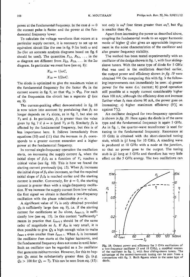
The method has been tested experimentally with anoscillator ofthe design shown in fig. 1, with four sliding-sleeve tuners. With the same type of diode for 5 GHzthat was used in the oscillators described earlier,the output power and efficiency shown infig. 19 wereobtained [111. On comparing this with fig. 3 the follow-ing improvements can immediately be seen: a) greaterpower for the same d.c.' current; b) good operationstill possible at a supply current considerably higherthan 100 mA; although the efficiency does not increasefurther when 10 rises above 90 mA, the power goes onincreasing; c) higher maximum efficiency (9% asagainst 7 %).
An oscillator designed for two-frequency operationis shown infig. 20. Here again the diode is of the sametype and the fundamental frequency is again 5 GHz.As in fig. I, the quarter-wave transformer is used fortuning to the fundamental frequency. Resonance at10 GHz is obtained with the short-circuited tuningstub, which is iJ. long for 10 GHz. A standing waveis produced at 10 GHz with a node at the junction,so that no power goes to the output. The tuningstub is iJ. long at 5 GHz and therefore has very littleeffect on the 5 GHz energy. The two oscillations can
15W 15%
1.0 10
1 0.5
20.2
100 120 140mA60 80-Ia
Fig. 19. Output power and efficiency for 5 GHz oscillations ofa two-frequency oscillator (5 and 10 GHz), a modified versionof the oscillator in fig. 1, with four sliding-sleeve tuners. Theadvantage of the second-harmonic tuning can be seen from acomparison with fig. 3. Both figures relate to the same type ofdiode.

Philips tech. Rev. 32, No. 9/10/11/12 IMPATT-DIODE OSCILLATORS 359
be accurately matched (frequency ratio I : 2) bymeans of the capacitive tuning screw, which, for5 GHz, is situated half a wavelength from the diode,i.e. electrically in parallel with it.
In this oscillator the starting current for 10 GHzoscillations varied between 35 and 45 mA from onediode to another. The starting current for 5 G Hz wasmade larger than 45 mA (45-65 mA) by choosingappropriate values for the quarter-wave transforrner.The low starting current obtained here for 10GHz (thehigh value of Q2) can easily lead to an excessive voltageexcursion at the upper harmonic. This was found togive rise to unwanted modulation by amplified low-frequency noise at output powers greater than 1 W.For output powers less than I W, however, the fre-quency noise was 20 dB less than in single-mode opera-tion.
Other possible applications of circuits operating intwo modes include amplifying frequency multipliersand frequency dividers [4l, but these will not be dealtwith here.
Injection of a stabilized signal at the second harmonic
We have seen above that it is possible, by means ofa simple rnodification to the microwave circuit, to makea two-frequency osci llator that has better characteristicsthan a single-frequency oscillator using the same diode.Achieving this in practice, however, sets a difficultspecificatien for the diode. The diode is optimized forthe fundamental frequency fo. This means that thenegative resistance at the freq uency 2fo will be corn-paratively small, so that even with relatively low inter-nal losses the diode will behave passively instead ofactively at the frequency 2fo. This disadvantage is notfound with the modified circuit shown injig. 2/, whichis therefore of practical interest.The circuit contains two IMPATT-diode oscillators
(A and B), one for the frequency fo and one for thefrequency 2/'0, each with a diode optimized for its ownfrequency. Oscillator B is stabilized by a transmissioncavity resonator C of high Q, which suppresses fre-quency noise. The signal obtained at frequency 2/'0 isinjected into oscillator A. This gives the same couplingin oscillator A between the signals of frequency fo and210 as described above. The transmission cavity resona-tor is designed so that signals of freq uency fo are nottransmitted, thus preventing oscillator A from reactingon oscillator B. The output signal from oscillator A atthe frequency fo now has the good noise characteristicsof the stabilized signal with frequency 2fo.
[11] K. Mouthaan and H. P. M. Rijpert , Second-harmonictuning of the avalanche transit-time oscillator, Proc. IEEE57,1449-1450, 1969.
Fig. 20. Coaxial oscillator circuit designed for operation attwo frequencies (5 and 10 GHz). At 5 GHz the oscillator isequivalent to the design of fig. I. A high-Q resonance at lOG Hzis obtained by means of the short-circuited stub Z which is .p.long at 10 GHz. The capacitive tuning screw S is used to matchthe two oscillations accurately in the frequency ratio I : 2.
A
(2'0)
(2fo)B
Fig. 21. Diagram for injection of a signal with double frequency.A main oscillator (frequency Io), B auxiliary oscillator (frequen-cy 2/0), C high-Q transmission cavity resonator for the frequency2/(J. The signal from B, stabilized by the cavity resonator, isinjected into A, thus improving the Q of the output signal fromA. The transmission cavity resonator only passes signals of fre-quency 2Io, not those of frequency Jó.
Fig. 22. Oscillator for 6 G Hz based on the diagram in fig. 21.The connection between the main coaxial oscillator (left) andthe auxiliary coaxial oscillator (right), including the cavity reso-nator in the middle, consists of a waveguide with a cut-off fre-quency of 8 GHz, so that 12 GHz energy is passed, but not6 GHz energy. The 6 GHz output signal contains about 30 clBless noise than that of the 6 GHz oscillator with no injected signal.
An oscillator designed on these principles has beenbuilt to operate at 6 GHz (fig. 22). The main coaxialoscillator for 6 G Hz and the auxiliary coaxial oscillatorfor 12 G Hz are connected by a piece of rectangularwaveguide. Two irises in the waveguide are arrangedto form a ~À cavity resonator at 12 GHz, with a
360 IMPATT-DIODE OSCILLATORS Philips tech. Rev. 32, No. 9/10/11/12
loaded Q of about 200. The cut-off frequency of thewaveguide is about 8 GHz, so that 12 GHz energy istransmitted, but not 6 GHz energy. The coaxial ter-minals of the 12 GHz oscillator are terminated with amatched load to avoid parasitic oscillations at lowfrequencies. The output power is taken from the coaxialterminals of the 6 GHz oscillator.With this circuit an r.m.s. frequency fluctuation of
only 10 to 20 Hz in an output signalof 1 W wasmeasured in two symmetrical sidebands of 3 kHz band-width. This is an improvement of more than 30 dB onthe 6 GHz oscillator with no injected signal.
Summary. The characteristics of IMPATT-diode oscillators areanalysed with the aid of equivalent circuits. The active element,the IMPATT diode, is reverse-biased into breakdown and sup-plied from a d.c. current source. Characteristic of the high-fre-quency behaviour are the creation of bunches of charge carriersin the avalanche region and their transit-time effect in the driftregion. Analysis gives an equivalent circuit which, at sufficientlyhigh frequencies, can be simplified to two capacitances and anr.f. current source in antiphase with the r.f. voltage. The frequen-
cy of the oscillator (diode plus termination) is primarily deter-mined by the terminating reactance, and the amplitude is deter-mined by the supply current and terminating resistance. The r.f.voltage must be limited to about 30% of the breakdown voltage.For the diodes normally used this gives an upper limit of about15% for the efficiency, and a maximum permissible supply cur-rent of about 2.5 times the starting current.
The analysis is applied to two experimental oscillators withsilicon diodes, both for 5 GHz, one in coaxial form and theother in microstrip. The output power of the coaxial oscillatoris more than 1 W, the efficiency about 7%.
Rectification of the r.f. signal in the diode can cause 10w-frequency instabilities, which must be allowed for in the designof the supply circuit. Load and temperature variations can causefrequency variations. Frequency stability is improved by coup-ling to a high-Q resonant circuit. An oscillator can be tunedby means of the load. As an example an oscillator for about9.4 GHz is discussed, which can be electronically tuned over125 MHz.The output power, efficiency, frequency and noise performance
of an IMPATT-diode oscillator can be considerably improvedby tuning the circuit to a higher harmonic. This is explainedtheoretically and demonstrated with experimental examples. Acoaxial oscillator for 5 GHz operating on these principles, andusing a silicon diode, gave an output power of 1.75 W, anefficiency of more than 9%, and a noise level 20 dB lowerthan with single-frequency tuning. A modification of this circuitthat probably offers greater practical prospects is an oscillatorcoupled to a stabilized auxiliary oscillator for the second har-monic.