Embed Size (px)
Citation preview

Antenna Array For 5g Cellular Applications
Journal of Electronics and Sensors
Research Article
Shribala N1*, Mary JS, Mounika N, Manasa P, Pragnya K Department of Electronics Communication Engineering, Bhoj Reddy Engineering College for Women, India Received: 15 March, 2020; Accepted: 17 March, 2020; Published: 20 March, 2020 *Corresponding author: Shribala N, Department of Electronics Communication Engineering , Bhoj Reddy Engineering college for Women, India . E-mail: [email protected]
Abstract
A novel low-cost, high-gain millimeter-wave antenna has been presented. The antenna is a 6 × 5 proximity-coupled planar array suitable for 5G cellular applications. Good agreement between simulated and measured results achieved shows that the proposed antenna structure is efficient in achieving broadband characteristics and low sidelobe levels with a compact size. The antenna has a gain of 21 dBi over a bandwidth of 27.5-28.5 GHz. It also exhibits an impedance bandwidth of 9.8% from 26.04 to 28.78 GHz.
Introduction Communication is a vital part of personal
life and is also important in business, education and any other situation where people encounter each other. Information dissemination, the major objective of communication is achieved by three electronic gadget (radio, television and mobile phones) known as radio systems of telecommunication. The successful design of this radio system depends on a crucial element called an antenna which is the part through which radio frequency energy is coupled from the transmitter to the outside world and in reverse to the receiver from the outside world. The recent explosion in information technology and wireless communication (such as having a bad signal when the receiver is too far from the transmitter) has created many opportunities
for enhancing the performance of existing signal transmission and processing systems.
The antenna is defined as a means of radiating or receiving radio waves. It is an arrangement of electrical conductors made to efficiently radiate and receive electromagnetic waves in desired directions. It is also considered to be an interface and a guiding structure between a transmission line and space; that is, it acts as matching systems between sources of electromagnetic energy and space. The antenna is defined as a means of radiating or receiving radio waves. It is an arrangement of electrical conductors made to efficiently radiate and receive electromagnetic waves in desired directions. It is also considered to be an interface and a guiding structure between a transmission line and space; that is, it acts as matching systems between sources of electromagnetic energy and space. All electronic communications systems consist of a transmitter,a receiver, and a communications medium. In some systems, the transmission
Journal of Electronics and Sensors 1

2
medium is a direct link such as wire, cable, or fiber-optic cable. In radio communications systems, there are no direct connections.
The system is wireless. The RF signal generated by the transmitter is sent into free space and is eventually picked up by the receiver. The processes of launching the signal into space and receiving it are the functions of the Antenna. The antenna is a device that acts as the interface between the transmitter and free space and between free space and the receiver. It converts the transmitter RF power into electromagnetic signals that can propagate over long distances, and it is also the device that picks up the electromagnetic signals and converts them into signals for the receiver. Since the antennas are typically located remotely from the transmitters and receivers, some means must be used to get power to and from the antenna. This is the job of the transmission line, a special kind of cable. An antenna is a device to transmit and/or receive electromagnetic waves. Electromagnetic waves are often referred to as radio waves. Most antennas are resonant devices, which operate efficiently over a relatively narrow frequency band. An antenna must be tuned (matched) to the same frequency band as the radio system to which it is connected, otherwise reception and/or transmission will be impaired. The gain or directivity of an antenna is the ratio of the radiation intensity in a given direction to the radiation intensity averaged over all directions. Quite often directivity and gain are used interchangeably. The difference is that directivity neglects antenna losses such as dielectric, resistance, polarization, and VSWR losses. Since these losses in most classes of antennas are usually quite small, the directivity and gain will be approximately equal (disregarding unwanted pattern characteristics). Real antennas are different, however, and do not have an ideal radiation distribution. Energy varies with angular displacement and losses occur due to side lobes. However, if we can measure the pattern, and determine the beam width we can use two (or more) ideal antenna models to approximate a real antenna pattern Assuming the antenna pattern is uniform, the gain is equal to the area of the isotropic
sphere (4Br2) divided by the sector (cross section) area. G = Area of Sphere / Area of Antenna pattern An antenna is an electrical conductor or system of conductors Transmitter Radiates electromagnetic energy into space Receiver Collects electromagnetic energy from space. In comparison to 4G networks, the millimeter wave 5G network offers a very significant advantage in network performance due to the much wider RF bandwidth it utilizes. It promises great features like increased data rates of several tens of megabits per second for tens of thousands of users, greatly enhanced spectral efficiency, improved coverage, relay technologies to reduce power consumption, and much more. Moving to the mmWave frequencies for 5G mobile terminals requires new techniques in the design of antennas for mobile-station (MS) and base-station (BS) systems in order to overcome the issue of high path loss associated with higher frequencies. Due to this, microstrip patch array antennas and phased arrays are widely studied as possible candidates for mmWave applications with features such as high gain, beam steerable radiation patterns and low profiles. One way to achieve an efficient beam-steerable phased array antenna, which is one of the most important blocks for 5G cellular systems, is by creating planar arrays by the assembly of smaller linear arrays. Increasing the number of linear arrays increases the gain and forms pencil beams to extend coverage ranges significantly and compensate for signal degradation due to high path loss.Microstrip patch antennas with direct-feed structures generally have very compact sizes but tend to possess narrow bandwidths (1-5%). Coupled feeding structures such as proximity and aperture coupled antennas typically have higher bandwidths (5-30%) but are bigger than direct-feed antennas due to their corporate- feed networks. Corporate-feed networks have bandwidth enhancing capabilities but require more space as the number of patch elements increases. Figure (1): Structure of subarray antenna.

3
The extra space is used to accommodate power dividers, transformers and meandered lines to make the corporate division possible. This increases losses and design complexities. Symmetry in corporate networks is also mostly desired as 2n (even) x 2n (even) planar arrays are easier to form than 2n (even) x 2n – 1 (odd) and 2n - 1 (odd) x 2n – 1 (odd) arrays which prove to be quite complex in power division. Literature shows that 5G coupled- feed type planar microstrip antennas are uncommon with one of the reasons being the cumbersome nature of the corporate-feed network associated with them. On the other hand, 5G direct-feed planar arrays are more common and even though they have narrower bandwidths, they are much simpler to design and are more compact while possessing similar gain characteristics (20- 25 dBi). Therefore, when wider bandwidths in mmWave applications are required, literature shows that substrate integrated waveguides, leaky wave antennas and other types of antennas are preferred to proximity coupled and aperture coupled antennas. In, a novel linear structure is proposed which has both the bandwidth capabilities of a coupled antenna and a series configuration as that of a direct-feed antenna. The antenna is shown in Fig. 1. It has a simple structure which permits the easy formation of tightly spaced planar and phased arrays with a coupled-feed structure which in general is quite difficult to design. In this paper, a 6 x 5 array is formed to verify the simplicity of the planar array formation capabilities of the antenna in [12] while achieving a gain higher than 21 dBi with a beamwidth of 15o and sidelobe levels below -18 dB in both planes at 28 GHz. The proposed planar array has a bandwidth of 9.8% and demonstrates a way of forming
proximity coupled microstrip planar arrays without the use of cumbersome corporate feeding. Figure (2): Radiation characteristics of varied element patch width Pw.
networks with the ability to easily form any planar configuration desired. This can also be extended for aperture coupled structures as well. Recently, ultra wideband technology has received great attention in various fields for the short range, low power consumption, compactness, low-cost, excellent immunity to multipath interference and reduced hardware complexity. The Federal Communications Commission (FCC) of the United State officially released the regulation for Ultra wideband (UWB) technology. In this regulation, the spectrum from 3.1 GHz to 10.6 GHz is allocated to the unlicensed indoor UWB communication systems. Therefore, one of the main issues in UWB communication system is the design of a compact antenna which provides wideband characteristics over the whole UWB range of frequencies. One of the major design considerations of a practical UWB antenna is the co-existence with existing narrowband communication systems. For instance, the 5- GHz band wireless local area network (WLAN) operates at the band. Based on the above requirements, many antenna configurations including planar monopole, dipole and slot antenna have been developed so far. In these antennas, a variety of shapes and bandwidth enhancement techniques has been studied. Several shapes such as diamond, ring, bow-tie, elliptical and square shapes have been proposed to satisfy UWB specifications. In these antennas, several bandwidth enhancement techniques are used to have a continuous UWB bandwidth. Many

4
CPW-fed slot antenna configurations have also been proposed and developed. It includes wide rectangular slot, a bow-tie slot and some other broadband designs such as using a patch element loaded in a circular slot and a diamond patch in a rectangular slot. To achieve frequency rejected characteristic, different techniques are used including an embedded inverted U-shape, an embedded two slit on a circular monopole, adjusting a V-shaped thin slot length on the bow-tie shape slot antenna and an embedded U-shape on a beveling rectangular patch. A compact CPW-fed ultra-wideband antenna with band notched characteristic has also been studied. In this study, a tuning stub is inserted in the middle of the fork-like patch to achieve the band rejection characteristic. Another compact antenna study has a C- shaped slot to obtain the band-rejection operation of the antenna . A slot-type split- ring resonator (STSRR) is inserted into the center line of the CPW to notch the wireless local area network (WLAN) frequency band. Nowadays, it is often required to design an antenna which can be used for multifunctional systems such as 2.4 GHz and UWB systems. General Description An antenna is a device to transmit and/or receive electromagnetic waves. Electromagnetic waves are often referred to as radio waves. Most antennas are resonant devices, which operate efficiently over a relatively narrow frequency band. An antenna must be tuned (matched) to the same frequency band as the radio system to which it is connected, otherwise reception and/or transmission will be impaired. The gain or directivity of an antenna is the ratio of the radiation intensity in a given direction to the radiation intensity averaged over all directions. Quite often directivity and gain are used interchangeably. The difference is that directivity neglects antenna losses such as dielectric, resistance, polarization, and VSWR losses. Since these losses in most classes of antennas are usually quite small, the directivity and gain will be approximately
equal (disregarding unwanted pattern characteristics). Real antennas are different, however, and do not have an ideal radiation distribution. Energy varies with angular displacement and losses occur due to side lobes. However, if we can measure the pattern, and determine the beam width we can use two (or more) ideal antenna models to approximate a real antenna pattern Assuming the antenna pattern is uniform, the gain is equal to the area of the isotropic sphere (4Br2) divided by the sector (cross section) area. G = Area of Sphere / Area of Antenna pattern An antenna is an electrical conductor or system of conductors Transmitter - Radiates electromagnetic energy into space Receiver - Collects electromagnetic energy from space. The IEEE definition of an antenna as given by Stutzman and Thiele is, “That part of a transmitting or receiving system that is designed to radiate or receive electromagnetic waves”. Horn antenna is the most important part of communication system because it is widely used antenna at UHF frequency and microwave frequency. It is a type of aperture antenna used for various applications. Horn antenna is used as a feed element in large antennas. It is also used as a standard antenna to compare it with other antennas. In this paper various techniques have been studied to design a horn antenna and to improve its gain. There are a number of materials used for designing a horn antenna, one of them is carbon based composite materials. The waveguide slot antenna arrays are the most attractive candidates for the high- gain wideband planar antennas for many applications. They suffer neither from dielectric nor radiation loss and are suitable for applications requiring high gain and high efficiency. However, wideband waveguide slot arrays require corporate feed networks that become very complex and bulky. In addition, at high frequencies, such feed networks require accurate, high precision and expensive manufacturing. In particular it is difficult to provide good electrical contact between different metal layers of the construction. Apart from the problem of

5
metal contact, the antennas need very thin slot layer (100-200μm) which raises mechanical challenges during assembly due to bending of these very thin slot layers. Applications requiring high gain antenna such as the parabolic reflector can be applied with the horn antenna to enhance the higher gain. Rectangular horn has been used for microwave antenna a long time. Its gain can be increased by enlarging the construction of horn to flare exponentially. Types of Antenna Rectangular Horn Antenna Horn antennas are popular in the microwave bands (above 1 GHz).Horns provide high gain, low VSWR (with waveguide feeds), relatively wide bandwidth, and they are not difficult to make. There are three basic types of rectangular horns Shown in (Figure 3). Figure( 3): Various horn antenna systems
The horns can be also flared exponentially. This provides better impedance match in a broader frequency band. Such horns are more difficult to make, which means higher cost. The rectangular horns are ideally suited for rectangular waveguide feeds. The horn acts as a gradual transition from a waveguide mode to a free- space mode of the EM wave. When the feed is a cylindrical waveguide, the antenna is usually a conical horn. Conical Horn Antenna Another very practical microwave antenna is the conical horn, the feed of a conical horn is often a circular waveguide. The conical horn antenna has a circular cross section and is seen less frequently than the rectangular. The Conical Horn
Antenna was designed by using a soft HFSS software with circular waveguide dimensions of waveguide diameter a=20cm and waveguide length L=20cm, Horn dimensions of Horn radius a‟= 28cm and horn Flare Length FL=40cm and wall thickness t=0.4cm. The geometrical 3D view of designed Conical Horn Antenna in HFSS the conical horn antenna was designed Shown in (Figure 4) Figure ( 4): Conical horn antenna
The conical horn antenna was designed. Its parameters, specifically the length and the output radius, were optimized for minimal level of entire side lobes and maximum of directivity in the main direction. The initial horn has directivity about 20 dB. The diameters reached from the optimization are the length of 182 mm and the radius of 76 mm. Flat Scalar Ring Horn Antenna Scalar ring is one type of horn antenna system and the concentric metallic rings on a scalar-ring 0deflect the signals arriving at sharp angles (from the fringes of the dish, outside the dish etc.,) away from the mouth of the feedhorn. Signals arriving at sharp angles are mostly bad, and contribute to noise.The Flat Scalar Ring Horn Antenna was also designed by using advance EM simulation software Ansoft HFSS with circular waveguide antenna performance in terms of polarization, small size, light weight and multi path rejection are observed. The three different types of horn antennas are simulated with commercially available software known as Ansoft HFSS (High Frequency Structure Simulator), detailed design procedure with dimensions are presented and performance results are measured.The proposed antenna gives decent gain over operating range of L and S
6
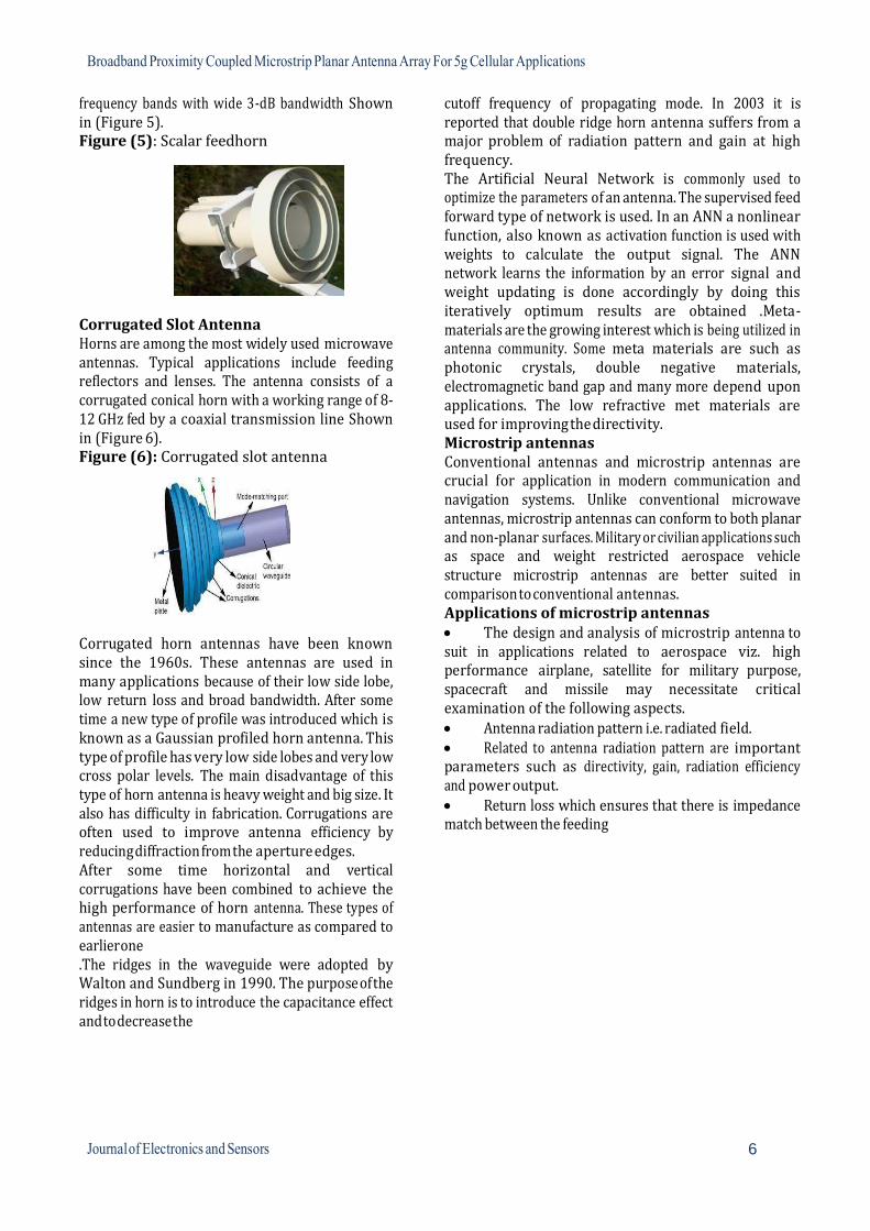
frequency bands with wide 3-dB bandwidth Shown in (Figure 5). Figure (5): Scalar feed horn
Corrugated Slot Antenna Horns are among the most widely used microwave antennas. Typical applications include feeding reflectors and lenses. The antenna consists of a corrugated conical horn with a working range of 8-12 GHz fed by a coaxial transmission line Shown in (Figure 6). Figure (6): Corrugated slot antenna
Corrugated horn antennas have been known since the 1960s. These antennas are used in many applications because of their low side lobe, low return loss and broad bandwidth. After some time a new type of profile was introduced which is known as a Gaussian profiled horn antenna. This type of profile has very low side lobes and very low cross polar levels. The main disadvantage of this type of horn antenna is heavy weight and big size. It also has difficulty in fabrication. Corrugations are often used to improve antenna efficiency by reducing diffraction from the aperture edges. After some time horizontal and vertical corrugations have been combined to achieve the high performance of horn antenna. These types of antennas are easier to manufacture as compared to earlier one .The ridges in the waveguide were adopted by Walton and Sundberg in 1990. The purpose of the ridges in horn is to introduce the capacitance effect and to decrease the
cutoff frequency of propagating mode. In 2003 it is reported that double ridge horn antenna suffers from a major problem of radiation pattern and gain at high frequency. The Artificial Neural Network is commonly used to optimize the parameters of an antenna. The supervised feed forward type of network is used. In an ANN a nonlinear function, also known as activation function is used with weights to calculate the output signal. The ANN network learns the information by an error signal and weight updating is done accordingly by doing this iteratively optimum results are obtained .Meta- materials are the growing interest which is being utilized in antenna community. Some meta materials are such as photonic crystals, double negative materials, electromagnetic band gap and many more depend upon applications. The low refractive met materials are used for improving the directivity. Microstrip antennas Conventional antennas and microstrip antennas are crucial for application in modern communication and navigation systems. Unlike conventional microwave antennas, microstrip antennas can conform to both planar and non-planar surfaces. Military or civilian applications such as space and weight restricted aerospace vehicle structure microstrip antennas are better suited in comparison to conventional antennas. Applications of microstrip antennas The design and analysis of microstrip antenna to suit in applications related to aerospace viz. high performance airplane, satellite for military purpose, spacecraft and missile may necessitate critical examination of the following aspects. Antenna radiation pattern i.e. radiated field. Related to antenna radiation pattern are important parameters such as directivity, gain, radiation efficiency and power output. Return loss which ensures that there is impedance match between the feeding

7
network and the microstrip patch antenna. Pattern and impedance bandwidth. Low impedance bandwidth results due to use of thin dielectric substrate, alternatively use thick dielectric but it will enhance surface wave and deteriorate radiation pattern and efficiency. Advantages and limitations of microstrip antennas It is worth mentioning the advantages as well as the limitations of microstrip antennas. Well known facts which highlight the microstrip antenna as compared to conventional microwave antenna are: Because of its size, light weight, ease of installation and thin profile configurations it can be made conformal. Integration with microwave integrated circuits is relatively easier. It is versatile as far as resonance frequency, polarization, radiation pattern and impedance bandwidth is concerned.
Along with the microstrip antennas structure, associated feed lines and matching network can be simultaneously fabricated.
Can be made mechanically robust when conformed on rigid surfaces.
antenna as compared to conventional antenna are:
High Q resulting in narrow bandwidth, generally a few percent.
Low gain and efficiency, in addition to high
levels of cross polarization.
watts.
Thicker substrate results in excitation of surface waves.
space. Why microstrip antennas Despite the above stated limitations of the microstrip antennas, it is these properties of low profile, light in weight, conformable to both planar and non planar
structure, easy to fabricate and integration to MIC that makes it superior to conventional flush mounted antennas. Hence in practice, microstrip antennas are extensively used in several applications meet the challenging system requirement due to the above stated facts. In addition effort to develop microstrip antennas configuration with accurate and rugged analytical model needs understanding of its limitations as well as improve design and optimize its performance. Microstrip antenna arrays Single microstrip patch antenna may not be suitable for application, which needs high gain, beam scanning or enhance bandwidth. In order to enhance gain and to achieve beam steering capability the arrays formation of microwave antenna is resorted to. The same concept of array formation may therefore be used with the microstrip patch antenna as well. Antenna arrays may be linear, planar or conformal. In applications related to radar and communication systems narrow beam is desired and hence planar array configuration may be used for such a requirement. Microstrip planar arrays Considering that edge effects are subjected to all the elements, the design of finite arrays necessitates grouping of the patches in a symmetrical pattern so that radiation in the desired direction is obtained. This can be achieved only when fields due to individual patches get combined in phase in the desired direction and cancel each other in all other directions. In other words each patch output is combined to obtain the fields radiated by the array. It is important to note that radiation pattern of individual patch in the array is the same when it is in stand- alone mode. Hence the original pattern of the individual patch gets multiplied by the array factor that takes into consideration the amplitudes and phases of the feed current. However due to closer proximity between patches in the array there is interaction between the elements. Since each patch element induces currents to the other adjacent patches, it leads to coupling among the radiating patches. 1.6 Antenna parameters:

8
Bandwidth The bandwidth of an antenna is defined as "the range of frequencies within which the performance of the antenna, with respect to some characteristic, conforms to a specified standard." The bandwidth can be considered to be the range of frequencies, on either side of a center frequency, where the antenna characteristics such as input impedance, pattern, beam width, polarization, side lobe level, gain, beam direction, radiation efficiency are within an acceptable value of those at the center frequency Bandwidth can be defined in terms of radiation patterns VSWR/reflected power. Percentage bandwidth is defined as: FH is the highest frequency in the band FH – FL/ FC FL is the lowest frequency in the band FC = FH + FL/2 FC is the center frequency of the Center. Impedance matching For efficient transfer of energy, the impedance of the radio, the antenna and the transmission line connecting the radio to the antenna must be the same. Radios typically are designed for 50 Ohms impedance, and the coaxial cables (transmission lines) used with them also have 50 Ohms impedance. Efficient antenna configurations often have impedance other than 50 Ohms. Some sort of impedance matching circuit is then required to transform the antenna impedance to 50 Ohms. Input impedance The input impedance of an antenna is defined as “the impedance presented by an antenna at its terminals or the ratio of the voltage to the current at the pair of terminals or the ratio of the appropriate components of the electric to magnetic fields at a point”. The power associated with the radiation resistance is the power actually radiated by the antenna, while the power dissipated in the loss resistance is lost as heat in the antenna itself due to dielectric or conducting losses. Return loss
It is a parameter which indicates the amount of power that is “lost” to the load and does not return as a reflection. Hence a parameter to indicate how well the matching between the transmitter and antenna has taken place. The bandwidth can be calculated from the return loss (RL) plot. Vswr (voltage standing wave ratio) Voltage Standing Wave Ratio (VSWR) is an indication of the quality of the impedance match. VSWR is often abbreviated as SWR. A high VSWR is an indication the signal is reflected prior to being radiated by the antenna. VSWR and reflected power are different ways of measuring and expressing the same thing. When the condition of matching is not satisfied, that means, ZL = Z0, then the power may be reflected back which leads to the creation of standing waves. The standing waves can be characterized by a parameter called Voltage Standing Wave Ratio (VSWR). The VSWR expresses the degree of match between the transmission line and the antenna. When the VSWR is 1:1, the match is perfect and all energy is transferred to the antenna prior to be radiated. In addition, for an antenna to be reasonably functional, a maximum value of VSWR. Radiation pattern For a linearly polarized antenna, performance is often described in terms of its Principal E- and H-plane patterns. The E- plane is defined as "the plane containing the electric-field vector and the direction of the maximum radiation." The H-plane as "the plane containing the magnetic field vector and the direction of the maximum radiation."The radiation pattern of an antenna is a plot of the far-field radiation properties of an antenna as a function of the spatial co-ordinates which are specified by the elevation angle (θ) and the azimuth angle (φ). Because this parameter was so important to our software simulations we needed to understand it completely. More specifically it is a plot of the power radiated from an antenna per unit solid angle which is nothing but the radiation intensity.
9
It is an extremely parameter as it shows the antenna’s directivity as well as gain at various points in space. It serves as the signature of an antenna and one look at it is often enough to realize the antenna that produced it. Radiation or antenna pattern describes the relative strength of the radiated field in various directions from the antenna at a constant distance. The radiation pattern is a “reception pattern” as well, since it also describes the receiving properties of the antenna. The radiation pattern is three-dimensional, but it is difficult to display the three- dimensional radiation pattern in a meaningful manner. Radiation pattern lobes Various parts of a radiation pattern are referred to as lobes, which may be sub classified into major or main, minor, side, and back lobes. A radiation lobe is a "portion of the radiation pattern bounded by regions of relatively weak radiation intensity." A major lobe is defined as "the radiation lobe containing the direction of maximum radiation." A minor lobe is any lobe except a major lobe. A side lobe is "a radiation lobe in any direction other than the intended lobe. These pattern measurements are presented in either a rectangular or a polar format.It is also time- consuming to measure a three-dimensional radiation pattern. Often radiation patterns measured are a slice of the three- dimensional pattern, resulting in a two- dimensional radiation pattern which can be displayed easily on a screen or piece of paper. Efficiency Antenna radiation efficiency is defined as the ratio of power radiated to the input power. It relates the gain and directivity. Radiation efficiency also takes into account conduction and dielectric losses. Project overview In patch antennas, characteristics such as high gain, beam scanning, or steering capability are possible only when discrete patch elements are combined to form arrays. The elements of an array may be spatially distributed to form a linear, planar, or volume array. Planar arrays have elements
distributed on a plane. Planar array configurations are extensively used in both communication and radar systems where a narrow pencil beam is required. Individual elements can be positioned along a rectangular grid to form a planar array for better control of beam shape and position in space. Planar arrays of printed radiating elements are potentially good candidates for low cost scanning array applications. Microstrip patch arrays are versatile as they can be used to synthesize a required pattern that cannot be achieved with a single element. In addition, they are used to increase the directivity and perform various other functions, which would be difficult with any one single element. Configurations of a 6×5 patch array have been analyzed and an optimum frequency range of the patch antenna array has been arrived at. It is inferred that for any planar array configuration, optimized antenna characteristics can be obtained, depending upon element spacing. The effects of surface waves and mutual coupling can be minimized by optimizing the inter element spacing in both the planes. The antenna provides frequency close to the designed operating frequency with an acceptable Directivity and Gain. When antenna structure is closely spaced, the return loss improves in the E plane. It has been shown that with the increasing array spacing, the gain of the antenna gets reduced significantly. Microstrip Patch Antenna This chapter discusses about the concept of the Microstrip patch i.e, we present their designs, problems solved, advantages and limitations. Structure of Microstrip patch antennas There is growing interest in planar antennas that are easily integrable with other RF and microwave circuits. However, using planar antennas for pico-satellite communications has many challenges in terms of gain, bandwidth and antenna size; specifically those outlined in (Table 2.2). In the sequel, we present their designs, problems solved, advantages and limitations. (Figure 7) shows a typical microstrip patch antenna that consists of a metal (`Patch') on the top of a grounded dielectric

10
substrate. This patch can be made of different shapes; rectangular being the most common shape. Moreover, the patch antenna is fed by a microstrip transmission line. The patch and feed line are usually made from copper. Patch antennas have been used Figure( 7): A microstrip patch antenna.
for different applications. They include medical [55], [56], CubeSat; i.e., earth observation [30], and military applications, i.e., elements array in radar scanning [55]. To date, we have identified eighteen designs aimed at microstrip patch antennas with the goal of achieving beam steerability, increasing gain, reducing their size, and enhancing supported bandwidth. As Table2.1 shows, all these designs achieve gains ranging from 1.53 to 18 dB, with an antenna size ranging from 3:14×0:82×0:078 cm3 to 12×16:8×2:5cm3. Moreover, they work in the L, S, C and X frequency bands (1 × 14.15 GHz). In terms of gain and size, most of these designs are suitable for pico-satellites communications. Amongst all microstrip patch antenna designs we report later, i.e., those in the one in has the highest gain at 18 dB and operates in the 6.175 GHz. However, its size, i.e., 16 × 16 × 0:35cm3, rules it out for use by pico- satellites. On the other hand, the design in has the smallest dimension at 2:7×2:7×0:0892 cm3 and a high gain of about 6 dB. In terms of operating frequency, all the designs are suitable for satellite links and wireless communication applications as they operate in the super high frequency (SHF) band (2-30 GHz). However, the most suitable frequency band for pico-satellites is the S- band (2-4 GHz). Moreover, one limitation of the antenna designs is the lack of steerability.
This is very important for cross links, and secure communications. We will further discuss these proposals in more details in terms of their gain and steerability and we present antennas that have high bandwidth while the other presents those that are size sensitive. Steerability and gain improvement Recently, beam-steerable and high gain antennas have received considerable attention due to their enhanced radiation performance and suitability for long distance communications. The main techniques used to achieve beam steering include sequential phase-rotation, retro directive array [45], beam forming algorithm [40], and for increasing gain, photonic band-gap (PBG) structures [50], and single proximity coupled feed [42].We note that conventional pointing mechanisms, such as [47], for steering antenna beams are not suitable for use by pico-satellites because of their size and mass constraints.

11
Broadband Proximity Coupled Microstrip Planar Antenna Array For 5g Cellular Applications Table 1: Different microstrip patch antenna designs and their performance

12
Sequential Phase-Rotation Sequential phase-rotation is a popular approach. The main idea is to feed each sub-array element sequentially by making adjacent patches orthogonally oriented (90˚) to achieve CP at the following phases: 0˚, 90˚, 180˚, and 270˚. In [47], Osorio et al. propose a square antenna array with nine identical elements (3 × 3). Each element is formed by a 2 × 2 sub-array of rectangular patches. Adjacent patches are orthogonally oriented to provide CP. Beam steerability is achieved by feeding the sub-arrays at 0˚, 90˚, 180˚, and 270˚ using a phase shifter. They reported beam steerability and a high gain of 6.9 dB. The use of rectangular patches leads to a reduction in mutual coupling between adjacent patches. This improves performance due to the isolation between antenna arrays. This also leads to a reduction in interference between array elements. Its main limitation, however, is the low coupling between the feed line and the radiating patch. This significantly affects impedance matching and radiating efficiency. To solve this problem, Osorio et al. propose moving the feed line slot back to the centre of the patch where the coupling through the electrical dipole is maximized. Another limitation is its inability to switch between two different polarizations, which is an important feature as it helps enhance the reception of weak signals. Microstrip arrays can provide various radiation characteristics with their feed networks, which are often designed using power dividers (or a combiner) to deliver a RF signal with specific amplitude and phase to each radiating element. In [44], Ma et al. propose a technique to achieve polarization diversity and an electrically steerable radiation pattern. The main approach is a three quasi-lumped couplers and a 90˚ phase delay line. The operation of these couplers can be switched between the T-junction divider mode and 3-dB hybrid mode by controlling the capacitance value of the lumped capacitors. By connecting this feed network to four rectangular radiating elements of the microstrip array, the T-junction divider provides linear polarization while a 3-dB
hybrid provides CP. This is important as it achieves the best signal strength and mitigates multipath fading. Moreover, the beam steering capability of circular polarization allows a link to be established when re-orienting two satellites. It is interesting to note that steerability and high gains of 7.1dB and 7.5 dB are obtained for CP and LP respectively. One major drawback is the antenna size, i.e., 15×15×0:96cm3, which exceeds the size of pico-satellites. Power dividers, which distribute power to different radiating elements, facilitate beam steering control. In [49], Hu et al. use a two-way Wilkinson power divider [64] to feed a network array that has sequential rotated elements. This power divider provides high isolation and 90˚ phase shift between adjacent radiating elements and sub-arrays. This is important as it achieves broadband CP at high gains. They reported beam steerability, wide bandwidth and a superior gain of 18 dB. This design achieves wider bandwidth and much higher gain than the designs presented in [44] and [47]. Compared to [44], which uses a three-port power divider, the two-way divider in [49] occupies a smaller area because it reduces the total size of the feeding network layout. Its main limitation is the large antenna size (16cm×16cm×0:35cm). This has a non- negligible impact on the actual surface area used for solar cells, and hence energy harvesting rate, which in turn affects operational lifetime. Another limitation is the use of a 90_ phase shifter, which has a significant impact on cost, dimension and is complex to control. One of the most popular power divider designs is the Wilkinson power divider [65]. It splits the input power signal into n signals of equal amplitude and phase, and is commonly applied in antenna array systems that require corporate or parallel feed systems. In [30], Nascetti et al. used a Wilkinson structure to design a power divider that feeds a network array of four identical patches placed on 1U CubeSat face. This power divider design provides a high isolation between the output ports at good impedance matching. The main idea is to feed every two adjacent patches that are

13
orthogonally oriented (90˚) using a power divider to achieve CP at high gain. This is important as it increases the reception and signal strength; it thus helps establish communication links with a ground station and other CubeSats. The design achieves a maximum gain of 5.9 dB and a return loss of -15.05 dB at an operating frequency of 2.45 GHz for a single patch. Moreover, the authors used all four patches to achieve a high gain of 7.3 dB and a small return loss of -25 dB at 2.45 GHz. Compared to the designs in [44], [47], and [49], the one reported in [30] has a much smaller antenna size, i.e., 3:97 × 1:2 × 0:21cm3, and less complex. However, its main limitation is the implementation of the antenna design on only one face of the CubeSat. This means directivity is maximized in one direction, meaning no cross-links communications when CubeSats are oriented toward a ground station. Retro directive (Self-Steering) Approaches that use retro directive arrays [66]-[68] are becoming popular due to their simplicity as compared to those that use phased-arrayand smart antennas.Specifically, retrodirective antennas are able to reflect an incident signal towards the source direction without any prior location information. In [45], Mizuno et al. use a retrodirective (self- steering) array. This technique is an alternative to dynamic beam steering and also helps increase gain. We note that conventional phased- array antennas use phase shifters to achieve beam steerability. In contrast, retrodirective arrays steer their beams by sensing the incoming signal without the need for phase shifters. Consequently, they are cheaper, less complex, lighter, and smaller in size. Compared to smart antennas that rely on digital signal processing for beam control, e.g., [44], [47], [49], retrodirective array systems are much simpler and potentially faster because it does not require computation. However, its main limitation is the use of a high local frequency that is set to twice the incoming radio frequency. Hence, this incurs high power, which is a key limitation of pico-satellites due to their scarce energy resource.
Beam Forming Algorithm Approach Different antenna array systems use beam forming algorithms to control radiation patterns. Budianu et al. [40] propose to install a micro-strip patch antenna on each face of cube satellites. Each antenna provides CP. A beam forming algorithm is then used to identify a spatial signal signature. This is important as it maximizes directivity for any link direction. Also, the use of six antennas ensures a communication link remains available at all times regardless of CubeSats orientation. Compared to the designs in [44], [47], and [49] that use complex digital signal processing and a phase shifter to steer beams, beam forming algorithms are more simple as they are based on simply adding the electrical fields of adjacent antennas, and hence, have a high gain. However, this approach occupies precious space that otherwise could be used for solar cells. Photonic Band-Gap (Pbg) Structures Surface-wave losses in patch antennas lead to a decrease in radiation efficiency and gain. Therefore, surface-wave suppression techniques are needed to enhance radiation pattern efficiency. Most of these techniques are related to periodic structures [69]-[73]. The most popular one are Photonic band-gap (PBG) structures [74]. In [50], Qian et al. propose to surround a patch antenna with a square-lattice of small metal pads. This leads to a substantial suppression of surface waves excited in the dielectric substrate. They reported a radiation efficiency of 85% and a gain of 5.02 dB. In general, this technique achieves wider bandwidth, higher gain, lower backside radiation, beam shape control and surface wave suppression. Unfortunately, the resulting antenna is not steerable. Single Proximity Coupled Feed A proximity coupled feed technique is used to transfer power between the microstrip line and the radiating patch based on electromagnetic field coupling [75]. In [42], Iwasaki presents a design for a circularly polarized patch antenna with a single proximity couple feed line. This antenna has a cross slot with unequal lengths on its patch. A single

14
proximity coupled feed is an electromagnetically coupled method. This electromagnetic field coupling is carried out to transfer power between the microstrip line and the radiating patch. This leads to higher isolation between the DC supply and RF signal. It achieves a CP without the need for an external circular polarizer. This is important as it is less complex and incurs less weight and size. Iwasaki reported a high gain of 6 dB at CP which is important for cross- link communications in picosatellites. Another advantage is the ability to control gain, resonant frequency and antenna size. Antenna bandwidth enhancement The main techniques used to enhance bandwidth include agile polarization [24], cavity [41], U-slot and L-slit geometries [23], folded-patch approach [28], and transparent mesh line geometry [51]. All these techniques achieve significant enhancement in bandwidth ranging from 3.8% in the 3.8 GHz frequency band to 98.22% in bands ranging from 4 to 11 GHz. Moreover, these approaches have no significant effect on antenna size. Agile Polarization Antennas of this type are able to dynamically change their polarization state, i.e., they can have either linear (vertical or horizontal) or CP (left or right hand) .Ferrero et al. designed a novel quad-polarization agile patch antenna to achieve simple polarization reconfigurability and to enhance bandwidth. The main approach is to feed a radiating patch with two orthogonal slots that are excited by a tunable quasi-lumped coupler (QLC). These couples can be switched between two different operating modes: 3-dB hybrid coupler and directional coupler via a DC bias voltage to achieve agile polarization capabilities. This is important as it addresses multipath fading. The resulting antenna has a wide 3 dB axial ratio CP bandwidth of 3.8% with respect to the centre frequency of 3.5 GHz. Cavity Model This technique is used to analyze microstrip patch geometry and to provide a better way to model radiation patterns [61]. In [41], Massa et al. develop a cavity model
for a printed annular patch antenna to achieve higher bandwidth and simplified match feeding system. The key idea is to connect (shorting) the inner edge of the annular patch antenna by a cylindrical conducting wall. This in turn reduces the antenna's stored energy. As bandwidth depends on the ratio between the radiated power (Pr ) and stored energy (Wt ) of the antenna (BW D Pr=Wt ), reducing the amount of stored energy leads to an increase in bandwidth. This is important for systems requiring wider coverage; e.g., in [40] the authors use six antennas on the surface of pico-satellites to achieve a wide bandwidth in order to establish crosslinks between satellites. The main advantage is their low impedance around their edge, which allows the use of a coplanar microstrip without the need for an external matching network. This is important as it simplifies the whole design and enhances matching capability. In addition, the annular antenna design in [41] works as a circular patch antenna to provide circular or double polarization. Moreover, annular design provides wider bandwidth and better coverage. U-Slot And L-Slit Geometries U-slot and L-slit are two common geometries employed by antennas with dual- band operation as they help enhance bandwidth [62]. In [23], Chiu et al. propose two approaches based on U-slot and L-slot geometries to enhance the bandwidth of a conventional quarter-wave patch antenna. The key idea is to include a folded inner small patch within the larger patch. Also, shorting walls are used to reduce the overall size of the antenna to nearly a quarter wavelength of the centre operating frequency (3.5 to 6.5 GHz). This is important because it increases bandwidth and reduces antenna size. Chiu et al reported a significant enhancement in bandwidth with a voltage standing wave ratio (VSWR) of less than two. The bandwidth of a U-slot antenna is 53.54% (3.57 to 6.18 GHz) while for L-slit it is 45.12% (4.265 to 6.75 GHz). Compared to the microstrip patch antenna designs in [24] and [41], the one reported in [23] has a much wider bandwidth

15
than the design in [41] and smaller than that of [24]. Folded-Patch Feed Folded-patch feed is used by ultra- wideband (UWB) patch antennas [57], [58], [60]. In [28], Malekpoor et al. use two different approaches to design shorted patch antennas with significant enhancement in impedance bandwidth. The first approach is to feed unequal resonance arms of the upper patch by a folded ramp-shaped patch. This helps enhance bandwidth without incurring any increase in patch size. In the second approach, they use a folded ramp-shaped feed and one pin in the centre of the upper patch to increase bandwidth. They also use shorting pins between the patches and the ground plane to miniaturize their size. They reported a significant enhancement in impedance bandwidth; specifically 94.17% at 4.13 to 11.48 GHz, and 98.22% at 3.57 to 10.46 GHz, for first and second techniques respectively. This is very important as they enable high data rates. Compared to the designs in [23], [24], and [41], the proposed antenna in [28] has a much wider bandwidth, i.e., 3.57 to 10.46 GHz and is smaller in size, i.e., 2:8×1×0:7 cm3 and 1:8×1:5×0:7 cm3. Transparent Mesh Line Geometry A meshed structure is an alternative to those that are made of transparent materials. They have high transparency; i.e., 80% and good efficiency; i.e., 50% [76].Montaño et al. [51] propose a transparent mesh printed patch antenna design to be placed on the face of 3U CubeSat for downlink or ground communications. The designed antenna consists of a 4.34 cm2 square meshed lines on a 8.01 cm2 squared ground plane. The main idea is to implement copper grid lines on a high transparent substrate; i.e., quartz material. The resulting meshed antenna is then placed underneath solar cells. This is very important as it maximizes the efficacy of the solar panels. Moreover, the gain, operating frequency, efficiency, and bandwidth are enhanced by varying the mesh lines width. Montaño et al. reported a bandwidth of 80 MHz and return loss of -22 dB at a resonance frequency of 2.4 GHz. Compared to the designs in [23], [24],
[28], and [41], the proposed antenna design in [51] provides more space for solar cells; i.e., its affords a CubeSat more power. Patch antenna miniaturization The main techniques used to reduce antenna size include meandering [26], meta material [34], cylindrical skirts with shorting pins [31], artificial magnetic conductor [25] and shorting pins [39]. These techniques are capable of reducing the antenna size by 3:14 × 0:62 × 0:078 to 3:14 × 2:72 × 1:37cm3. Meandering The main advantage of meandering is the reduction in microstrip patch antenna size whilst maintaining the same resonant frequency. In [26], Holub et al. present a novel design technique to miniaturize microstrip patch antennas. The main approach is to use a multilayer meanderly folded shorted patch structure. This means repeatedly folding the cavity of conventional patch antenna and hence, the electrical length of the whole N-times folded cavity and the resonant frequency remains constant. This decreases the original shorted (quarter- wavelength) patch by 1/N, where N is a number of vertically placed patch plates. Also, the resonant frequency of the antenna does not change. This is important as there is a constant demand for small antennas that operate at high frequencies; e.g., distributed pico-satellites systems [77]. Holub et al. tested two antenna prototypes; the first design has two cavity meanders and resonant frequency of 1.575 GHz. The second design has three cavity meanders and resonant frequency of 0.869 GHz. They reported two structures with physical lengths of 2.21cm and 1.63 cm. This is a significant achievement as these physical lengths are much smaller than those in conventional rectangular patch antennas (9.52cm). Metamaterial This is an important technique as it provides higher levels of miniaturization such as negative permeability metamaterial, µ-negative (MNG) metamaterial, a volumetric metamaterial and magneto-dielectric embedded-circuit metasubstrate [78]-[81]. Ouedraogo et al. [34] introduce a new design methodology that produces highly

16
miniaturized patch antennas with a low profile, low cost, and are easy to fabricate. The key idea is to place complementary split- ring resonators horizontally between the patch and the ground plane. Optimizing the split rings geometry leads to high levels of miniaturization. Ouedraogo et al. simulate three miniaturized patch antennas at 2.45 GHz and with different radii of 1.2, 0.8, and 0.6 cm to achieve 1/4, 1/9, and 1/16 of the traditional patch area respectively. Compared to traditional patch antennas, they achieve a size reduction of 75% with good impedance matching. This thus makes them suitable for use on pico- satellites. They, however, have smaller bandwidth; i.e., 1.2% (29.4 MHz), 0.8% (19.6 MHz) and 0.4% (9.8 MHz) and have a low gain because of their back loop pattern. Cylindrical Skirts With Shorting Pins The main advantage of wire patch antennas is their low profile, large bandwidth and monopolar type radiation pattern. However, their ground planes are generally too cumbersome as compared with the size of the radiating element [82]. In [31], Addaci et al. demonstrated a new design with a smaller, low profile circular wire patch antenna that operates in the 2.4-2.5 GHz; i.e., the ZigBee application frequency band [83]. The key idea is to bend the metallic plates of the upper and lower patches to form cylindrical skirts. The upper patch is a radiating element while the lower patch is a ground plane. These two patches are then connected using shorting pins. Moreover, the main advantage of upper and lower skirts is their ability to provide a better control of antenna performance in terms of resonant frequency and its overall dimension. Also, the distance between shorting wires and feeding pins allow the control of the antenna's operating frequency without changing its dimensions. They reported a miniaturization ratio of 42% and bandwidth of 4.7%. Compared to the patch antenna design in [34], the one in [31] has a wider bandwidth and higher front to back ratio. Artificial Magnetic Conductor An Artificial Magnetic Conductor (AMC) is a structure with a distinct reflection
phase property. Specifically, it introduces a zero degree reflection phase shift to incident waves [84]. To this end, Rahmadani et al. in [25] investigate to use this structure to miniaturize microstrip patch antennas. The main approach is to replace the antenna ground plane with an AMC structure, and thereby, acts as a virtual ground plane. This is important as it has good radiation patterns without unwanted ripples or side lobes and it reduces the antenna size by 31%. The main limitation is its low gain; i.e., 1.53 dB. Shorting Pins Shorting pins help enhance patch antenna performance characteristics; i.e., bandwidth, as well as reduce their size [85]. Malekpoor and Jam [39] designed a small size E-shaped microstrip patch antenna. The main technique is to use two shorting pins between the edge of the upper patch (asymmetric E-shaped patch) and the ground plane. This increases the effective electrical length of the patch and reduces its physical size. Moreover, the use of shorting pins leads to a lower resonant frequency and wider bandwidth. The other approach is the use of an asymmetric E-shaped patch with unequal resonance arms to generate three resonant frequencies and hence achieve a wide bandwidth. Malekpour et al. reported a wide -10 dB bandwidth; i.e., 4110 MHz (3.34- 7.45GHz), high peak gains; i.e., 5, 6.3 and 8 dB, and low return losses; i.e., -25, -28, and - 22 dB at resonant frequencies of 4.74, 6.13 and 6.73 GHz respectively. Compared to the antenna designs], the one in [39] has much wider bandwidth, provides higher gains, and is small; i.e., 3:4 × 1:3 × 0:7 cm3. Uses of mircostrip patch antenna Since the series fed microstrip patch array antenna has low feeding loss, it is especially effective for the millimeter wave application. In order to realize an array antenna with a high gain, low sidelobe level, and low VSWR, we have optimized the width and element spacing for each patch antenna by the para magnetic algorithm. As for such an evolution method as genetic algorithm, the calculation load is enormous. In this paper, to reduce the load, these parameters

17
are optimized by a coarse mesh. After optimization, we check the performance by a fine mesh. By numerical simulation of a planar array, we confirmed the effectiveness of the proposed method Multi-layer 5G mobile phone antenna for multi-user MIMO communications In this study, a new design of multi- layer phased array antenna for millimeter- wave (mm-Wave) fifth generation (5G) mobile terminals is proposed. The proposed linear phased array antenna is designed on four layers of the Rogers RT5880 substrates to operate at 28 GHz which is under consideration for 5G wireless communications. Two identical linear sub arrays can be simultaneously used at different sides of the mobile-phone printed circuit board (PCB) for operation in diversity or multiple-input multiple-output (MIMO) modes. Each sub array contains eight elements of very compact off-center dipole
antennas with dimensions of 5.4×0.65 mm 2 . The feature of compact design with good beam-steering function makes them well- suited to integrate into the mobile-phone mock-up. Millimeter-waveproximity-coupled microstrip antenna on an extended hemispherical dielectric lens A low-cost, high-gain, millimeter- wave antenna is presented. The antenna is composed of a proximity-coupled microstrip patch mounted on the back surface of a substrate lens. The antenna utilizes low dielectric constant, low-cost materials and is therefore suitable to many commercial millimeter-wave systems. A full-wave analysis was developed to analyze the performance of the printed antenna and a prototype was developed for operation at 38 GHz. The impedance bandwidth of the prototype was 8% and the gain was approximately 30 dBi across this frequency span with a front-to-back ratio greater than 60 dB. Stacked microstrip linear array for millimeter-wave 5G baseband communication A 42-element microstrip parasitic patch antenna is developed in the millimeter- wave band for fifth-generation mobile
communication base stations. A metalized elliptical strip line-to-embedded-microstrip transition with adaptive via-hole arrangement as well as a 20 dB Chebyshev tapered six-way power divider is proposed to have an insertion loss of 0.045 dB. To confirm the feasibility of the antenna, it has been measured to provide a 6.3% fractional bandwidth from 26.83 to 28.56 GHz at VSWR of less than 1.96. The array antenna gains of more than 21.4 dBi have been realized with sidelobe levels of better than -19.1 dB, operating within 27.5-28.5 GHz in both the azimuth and elevation directions. Wideband proximity coupled microstrip linear array design for 5G mobile communication A novel low-cost, high-gain mm-wave antenna has been presented. The antenna consists of a proximity-coupled linear array with a novel feed structure which presents the idea of a segmented feedline in a series configuration below the patches creating a very wide bandwidth. The increased bandwidth is due to the manner of power coupling from the feedlines on the lower substrate to the patches on the upper substrate and back down to the next feedline. Very good agreement between simulated and measured results achieved shows that the proposed antenna structure is very efficient in achieving wideband characteristics and low sidelobe levels with conformal size. The antenna has a gain of over 13.5 dB with an HPBW of 15° ± 2° over a bandwidth of 27.5– 28.5 GHz. It also exhibits a return loss below 10 dB with a bandwidth of 9% from 26.4 to 28.92 GHz. Application of Novel Cavity-Backed Proximity-Coupled Microstrip Patch Antenna to Design Broadband Conformal Phased Array A broadband conformal phased array consisting of 48 linear arrays with four microstrip antennas is presented in this letter. The element is designed by a novel proximity-coupling feeding mechanism with a cavity-backed configuration. A dielectric layer, which is integrated on the surface of the antenna, is designed and fabricated to shield the patches. It plays a role similar to

18
the conformal radome. In addition, the vertical connection between the element and the coax probe is designed, which is a benefit for increasing the space usage. System analysis Existing system Millimeter-Wave (mmWave) systems and antennas have over the past decade been in high demand as it has been proven to meet the call for increased data rate and information transfer in the mobile broadband and cellular industry. Theoretically, the 28 GHz and 38 GHz have been confirmed to have good electrical characteristics for 5G mobile cellular communication. Standard horn antennas are used to mimic a BS in order to verify the feasibility of these channels. Conventionally however, commercial base station antenna (BSA) use microstrip technology due to its low profile and other known advantages. Microstrip antennas nonetheless have an inherent drawback of narrow frequency bandwidths of between 2 to 5% and poor scan performance due to low SLLs. Also at very high frequencies and large bandwidths, they have very low efficiency due to Ohmic losses in the dielectric substrate and copper conductors. Based on the direct edge feeding technique used in the subarray design, a corporate/series feeding method is used to divide power to the subarrays. A novel linear structure is proposed which has both the bandwidth capabilities of a coupled antenna and a series configuration as that of a direct-feed antenna. The antenna has a simple structure which permits the easy formation of tightly spaced planar and phased arrays with a coupled-feed structure which in general is quite difficult to design. Microscopic air gaps trapped between the two substrates and the sandwiched feedline can be a major cause as well. The latter can cause a shift in resonance frequencies but is however not a strong cause as it would have affected radiation pattern in both planes significantly Demerits The directivity will have to be very low to indicate low spurious radiations in the transition structure.
The latter can cause a shift in resonance frequencies but is however not a strong cause as it would have affected radiation pattern in both planes significantly. Proposed system In this paper, a 6 x 5 array is formed to verify the simplicity of the planar array formation capabilities of the antenna. The proposed planar array has a bandwidth of 9.8% and demonstrates a way of forming proximity coupled microstrip planar arrays without the use of cumbersome corporate feeding. Networks with the ability to easily form any planar configuration desired. However, a spacing slightly is often the ideal distance used. Figure (8): proposed design.
To effectively cancel out the reflections, the slits were placed on either side of the microstrip line as opposed to creating the slits along one side of the microstrip line as the series feeding nature of the array operates with the traveling wave phenomena along the line The antenna operates from 27.5 GHz to 28.5 GHz with a center frequency of 28 GHz and is constructed from two stacked Taconic TLY-5 substrates (εr = 2.2) with thicknesses of 0.508 mm each. A 50 Ω microstrip line on the lower substrate feeds the resonant microstrip patch elements on the upper substrate with spacings of SP1 to SP4. The 6x5 array configuration in which a coupled antenna can form a tightly spaced planar array without the use of cumbersome corporate network with transformers and power dividers. After the addition of the power divider to the antenna, dummy linear arrays were placed on either side of the antenna in
19
the H-plane also with S to improve the radiation performance of the antenna. This technique was to compensate for mutual coupling experienced at the edges of the array. Having dummy arrays on either side of the edge arrays had them experience somewhat equal coupling as the inner arrays making the overall radiation characteristics more stable. A waveguide to microstrip transition was designed at 28 GHz to supply power to the sub arrays. Software design tool HFSS
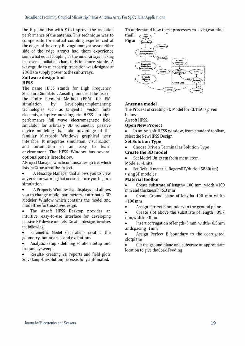
To understand how these processes co- exist, examine the illustration shown fig Figure (9): Process flow in hfss.
The name HFSS stands for High Frequency Structure Simulator. Ansoft pioneered the use of the Finite Element Method (FEM) for EM simulation by Developing/implementing technologies such as tangential vector finite elements, adaptive meshing, etc. HFSS is a high performance full wave electromagnetic field simulator for arbitrary 3D volumetric passive device modeling that take advantage of the familiar Microsoft Windows graphical user interface. It integrates simulation, visualization and automation in an easy to learn environment. The HFSS Window has several optional panels, listed below. A Project Manager which contains a design tree which lists the Structure of the Project. A Message Manager that allows you to view any error or warning that occurs before you begin a simulation. A Property Window that displays and allows you to change model parameters or attributes. 3D Modeler Window which contains the model and model tree for the active design. The Ansoft HFSS Desktop provides an intuitive, easy-to-use interface for developing passive RF device models. Creating designs, involves the following: Parametric Model Generation- creating the geometry, boundaries and excitations Analysis Setup - defining solution setup and frequency sweeps Results- creating 2D reports and field plots Solve Loop - the solution process is fully automated.
Antenna model The Process of creating 3D Model for CLTSA is given below. An soft HFSS. Open New Project In an An soft HFSS window, from standard toolbar, select the New HFSS Design. Set Solution Type Choose Driven Terminal as Solution Type Create the 3D model Set Model Units cm from menu item Modeler>Units Set Default material Rogers RT/duriod 5880(tm) using 3D modeler Material toolbar Create substrate of length= 100 mm, width =100 mm and thickness h=5.3 mm Create Ground plane of length= 100 mm width =100 mm Assign Perfect E boundary to the ground plane Create slot above the substrate of length= 39.7 mm, width =30 mm Insert corrugation of length=3 mm, width= 0.5mm and spacing=1 mm Assign Perfect E boundary to the corrugated slot plane Cut the ground plane and substrate at appropriate location to give the Coax Feeding

20
Create Coax and inner conducting Pin Boundary Conditions. The following boundary conditions must be applied to this device: Perfect E boundary on the top of the dielectric (simulates a metal layer Perfect E boundary on the bottom of the dielectric (simulates a metal layer) Perfect E boundary on the trace (simulates a metal layer) Radiation boundary on the long sides of the dielectric Now, select the top face, bottom face and the strip using the control key. With these three items selected, right click in the \white {space" of the 3D modeler window and highlight \Assign Boundary," and click \Perfect E...” Click OK. 3D Modeler window This is the area where you create the model geometry. This window consists of the model view area (or grid) and the history tree. The history tree documents the actions that have been taken in the model Project Manager with Project Tree The project manager window displays view area, and provides alternative way to select objects in the model view area details about all open HFSS projects. Each project ultimately includes a geometric model, its boundary conditions and material assignments, solution and post processing information. Properties Window The properties window consists of two tabs. The command tab displays information about an action selected in the history tree that was performed to either create an object or modify an object. The attribute tab displays information about the material and display properties of a selected object. This window is used when a simulation is running to monitor the solution’s progress. Message Manager This window displays messages associated with a pro0ject's development (such as error messages about the design's setup).
Setting up HFSS Before you can use HFSS for the time, there are a couple of items that need to be configured for efficient and accurate operation. 1. On the Tools menu, select Options => General Options ..., click the Default 2. Units tab and ensure that Length is set to mm. Click OK. 3. On the Tools menu, select Options => HFSS Options..., ensure they Include ferrite materials check box is checked. Click the Solver tab, set the number of Processors to 4, Desired RAM Limit (MB) to 6000 and the Maximum RAM Limit (MB) to 8000.Click OK. Figure (10): 3D model of modified ltsa
Analysis Setup Figure (11): Procedure of antenna.
Creating the Center Trace We will create the cent0er trace as an in thin strip. To do this, we select Draw=> helix in the menu. We can the size and location of the helix in the manner as for the dielectric above. Our strip width is 8.66mm, and 1000mm long, so the position is (-100,-8.66/2,0) and X Size = 200mm, Y Size = 8.66mm. Since the trace has no thickness, we do not apply any material
21
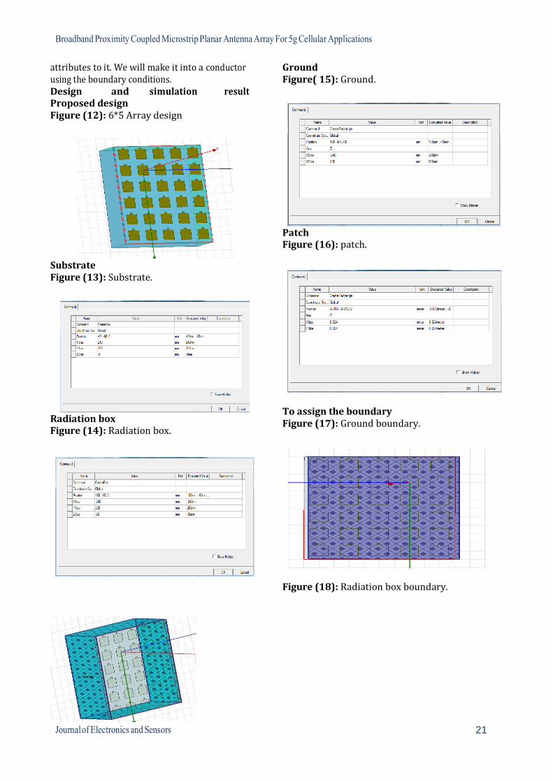
attributes to it. We will make it into a conductor using the boundary conditions. Design and simulation result Proposed design Figure (12): 6*5 Array design
Substrate Figure (13): Substrate.
Radiation box Figure (14): Radiation box.
Ground Figure( 15): Ground.
Patch Figure (16): patch.
To assign the boundary Figure (17): Ground boundary.
Figure (18): Radiation box boundary.

22
To assign the excitation Figure (19): Excitation boundary.
Simulation result Gain
Solution setup Figure( 20): solution setup.
Validation check Figure (21): Final arrary antenna.
Gain is an antenna property dealing with an antenna’s ability to direct its radiated power in a desired direction, or synonymously, to receive energy preferentially from a desired direction. The gain of the proposed antenna is 8dB. Figure (22): Final output of mircostrip antenna.
Fabrication Of Microstrip Patch Antenna This chapter deals with fabrication process. Fabricationof microstrio patch antenna • Any drawing software example paint. Draw structure of patch of microstrip antenna. • The black foot print of the antenna is printed on the transparent film and the dimensions are controlled. • We will use two chemicals one for developing one for etching the copper. • Both chemicals are inserted in the approximate bath. The etcher should be heated approximately for 20mins. • Meanwhile the film is rectangular cut (slightly larger than the size of the ground plane). • The marks are drawn on the double sided copper-clad material. We carefully attach the film on top • The black part of the film will act as a shielding mask, during the photo- exposure process. • The area that is masked will maintain its photoresist properties and eventually will protect copper from etching.

23
• UV light exposure (the proper surface should face the light approximately equal to 2 mins). • We remove the sticker from ground plane. The chemical process begins by inserting the board in the developer. • The board remains in the developer tank for 1minutes. • Developing process • Etching • The board is washed inside the water . The board is inserted into the etcher where copper will be etched by all UV exposed areas. • It should remain in etcher for 9min. Copper has been etched according to the design. • Antenna is washed under water. Photoresist is removed from the copper. Fabrication output Figure (23): fabrication output
Application for microstrip patch antenna Figure (24): using Gps.
Applications of 5g cellular This chapter deals with a application of the 5g cellular. Applications High-speed mobile network: 5G will revolutionize the mobile experience with supercharged wireless network, which can support up to 10 to 20 GBPS of data download speed. It is equivalent to a fiber optic Internet connection accessed wirelessly. Compared to conventional mobile transmission technologies, voice and high- speed data can be simultaneously transferred efficiently in 5G.Low latency is one of the most important features of 5G technology which is significant for autonomous driving and mission critical applications. 5G networks are capable of latency less than a millisecond. Entertainment and multimedia: Analysts found that 55 percentage of mobile Internet traffic has been used for video downloads globally in 2015. This trend will increase in future and high definition video streaming will be common in future.5G will offer a high definition virtual world on your mobile phone. High speed streaming of 4K videos only takes few seconds and it can support crystal clear audio clarity. InternetofThings–Connecting everything: Internet of Things (IoT) is another broad area for development using supercharged 5G wireless network. Internet of Things will connect every objects, appliances, sensors, devices and applications

24
into Internet. IoT applications will collects huge amount of data from millions of devices and sensors. It requires an efficient network for data collection, processing, transmission, control and real-time analytics. Smart Home: Smart home appliances and products are catching up the market today. Smart home concept will utilize 5G networks for device connectivity and monitoring of applications.5G wireless network will be utilized by smart appliances which can be configured and accessed from remote locations, closed circuit cameras will provide high quality real-time video for security purposes. Logistics and shipping: Logistic and shipping industry can make use of smart 5G technology for goods tracking, fleet management, centralized database management, staff scheduling and real-time delivery tracking and reporting. Smart cities: Smart city application like traffic management, Instant weather update, local area broadcasting, energy management, smart power grid, smart lighting of street, water resource management, crowd management, emergency response etc.… can use reliable 5G wireless network for its functioning. Industrial IOT: Future industries will depend on smart wireless technologies like 5G and LTE advanced for efficient automation of equipment, predictive maintenance, safety, process tracking, smart packing, shipping, logistics and energy management. Smart sensor technology offers unlimited solutions for industrial IoT for smarter, safe, cost effective and energy efficient industrial operation. Smart farming: 5G technology will be used for agriculture and smart farming in future. Using smart RFID sensors and GPS technology, farmers can track location of livestock and manage them easily.Smart sensors can be used for irrigation control, access control and energy management. Fleet management: Many companies are using smart tracking devices for fleet management, 5G technology will provide much better solutions for location tracking and fleet management.
Health care and mission critical applications: 5G technology will support medical practitioners to perform advanced medical le procedures with reliable wireless network connected to another side of the globe. Connected classrooms will help students to attend seminars and important lecturers. People with chronic medical conditions will benefit from smart devices and real-time monitoring. Doctors can connect with patients from anywhere anytime and advice them when necessary. Scientists are working on smart medical devices which can perform remote surgery. Advantages of HFSS This chapter deals with a advantages of hfss. Advantages
HFSS is an interactive simulation system whose basic mesh element is a tetrahedron. This allows you to solve any arbitrary 3D geometry, especially those with complex curves and shapes, in a fraction of the time it would take using other techniques.
An soft pioneered the use of the Finite Element Method (FEM) for EM simulation by developing / implementing technologies such as tangential vector finite elements, adaptive meshing. .
HFSS has evolved over a period of years with input from many users and industries. In industry, Ansoft HFSS is the tool of choice for High productivity research, development, and virtual prototyping Conclusion and Future scope Conclusion The design of a novel proximity coupled microstrip planar antenna is proposed. The structure is based on a series feeding technique that allows for a tight planar array configuration to be easily constructed. This is very useful in applications where compact size is a major requirement. It may further be enhanced for phased array applications. The stability of the structure is illustrated by the similarities in the simulated results making it very suitable for integration in 5G Applications.

25
Future scope In addition, this report also contains an evaluation of the following antennas on a common platform: shorted patch, CPW-feed square slot and asymmetric E-shaped antenna. In particular, we evaluate the effect of a 2U CubeSat body on their performance. Our results show that the performance of the CPW-feed square slot antenna is affected significantly by the 2U CubeSat body if due care is not taken. We propose to use a PVC plastic sheet between the antenna and the CubeSat body to overcome this problem and to improve performance. Finally, we and that the asymmetric E-shaped patch antenna design to be the most suitable design for pico-satellite communications. It achieved a high gain of 7.3 dB, wide bandwidth of 2300 MHz and has a small size; i.e., 34 × 13 mm2. References 1. Haraz O. M, Ali M M M, S. Alshebeili et al. (2015 ) Design of a 28/38 GHz Dual-Band Printed Slot Antenna for the Future 5G Mobile Communication Networks. IEEE International Symposium on Antennas and Propagation & USNC/URSI National Radio Science Meeting, Vancouver, BC; 19-24 2. Ojaroudiparchin N, Shen M,( 2015) Multi- Layer 5G Mobile Phone Antenna for Multi-User MIMO Communications,in Telecommunications Forum Telfor (TELFOR), Belgrade, Nov. 2015 . 3. Kothapudi V. K, Kumar.V,( March 2018 ) A 6-Port Two-Dimensional 3×3 Series- Fed Planar Array Antenna for Dual- Polarized X-Band Airborne Synthetic Aperture Radar Applications, IEEE Access, vol. 6, pp. 12001 - 12007. 4. H. Tsutsumi, Y. Kuwahara and H. Kamo, "Design of the series fed microstrip patch planar array antenna by the parato genetic algorithm," in Antennas and Propagation & USNC/URSI National Radio Science Meeting, 2015 IEEE International Symposium on, Vancouver, BC, Canada , July 2015. 5. J. Xu, W. Hong, H. Zhang and Y. Yu, "Design and measurement of array antennas for 77GHz automotive radar application," in Millimetre Waves and
Terahertz Technologies (UCMMT), 2017 10th UK-Europe-China Workshop on, Liverpool, UK, Sept. 2017. 6. L. Mall and R. Waterhouse, "Millimeter- wave proximity-coupled microstrip antenna on an extended hemispherical dielectric lens," IEEE Transactions on Antennas and Propagation , vol. 49, no. 12, pp. 1769 - 1772, 2001. 7. Y. Li and K.-M. Luk, "60-GHz Substrate Integrated Waveguide Fed Cavity-Backed Aperture-Coupled Microstrip Patch Antenna Arrays," IEEE Transactions on Antennas and Propagation, vol. 63, no. 3, pp. 1075 - 1085, 2015 . 8. D. Sun, W. Dou and L. You, "Application of Novel Cavity-Backed Proximity-Coupled Microstrip Patch Antenna to Design Broadband Conformal Phased Array," IEEE Antennas and Wireless Propagation Letters, vol. 9, pp. 1010 - 1013, 2010. 9. P. A. Dzagbletey and Y.-B. Jung, "Stacked Microstrip Linear Array for Millimeter- Wave 5G Baseband Communication," IEEE Antennas and Wireless Propagation Letters, vol. 17, no. 5, pp. 780 - 783, 2018. 10. S. Krishna, G. Mishra and S. K. Sharma, "A series fed planar microstrip patch array antenna with 1D beam steering for 5G spectrum massive MIMO applications," in Radio and Wireless Symposium (RWS), 2018 IEEE, Anaheim, CA, USA , Jan. 2018. 11. M. K. Ishfaq, T. A. Rahman, Y. Yamada and K. Sakakibara, "8×8 Phased series fed patch antenna array at 28 GHz for 5G mobile base station antennas," in Antennas and Propagation in Wireless Communications (APWC), 2017 IEEE-APS Topical Conference on, Verona, Italy , Sept. 2017 . 12. H. A. Diawuo and Y. B. Jung, "Wideband proximity coupled microstrip linear array design for 5G mobile communication," Microwave and Optical Technology Letters, vol. 59, no. 12, pp. 2996-3002, 2017. 13. A. Safaai-Jazi, "A New Formulation for the Design of Chebyshev Arrays," Antennas and Propagation, IEEE Transactions on, vol. 42, no. 3, pp. 439-443, August 2002. 14. Y. Hayashi, K. Sakakibara, M. Nanjo and S. Sugawa, "Millimeter-Wave Microstrip Comb-Line Antenna," Antennas and

26
Propagation, IEEE Transactions on, vol. 59, no. 2, pp. 398 - 406 , December 2010 . 15. C. Balanis, Antenna Theory: Analysis and Design, New York: Wiley, 1992. 16. D. M. Pozar and B. Kaufman, "Comparison of three methods for the measurement of printed antenna efficiency,," IEEE Trans. Antennas Propagat., vol. 36, no. 1, pp. 136-139, 1998. 17. Christos .Beretas (2018), Security and Privacy in Data Networks. J Electron Sensors; 1(1):1-20. 18. 18. Dutra RF (2018), Silva ACM, Saade J, et al. Acarbonink screen-printed immunoelectrode for Dengue virus NS1protein detection based on photosynthesized amine gold nanoparticles. J Electron Sensors;1 (1):1- 16. 19. Jahromi KK (2018), Aktaruzzaman Md, Jalili M Impact of overlapping in the radio coverage areas of multiple Wi-Fi access points on detecting encounters. J Electron Sensors;1 (1):1-18.
20. Aktaş A, Kırçiçek Y (2019), Investigation of Hybrid Renewable Energy Source and Hybrid Energy Storag e System. J Electron Sensors; 1 (1): 01-19. 21. Beretas C (2019), Internet of Things (IoT) is Smart Homes and the Risks. J Electron Sensors; 2(1): 1-4. 22. Moursy IA, ElDerini MN, Ahmed MA, (2019) Fault Tolerant Reliable Protocol (FTRP) Performance Evaluation in Wireless Sensor Networks: An Extensitive Study. J Electron Sensors; 2(1): 01-36. 23. Huang X et al., (2020), Electrochemical Determination of Trace Pb (II) by The Modified Glassy Carbon Electrode Multi- Walled Carbon Nanotubes-Nafion-Bi Film. J Electron Sensors; 3(1): 1- 12. 24. Lee H, Yang D, Kim SJ, et al., (2019), Verification of Antenna Sensor with Commercial Handsets By Applying Radiative Calibration Method. J Electron Sensors; 2(1): 01-06. 25. Shribala N, Mary JS, Mounika N, Manasa P et al., (2020), Polymer Electronic System. J Electron Sensors; 3(1): 01-15.
Citation: Shribala N (2020), Broadband Proximity Coupled Microstrip Planar Antenna Array For 5g Cellular Applications J Electron Sensors; 3(1): 1- 26. DOI: 10.31829/2689-6958/jes2020-3(1)-110 Copyright: © 2020 Shribala N. This is an open-access article distributed under the terms of the Creative Commons Attribution License, which permits unrestricted use, distribution, and reproduction in any medium, provided the original author and source are credited.