Embed Size (px)
Citation preview

Secondary electron emission yield from high aspect ratio carbon velvet surfacesChenggang Jin, Angelica Ottaviano, and Yevgeny Raitses
Citation: Journal of Applied Physics 122, 173301 (2017);View online: https://doi.org/10.1063/1.4993979View Table of Contents: http://aip.scitation.org/toc/jap/122/17Published by the American Institute of Physics
Articles you may be interested in
Energy distributions of electrons emitted by a biased laser-produced plasma at 1013 W cm-2Journal of Applied Physics 122, 173302 (2017); 10.1063/1.4997708
Ultraviolet out-of-band radiation studies in laser tin plasma sourcesJournal of Applied Physics 122, 173303 (2017); 10.1063/1.4986782
Standoff high energy laser induced oxidation spectroscopy (HELIOS)Journal of Applied Physics 122, 173102 (2017); 10.1063/1.4999918
Mechanism behind dry etching of Si assisted by pulsed visible laserJournal of Applied Physics 122, 173304 (2017); 10.1063/1.4991886
In-situ study of athermal reversible photocrystallization in a chalcogenide glassJournal of Applied Physics 122, 173101 (2017); 10.1063/1.5003575
Secondary electron emission characteristics of nanostructured silver surfacesJournal of Applied Physics 122, 153302 (2017); 10.1063/1.4989965
Secondary electron emission yield from high aspect ratio carbon velvetsurfaces
Chenggang Jin,a) Angelica Ottaviano, and Yevgeny Raitsesb)
Princeton Plasma Physics Laboratory, Princeton, New Jersey 08543, USA
(Received 3 July 2017; accepted 12 October 2017; published online 1 November 2017)
The plasma electrons bombarding a plasma-facing wall surface can induce secondary electron emis-
sion (SEE) from the wall. A strong SEE can enhance the power losses by reducing the wall sheath
potential and thereby increasing the electron flux from the plasma to the wall. The use of the materi-
als with surface roughness and the engineered materials with surface architecture is known to reduce
the effective SEE by trapping the secondary electrons. In this work, we demonstrate a 65% reduction
of SEE yield using a velvet material consisting of high aspect ratio carbon fibers. The measurements
of SEE yield for different velvet samples using the electron beam in vacuum demonstrate the depen-
dence of the SEE yield on the fiber length and the packing density, which is strongly affected by the
alignment of long velvet fibers with respect to the electron beam impinging on the velvet sample.
The results of SEE measurements support the previous observations of the reduced SEE measured
in Hall thrusters. Published by AIP Publishing. https://doi.org/10.1063/1.4993979
I. INTRODUCTION
The plasma-wall interaction in the presence of a strong
secondary electron emission (SEE) is relevant to various
plasma applications, including but not limited to electric pro-
pulsion,1,2 magnetic fusion devices,3,4 and plasma processing
devices.5,6 The plasma electrons bombarding the plasma-
facing wall surface can be scattered back to the plasma (back-
scattering SEE) or induce the ejection of the secondary elec-
trons from the material (true SEE). Independent on the nature
of secondary electrons, a strong SEE can enhance power losses
from the plasma due to the reduction of the plasma-wall sheath
potential.7 These losses increase with the increase of the total
SEE yield, which is defined as the ratio of the total emitted
electron flux, including true and backscattered electrons, to the
incident electron flux. When the SEE yield approaches 1, the
sheath may enter the so-called space-charge limited regime8 or
the inverse sheath regime.9 Under such conditions, the wall
acts as a very effective heat sink for the plasma. The suppres-
sion of SEE would be beneficial for many plasma applica-
tions1–6 in which the wall losses can cause a degradation of
performance of plasma devices or overheating of the plasma-
facing walls.
There are different ways to reduce and even suppress
the SEE yield. In Ref. 10, a surface treatment by different
processes, including electropolishing, carbon coating, and
vacuum pyrolyzing was shown to reduce the SEE yield by
28% compared to the untreated surfaces of the same materi-
als. Another approach to the suppression of SEE uses com-
plex structured surfaces, which trap the SEE electrons. For
example, coating of the aluminum surface with nanostruc-
tured graphene platelets allowed a 60% reduction of the total
SEE yield as compared to the uncoated aluminum surface.11
In Ref. 12, copper oxide nanowires grown on copper were
used to mitigate the effect of SEE in radio frequency (RF)
amplifiers. Moreover, Cu foams were shown to allow a dras-
tic (50%) reduction of the SEE yield.13 These foams were
proposed for application in particle accelerators. In Ref. 14,
it was demonstrated that the SEE yield from the tungsten
fuzz produced in a helium gas discharge, decreases signifi-
cantly compared to the smooth tungsten surface. Finally, the
experimental and theoretical studies of Ref. 15 investigated
the SEE yield from a micro-porous metal array, and demon-
strated a strong dependence of the SEE yield on the micro-
pore geometry and a number of micro-pores per unit area of
the array. They predicted and demonstrated a 45% reduction
of the SEE yield as compared to the Ag surface for an opti-
mized array.
Unlike a majority of the previous studies of SEE yield
from the architecture surfaces with low aspect ratio surface
non-uniformities (e.g., roughened surface) (AR � h/r< 102,
where AR is the aspect ratio of a surface non-uniformity, h
and r are the characteristic length and diameter of this non-
uniformity, respectively), this work is aimed to characterize
the SEE yield from high aspect ratio (AR> 103) velvet surfa-
ces. A carbon velvet material was already successfully used
for the suppression of SEE in Hall thrusters.16 A typical vel-
vet material consists of fully or partially aligned fibers
attached to a substrate. In Ref. 17, the SEE yield from the vel-
vet surface was investigated numerically and analytically.
The obtained analytical solution and simulations confirmed
the hypothesis of Ref. 15 that the total SEE yield of the velvet
can be significantly smaller than the SEE yield for a planar
surface and even for a roughened surface with a micro-
porous array. The reduction of SEE yield comes from the fact
that SEE electrons produced deep inside the velvet have a
large probability of hitting a fiber and getting absorbed by the
surface before exiting the velvet. Such trapped secondary
electrons do not contribute to the flux of secondary electrons
from the surface to the plasma. Thus, undesired effects of
a)Permanent address: College of Physics, Optoelectronics and Energy, and
Collaborative Innovation Center of Suzhou Nano Science and Technology,
Soochow University, Suzhou 215006, China.b)Author to whom correspondence should be addressed: [email protected]
0021-8979/2017/122(17)/173301/5/$30.00 Published by AIP Publishing.122, 173301-1
JOURNAL OF APPLIED PHYSICS 122, 173301 (2017)

SEE on the plasma can be greatly suppressed. In this paper,
the total SEE yield from various carbon velvet surfaces was
directly measured in vacuum using an electron beam. In par-
ticular, it is shown that the SEE yield depends on the velvet
characteristics, including the fiber length and the fiber pack-
ing density, and the angle of incidence of the primary elec-
trons with respect to the velvet substrate.
II. VELVET SAMPLES AND EXPERIMENTAL SETUP
A. Determination of the actual packing densityof velvet samples
The total SEE yield was characterized for five different
carbon velvet samples with different packing densities and
fiber lengths (Table I), as well as planar graphite substrates
without velvet. The velvet samples are composed of cylindrical
carbon fibers of radius �3.5 lm attached to a planar graphite
surface of a 25 mm-diameter substrate. For an ideal velvet
sample with velvet fibers aligned normal to the substrate sur-
face, the designed (or manufacturer specified) packing density
is defined as the ratio of the total area of all the fiber tips
attached to the sample substrate to the total area of this sample.
For example, 3.0% of packing density indicates that 3.0% of
the sample is occupied by fiber tips when viewed from above.
However, a microscopic analysis of the velvet samples used in
these experiments revealed that for all these samples, there are
misaligned velvet fibers bended with respect to the planar sub-
strate surface of the samples. For example, Fig. 1 shows images
of a velvet sample obtained with an FEI Quanta 200 FEG
Environmental Scanning Electron Microscope (SEM). The
images were obtained by irradiation of the velvet sample with
the SEM electron beam of 15 keV at normal incidence to the
sample. It can be clearly seen that the fiber areas that are visible
in SEM micrographs include portions of the side surface of the
fibers as well as the fiber tips. This is because the primary elec-
trons of the SEM electron beam impinge these side walls pro-
ducing SEE electrons detected by a SEM detector.
It is reasonable to assume that in practical plasma appli-
cations of such velvet materials, the primary electrons directed
normal to the substrate surface would also hit the side walls of
the bended fibers. Therefore, from the standpoint of suppres-
sion of SEE by the trapping of secondary electrons, the actual
packing density is apparently different from the designed
packing density. Table I describes the geometrical characteris-
tics of the velvet samples including the fiber lengths, and the
designed and actual packing densities.
The actual packing density, A, was determined by post-
processing of several SEM micrographs for each carbon vel-
vet sample. The parameters of SEM, such as image contrast,
brightness, and beam spot size were kept constant for all the
velvet samples. The image processing consists of separating
all the pixels of the velvet images into fiber pixels and graph-
ite base pixels. This was achieved by thresholding the SEM
images at the average intensity of the graphite base pixels.
The actual packing density was then estimated as the ratio of
number of fiber pixels, nf, to the total number of pixels in an
image with horizontal and vertical pixel dimensions n and m,
respectively
A ¼ nf
n� m: (1)
Here, nf is defined as the number of pixels, which have an
intensity larger than the graphite base pixel intensity. Figure
1(b) shows the post-processed SEM micrograph using Eq. (1).
TABLE I. Properties of velvet samples used in the described experiments.
Sample
Fiber
length
(mm)
Designed packing
density (%)
Aspect ratio
(height/radius)
Actual packing
density (%)
Error
(%)
1 0.5 4 145 85 2.3
2 1.5 3.5 430 81 5.8
3 1.5 1.8 430 68 5
4 1.5 0.8 430 63 2.8
5 3 2.7 860 87 4.7
FIG. 1. (a) An SEM micrograph of carbon velvet with 1.5 mm fiber length
and the designed packing density (as specified by a manufacturer) 1.8%, (b)
the same SEM micrograph post-processed by thresholding the pixels of vel-
vet images. The actual packing density estimated using Eq. (1) is 69.5%.
173301-2 Jin, Ottaviano, and Raitses J. Appl. Phys. 122, 173301 (2017)

The error in the last column of Table I is the percent devi-
ation from the average actual packing density using 10 velvet
images for each sample. The uncertainty varies between the
samples due to non-uniformity in fiber orientation across the
surface of a single velvet sample. In the same sample, there is
a large spread in the angles of the velvet fibers, leading to
high error margins when averaging over all the real packing
densities of the sample. This feature is easily observed by sur-
veying the velvet surfaces using SEM.
B. Measurements of the total SEE yield
The measurements of the total SEE yield from the velvet
and graphite samples were conducted in an ultra-high vac-
uum chamber (base pressure at 1� 5� 10�8 Torr) using an
experimental setup similar to Ref. 18. A Kimball Physics
ELG-2 electron gun produced primary electrons with ener-
gies of 6–1000 eV. Throughout all the experiments described
in this paper, the maximum electron beam current did not
exceed 2 mA. For measurements, each sample was exposed
to the electron beam from the gun. In addition, in order to
shield the exposed sample from stray electric fields an alumi-
num collector was attached to the gun and placed above the
sample axisymmetrically with both the gun and the sample.
The collector was electrically insulated from the gun and the
sample in order to allow for changes of the collector bias
voltage with respect to the sample and the gun.
In experiments, the samples were exposed normal to the
beam and at 90� to the beam (Fig. 2). A Keithley 6485
picoammeter was used to measure the current in the sample
circuit and the collector circuit (Fig. 3). The electron beam
from the gun was first characterized using a Faraday cup with
an entrance opening of 3 mm-diameter to ensure that the
beam is centered on the sample. The primary electron current,
IPE, was measured on the sample biased toþ18 V with respect
to ground, while the collector was electrically connected to
the ground. A positive bias voltage of the sample ensured both
the collection of beam electrons by the sample circuit and the
suppression of secondary electrons from the sample. The sam-
ple current IS ¼ IPE � ISE, which includes contributions from
both secondary electrons, ISE, and the primary electrons, was
measured on the sample connected electrically to the ground
through the picoammeter. In these measurements, the collec-
tor was biased þ18 V with respect to grounded sample to pre-
vent the collection of tertiary electrons from the grounded
chamber wall. Then, the total SEE yield was deduced from
ce ¼ISE
IPE¼ IPE � IS
IPE¼ 1� IS
IPE: (2)
For each velvet sample, the total SEE yield was mea-
sured at normal and 45� incidence to the sample surface.
III. RESULTS AND DISCUSSIONS
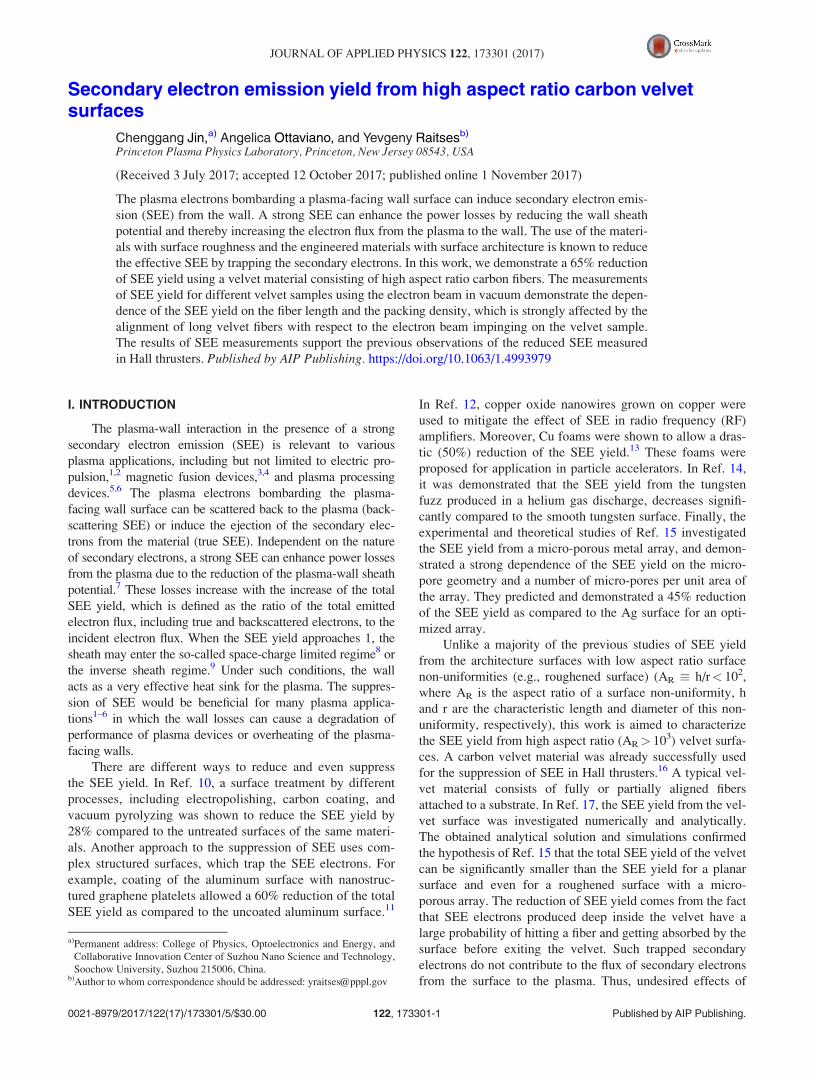
Figure 4 compares the total SEE yield from velvet sam-
ples 2, 3, and 4 with the same fiber length of 1.5 mm and the
total SEE yield from two planar graphite samples, including a
graphite sample from Ref. 19, and a graphite substrate used
for the velvet samples, but without velvet fibers. For all these
samples, the SEE yield reaches its maximum at �300 eV. For
the velvet samples, the SEE yield is lower than the SEE yield
from the planar graphite samples. This result supports the
hypothesis of the trapping of secondary electrons in velvet
fibers proposed in Ref. 16 and generally consistent with the
predictions of Ref. 17. For the samples with the same fiber
length, the sample with the largest packing density (sample 2)
FIG. 2. Schematics of the velvet sample with fibers (a) parallel to the pri-
mary electron beam, (b) perpendicular to the primary electron beam, and the
corresponding SEM micrographs of the velvet: (c) top view and (d) side
view.
FIG. 3. Experimental setup for measurements of the SEE yield: (a) measure-
ments of the primary electron current, and (b) measurements of the sample
current.
173301-3 Jin, Ottaviano, and Raitses J. Appl. Phys. 122, 173301 (2017)
has the lowest SEE yield (Fig. 4). The velvet samples display
a decreasing trend in the SEE yield with an increase of the
actual packing density from 63% to 81%. This trend does
not seem to hold for samples 3 and 4 with the actual packing
densities of 68% and 63%, respectively. The SEE yield of
sample 4 is somewhat smaller than the SEE yield of sample
3. This deviation from the trend is attributed to the errors
in the actual packing densities for sample 3 (5%) and sample
4 (2.8%). Reference 17 predicted the existence of optimal
packing density for a given fiber aspect ratio. This optimum
packing density was predicted due to a tradeoff between con-
tributions of the fiber tips and the side walls to the SEE from
the velvet. It is possible that in our set of velvet samples with
the same fiber aspect ratio, there are no samples with such
optimal packing density or the packing density larger than
this optimal value.
It is interesting that for the samples with the closest
packing densities (samples 1, 2 and 5 � 81%–87%), the sam-
ples with the shortest and longest fibers (samples 1 and 5)
have the larger yield than sample 2 with the fiber length of
1.5 mm. This result, which seemingly indicates the existence
of the optimal fiber length, is not consistent with the predic-
tions of Ref. 17 and is shown in Fig. 5. The model predicts
the reduction of the SEE yield with the fiber length probably
up to the saturation of the SEE yield above the certain fiber
length (aspect ratio) when the contribution of the SEE elec-
trons from the bottom of the velvet substrate becomes negli-
gible as compared to the contribution from the fiber tops and
sides. This unexpected result is likely due to the bending of
the longer fibers [Figs. 1(a) and 2(c)] of sample 5. Such
bended fibers are tilted away from the normal incidence of
the primary electron beam from the gun. Since the SEE yield
is affected by the incidence angle,20 the bended fibers have
larger SEE yield than the fibers aligned with the beam. The
bended fibers were not considered on the models and simula-
tions of Ref. 17 that may explain the earlier contradiction
between experiment and modeling.
To explore the effect of the incidence angle of primary
electrons on SEE, we conducted measurements of the total
SEE yield for both the normal incidence and the oblique inci-
dence. Figure 6 compares the total SEE yield from the velvet
sample 2 and the planar graphite substrate without velvet.
The SEE yield form substrate follows a 1=cosðhÞ dependence
(i.e., c0ð45�Þ ¼ c0ð0�Þ= cosð45�Þ, where c0 is the SEE yield
at the normal incidence). The increase of SEE yield at graz-
ing angles is due to the increased generation of the secondary
electrons within the material escape depth.21 Apparently, for
the velvet sample, the angular dependence does not follow
the cosine law. In particular, the yield at oblique incidence is
generally larger than it could be expected from cosine depen-
dence [Fig. 6, 1=cosðhÞ]. For example, near 50 eV, there is a
65% reduction in SEE yield for electrons incident at 0�,
FIG. 4. The total SEE yield from carbon velvet samples with a fiber length
of 1.5 mm and different values of the actual packing density (63%–81%) as
a function of the electron energy of primary electrons from the electron gun.
For comparison, the SEE yield for graphite substrate without velvet (red
filled circles) and Ref. 19 (black filled squares) are also plotted.
FIG. 5. The effect of the actual packing density on total SEE yield for the
velvet samples with different fiber lengths: 0.5 mm (pentagon-shape sym-
bols), 1.5 mm (circle-shape symbols), and 3 mm (triangle-shape symbols).
The measurements are shown for two energies of primary electrons: 50 eV
(black symbols) and 300 eV (red symbols).
FIG. 6. The effect of the incidence angle of primary electrons on the total
SEE yield measured for sample 2 (red symbols) (Table I) and for the graph-
ite substrate without velvet (black symbols). Measurements are shown for
normal incidence (pentagon-shape symbols) and the incidence angle of 45�
(triangle-shape symbols). Measurements at 45� are compared to values cal-
culated considering a 1/cos(h) dependence (dashed curve). SEE yield for the
graphite substrate at 0� (square-shape symbols), 45� (circle-shape symbols),
and calculated values (dashed curve) are also plotted for comparison.
173301-4 Jin, Ottaviano, and Raitses J. Appl. Phys. 122, 173301 (2017)
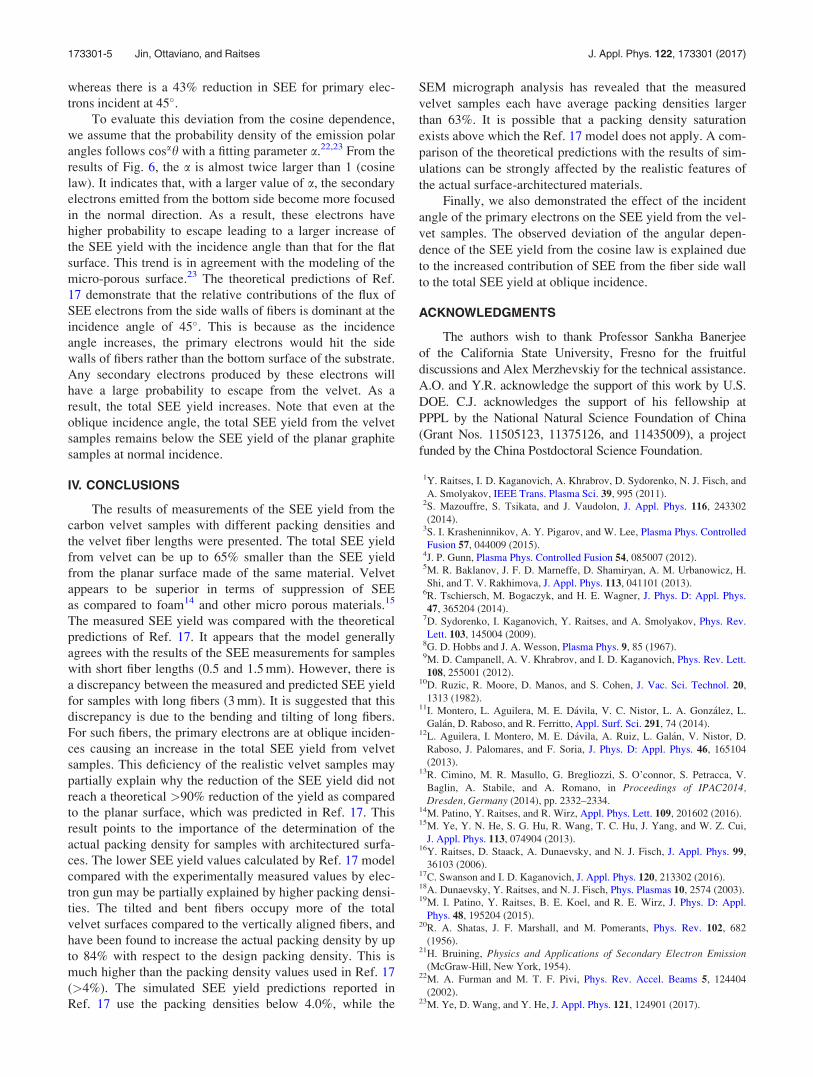
whereas there is a 43% reduction in SEE for primary elec-
trons incident at 45�.To evaluate this deviation from the cosine dependence,
we assume that the probability density of the emission polar
angles follows cosah with a fitting parameter a.22,23 From the
results of Fig. 6, the a is almost twice larger than 1 (cosine
law). It indicates that, with a larger value of a, the secondary
electrons emitted from the bottom side become more focused
in the normal direction. As a result, these electrons have
higher probability to escape leading to a larger increase of
the SEE yield with the incidence angle than that for the flat
surface. This trend is in agreement with the modeling of the
micro-porous surface.23 The theoretical predictions of Ref.
17 demonstrate that the relative contributions of the flux of
SEE electrons from the side walls of fibers is dominant at the
incidence angle of 45�. This is because as the incidence
angle increases, the primary electrons would hit the side
walls of fibers rather than the bottom surface of the substrate.
Any secondary electrons produced by these electrons will
have a large probability to escape from the velvet. As a
result, the total SEE yield increases. Note that even at the
oblique incidence angle, the total SEE yield from the velvet
samples remains below the SEE yield of the planar graphite
samples at normal incidence.
IV. CONCLUSIONS
The results of measurements of the SEE yield from the
carbon velvet samples with different packing densities and
the velvet fiber lengths were presented. The total SEE yield
from velvet can be up to 65% smaller than the SEE yield
from the planar surface made of the same material. Velvet
appears to be superior in terms of suppression of SEE
as compared to foam14 and other micro porous materials.15
The measured SEE yield was compared with the theoretical
predictions of Ref. 17. It appears that the model generally
agrees with the results of the SEE measurements for samples
with short fiber lengths (0.5 and 1.5 mm). However, there is
a discrepancy between the measured and predicted SEE yield
for samples with long fibers (3 mm). It is suggested that this
discrepancy is due to the bending and tilting of long fibers.
For such fibers, the primary electrons are at oblique inciden-
ces causing an increase in the total SEE yield from velvet
samples. This deficiency of the realistic velvet samples may
partially explain why the reduction of the SEE yield did not
reach a theoretical >90% reduction of the yield as compared
to the planar surface, which was predicted in Ref. 17. This
result points to the importance of the determination of the
actual packing density for samples with architectured surfa-
ces. The lower SEE yield values calculated by Ref. 17 model
compared with the experimentally measured values by elec-
tron gun may be partially explained by higher packing densi-
ties. The tilted and bent fibers occupy more of the total
velvet surfaces compared to the vertically aligned fibers, and
have been found to increase the actual packing density by up
to 84% with respect to the design packing density. This is
much higher than the packing density values used in Ref. 17
(>4%). The simulated SEE yield predictions reported in
Ref. 17 use the packing densities below 4.0%, while the
SEM micrograph analysis has revealed that the measured
velvet samples each have average packing densities larger
than 63%. It is possible that a packing density saturation
exists above which the Ref. 17 model does not apply. A com-
parison of the theoretical predictions with the results of sim-
ulations can be strongly affected by the realistic features of
the actual surface-architectured materials.
Finally, we also demonstrated the effect of the incident
angle of the primary electrons on the SEE yield from the vel-
vet samples. The observed deviation of the angular depen-
dence of the SEE yield from the cosine law is explained due
to the increased contribution of SEE from the fiber side wall
to the total SEE yield at oblique incidence.
ACKNOWLEDGMENTS
The authors wish to thank Professor Sankha Banerjee
of the California State University, Fresno for the fruitful
discussions and Alex Merzhevskiy for the technical assistance.
A.O. and Y.R. acknowledge the support of this work by U.S.
DOE. C.J. acknowledges the support of his fellowship at
PPPL by the National Natural Science Foundation of China
(Grant Nos. 11505123, 11375126, and 11435009), a project
funded by the China Postdoctoral Science Foundation.
1Y. Raitses, I. D. Kaganovich, A. Khrabrov, D. Sydorenko, N. J. Fisch, and
A. Smolyakov, IEEE Trans. Plasma Sci. 39, 995 (2011).2S. Mazouffre, S. Tsikata, and J. Vaudolon, J. Appl. Phys. 116, 243302
(2014).3S. I. Krasheninnikov, A. Y. Pigarov, and W. Lee, Plasma Phys. Controlled
Fusion 57, 044009 (2015).4J. P. Gunn, Plasma Phys. Controlled Fusion 54, 085007 (2012).5M. R. Baklanov, J. F. D. Marneffe, D. Shamiryan, A. M. Urbanowicz, H.
Shi, and T. V. Rakhimova, J. Appl. Phys. 113, 041101 (2013).6R. Tschiersch, M. Bogaczyk, and H. E. Wagner, J. Phys. D: Appl. Phys.
47, 365204 (2014).7D. Sydorenko, I. Kaganovich, Y. Raitses, and A. Smolyakov, Phys. Rev.
Lett. 103, 145004 (2009).8G. D. Hobbs and J. A. Wesson, Plasma Phys. 9, 85 (1967).9M. D. Campanell, A. V. Khrabrov, and I. D. Kaganovich, Phys. Rev. Lett.
108, 255001 (2012).10D. Ruzic, R. Moore, D. Manos, and S. Cohen, J. Vac. Sci. Technol. 20,
1313 (1982).11I. Montero, L. Aguilera, M. E. D�avila, V. C. Nistor, L. A. Gonz�alez, L.
Gal�an, D. Raboso, and R. Ferritto, Appl. Surf. Sci. 291, 74 (2014).12L. Aguilera, I. Montero, M. E. D�avila, A. Ruiz, L. Gal�an, V. Nistor, D.
Raboso, J. Palomares, and F. Soria, J. Phys. D: Appl. Phys. 46, 165104
(2013).13R. Cimino, M. R. Masullo, G. Bregliozzi, S. O’connor, S. Petracca, V.
Baglin, A. Stabile, and A. Romano, in Proceedings of IPAC2014,Dresden, Germany (2014), pp. 2332–2334.
14M. Patino, Y. Raitses, and R. Wirz, Appl. Phys. Lett. 109, 201602 (2016).15M. Ye, Y. N. He, S. G. Hu, R. Wang, T. C. Hu, J. Yang, and W. Z. Cui,
J. Appl. Phys. 113, 074904 (2013).16Y. Raitses, D. Staack, A. Dunaevsky, and N. J. Fisch, J. Appl. Phys. 99,
36103 (2006).17C. Swanson and I. D. Kaganovich, J. Appl. Phys. 120, 213302 (2016).18A. Dunaevsky, Y. Raitses, and N. J. Fisch, Phys. Plasmas 10, 2574 (2003).19M. I. Patino, Y. Raitses, B. E. Koel, and R. E. Wirz, J. Phys. D: Appl.
Phys. 48, 195204 (2015).20R. A. Shatas, J. F. Marshall, and M. Pomerants, Phys. Rev. 102, 682
(1956).21H. Bruining, Physics and Applications of Secondary Electron Emission
(McGraw-Hill, New York, 1954).22M. A. Furman and M. T. F. Pivi, Phys. Rev. Accel. Beams 5, 124404
(2002).23M. Ye, D. Wang, and Y. He, J. Appl. Phys. 121, 124901 (2017).
173301-5 Jin, Ottaviano, and Raitses J. Appl. Phys. 122, 173301 (2017)


![Investigation of electropolishing characteristics of tungsten in ......of electropolishing tungsten has been studied by Wang et al. [21], and they discovered that electropolishing](https://img.dokumen.tips/doc/110x75/60eb316d7c2235457f18455e/investigation-of-electropolishing-characteristics-of-tungsten-in-of-electropolishing.jpg)


![Plasma Electrolytic Oxidation as a modern method to … Electrolytic Oxidation as a modern method ... The modification in nanoscale is possible by using electropolishing [1-6], magnetoelectropolishing](https://img.dokumen.tips/doc/110x75/5afa6fff7f8b9ae92b8dc1d9/plasma-electrolytic-oxidation-as-a-modern-method-to-electrolytic-oxidation-as.jpg)