Embed Size (px)
Citation preview

8/7/2019 jntu ece comprahensiv viva
http://slidepdf.com/reader/full/jntu-ece-comprahensiv-viva 1/87
COMPHRAHENSIV VIVA
TRR ENGINEERING COLLEGE [email protected]
A Report about
COMPRAHENSIV VIVA
Submitted By
RAVI SANKAR
(Hall Ticket No.: 08D15A0408)
BACHELOR OF TECHNOLOGY
IN
ELECTRONICS AND COMMUNICATION ENGINEERING
DEPARTMENT OF ELECTRONICS AND COMMUNICATION ENGINEERING
TRR ENGINEERING COLLEGE
(An ISO 9000: 2000 Certified Institution)
AFFILIATED TO JAWAHARLAR NEHRU TECHNOLOGICAL UNIVERSITY
HYDERABAD
PATANCHERU
2007 - 2011

8/7/2019 jntu ece comprahensiv viva
http://slidepdf.com/reader/full/jntu-ece-comprahensiv-viva 2/87
COMPHRAHENSIV VIVA
TRR ENGINEERING COLLEGE [email protected]
CONTENTS
1. SECTION ± I
A. NETWORKS
B. CONTROL SYSTEM
C. COMPUTER ORGANIZATION
D. MICROPROCESSOR & INTERFACING
E. MICROCONTROLLER APPLICATION
2. SETION ± II
A. ELECTRONIC DEVICES & CIRCUITS
B. PULSE & DIGITAL CIRCUITS
C. LINEAR IC APPLICATIONS
D. DIGITAL IC APPLICATIONS
E. VLSI
3. SECTION ± III
A. PTSP
B. SIGNALS & SYSTEMS
C. DIGITAL SIGNAL PROCESSING
D. DIGITAL IMAGE PROCESSING

8/7/2019 jntu ece comprahensiv viva
http://slidepdf.com/reader/full/jntu-ece-comprahensiv-viva 3/87
COMPHRAHENSIV VIVA
TRR ENGINEERING COLLEGE [email protected]
4. SECTION ± IV
A. EMTL
B. AWP
C. MICROWAVE ENGINEERING
D. OPTICAL COMMUNICATION
5. SECTION ± V
A. ANALOG COMMUNICATION
B. DIGITAL COMMUNICATION
C. TSSN
D. CMC
E. RADAR SYSTEM

8/7/2019 jntu ece comprahensiv viva
http://slidepdf.com/reader/full/jntu-ece-comprahensiv-viva 4/87
COMPHRAHENSIV VIVA
TRR ENGINEERING COLLEGE [email protected]
SECTION -I

8/7/2019 jntu ece comprahensiv viva
http://slidepdf.com/reader/full/jntu-ece-comprahensiv-viva 5/87
COMPHRAHENSIV VIVA
TRR ENGINEERING COLLEGE [email protected]
N ETWORK AN ALYSIS

8/7/2019 jntu ece comprahensiv viva
http://slidepdf.com/reader/full/jntu-ece-comprahensiv-viva 6/87
COMPHRAHENSIV VIVA
TRR ENGINEERING COLLEGE [email protected]
1. What is Voltage and Current Sources?
Ans. Real voltage sources can be represented as ideal voltage sources in series with aresistance r, the ideal voltage source having zero resistance. Real current sources can be
represented as ideal current sources in parallel with a resistance r, the ideal current source
having infinite resistance.
2. Define Mutual- and Self-Induction ?
Ans. The changing magnetic field created by one circuit (the primary) can induce a changing
voltage and/or current in a second circuit (the secondary).
The mutual inductance, M, of two circuits describes the size of the voltage in the secondary
induced by changes in the current of the primary:
change in I (primary)
V(secondary) = - M * ----------------------
change in time
The units of mutual inductance are henry, abbreviated "H".
A circuit can create changing magnetic flux through itself, which can induce an opposing
voltage in itself. The size of that opposing voltage is
change in I
V(opposing) = - L * -------------
change in time
where L is the self-inductance of the circuit, again measured in henries

8/7/2019 jntu ece comprahensiv viva
http://slidepdf.com/reader/full/jntu-ece-comprahensiv-viva 7/87
COMPHRAHENSIV VIVA
TRR ENGINEERING COLLEGE [email protected]
3. Define bandwidth quality factor (Q)?
Ans. The bandwidth of an accelerometer refers to it's useful range of operating frequencies. Thisis usually defined by the frequency where the amplitude ratio falls to 0.5, the 3 dB point.
A system's quality factor, Q, describes the sharpness of the system's response. Q is equal to theratio of the center frequency to the bandwidth. Q is also used to describe the amplitude of theresonant response, which is roughly equal to resonant frequency divided by the driving
frequency.
4. Brief explanation about Independent & Dependent Voltage & current Sources?
Ans. Independent Voltage Sources
An ideal independent voltage source is a two-terminal circuit element where the voltage across it
a) is independent of the current through itb) can be specified independently of any other variable in a circuit.
Independent current Sources
In contrast to ideal independent voltage sources, an ideal independent current source is a two-
terminal circuit element where the current passing through ita) is independent of the voltage across it
b) can be specified independently of any other variable in a circuit.
Dependent Voltage & current source
voltage or current source whose value is proportional to some other voltage or current in the
circuit. Thus, there are four different kinds of dependent sources; to describe an op-amp, weneeda voltage-dependent voltage source. However, the standard circuit-theoretical model for a
transistor contains a current-dependent current source. Dependent sources do not serve as inputsto a circuit like independent sources. They are used to model active circuits: those containing
electronic elements. The RLC circuits we have been considering so far are known as passivecircuits.
5. Maximum Power Transfer Theorem?
Ans. Any complex circuit or network can be replaced by a single energy source in series with asingle internal source resistance, R S. Generally, this source resistance or even impedance if
inductors or capacitors are involved is of a fixed value in Ohm´s. However, when we connect aload resistance, R L across the output terminals of the power source, the impedance of the load
will vary from an open-circuit state to a short-circuit state resulting in the power being absorbedby the load becoming dependent on the impedance of the actual power source. Then for the load
resistance to absorb the maximum power possible it has to be "Matched" to the impedance of thepower source and this forms the basis of Maximum Power Transfer.
8/7/2019 jntu ece comprahensiv viva
http://slidepdf.com/reader/full/jntu-ece-comprahensiv-viva 8/87
COMPHRAHENSIV VIVA
TRR ENGINEERING COLLEGE [email protected]
Maximum Power Transfer is another useful analysis method to ensure that the maximumamount of power will be dissipated in the load resistance when the value of the load resistance is
exactly equal to the resistance of the power source. The relationship between the load impedanceand the internal impedance of the energy source will give the power in the load.
6. What is H - Parameters for
two-port network?
Ans. A two-port network (a kind of four-terminal network or quadripole) is an electrical
network or device with two pairs of terminals connected together internally by an electrical
network. Two terminals constitute a port if they satisfy the essential requirement known as the
port condition: the same current must enter and leave a port.
A two-port network makes possible the isolation of either a complete circuit or part of it andreplacing it by its characteristic parameters. Once this is done, the isolated part of the circuit
becomes a "black - box " with a set of distinctive properties, enabling us to abstract away itsspecific physical buildup, thus simplifying analysis. Any linear circuit with four terminals can be
transformed into a two-port network provided that it does not contain an independent source andsatisfies the port conditions.
There are a number of alternative sets of parameters that can be used to describe a linear two-
port network, the usual sets are respectively called z, y, h, g , and ABCD parameters, eachdescribed individually below. These are all limited to linear networks since an underlying
assumption of their derivation is that any given circuit condition is a linear superposition of various short-circuit and open circuit conditions.
7. What is Laplace Transform?
Ans. By applying the Laplace transform, one can change an ordinary differential equation into analgebraic equation, as algebraic equation is generally easier to deal with. Another advantage of Laplace transform is in dealing the external force is either impulsive , (the force lasts a very shot
time period such as the bat hits a baseball) or the force is on and off for some regular or irregular period of time
The Laplace transform of a function f (t ), defined for all real numbers t � 0, is the function F (s),
defined by:
The parameter s is a complex numbers:
with real numbers and .

8/7/2019 jntu ece comprahensiv viva
http://slidepdf.com/reader/full/jntu-ece-comprahensiv-viva 9/87
COMPHRAHENSIV VIVA
TRR ENGINEERING COLLEGE [email protected]
8. What is M-derived filter?
Ans. M-derived filters or m-type filters are a type of electronic filter designed using the imagemethod. They were invented by Otto Zobel in the early 1920s. This filter type was originally
intended for use with telephone multiplexing and was an improvement on the existing constant k
type filter.
[2]
The main problem being addressed was the need to achieve a better match of thefilter into the terminating impedances. In general, all filters designed by the image method fail togive an exact match, but the m-type filter is a big improvement with suitable choice of the
parameter m. The m-type filter section has a further advantage in that there is a rapid transitionfrom the cut-off frequency of the pass band to a pole of attenuation just inside the stop band.
Despite these advantages, there is a drawback with m-type filters; at frequencies past the pole of attenuation, the response starts to rise again, and m-types have poor stop band rejection. For this
reason, filters designed using m-type sections are often designed as composite filters with amixture of k-type and m-type sections and different values of m at different points to get the
optimum performance from both types.

8/7/2019 jntu ece comprahensiv viva
http://slidepdf.com/reader/full/jntu-ece-comprahensiv-viva 10/87
COMPHRAHENSIV VIVA
TRR ENGINEERING COLLEGE [email protected]
CON TR OL SYSTEMS

8/7/2019 jntu ece comprahensiv viva
http://slidepdf.com/reader/full/jntu-ece-comprahensiv-viva 11/87
COMPHRAHENSIV VIVA
TRR ENGINEERING COLLEGE [email protected]
1. what is Open Loop and closed loop control systems?
Ans. In Open-Loop control, no feedback loop is employed and system variations which cause
the output to deviate from the desired value are not detected or corrected.
A C losed -Loop system utilizes feedback to measure the actual system operating parameter beingcontrolled such as temperature, pressure, flow, level, or speed. This feedback signal is sent back
to the controller where it is compared with the desired system setpoint. The controller developsan error signal that initiates corrective action and drives the final output device to the desired
value. In the DC Motor Drive illustrated above, the tachometer provides a feedback.
2. Transfer Function of DC Servo motor?
Ans. I have recreated the servo system in the first diagram on the main power servo page here:
In this block diagram, I have represented the DC motor and the potentiometer attached to its
shaft as the transfer function G(s), and the amplifier with gain A. We will determine what theallowable range of A is to keep the system stable. The input of G(s) is the armature voltage of the
motor, ea, and its output is the motor shaft angular position, m.
From the block diagram,
The closed loop transfer function of this system is

8/7/2019 jntu ece comprahensiv viva
http://slidepdf.com/reader/full/jntu-ece-comprahensiv-viva 12/87
COMPHRAHENSIV VIVA
TRR ENGINEERING COLLEGE [email protected]
3. Define Steady state response?
Ans. The terms t ransient response arise naturally in the context of sine wave analysis. When the
input sine wave is switched on, the filter takes a while to ``settle down'' to a perfect sinewave at
the same frequency. The filter response during this ``settling'' period is called the t ransient response of the filter .
4. Define stability of a system?
Ans. The stability of a system relates to its response to inputs or disturbances. A system which
remains in a constant state unless affected by an external action and which returns to a constantstate when the external action is removed can be considered to be stable.
A systems stability can be defined in terms of its response to external impulse inputs..
Definition
A system is stable if its impulse response approaches zero as time approaches infinityThe system stability can also be defined in terms of bounded (limited) inputs.
Definition A system is stable if every bounded input produces a bounded output.
5. What is Gain margin?Ans. The gain margin is the amount of gain increase required to make the loop gain unity at the
frequency where the phase angle is ±180°. In other words, the gain margin is 1/g if g is the gainat the ±180° phase frequency. Similarly, the phase margin is the difference between the phase of
the response and ±180° when the loop gain is 1.0. The frequency at which the magnitude is 1.0 iscalled the unit y-g ain f requency or crossover f requency. It is generally found that gain margins of
three or more combined with phase margins between 30 and 60 degrees result in reasonabletrade-offs between bandwidth and stability.
6. What is Nyquist Plots?Ans. There are a number of polar graph options for studying control systems including the
nyquist, inverse polar plot and the nichols plot. The nyquist open loop polar plot indicates thedegree of stability, and the adjustments required and provides stability information for systems
containing time delays. Polar plots are not used exclusively because,without powerfulcomputing facilities, they can be difficult to generate at a detailed level and they do not directly
yield frequency values.

8/7/2019 jntu ece comprahensiv viva
http://slidepdf.com/reader/full/jntu-ece-comprahensiv-viva 13/87
COMPHRAHENSIV VIVA
TRR ENGINEERING COLLEGE [email protected]
7. What is lead±lag compensator ?
Ans. A lead±lag compensator is a component in a control system that improves an undesirable
frequency response in a feedback and control system. It is a fundamental building block inclassical control theory.
Both lead compensators and lag compensators introduce a pole±zero pair into the open loop
transfer function. The transfer function can be written in the Laplace domain as
where X is the input to the compensator, Y is the output, s is the complex Laplace transformvariable, z is the zero frequency and p is the pole frequency.
8. What is state variables?
Ans. In Control Engineering and other areas of science and engineering, state variables are usedto represent the states of a general system. The state variables can be used to describe the statespace of the system. The equations relating the current state and output of a system to its current
input and past states are called the state equations. The state equations for a linear time invariantsystem are expressed with Coefficient matrices.

8/7/2019 jntu ece comprahensiv viva
http://slidepdf.com/reader/full/jntu-ece-comprahensiv-viva 14/87
COMPHRAHENSIV VIVA
TRR ENGINEERING COLLEGE [email protected]
COMPUTER
ORGAN IZATIO N

8/7/2019 jntu ece comprahensiv viva
http://slidepdf.com/reader/full/jntu-ece-comprahensiv-viva 15/87
COMPHRAHENSIV VIVA
TRR ENGINEERING COLLEGE [email protected]
1. What are Functional units?
Ans. In order to carry out the operations like accepting data or instructions by way of input, tostores data, to process data as required by the user, to gives results in the form of output, and to
controls all operations inside a computer, the computer allocates the task between its various
functional units. The computer system is divided into three separate units for its operation. Theyare 1) arithmetic logical unit, 2) control unit, and 3) central processing unit.
2. What is micro-operation?A. Complex digital systems which deals with lots of tasks like logic operation, arithmetic
operation contains many hardware whose are interconnected among them is called micro-operation.
3. What is Control memory?
Ans. Control memory is a random access memory (RAM) consisting of addressable storage
registers. It is primarily used in mini and mainframe computers. It is used as a temporary storagefor data. Access to control memory data requires less time than to m a in memory; this speeds up
CPU operation by reducing the number of memory references for data storage and retrieval.Access is performed as part of a control section sequence while the master clock oscillator
is running. The control memory addresses are divided into two groups: a task mode andan executive (interrupt) mode.
4. What is decimal arithmetic unit ?
Ans. A decimal arithmetic unit is a digital function that performs decimal micro-operations. It
can add or subtract decimal numbers, usually by forming the 9's or 10'scomplement of thesubtrahend. The unit accepts coded decimal numbers and generates results in the same adopted
binary code. A single-stage decimal arithmetic unit consists of nine binary input variables andfive binary output variables, since a minimum of four bits is required to represent each coded
decimal digit. Each stage must have four inputs for the augend digit, four inputs for the addenddigit, and an input-carry. The outputs include four terminals for the sum digit and one for the
output-carry. Of course, there is a wide variety of possible circuit configurations dependent onthe code used to represent the decimal digits.
5. What is Cache Memory?
Ans. A CPU cache is a cache used by the central processing unit of a computer to reduce the
average time to access memory. The cache is a smaller, faster memory which stores copies of the
data from the most frequently used main memory locations. As long as most memory accesses
are cached memory locations, the average latency of memory accesses will be closer to the cache
latency than to the latency of main memory.

8/7/2019 jntu ece comprahensiv viva
http://slidepdf.com/reader/full/jntu-ece-comprahensiv-viva 16/87
COMPHRAHENSIV VIVA
TRR ENGINEERING COLLEGE [email protected]
When the processor needs to read from or write to a location in main memory, it first checks
whether a copy of that data is in the cache. If so, the processor immediately reads from or writes
to the cache, which is much faster than reading from or writing to main memory.
6. What are Peripheral devises?
Ans. Peripheral devise are the computer devices that are connected to the computer externally
such as printer, scanner, keyboard, mouse, tape device, microphone and external modem. Theycan be internal such as CD-ROM or internal modem and external as the scanner, printer and Zip
drive. Peripheral devices can be classified according to their functions.
Input: Input devices are the type of the computer devices that are used to provide the controlsignals to the computer. Keyboard and the Mouse are the examples of the input devices.
Output: Output devices are the devices that are used to display the results. Printer, scanner,speaker and the monitor are the examples of the output devices.
Storage: A storage device is a device that is used to store the input.
7. What is Parallel processing? Ans. Parallel processing is the simultaneous processing of the same task on two or more microprocessors in order to obtain faster results. The computer resources can include a
single computer with multiple processors, or a number of computers connected by a network, or a combination of both. The processors access data through shared memory. Some
supercomputer parallel processing systems have hundreds of thousands of microprocessors.
8. What is Interconnection Structures?
Ans. A computer consists of a set of components (CPU, memory, I/O) that communicate with each other.
The collection of paths connecting the various modules is call the Interconnection Structures. The design of this structure will depend on the exchange that must be made between
Modules.
8/7/2019 jntu ece comprahensiv viva
http://slidepdf.com/reader/full/jntu-ece-comprahensiv-viva 17/87
COMPHRAHENSIV VIVA
TRR ENGINEERING COLLEGE [email protected]
MICROPROCESSORS
AND IN T ERFACING

8/7/2019 jntu ece comprahensiv viva
http://slidepdf.com/reader/full/jntu-ece-comprahensiv-viva 18/87
COMPHRAHENSIV VIVA
TRR ENGINEERING COLLEGE [email protected]
1. Explain how IRET instruction is executed?
A. The IERT instruction is used at the end of the interrupt service routine to return execution to
the interrupted program . The 8086 copies return address from stack into IP and CS registers and
the stored value of flags back to the flag register .The RET instruction does not copy the flags
from the stack back to the flag register.
2. What is Branch Instruction?
Ans. Branch instructions perform a test by evaluating a logical condit ion and depending on the
outcome of the condition modify the program counter to take the branch or continue to the nextinstruction.
Branch instructions are always relat ive to the current program counter. That is, the next
instruction is obtained by adding a signed offset to current program counter:
PC += (int)offsetBranches are inherently relocat able. That is, the program can be moved to any other block of
memory and still execute correctly. Jump instructions, by contrast, specify an absolute memoryreference. If the underlying program is moved in memory, those jump memory references
pointing to the interior of the moved block must be changed.
3. What is the Need for Direct-Memory Access (DMA)?
Ans. Computers often require rapid transfers of large amounts of data from one part of the
system to another part.
E.g., disk controllers, video controllers, network controllers, etc.
The Problem: to be transferred, using programmed or minute more than a Large files couldtake interrupt I/O.
The Solution: Allow the Peripheral I/O device communicate directly with memory, commonly
called a Direct-Memory Access. With DMA data transfer rates of 10-50 million bytes per secondcan be achieved.
4. What is 8255 PPI - Programmable Peripheral Interface?
Ans. PPI - Programmable Peripheral InterfaceThe 8255A programmable peripheral interface (PPI) implements a general-purpose
I/O interface to connect peripheral equipment to a microcomputer system bus. Thecore's functional configuration is programmed by the system software so that external
logic is not required to interface peripheral devices.Features
� Three 8-bit Peripheral Ports - Ports A, B, and C� Three programming modes for Peripheral Ports: Mode 0 (Basic Input/Output),

8/7/2019 jntu ece comprahensiv viva
http://slidepdf.com/reader/full/jntu-ece-comprahensiv-viva 19/87
COMPHRAHENSIV VIVA
TRR ENGINEERING COLLEGE [email protected]
Mode 1 (Strobed Input/Output), and Mode 2 (Bidirectional)� Total of 24 programmable I/O lines
� 8-bit bidirectional system data bus with standard microprocessor interfaceControls.
5. What is Interrupt & what is the purpose of interrupt?
Ans. The meaning of µinterrupts¶ is to break the sequence of operation.While the cpu is
executing a program,on µinterrupt¶ breaks the normal sequence of executionof instructions,
diverts its execution to some other program called Interrupt Service Routine (ISR).After
executing ISR , the control is transferred back again to the main program.
6. what are the types of data communication in 8251?
A. 1. Asynchronous transmission
2. Asynchronous reception
3. Synchronous transmission
4. Synchronous reception
7.What is RISC?
Ans. RISC: Reduced I nstruction S et C omput er
Small, highly optimized set of instructions,Every instruction is executed in a single clock after it is fetched and decoded,
Very fast execution,
Less power consumption,
T he Advantag es of RIS C:
RISC instructions, being simple, can be hard- wire,
Processor can work at a high clock frequency and thus yields higher speed,
On-chip MMU, Floating point arithmetic units,
Chip cost is low,
More devises can place on chip,
Compilers produce more efficient codes in RISC p &
Loading and decoding of instructions in a RISC processor is simple and fast.

8/7/2019 jntu ece comprahensiv viva
http://slidepdf.com/reader/full/jntu-ece-comprahensiv-viva 20/87
COMPHRAHENSIV VIVA
TRR ENGINEERING COLLEGE [email protected]
8. Register Set of 8051-SFR?
Ans. Register Set of 8051-SFR
TH0-TL0 and TH1-TL116 bit timer registers
P0-P3 ± port latches
SP, PSW, IP ± Interrupt Priority, IE ± enable
TCON ± timer/counter control reg to turn on/off the timers, interrupt control flags for ext. int
like INT1 and INT0
TMOD ± modes of operation of timer/counter
SCON ± serial port mode control reg
SBUF ± serial data buffer for transmit and receive
PCON ± Power control reg ± power down bit, idle bit

8/7/2019 jntu ece comprahensiv viva
http://slidepdf.com/reader/full/jntu-ece-comprahensiv-viva 21/87
COMPHRAHENSIV VIVA
TRR ENGINEERING COLLEGE [email protected]
MICRO CON T ROLL ERS
AND APPL ICAT IONS

8/7/2019 jntu ece comprahensiv viva
http://slidepdf.com/reader/full/jntu-ece-comprahensiv-viva 22/87
COMPHRAHENSIV VIVA
TRR ENGINEERING COLLEGE [email protected]
1. What are 8051 microcontroller¶s Internal and External memories?
Ans. The 8051 has three very general types of memory. To effectively program the 8051 it isnecessary to have a basic understanding of these memory types.
The memory types are illustrated in the following graphic. They are: On-Chip Memory, ExternalCode Memory, and External RAM.
On-Chip Memory refers to any memory (Code, RAM, or other) that physically exists on the
microcontroller itself. On-chip memory can be of several types, but we'll get into that shortly.
External Code Memory is code (or program) memory that resides off-chip. This is often in theform of an external EPROM.
External RAM is RAM memory that resides off-chip. This is often in the form of standard static
RAM or flash RAM.
2. Write the signal description for TXD?
A. The pin 11 (p3.1) of 8051 microcontroller can be used as TXD. This pin is used to transfer
output from microcontroller for serial data transmission.
Initially the serial data in µSBUF¶ register then the contents of this register are transmitted to
output device serially (bit by bit).
At the end of the transmission T1 (Timer Interrupt) flag will be set.
4. 8051 microcontroller interrupts?
Ans. 8051 provides 5 vectored interrupts. They are -
1. 2. TF0
3. 4. TF1

8/7/2019 jntu ece comprahensiv viva
http://slidepdf.com/reader/full/jntu-ece-comprahensiv-viva 23/87
COMPHRAHENSIV VIVA
TRR ENGINEERING COLLEGE [email protected]
5. RI/TI
Out of these, and are external interrupts whereas Timer and Serial port interrupts aregenerated internally. The external interrupts could be negative edge triggered or low level
triggered. All these interrupt, when activated, set the corresponding interrupt flags. Except for
serial interrupt, the interrupt flags are cleared when the processor branches to the InterruptService Routine (ISR). The external interrupt flags are cleared on branching to Interrupt ServiceRoutine (ISR), provided the interrupt is negative edge triggered. For low level triggered external
interrupt as well as for serial interrupt, the corresponding flags have to be cleared by software bythe programmer.
4. What is Free running counter in 8051?
Ans. The Counter Free-Running block counts up until reaching the maximum value, 2N bit s
± 1,where N bit s is the number of bits. Then the counter overflows to zero and begins counting up
again.
After overflow, the counter always initializes to zero. However, if you select the global doublesoverride, the Counter Free-Running block does not wrap back to zero.
5. How printer inter faces to 8051MCU?
Ans. Printer has 8 data lines, and we use two control signals, busy and strobe. Busy pin is madeinput and strobe as output. First strobe pin is kept high, data to be printed is obtained at particular
port then, low to high transition is given to the strobe. then we keep checking the busy pin, if printer is busy then wait, after it becomes free then send next data. for printer interfacing we
used DB25 connector .
6. What is Real-Time Operating Systems in Microcontrollers?
Ans. Real-time embedded systems serve various purposes, such as to control or process data. A
real-time operating system is a piece of software with a set of APIs that developers can use tobuild applications. RTOSs support the need of some embedded systems to meet deadlines.
However, using an RTOS doesn't guarantee that a system will always meet the deadlines,because these systems also depend on the overall system's design. Although RTOSs for
embedded systems are predominantly used in high-end microprocessors or microcontrollers with32-bit CPUs, there is a growing trend to provide these features in mid-range (16-bit and 8-bit)
processor systems
7. What is RTX51 Tiny Real-Time Kernel?
Ans. RTX51 Tiny is a small real-time kernel designed for single-chip applications where code size is the
most important factor. The RTX51 Tiny kernel requires only 900 bytes of code space and is well-suited
for applications that don't need RTOS features like messaging, semaphores, and memory pool
management.

8/7/2019 jntu ece comprahensiv viva
http://slidepdf.com/reader/full/jntu-ece-comprahensiv-viva 24/87
COMPHRAHENSIV VIVA
TRR ENGINEERING COLLEGE [email protected]
RTX51 Tiny was designed for single-chip applications where no XDATA is available. However,
RTX51 Tiny may be used with any 8051 target system.
8. What is ARM microcontroller?
Ans. The microcontroller is a general purpose 32-bit microprocessor, which offers highperformance and very low power consumption. The ARM architecture is based on RISC
principles, and the instruction set and related decode mechanism are much simpler than those of microprogrammed CISCs. This simplicity results in a high instruction throughput and impressive
real-time interrupt response from a small and cost-effective processor core.
A 5-stage pipeline is employed so that all parts of the processing and memory systems canoperate continuously. At any one point in time, several operations are typically in progress:
subsequent instruction fetch, next instruction decode, instruction execution, memory access, andwrite-back .

8/7/2019 jntu ece comprahensiv viva
http://slidepdf.com/reader/full/jntu-ece-comprahensiv-viva 25/87
COMPHRAHENSIV VIVA
TRR ENGINEERING COLLEGE [email protected]
SECTION - II

8/7/2019 jntu ece comprahensiv viva
http://slidepdf.com/reader/full/jntu-ece-comprahensiv-viva 26/87
COMPHRAHENSIV VIVA
TRR ENGINEERING COLLEGE [email protected]
EL ECT RON IC DEVICES &
CIRCUIT S

8/7/2019 jntu ece comprahensiv viva
http://slidepdf.com/reader/full/jntu-ece-comprahensiv-viva 27/87
COMPHRAHENSIV VIVA
TRR ENGINEERING COLLEGE [email protected]
1. What are Electric and Magnetic fields
Ans. Wherever there is electricity, there are also electric and magnetic fields, invisible lines of force created by the electric charges. Electric fields result from the strength of the charge whilemagnetic fields result from the motion of the charge, or the current. Electric fields are easily
shielded: they may be weakened, distorted or blocked by conducting objects such as earth, trees,and buildings, but magnetic fields are not as readily blocked. Electric charges with opposite signs
(positive and negative) at-tract each other, while charges with the same sign repel each other.The forces of attraction and repulsion create electric fields whose strength is related to ³voltage
(elec-trical pressure). These forces of attraction or repulsion are carried through space fromcharge to charge by the electric field. The electric field is measured in volts per meter (V/m) or
in kilovolts per meter (kV/m).
2. What is the Fermi level for extrinsic semiconductors?
Ans. An extrinsic semiconductor is an intrinsic semiconductor doped with either electron donors
or electron acceptors which will increase the electron or hole concentrations respectively.
For an intrinsic semiconductor, the Fermi Energy level sits roughly at midpoint of the band gap,if the effective mass of holes and electrons is the same. When the semiconductor is doped, the
Fermi level moves either towards the conduction band if the doping is an electron donor or towards the valence band if the doping is an electron acceptor. For non-degenerate doping, the
3. What is Voltage regulator?
Ans. A voltage regulator is an electrical regulator designed to automatically maintain a constantvoltage level. A voltage regulator may be a simple "feed-forward" design or may include
negative feedback control loops. It may use an electromechanical mechanism, or electroniccomponents. Depending on the design, it may be used to regulate one or more AC or DC
voltages.
Electronic voltage regulators are found in devices such as computer power supplies where theystabilize the DC voltages used by the processor and other elements. In automobile alternators and
central power station generator plants, voltage regulators control the output of the plant. In anelectric power distribution system, voltage regulators may be installed at a substation or along
distribution lines so that all customers receive steady voltage independent of how much power isdrawn from the line.

8/7/2019 jntu ece comprahensiv viva
http://slidepdf.com/reader/full/jntu-ece-comprahensiv-viva 28/87
COMPHRAHENSIV VIVA
TRR ENGINEERING COLLEGE [email protected]
4. How Transistor works as an amplifier in common-emitter configuration?
Ans. When a transistor is connected in a common-emitter configuration, the input signal is
injected between the base and emitter, which is a low resistance, low-current circuit. As the inputsignal swings positive, it also causes the base to swing positive with respect to the emitter. Thisaction decreases forward bias which reduces collector current (IC) and increases collector voltage
(making VC more negative). During the negative alternation of the input signal, the base is drivenmore negative with respect to the emitter. This increases forward bias and allows more current
carriers to be released from the emitter, which results in an increase in collector current and adecrease in collector voltage (making VC less negative or swing in a positive direction). The
collector current that flows through the high resistance reverse-biased junction also flowsthrough a high resistance load (not shown), resulting in a high level of amplification.
5. What is Thermal runaway in BJT?
Ans. Leakage current increases significantly in bipolar transistors (notably germanium-based
bipolar transistors) as they increase in temperature. Depending on the design of the circuit, thisincrease in leakage current can increase the current flowing through the transistor and with it the
power dissipation. This causes a further increase in C±E current. This is frequently seen in apush±pull stage of a class AB amplifier. If the transistors are biased to have minimal crossover
distortion at room temperature, and the biasing is not made temperature dependent, as thetemperature rises, both transistors will be increasingly turned on, causing current and power to
further increase, eventually destroying one or both devices.
To avoid thermal runaway the operating point of BJT should be Vce � 1/2Vcc
6. What is input impedance?
Ans. The input impedance of an electrical network is the equivalent impedance "seen" by a
power source connected to that network. If the source provides known voltage and current, suchimpedance can be calculated using Ohm's Law. The input impedance is the Thévenin's
equivalent circuit of the electrical network, modeled by an RL (resistor-inductor) or an RC(resistor-capacitor) combination, with equivalent values that would result in the same response as
that of the network. It is also called Z11 in terms of Z-Parameters.
7. What is amplifier gain?
Ans. Amplifier gain stands for any of Voltage amplifier, Current amplifier, Trans resistanceTrans admittance amplifier

8/7/2019 jntu ece comprahensiv viva
http://slidepdf.com/reader/full/jntu-ece-comprahensiv-viva 29/87
COMPHRAHENSIV VIVA
TRR ENGINEERING COLLEGE [email protected]
Ve feed back amplifier depends on |1 | 1 , 1
b bA ve f ve f F "
Feed back reduces noise distortion, gain variation due to parameters, increases BW.
1 AF is called de-sensitivity factor.
8
. What is Wein Bridge oscillator?
Ans. A Wien bridge oscillator is a type of electronic oscillator that generates sine waves. It can
generate a large range of frequencies. The circuit is based on an electrical network originally
developed by Max Wien in 1891. The bridge comprises four resistors and two capacitors. It can
also be viewed as a positive feedback system combined with a band pass filter. Wien did not
have a means of developing electronic gain so a workable oscillator could not be realized.
Classic Wien bridge oscillator
0
0
; ;1
f
f
i
X X AA A
A X X F
F! ! !

8/7/2019 jntu ece comprahensiv viva
http://slidepdf.com/reader/full/jntu-ece-comprahensiv-viva 30/87
COMPHRAHENSIV VIVA
TRR ENGINEERING COLLEGE [email protected]
PUL SE AND DIGIT AL
CIRCUIT S

8/7/2019 jntu ece comprahensiv viva
http://slidepdf.com/reader/full/jntu-ece-comprahensiv-viva 31/87
COMPHRAHENSIV VIVA
TRR ENGINEERING COLLEGE [email protected]
1. What is attenuator?
Ans. An attenuator is an electronic device that reduces the amplitude or power of a signal
without appreciably distorting its waveform.
An attenuator is effectively the opposite of an amplifier, though the two work by differentmethods. While an amplifier provides gain, an attenuator provides loss, or gain less than 1.
Attenuators are usually passive devices made from simple voltage divider networks. Switchingbetween different resistances forms adjustable stepped attenuators and continuously adjustable
ones using potentiometers. For higher frequencies precisely matched low VSWR resistancenetworks are used.
2. What is transistor clipper?
Ans. A clipper is a device designed to prevent the output of a circuit from exceeding a
predetermined voltage level without distorting the remaining part of the applied waveform.
A clipping circuit consists of linear elements like resistors and non-linear elements like junction
diodes or transistors, but it does not contain energy-storage elements like capacitors. Clippingcircuits are used to select for purposes of transmission, that part of a signal wave form which lies
above or below a certain reference voltage level.
Thus a clipper circuit can remove certain portions of an arbitrary waveform near the positive or negative peaks. Clipping may be achieved either at one level or two levels. Usually under the
section of clipping, there is a change brought about in the wave shape of the signal.
3. How diode acts as a switch?
Ans. A diode consists of p-type and n-type semiconductor materials joined together. One may
approximate an "ideal" diode to a switch and simplify analysis of simple circuits
y Electrons in n-type semiconductorsy ³Holes in p-type semiconductors
When two different types of semiconductor materials are joined intimately, the movement of
holes and electrons combine near the junction, resulting in a depletion layer at the juncture.
A small barrier potential due to charged ions left behind is then created.
The circuit symbol used for a diode is a large black arrow, indicating conventional current flow
in the direction from p-type to n-type materials. A bar represents the junction, If a battery isapplied to the ends of the diode, the barrier potential provides resistance to any current flow

8/7/2019 jntu ece comprahensiv viva
http://slidepdf.com/reader/full/jntu-ece-comprahensiv-viva 32/87
COMPHRAHENSIV VIVA
TRR ENGINEERING COLLEGE [email protected]
4. What is a multi vibrator circuit?
Ans. A multivibrator is an electronic circuit used to implement a variety of simple two-statesystems such as oscillators, timers and flip-flops. It is characterized by two amplifying devices(transistors, electron tubes or other devices) cross-coupled by resistors or capacitors. The name
"multivibrator" was initially applied to the free-running oscillator version of the circuit becauseits output waveform was rich in harmonics. [1] There are three types of multivibrator circuit
depending on the circuit operation:
y Astable, in which the circuit is not stable in either state ²it continually switches fromone state to the other. It does not require an input such as a clock pulse.
y Monostable, in which one of the states is stable, but the other state is unstable (transient).A trigger causes the circuit to enter the unstable state. After entering the unstable state,
the circuit will return to the stable state after a set time. Such a circuit is useful for creating a timing period of fixed duration in response to some external event. This circuit
is also known as a one shot.
y
bistable, in which the circuit is stable in either state. The circuit can be flipped from onestate to the other by an external event or trigger.
Multivibrators find applications in a variety of systems where square waves or timed intervalsare required.
5. What is a voltage time base generator?
Ans. A "function generator" generates a voltage equal to some function of time. The most basic
models will produce sine, square, and sawtooth waves at different frequencies, but the more
expensive models will do all kinds of waves.
these voltage time base generators are those which are used to generate voltage linearly withtime. by using the transistor as a switch and using a capacitor we can get the ramp out put. here
the working would be the capacitor charging when the transistor is off and discharging when thetransistor is on. the discharging time is very less compared to the charging time. when thecapacitor charges voltage across it increases exponentially and we get a wave which increases
linearly with time.
6. What is monostable muiltivibrator?
Ans. Monostable Multivibrators or "one-shot" pulse generators are used to convert short sharp
pulses into wider ones for timing applications. Monostable multivibrators generate a singleoutput pulse, either "high" or "low", when a suitable external trigger signal or pulse T is applied.This trigger pulse signal initiates a timing cycle which causes the output of the monostable to
change state at the start of the timing cycle, (t1) and remain in this second state until the end of the timing period, (t1) which is determined by the time constant of the timing capacitor, CT and
the resistor, R T.

8/7/2019 jntu ece comprahensiv viva
http://slidepdf.com/reader/full/jntu-ece-comprahensiv-viva 33/87
COMPHRAHENSIV VIVA
TRR ENGINEERING COLLEGE [email protected]
The monostable multivibrator now stays in this second timing state until the end of the RC timeconstant and automatically resets or returns itself back to its original (stable) state. Then, a
monostable circuit has only one stable state.
7. What is sampling gates?
Ans. sampling gates are transmission circuits in which the output is an exact replica of inputwave from during that selected time interval and is zero otherwise
that means only for selected time period the output remains same and for remaining time period
the output is zero. 8. What is Diode±transistor logic (DTL)?
Diode±transistor logic (DTL) is a class of digital circuits built from bipolar junction transistors
(BJT), diodes and resistors, it is the direct ancestor of transistor±transistor logic. It is called
diode± t ransist or log ic because the logic gating function (e.g., AND) is performed by a diodenetwork and the amplifying function is performed by a transistor
With the simplified circuit shown in the picture, the negative bias voltage at the base is requiredto prevent unstable or invalid operation. Alternatively, to increase fan-out of the gate, an
additional transistor and diode may be used. In an integrated circuit version of the gate, twodiodes replace R3 to prevent any base current when one or more inputs are at low logic level.Also R4 is removed, and the integrated circuit runs off a single power supply voltage

8/7/2019 jntu ece comprahensiv viva
http://slidepdf.com/reader/full/jntu-ece-comprahensiv-viva 34/87
COMPHRAHENSIV VIVA
TRR ENGINEERING COLLEGE [email protected]
L INEAR IC
APPL ICAT IONS

8/7/2019 jntu ece comprahensiv viva
http://slidepdf.com/reader/full/jntu-ece-comprahensiv-viva 35/87
COMPHRAHENSIV VIVA
TRR ENGINEERING COLLEGE [email protected]
1.Mention the advantages of integrated circuits.
Ans. *Miniaturisation and hence increased equipment density.
*Cost reduction due to batch processing.
*Increased system reliability due to the elimination of soldered joints.*Improved functional performance.*Matched devices.
*Increased operating speeds.*Reduction in power consumption.
2. Define an operational amplifier.
Ans. An operational amplifier is a direct-coupled, high gain amplifier consisting of one or more
differential amplifier. By properly selecting the external components, it can be used to perform avariety of mathematical operations.
3. What is the need for an instrumentation amplifier?
Ans. In a number of industrial and consumer applications, the measurement of physical
quantities is usually done with the help of transducers. The output of transducer has to beamplified So that it can drive the indicator or display system. This function is performed by an
instrumentation amplifier.
4. What do you mean by a precision diode?
Ans. The major limitation of ordinary diode is that it cannot rectify voltages below the cut ± in
voltage of the diode. A circuit designed by placing a diode in the feedback loop of an op ± amp iscalled the precision diode and it is capable of rectifying input signals of the order of millivolt.
5. What are the demerits of passive filters?
Ans. Passive filters works well for high frequencies. But at audio frequencies, the inductors
become problematic, as they become large, heavy and expensive. For low frequencyapplications, more number of turns of wire must be used which in turn adds to the series
resistance degrading inductor¶s performance ie, low Q, resulting in high power dissipation.
6. Define lock-in range & capture range of a PLL?
Ans. LOCK-IN RANGE
The range of frequencies over which the PLL can maintain lock with the incoming signal iscalled the lock-in range or tracking range. It is expressed as a percentage of the VCO free
running frequency.

8/7/2019 jntu ece comprahensiv viva
http://slidepdf.com/reader/full/jntu-ece-comprahensiv-viva 36/87
COMPHRAHENSIV VIVA
TRR ENGINEERING COLLEGE [email protected]
CAPTURE RANGE The range of frequencies over which the PLL can acquire lock with an input signal is called the
capture range. It is expressed as a percentage of the VCO free running frequency.
7
. Explain in brief the principle of operation of successive Approximation ADC?
Ans. The circuit of successive approximation ADC consists of a successive approximation
register (SAR), to find the required value of each bit by trial & error. With the arrival of STARTcommand, SAR sets the MSB bit to 1. The O/P is converted into an analog signal & it is
compared with I/P signal. This O/P is low or High. This process continues until all bits arechecked.
8. What is meant by delta modulation?
Ans. Delta modulation is a technique capable of performing analog signal quantization with
smaller bandwidth requirements. Here, the binary output representing the most recent sampledamplitude will be determined on the basis of previous sampled amplitude levels.

8/7/2019 jntu ece comprahensiv viva
http://slidepdf.com/reader/full/jntu-ece-comprahensiv-viva 37/87
COMPHRAHENSIV VIVA
TRR ENGINEERING COLLEGE [email protected]
DIGIT AL IC
APPL ICAT IONS
8/7/2019 jntu ece comprahensiv viva
http://slidepdf.com/reader/full/jntu-ece-comprahensiv-viva 38/87
COMPHRAHENSIV VIVA
TRR ENGINEERING COLLEGE [email protected]
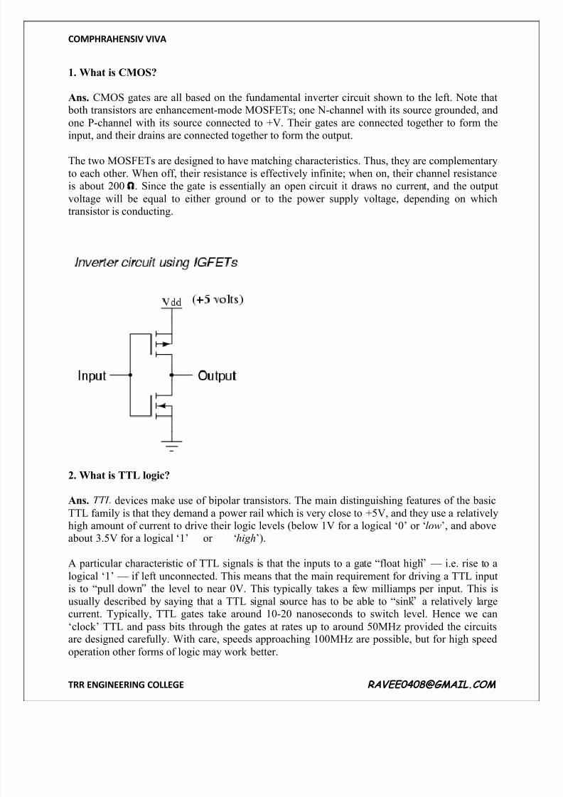
1. What is CMOS?
Ans. CMOS gates are all based on the fundamental inverter circuit shown to the left. Note thatboth transistors are enhancement-mode MOSFETs; one N-channel with its source grounded, and
one P-channel with its source connected to +V. Their gates are connected together to form the
input, and their drains are connected together to form the output.
The two MOSFETs are designed to have matching characteristics. Thus, they are complementary
to each other. When off, their resistance is effectively infinite; when on, their channel resistanceis about 200 . Since the gate is essentially an open circuit it draws no current, and the output
voltage will be equal to either ground or to the power supply voltage, depending on whichtransistor is conducting.
2. What is TTL logic?
Ans. TTL devices make use of bipolar transistors. The main distinguishing features of the basic
TTL family is that they demand a power rail which is very close to +5V, and they use a relativelyhigh amount of current to drive their logic levels (below 1V for a logical µ0¶ or µlow¶, and aboveabout 3.5V for a logical µ1¶ or µhigh¶).
A particular characteristic of TTL signals is that the inputs to a gate ³float high ² i.e. rise to a
logical µ1¶ ² if left unconnected. This means that the main requirement for driving a TTL inputis to ³pull down the level to near 0V. This typically takes a few milliamps per input. This is
usually described by saying that a TTL signal source has to be able to ³sink a relatively largecurrent. Typically, TTL gates take around 10-20 nanoseconds to switch level. Hence we can
µclock¶ TTL and pass bits through the gates at rates up to around 50MHz provided the circuitsare designed carefully. With care, speeds approaching 100MHz are possible, but for high speed
operation other forms of logic may work better.

8/7/2019 jntu ece comprahensiv viva
http://slidepdf.com/reader/full/jntu-ece-comprahensiv-viva 39/87
COMPHRAHENSIV VIVA
TRR ENGINEERING COLLEGE [email protected]
3. What are Functions and Procedures?
Ans. Functions and procedures in VHDL, which are collectively known as subprog rams, aredirectly analogous to functions and procedures in a high-level software programming language
such as C or Pascal. A procedure is a subprogram that has an argument list consisting of inputs
and outputs, and no return value. A function is a subprogram that has only inputs in its argumentlist, and has a return value.
Subprograms are useful for isolating commonly-used segments of VHDL source code. They caneither be defined locally (within an architecture, for example), or they can be placed in a package
and used globally throughout the design description or project.
4. What is Structural design elements?
Ans. A VHDL architecture that uses components is often called a structural description or
Structural design.
The important features of structural type of architecture body are,
Design hierarchyComponents are used
Each component is simulated separatelyIn structural modeling, an entity is described as a set of components connected by signals,
that is, as a net list. The components used in an architecture may be form a library or may beones that were previously defined as part of design.
5. What is a decoder?
Ans. A decoder is a device which does the reverse of an encoder, undoing the encoding so that
the original information can be retrieved. The same method used to encode is usually justreversed in order to decode.
In digital electronics, a decoder can take the form of a multiple-input, multiple-output logic
circuit that converts coded inputs into coded outputs, where the input and output codes aredifferent. e.g. n-to-2
n, binary-coded decimal decoders.
The example decoder circuit would be an AND gate because the output of an AND gate is
"High" (1) only when all its inputs are "High." Such output is called as "active High output". If instead of AND gate, the NAND gate is connected the output will be "Low" (0) only when all its
inputs are "High". Such output is called as "active low output"
6. What is Barrel Shifter?
Ans. A barrel shifter is a digital circuit that can shift a data word by a specified number of bits
in one clock cycle. It can be implemented as a sequence of multiplexers (mux.), and in such an
8/7/2019 jntu ece comprahensiv viva
http://slidepdf.com/reader/full/jntu-ece-comprahensiv-viva 40/87
COMPHRAHENSIV VIVA
TRR ENGINEERING COLLEGE [email protected]
implementation the output of one mux is connected to the input of the next mux in a way thatdepends on the shift distance.
For example, take a 4-bit barrel shifter, with inputs A, B, C and D. The shifter can cycle the
order of the bits ABCD as DABC , CDAB, or BCDA; in this case, no bits are lost. That is, it can
shift all of the outputs up to three positions to the right (and thus make any cyclic combination of A, B, C and D). The barrel shifter has a variety of applications, including being a usefulcomponent in microprocessors.
7. What is a shift register?
Ans. In digital circuits, a shift register is a cascade of flip flops, sharing the same clock, which
has the output of any one but the last flip-flop connected to the "data" input of the next one in thechain, resulting in a circuit that shifts by one position the one-dimensional "bit array" stored in it,
shift ing in the data present at its input and shift ing out the last bit in the array, when enabled to
do so by a transition of the clock input. More generally, a shift register may bemultidimensional, such that its "data in" input and stage outputs are themselves bit arrays: this isimplemented simply by running several shift registers of the same bit-length in parallel.
Shift registers can have both parallel and serial inputs and outputs. These are often configured as
serial-in, parallel-out (SIPO) or as parallel-in, serial-out (PISO). There are also types that haveboth serial and parallel input and types with serial and parallel output. There are also bi-
directional shift registers which allow shifting in both directions: LR or RL. The serialinput and last output of a shift register can also be connected together to create a circular shift
register
8. What is SRAM?
Ans. Static random-access memory (SRAM) is a type of semiconductor memory where the
word st at ic indicates that, unlike d ynamic RAM (DRAM), it does not need to be periodicallyrefreshed, as SRAM uses bistable latching circuitry to store each bit. SRAM exhibits data
remanence, but is still volat ile in the conventional sense that data is eventually lost when thememory is not powered.
SRAM is more expensive, but faster and significantly less power hungry (especially idle) than
DRAM. It is therefore used where either bandwidth or low power, or both, are principalconsiderations. SRAM is also easier to control (interface to) and generally more truly random
access than modern types of DRAM. Due to a more complex internal structure, SRAM is lessdense than DRAM and is therefore not used for high-capacity, low-cost applications such as the
main memory in personal computers.

8/7/2019 jntu ece comprahensiv viva
http://slidepdf.com/reader/full/jntu-ece-comprahensiv-viva 41/87
COMPHRAHENSIV VIVA
TRR ENGINEERING COLLEGE [email protected]
VL SI DESIGN

8/7/2019 jntu ece comprahensiv viva
http://slidepdf.com/reader/full/jntu-ece-comprahensiv-viva 42/87
COMPHRAHENSIV VIVA
TRR ENGINEERING COLLEGE [email protected]
1. What is BiCMOS?
Ans. BiCMOS technology is a combination of Bipolar and CMOS technology. CMOStechnology offers less power dissipation, smaller noise margins, and higher packing density.
Bipolar technology, on the other hand, ensures high switching and I/O speed and good noise
performance. It follows that BiCMOS technology accomplishes both - improved speed over CMOS and lower power dissipation than bipolar technology. The main drawback of BiCMOStechnology is the higher costs due to the added process complexity. Impurity profiles have to be
optimized to both NPN and CMOS issues.
2. What is Bi-CMOS Inverters?
Ans. Two bipolar transistors (T3 and T4), one nMOS and one pMOS transistor (both
enhancement-type devices, OFF at Vin=0V)
The MOS switches perform the logic function & bipolar transistors drive output loads
Vin = 0 :
T1 is off. Therefore T3 is non-conducting
T2 ON - supplies current to base of T4
T4 base voltage set to Vdd.

8/7/2019 jntu ece comprahensiv viva
http://slidepdf.com/reader/full/jntu-ece-comprahensiv-viva 43/87
COMPHRAHENSIV VIVA
TRR ENGINEERING COLLEGE [email protected]
T4 conducts & acts as current source to charge load CL towards Vdd.
Vout rises to Vdd - Vbe (of T4)
Note : Vbe (of T4) is base-emitter voltage of T4.
(pullup bipolar transistor turns off as the output approaches
5V - Vbe (of T4))
Vin = Vdd :
T2 is off. Therefore T4 is non-conducting.
T1 is on and supplies current to the base of T3
T3 conducts & acts as a current sink to discharge load CL towards 0V.
Vout falls to 0V+ VCEsat (of T3)
Note : VCEsat (of T3) is saturation V from T3 collector to emitter.
3. What is Stick diagram?
Ans. Stick diagrams are commonly used to represent the topology (not the geometry) of CMOSintegrated circuits. With a little annotation (FET width and length) they provide adequateinformation to guide layout and mask generation.Stick diagrams help plan layout quickly± Need not be to scale± Draw with color pencils or dry-erase marker
4.Give the basic process for IC fabrication?
Ans. Silicon wafer Preparation
Epitaxial Growth Oxidation
Photolithography Diffusion
Ion Implantation Isolation technique
Metallization
Assembly processing & Packaging5. What are gate primitives?
Ans. Verilog supports basic logic gates as predefined primitives. Primitive logic functionkeyword provide the basics for structural modeling at gate level. These primitives are
instantiated like modules except that they are predefined in verilog and do not need a moduledefinition. The important operations are and, nand, or, xor, xnor, and buf(non-inverting drive
buffer).
8/7/2019 jntu ece comprahensiv viva
http://slidepdf.com/reader/full/jntu-ece-comprahensiv-viva 44/87
COMPHRAHENSIV VIVA
TRR ENGINEERING COLLEGE [email protected]
6. What is a FPGA?
Ans. A field programmable gate array (FPGA) is a programmable logic device that supportsimplementation of relatively large logic circuits. FPGAs can be used to implement a logic circuit
with more than 20,000 gates whereas a CPLD can implement circuits of upto about 20,000
equivalent gates.
7. Write notes on functionality tests?
Ans. Functionality tests verify that the chip performs its intended function. These tests assert that
all the gates in the chip, acting in concert, achieve a desired function. These tests are usually usedearly in the design cycle to verify the functionality of the circuit..
8. What is fault grading?
Ans. Fault grading consists of two steps. First, the node to be faulted is selected. A simulation is
run with no faults inserted, and the results of this simulation are saved. Each node or line to befaulted is set to 0 and then 1 and the test vector set is applied. If and when a discrepancy isdetected between the faulted circuit response and the good circuit response, the fault is said to be
detected and the simulation is stopped.

8/7/2019 jntu ece comprahensiv viva
http://slidepdf.com/reader/full/jntu-ece-comprahensiv-viva 45/87
COMPHRAHENSIV VIVA
TRR ENGINEERING COLLEGE [email protected]
SECTION -III

8/7/2019 jntu ece comprahensiv viva
http://slidepdf.com/reader/full/jntu-ece-comprahensiv-viva 46/87
COMPHRAHENSIV VIVA
TRR ENGINEERING COLLEGE [email protected]
PROBABIL ITY THEORY
AND ST OCHAST IC
PROCESSES

8/7/2019 jntu ece comprahensiv viva
http://slidepdf.com/reader/full/jntu-ece-comprahensiv-viva 47/87
COMPHRAHENSIV VIVA
TRR ENGINEERING COLLEGE [email protected]
1. Define sample space?
Ans. A set of all possible distinct events of a random experiment is known as sample space.
Example:
The sample space, when a dice is thrown is {1, 2, 3, 4, 5, 6}.
2. Define continuous random variable?
Ana. If a random variable µX¶ takes only of finite or all possible values between certain limits, it
is called a continuous random variable.
Example:
Heights, Weights etc.
3. Explain about skew?
Ans. The skew of the density function is a measure of the symmetry of the probability density
function fx(x) of random variable X about x=m1.
The skew of a density function is also called as third central movement of the random
variable and is given by,
µ 3= E[(X-m)3].
4. Define conditional probability mass function?
Ans. If A and B are 2 random variables. The conditional probability mass function (or)
conditional density function of the random variable B, given A=a is,
F(b/a)= f(a/b)/g(a), g(a)>0
Where ,
a,b are arbitrary real numbers
f(a,b) is the joint probability density function
g(a) is marginal density function of A=a.

8/7/2019 jntu ece comprahensiv viva
http://slidepdf.com/reader/full/jntu-ece-comprahensiv-viva 48/87
COMPHRAHENSIV VIVA
TRR ENGINEERING COLLEGE [email protected]
5. Write the properties of Gaussian random variables?
Ans. The properties of Gaussian random variables are given below,
1. The Gaussian random variables are completely defined through only their means, variances
and co-variances.
2. Random variables are said to be statistically independent if they are uncorrelated.
6. Explain the classification of random process?
Ans. Random processes are classified into 4 types according to the characteristics of µt¶ and the
random variable X=X(t) at time t. they are,
i. Continous random process
ii. Discrete random process
iii. Continous random sequence
iv. Discrete random sequence.
7. State any 1 property of PSD?
Ans. For a wide-sense-stationary random process, power spectral density at zero frequency
(=0) gives the area under the graph of auto correlation.
8. What are the different types of noises?
Ans. The various types of noises are,
i. Flicker Noise
ii. Shot Noise
iii. Partition Noise
iv. Thermal Noise.

8/7/2019 jntu ece comprahensiv viva
http://slidepdf.com/reader/full/jntu-ece-comprahensiv-viva 49/87
COMPHRAHENSIV VIVA
TRR ENGINEERING COLLEGE [email protected]
SIGNAL S AND SYST EMS

8/7/2019 jntu ece comprahensiv viva
http://slidepdf.com/reader/full/jntu-ece-comprahensiv-viva 50/87
COMPHRAHENSIV VIVA
TRR ENGINEERING COLLEGE [email protected]
1. What is SIGNALS AND CLASSIFICATION OF SIGNALS?
Ans. A signal is a function representing a physical quantity or variable, and typically it containsinformation about the behavior or nature of the phenomenon. For instance, in a RC circuit thesignal may represent the voltage across the capacitor or the current flowing in the resistor.
Mathematically, a signal is represented as a function of an independent variable t. Usually trepresents time. Thus, a signal is denoted by x(t).
2. What are the Properties of the Convolution Integral?
Ans. The convolution integral has the following properties.
I. C ommutative:
~ ( t * h) ( t )= h ( t )* ~ ( t )
2. Associative:
{ x P )* h l ( 4* h , ( t ) = x ( t )* { h l ( f *) h 2 ( 4)
3. Distributive:
x ( t )* { h , ( t ) )+ h N = x ( t )* h l ( t )+ x ( t )* h, ( t )
3. What are C ausal and S tabl e Syst ems?
Ans. If the system is both causal and stable, then all the poles of H(s) must lie in the left half of
the s-plane; that is, they all have negative real parts because the ROC is of the form Re(s) >amax, and since the jo axis is included in the ROC, we must have a,, < 0.
4. Define Z-Transform?
Ans. The function H(z) in Eq. (4.2) is referred to as the z-transform of h[n]. For a general
discrete-time signal x[n], the z-transform X(z) is defined asm
X (Z)= x[n] z - "
n= -OD
( 4 . 3 )The variable z is generally complex-valued and is expressed in polar form as where r is the
magnitude of z and R is the angle of z . The z-transform defined in is often called the bilateral(or two-sid ed ) z-transform in contrast to the unilateral.
5. Define impulse response of a DT system.
Ans. The impulse response is the output produced by DT system when unit impulse is applied atthe input. The impulse response is denoted by h(n). The impulse response h(n) is obtained by
taking inverse Z transform from the transfer function H(z)
8/7/2019 jntu ece comprahensiv viva
http://slidepdf.com/reader/full/jntu-ece-comprahensiv-viva 51/87
COMPHRAHENSIV VIVA
TRR ENGINEERING COLLEGE [email protected]
6. State Sampling theorem.?
Ans. A band limited signal of finite energy, which has no frequency components higher than the
W hertz, is completely described by specifying the values of the signal at the instant of timeseparated by 1/2W seconds and
A band limited signal of finite energy, which has no frequency components higher than the W
hertz, is completely recovered from the knowledge of its samples taken at the rate of 2W samples
per second.
7. What are the Properties of ROC.?
Ans. i. The ROC of a finite duration sequence includes the entire z- plane,
except z= 0 and z =�.
ii. ROC does not contain any poles.iii. ROC is the ring in the z-plane centered about origin.
iv. ROC of causal sequence (right handed sequence) is of the form z > r.v. ROC of left handed sequence is of the form z < r.
vi. ROC of two sided sequence is the concentric ring in the z plane
8. State convolution property of Z transform?Ans. The convolution property states that if
x1[n]X1(Z) and
x2[n]
X2(Z) thenx1[n] *x2[n]
X1(Z) X2(Z)
That is convolution of two sequences in time domain is equivalent to
multiplication of their Z transforms

8/7/2019 jntu ece comprahensiv viva
http://slidepdf.com/reader/full/jntu-ece-comprahensiv-viva 52/87
COMPHRAHENSIV VIVA
TRR ENGINEERING COLLEGE [email protected]
DIGIT AL SIGNAL
PROCESSING

8/7/2019 jntu ece comprahensiv viva
http://slidepdf.com/reader/full/jntu-ece-comprahensiv-viva 53/87
COMPHRAHENSIV VIVA
TRR ENGINEERING COLLEGE [email protected]
1. W hat is a continuous and discr et e time signal?
Ans.
C ont inuous t ime sig nal : A signal x(t) is said to be continuous if it is defined for all time t.Continuous time signal arise naturally when a physical waveform such as acoustics waveor light wave is converted into a electrical signal. This is effected by means of
transducer.(e.g.) microphone, photocell.Discret e t ime sig nal : A discrete time signal is defined only at discrete instants of time.
The independent variable has discrete values only, which are uniformly spaced. Adiscrete time signal is often derived from the continuous time signal by sampling it at a
uniform rate.
2. W hat ar e time invariant syst ems?
Ans.A system is said to be time invariant system if a time delay or advance of the input signal
leads to an idenditical shift in the output signal. This implies that a time invariant systemresponds idenditically no matter when the input signal is applied. It also satisfies the
conditionR{x( n-k)}=y( n-k).
3. Diff er entiat e between DIT and DIF algorithm
Ans.
DIT ± Time is decimated and input is bi reversed format output in natural order DIF ± Frequency is decimated and input is natural order output is bit reversed
format.
4. Distinguish analog and digital filt ers
Ans. Analog Filter Digital Filter
1. Constructed using active or Consists of elements like adder,
passive components and it is subtractor and delay units and it is
described by a differential described by a difference equation
equation
2. Frequency response can be Frequency response can be
changed by changing the changed by changing the filter
components coefficients
3. It processes and generates Processes and generates digital
analog output output
4. Output varies due to external Not influenced by external
conditions conditions

8/7/2019 jntu ece comprahensiv viva
http://slidepdf.com/reader/full/jntu-ece-comprahensiv-viva 54/87
COMPHRAHENSIV VIVA
TRR ENGINEERING COLLEGE [email protected]
5 . W hat is war ping eff ect?
Ans. For smaller values of w there exist linear relationship between w and .but for larger values
of w the relationship is nonlinear. This introduces distortion in the frequency axis. This effectcompresses the magnitude and phase response. This effect is called warping effect
6 . W rit e the st eps involved in FI R filt er d esign?
Ans. Choose the desired frequency response Hd(w)
Take the inverse Fourier transform and obtain Hd(n) Convert the infinite duration sequence
7 .W hat is the princi pl e of d esigning FI R filt er using fr equency sampling method?
Ans. In frequency sampling method the desired magnitude response is sampled and a linear
phase response is specified .The samples of desired frequency response are defined as DFTcoefficients. The filter coefficients are then determined as the IDFT of this set of samples.
8. List the on-chi p peri pherals in 5X .
Ans. The C5X DSP on-chip peripherals available are as follows:
1. Clock Generator 2. Hardware Timer
3. Software-Programmable Wait-State Generators4. Parallel I/O Ports
5. Host Port Interface (HPI)6. Serial Port
7. Buffered Serial Port (BSP)8. Time-Division Multiplexed (TDM) Serial Port
9. User-Maskable Interrupts

8/7/2019 jntu ece comprahensiv viva
http://slidepdf.com/reader/full/jntu-ece-comprahensiv-viva 55/87
COMPHRAHENSIV VIVA
TRR ENGINEERING COLLEGE [email protected]
DIGIT AL IMAGE
PROCESSING

8/7/2019 jntu ece comprahensiv viva
http://slidepdf.com/reader/full/jntu-ece-comprahensiv-viva 56/87
COMPHRAHENSIV VIVA
TRR ENGINEERING COLLEGE [email protected]
1. Define I mag e?
Ans. An Image may be defined as a two dimensional function f(x,y) where x & y are spatial(plane) coordinates, and the amplitude of f at any pair of coordinates (x,y) is called intensity or
gray level of the image at that point. When x,y and the amplitude values of f are all finite,discrete quantities we call the image as Digital Image.
2. Write the expression of one-dimensional discrete Fourier transforms
Ans. Forward transformThe sequence of x(n) is given by x(n) = { x0,x1,x2,« xN-1}.
X(k) = (n=0 to N-1) _ x(n) exp(-j 2* pi* nk/N) ; k= 0,1,2,«N-1Reverse transformsX(n) = (1/N) (k=0 to N-1) _ x(k) exp(-j 2* pi* nk/N) ; n= 0,1,2,«N-1
3. Write the properties of Hadamard transform
Ans. 1) Hadamard transform contains any one value.
2) No multiplications are required in the transform calculations.4) The no: of additions or subtractions required can be reduced from N^2 to about
Nlog2N
5) Very good energy compaction for highly correlated images.
4. W hat is C hromatic Adoption?
Ans. The hue of a perceived color depends on the adoption of the viewer. For example, the
American Flag will not immediately appear red, white, and blue of the viewer has been subjectedto high intensity red light before viewing the flag. The color of the flag will appear to shift in hue
toward the red component cyan.
5 . H ow the blur is r emoved caused by uniform linear motion?
Ans. An image f(x,y) undergoes planar motion in the x and y-direction and x0(t) and y0(t) arethe time varying components of motion. The total exposure at any point of the recording medium
(digital memory) is obtained by integrating the instantaneous exposure over the time intervalduring which the imaging system shutter is open.
6 . W hat is I mag e T ransform?

8/7/2019 jntu ece comprahensiv viva
http://slidepdf.com/reader/full/jntu-ece-comprahensiv-viva 57/87
COMPHRAHENSIV VIVA
TRR ENGINEERING COLLEGE [email protected]
Ans. An image can be expanded in terms of a discrete set of basis arrays called basisimages. These basis images can be generated by unitary matrices. Alternatively, a
given NXN image can be viewed as an N^2X1 vectors. An image transform provides aset of coordinates or basis vectors for vector space.
7 . N ame the cat egori es of I mag e E nhancement and ex plain?
Ans. The categories of Image Enhancement are1. Spatial domain
2. Frequency domain
Spatial domain: It refers to the image plane, itself and it is based on direct manipulation of pixels of an image.
Frequency domain techniques are based on modifying the Fourier transform of an image.
8. W hat is H uffman C oding ?
Ans. Huffman compression reduces the average code length used to represent the symbols of analphabet. Symbols of the source alphabet, which occur frequently, are assigned with short length
codes. The general strategy is to allow the code length to vary from character to character and toensure that the frequently occurring characters have shorter codes.

8/7/2019 jntu ece comprahensiv viva
http://slidepdf.com/reader/full/jntu-ece-comprahensiv-viva 58/87
COMPHRAHENSIV VIVA
TRR ENGINEERING COLLEGE [email protected]
SECTION -IV

8/7/2019 jntu ece comprahensiv viva
http://slidepdf.com/reader/full/jntu-ece-comprahensiv-viva 59/87
COMPHRAHENSIV VIVA
TRR ENGINEERING COLLEGE [email protected]
ANTENNAS AND WAVE
PROPAGATION

8/7/2019 jntu ece comprahensiv viva
http://slidepdf.com/reader/full/jntu-ece-comprahensiv-viva 60/87
COMPHRAHENSIV VIVA
TRR ENGINEERING COLLEGE [email protected]
1. What is meant by radiation pattern?
Ans. Radiation pattern is the relative distribution of radiated power as a function of distance inspace .It is a graph which shows the variation in actual field strength of the EM wave at all points
which are at equal distance from the antenna. The energy radiated in a particular direction by an
antenna is measured in terms of FIELD STRENGTH.(E Volts/m)
2. What is meant by antenna beam width?
Ans. Antenna beam width is a measure of directivity of an antenna. Antenna beam width is an
angular width in degrees, measured on the radiation pattern (major lobe) between points wherethe radiated power has fallen to half its maximum value .This is called as ³beam width between
half power points or half power beam width.(HPBW).
3.What is meant by uniform linear array.?
Ans. An array is linear when the elements of the array are spaced equally along the straight line.If the elements are fed with currents of equal magnitude and having a uniform progressive phase
shift along the line, then it is called uniform linear array .
4. List the applications of helical antenna?
Ans. The applications of helical antenna are:
It became the workhouse of space communications for telephone,television and data, being employed both on satellites and at ground
stations
Many satellites including weather satellites, data relay satellites all havehelical antennas
It is on many other probes of planets and comets, including moon and
mars, being used alone, in arrays or as feeds for parabolic reflectors, itscircular polarization and high gain and simplicity making it effective for
space application
5. What is meant by Space Wave.?
Ans. It is made up of direct wave and ground reflected wave. Also includes the portion of energy
received as a result of diffraction around the earth surface and the reflection from the upper atmosphere

8/7/2019 jntu ece comprahensiv viva
http://slidepdf.com/reader/full/jntu-ece-comprahensiv-viva 61/87
COMPHRAHENSIV VIVA
TRR ENGINEERING COLLEGE [email protected]
6. What is meant by Faraday¶ s rotation?
Ans. Due to the earth¶ s magnetic fields, the ionosphere medium becomes anisotropic and theincident plane wave entering the ionosphere will split into ordinary and extra ordinary
waves/modes. When these modes re-emerge from the ionosphere they recombine into a single
plane wave again. Finally the plane of polarization will usually have changed, this phenomenonis known as Faraday¶ s rotation.
7. Define LUHF?
Ans. The lowest useful HF for a given distance and transmitter power is defined as the lowestfrequency that will give satisfactory reception for that distance and power.
It depends on The effective radiated power
Absorption character of ionosphere for the paths between transmitter and receiver. The required field strength which in turn depends upon the radio noise at the
receiving location and type of service involved .
8. Define skip distance & Optimum frequency.?
Ans.
SKIP DISTANCEThe distance with in which a signal of given frequency fails to be reflected back is the skip
distance for that frequency. The higher the frequency the greater the skip distance.
OPTIMUM FREQUENCY
Optimum frequency for transmitting between any two points is therefore selected as somefrequency lying between about 50 and 85 percent of the predicted maximum usable frequency
between those points.
8/7/2019 jntu ece comprahensiv viva
http://slidepdf.com/reader/full/jntu-ece-comprahensiv-viva 62/87
COMPHRAHENSIV VIVA
TRR ENGINEERING COLLEGE [email protected]
MICROWAVE
ENGINEERING
1. Define s-matrix

8/7/2019 jntu ece comprahensiv viva
http://slidepdf.com/reader/full/jntu-ece-comprahensiv-viva 63/87
COMPHRAHENSIV VIVA
TRR ENGINEERING COLLEGE [email protected]
Ans. In a microwave junction there is intersection of three or more components. There will be an
output port ,in addition there may be reflection from the junction of other ports. Totally theremay be many combinations, these are represented easily using a matrix called S matrix
2. What are ferrites and give its properties?
Ans. Ferrites are ceramic like materials. These are made by by sintering a mixture of metallic
oxides.
Properties Specific resistivity is may be used as much as 1014 greater than that of metals
Dielectric constants around 10to 15 or greater Relative permeability is 1000
3.What is Faraday¶s rotation law?
Ans. If a circularly polarized wave is made to pass through a ferrite rod which has beeninfluenced by an axial magnetic field B ,then the axis of polarization gets tilted in clockwise
direction and amount of tilt depends upon the strength of magnetic field and geometry of theferrite
4. What are the assumptions for calculation of RF power in Reflex Klystron?
Ans. i) Cavity grids and repeller are plane parallel and very large in extent.
ii) No RF field is excited in repeller space
iii) Electrons are not intercepted by the cavity anode grid.iv) No debunching takes place in repeller space.
v) The cavity RF gap voltage amplitude V, is small compared to the dc beamvoltage VO
5. Dicuss the high frequency effects in conventional tubes?
Ans. The high frequency effects in conventional tubes arei) Circuit reactance
a)Inter electrode capacitanceb) Lead inductance
ii) Transit time effectiii) Cathode emission
iv) Plate heat dissipation areav) Power loss due to skin effect, radiation and dielectric loss
6. What is the purpose of slow wave structures used in TWT amplifiers?

8/7/2019 jntu ece comprahensiv viva
http://slidepdf.com/reader/full/jntu-ece-comprahensiv-viva 64/87
COMPHRAHENSIV VIVA
TRR ENGINEERING COLLEGE [email protected]
Ans. Slow wave structures are special circuits that are used in microwave tubes to reduce wave
velocity in a certain direction so that the electron beam and the signal wave can interact. InTWT, since the beam can be accelerated only to velocities that are about a fraction of the
velocity of light, slow wave structures are used.
7. What are the applications of TRAPATT devices?
Ans. The applications are
a)Phased-array Radar systemsb)Intermediate frequency transmitters.
c)Proxity fuse sourcesd)Radio altimeters
e)Microwave landing systems.
8.What is negative resistance in gunn diode?
Ans. The carrier drift velocity increases linearly from 0 to maximum when the electric field is
increased from 0 to threshold value in gunn diodes. When the electric field is beyond thethreshold value of 3000v/cm the drift velocity is decreased and the diode exhibit negative
resistance.

8/7/2019 jntu ece comprahensiv viva
http://slidepdf.com/reader/full/jntu-ece-comprahensiv-viva 65/87
COMPHRAHENSIV VIVA
TRR ENGINEERING COLLEGE [email protected]
OPT ICAL COMMUN ICAT ION
1. Define Numerical aperture of a step index fiber?

8/7/2019 jntu ece comprahensiv viva
http://slidepdf.com/reader/full/jntu-ece-comprahensiv-viva 66/87
COMPHRAHENSIV VIVA
TRR ENGINEERING COLLEGE [email protected]
Ans. Numerical aperture (N.A) of the fiber is the light collecting efficiency of the fiber and is themeasure of the amount of light rays that can be accepted by the fiber. It is equal to the sine of
acceptance.
N.A= n0 sin 0max = (n12
- n22)
1/2
where n1 and n2 are the refractive indices of core and cladding respectively.
2. What are the uses of optical fibers?
Ans.a) To transmit the information which are in the form of coded signals of the
telephone communication, computer data, etc.b) To transmit the optical images (Example : Endoscopy)
c) To act as a light source at the inaccessible places.d) To act as sensors to do mechanical, electrical and magnetic measurements
3. What is Guide dispersion?
Ans. Wave guide dispersion which occurs because of a single mode fiber confines only about80% of optical power to the core. Dispersion this arises since 20% of light propagates in
cladding travels faster than the light confined to the core. Amount of wave-guide dispersiondepends on fiber design. Other factor for pulse spreading is inter modal delay
4. Give an account on single mode lasers and modulation of laser diodes.?
Ans.
Single mode lasers:
It is used for long-distance communication.
It consists of a single longitudinal mode and single transverse mode.The spectral width is low.
Al t ernat ive devices developed are
1. Vertical cavity surface emitting lasers
2. Structures that have a built-in frequency-selective grating.3. Tunable lasers.
5. Define direct band gap materials and indirect band gap materials.?
Ans.

8/7/2019 jntu ece comprahensiv viva
http://slidepdf.com/reader/full/jntu-ece-comprahensiv-viva 67/87
COMPHRAHENSIV VIVA
TRR ENGINEERING COLLEGE [email protected]
Direct band gap: In direct band gap materials direct transition is possible from valence band to conduction band.
e.g. GaAs, InP, InGaAs
Indirect band gap: In indirect band gap materials direct transition is not possible from valence band to conduction.
e.g. silicon, germanium.
6. Define internal quantum efficiency.
Ans. The internal quantum efficiency is the fraction of the electron-hole pairs that recombineradiatively.If the radiative recombination rate is R and the non radiative recombination rate is
Rnr, then the internal quantum efficiency is the ratio of the ratio of the radiative recombinationrate to the total recombination rate
7. What is meant by µpopulation inversion¶?
Ans. In thermal equilibrium, the density of excited electrons is very small. Most photons incidenton the system will therefore be absorbed, so that stimulated emission is essentially negligible.
Stimulated emission will exceed absorption only if the population of the excited states is greater than that of the ground state. This condition is known as population inversion.
8. Write in detail about avalanche photodiodes and explain briefly about photo detector
noise and SNR?
Ans.
Avalanche photodiodesa. Impact ionization
b. Avalanche effectc. Reach-through construction
d. p+ _ p n+ reach- through structuree. Principle of reach through
f. Ionization rate
Photo detector noiseSNR at output of an optical receiver
Condition to achieve a high SNR SNR
S = (ip2)M2N 2q(Ip+ID)M2F(M)+2qILB+4KBTB/RL

8/7/2019 jntu ece comprahensiv viva
http://slidepdf.com/reader/full/jntu-ece-comprahensiv-viva 68/87
COMPHRAHENSIV VIVA
TRR ENGINEERING COLLEGE [email protected]
EM WAVES AND
T RANSMISSION L INES
1. Define conductivity of a material?

8/7/2019 jntu ece comprahensiv viva
http://slidepdf.com/reader/full/jntu-ece-comprahensiv-viva 69/87
COMPHRAHENSIV VIVA
TRR ENGINEERING COLLEGE [email protected]
Ans. According to the Ohms laws, conductivity defined as the current density per unit electricfield. Based upon conductivity materials classified into two types,
1. Conductors2. Non-conductors.
Conductivity of the material depends upon the frequency and temperature.
2. Define magnetic flux density?
Ans. Magnetic flux constitutes the magnetic lines of force produced by a permanent magnet or a
current carrying conductor. In case of current carrying conductor, the magnetic lines of forcesurround the conductor to form concentric circles and they do not intersect each other.
3. Explain faraday's law for time varying fields?
Ans. Faraday's first law of electromagnetic induction states that "When ever the number of magnetic lines of force (called as magnetic flux) passing through a conductor changes, an e.m.f
is induced in it".Faraday's second law of electromagnetic induction states that "The magnetic of the
induced e.m.f. is proportional to the rate of change of magnetic lines of force".
4. What is meant by the polarization of wave?
Ans. By definition, the polarization of a wave is the locus of the tip of the electric field at a given
point as a function of time. When two or more waves of the same frequency propagate in thesame direction.
5. Define plane of incidence?
Ans. If the wave travel through one medium and then enters another medium of infinite extentand is assumed that the interface between the two media is normal to the direction of propagation
of the incoming wave is called the incident wave and the medium in which this waves travels iscalled plane of incidence.
6. Explain the term "conduction current"?
Ans. It is the current caused by the applied electric field to any conductor, A.A current through aresistive element is called conduction current. If a constant potential difference is applied across
a conductor produces a continuous flow of current of constant value can be termed as conductioncurrent.

8/7/2019 jntu ece comprahensiv viva
http://slidepdf.com/reader/full/jntu-ece-comprahensiv-viva 70/87
COMPHRAHENSIV VIVA
TRR ENGINEERING COLLEGE [email protected]
7. Define reflection coefficient?
Ans. It is the ratio of reflected to incident electric field strength. Reflection coefficient hasdifferent values for both parallel and perpendicular polarization.
8. What are equi-potential surfaces?
Ans. If the potential throughout the surface is same, then such surface is referred as equi-potential surface. The line intersection of an equi-potential surface and a plane results
in a path or line known as an equi-potential line.

8/7/2019 jntu ece comprahensiv viva
http://slidepdf.com/reader/full/jntu-ece-comprahensiv-viva 71/87
COMPHRAHENSIV VIVA
TRR ENGINEERING COLLEGE [email protected]
SECTION -V

8/7/2019 jntu ece comprahensiv viva
http://slidepdf.com/reader/full/jntu-ece-comprahensiv-viva 72/87
COMPHRAHENSIV VIVA
TRR ENGINEERING COLLEGE [email protected]
RADAR SYST EMS
1. Give the Radar equation?
Ans. The power P r returning to the receiving antenna is given by the radar equation:

8/7/2019 jntu ece comprahensiv viva
http://slidepdf.com/reader/full/jntu-ece-comprahensiv-viva 73/87
COMPHRAHENSIV VIVA
TRR ENGINEERING COLLEGE [email protected]
where
P t = transmitter power
Gt = gain of the transmitting antenna
Ar = effective aperture (area) of the receiving antenna
= radar cross section, or scattering coefficient, of the target
F = pattern propagation factor
Rt = distance from the transmitter to the target
Rr = distance from the target to the receiver.
In the common case where the transmitter and the receiver are at the same
location, Rt = Rr and the term Rt Rr can be replaced by R4, where R is the range. This
yields:
2. W rit e short not es about N oise in Radar?
Ans. Signal noise is an internal source of random variations in the signal, which is generated by
all electronic components. Noise typically appears as random variations superimposed on thedesired echo signal received in the radar receiver. The lower the power of the desired signal, the
more difficult it is to discern it from the noise (similar to trying to hear a whisper while standing
near a busy road). Noise figure is a measure of the noise produced by a receiver compared to an
ideal receiver, and this needs to be minimized.
Noise is also generated by external sources, most importantly the natural thermal radiation of the
background scene surrounding the target of interest. In modern radar systems, due to the high
performance of their receivers, the internal noise is typically about equal to or lower than the
external scene noise. An exception is if the radar is aimed upwards at clear sky, where the scene
is so "cold" that it generates very little thermal noise.
3. What isDoppler effect?
Ans. Ground-based radar systems used for detecting speeds rely on the Doppler effect. The
apparent frequency (f) of the wave changes with the relative position of the target. The Doppler

8/7/2019 jntu ece comprahensiv viva
http://slidepdf.com/reader/full/jntu-ece-comprahensiv-viva 74/87
COMPHRAHENSIV VIVA
TRR ENGINEERING COLLEGE [email protected]
equation is stated as follows for vobs (the radial speed of the observer) and vs (the radial speed of
the target) and f 0 frequency of wave :
4. What is FM ± CW RADAR?
Ans. Frequency Modulated Continuous-wave radar is a short range measuring radar set. This
kind of radar is often used as ³radar altimeter to measure the exact height during the landing
procedure of aircraft
FMCW) is a radar system where a known stable frequency wave radio energy is
modulated by a triangular modulation signal so that it varies gradually and then mixes
with the signal reflected from a target object with this transmit signal to produce a beat
signal.
5. What is MTI Radar?
Ans. MTI radars introduce additional loss. The MTI discrimination technique results in
complete loss of sensitivity for certain target values (blind speeds) In a radar with overlapping range gates, the gates may be wider than optimum for
practical reasons. The additional noise introduced by non ± optimum gate width leads to
degradation performance. Straddling loss accounts for loss in SNR for targets not at the centre of a range
gate, or at the centre of a filter in a multiple bank processor
6. What is RADAR ttrack extraction?
Ans. Radar video returns on aircraft can be subjected to a plot extraction process whereby
spurious and interfering signals are discarded. A sequence of target returns can be monitored
through a device known as a plot extractor. The non relevant real time returns can be removed
from the displayed information and a single plot displayed. In some radar systems, or
alternatively in the command and control system to which the radar is connected, a radar
tracker is used to associate the sequence of plots belonging to individual targets and estimate the
targets' headings and speeds.

8/7/2019 jntu ece comprahensiv viva
http://slidepdf.com/reader/full/jntu-ece-comprahensiv-viva 75/87
COMPHRAHENSIV VIVA
TRR ENGINEERING COLLEGE [email protected]
7. Reduction of interference effects in Radar?
Ans. Signal processing is employed in radar systems to reduce the radar interference effects.
Signal processing techniques include moving target indication (MTI), pulse Doppler, moving
target detection (MTD) processors, correlation with secondary surveillance radar (SSR)
targets, space-time adaptive processing (STAP), and track-before-detect (TBD). Constant false
alarm rate (CFAR) and digital terrain model (DTM) processing are also used in clutter
environments
8. What are the requirements of Radar receiver?
Ans. The ideal radar receiver is required to:
y
amplify the received signals without adding noise or introducing any form of distortion;y optimise the probability of detection of the signal by its bandwidth characteristics.
y provide a large dynamic range to accommodate large clutter signals;
y reject interfering signals so that the required information can be optimally detected.
.

8/7/2019 jntu ece comprahensiv viva
http://slidepdf.com/reader/full/jntu-ece-comprahensiv-viva 76/87
COMPHRAHENSIV VIVA
TRR ENGINEERING COLLEGE [email protected]
ANAL OG
COMMUN ICAT IONS
8/7/2019 jntu ece comprahensiv viva
http://slidepdf.com/reader/full/jntu-ece-comprahensiv-viva 77/87
COMPHRAHENSIV VIVA
TRR ENGINEERING COLLEGE [email protected]
1. What is the need for modulation?
Ans. Mainly to decrease the antenna size
to increase the bandwidth of the signal to multiplex the signals
to reduce the interference made when we transmit the signals with nearly samefrequency in the audio frequency range (20-20k)kHz.
to favour the complexity of the transmission system
2. What is Costas Loop?
Ans. A Costas loop is a phase-locked loop used for carrier phase recovery from suppressed-
carrier modulation signals, such as from double-sideband suppressed carrier signals. The primary
application of Costas loops is in wireless receivers. Its advantage over the PLL-based detectors is
that at small deviations the Costas loop error voltage is sin(2( ií
f )) vs sin(
ií
f ). This translates
to double the sensitivity and also makes the Costas loop uniquely suited for tracking Doppler-
shifted carriers esp. in OFDM and GPS.
3. What is SSB?
Ans. Single-sideband modulation (SSB) is a refinement of amplitude modulation that moreefficiently uses electrical power and bandwidth. It is closely related to vestigial sidebandmodulation (VSB)
Amplitude modulation produces a modulated output signal that has twice the bandwidth of the
original baseband signal. Single-sideband modulation avoids this bandwidth doubling, and thepower wasted on a carrier, at the cost of somewhat increased device complexity.
4. What is FM?
Ans. Frequency modulation (FM) conveys information over a carrier wave by varying its
instantaneous frequency. This is in contrast with amplitude modulation, in which the amplitude
of the carrier is varied while its frequency remains constant. In analog applications, the
difference between the instantaneous and the base frequency of the carrier is directly
proportional to the instantaneous value of the input signal amplitude. Digital data can be sent byshifting the carrier's frequency among a set of discrete values, a technique known as frequency-
shift keying.
FM is widely used for broadcasting of music and speech, and in two-way radio systems
8/7/2019 jntu ece comprahensiv viva
http://slidepdf.com/reader/full/jntu-ece-comprahensiv-viva 78/87
COMPHRAHENSIV VIVA
TRR ENGINEERING COLLEGE [email protected]
5. Noise in Analog communication?
Ans. Analog systems are less tolerant to noise, make good use of bandwidth, and are easy to
manipulate mathematically. However, analog signals require hardware receivers and transmitters
that are designed to perfectly fit the particular transmission. If you are working on a new system,
and you decide to change your analog signal, you need to completely change your transmittersand receivers.
6. What is a Radio transmitter?
Ans. Radio transmitter is an electronic device which, with the aid of an antenna, produces radio
waves. The transmitter itself generates a radio frequency alternating current, which is applied to
the antenna. When excited by this alternating current, the antenna radiates radio waves. In
addition to their use in broadcasting, transmitters are necessary component parts of many
electronic devices that communicate by radio.
7. What is a Radio receiver?
Ans. A radio receiver is an electronic circuit that receives its input from an antenna, uses
electronic filters to separate a wanted radio signal from all other signals picked up by this
antenna, amplifies it to a level suitable for further processing, and finally converts through
demodulation and decoding the signal into a form usable for the consumer, such as sound,
pictures, digital data, measurement values, navigational positions, etc
8. What is TDM?
Ans. Time-division multiplexing (TDM) is a method of putting multiple data streams in a singlesignal by separating the signal into many segments, each having a very short duration. Each
individual data stream is reassembled at the receiving end based on the timing.
The circuit that combines signals at the source (transmitting) end of a communications link is
known as a multiplexer. It accepts the input from each individual end user, breaks each signal
into segments, and assigns the segments to the composite signal in a rotating, repeatingsequence.

8/7/2019 jntu ece comprahensiv viva
http://slidepdf.com/reader/full/jntu-ece-comprahensiv-viva 79/87
COMPHRAHENSIV VIVA
TRR ENGINEERING COLLEGE [email protected]
DIGIT AL
COMMUN ICAT IONS

8/7/2019 jntu ece comprahensiv viva
http://slidepdf.com/reader/full/jntu-ece-comprahensiv-viva 80/87
COMPHRAHENSIV VIVA
TRR ENGINEERING COLLEGE [email protected]
1. What are the advantages of digital communication?
Ans. 1. Digital communication is fast and easier.
2. The transmission quality is very high and almost independent of the distance amongthe terminals.
3. We can increase the capacity for transmission system.
4. The newer types of transmission media such as light beams optical fibers and waveguides operating in the microwave frequency extensively use digital communication.
5. Consistent communication: Very less sensitivity to changes in environmentalconditions (temperature and so on.)
6. Then signaling also very easy.
2. What is delta modulation?
Ans. Delta modulation (DM or -modulation)is an analog-to-digital and digital-to-analog signal
conversion technique used for transmission of voice information where quality is not of primary
importance. DM is the simplest form of differential pulse-code modulation (DPCM where the
difference between successive samples is encoded into n-bit data streams. In delta modulation,
the transmitted data is reduced to a 1-bit data stream. Its main features are:
y the analog signal is approximated with a series of segmentsy each segment of the approximated signal is compared to the original analog wave to
determine the increase or decrease in relative amplitude
y the decision process for establishing the state of successive bits is determined by thiscomparison
3. What is QPSK?
Ans. QPSK, which stands for Quadrature Phase Shift Keying, refers to a type of phasemodulation algorithm where there are four states involved. These four states also refer to four
phases wherein a particular carrier is sent to QPSK. These states consist of 45, 135, 225, and 315degrees.
QPSK is an algorithm providing procedures used in calculating and finding a specific value.
With regards to its encoding, QPSK is capable of processing two bits for each symbol. This isdue to the fact that QPSK has four possible states.
QPSK is applied extensively on certain systems. It can be used to maintain the data rate whileensuring that the bandwidth of the signal is stable. This enables the system to efficiently utilize
its bandwidth resources.

8/7/2019 jntu ece comprahensiv viva
http://slidepdf.com/reader/full/jntu-ece-comprahensiv-viva 81/87
COMPHRAHENSIV VIVA
TRR ENGINEERING COLLEGE [email protected]
4. What is baseband signal?
Ans. A baseband signal converter device for an impulse radio receiver combines multipleconverter circuits and an RF amplifier in a single integrated circuit package. Each converter
circuit includes an integrator circuit that integrates a portion of each RF pulse during a sampling
period triggered by a timing pulse generator. The integrator capacitor is isolated by a pair of Schottky diodes connected to a pair of load resistors. A current equalizer circuit equalizes thecurrent flowing through the load resistors when the integrator is not sampling. Current steering
logic transfers load current between the diodes and a constant bias circuit depending on whether a sampling pulse is present.
5. Define Shannon¶s Entropy?
Ans. Shannon's entropy represents an absolute limit on the best possible lossless compression of any communication, under certain constraints: treating messages to be encoded as a sequence of
independent and identically-distributed random variables, Shannon's source coding theorem
shows that, in the limit, the average length of the shortest possible representation to encode themessages in a given alphabet is their entropy divided by the logarithm of the number of symbolsin the target alphabet.
6. Define Shannon¶s Theorem?
Ans. A given communication system has a maximum rate of information C known as the
channel capacit y.If the information rate R is less than C , then one can approach arbitrarily small error
probabilities by using intelligent coding techniques.To get lower error probabilities, the encoder has to work on longer blocks of signal data.
This entails longer delays and higher computational requirements.
7. What is linear block codes?
Ans. If more error-correcting bits are included with a message, and if those bits can be arranged
such that different incorrect bits produce different error results, then bad bits could be identified.In a 7-bit message, there are seven possible single bit errors, so three error control bits could
potentially specify not only that an error occurred but also which bit caused the error
8. What is Convolutional Codes?
Ans. This chapter describes the encoder and decoder structures for convolutional codes. Theencoder will be represented in many different but equivalent ways. Also, the main decoding
strategy for convolutional codes, based on the Viterbi Algorithm, will be described. A firmunderstanding of convolutional codes is an important prerequisite to the understanding of turbo
codes.

8/7/2019 jntu ece comprahensiv viva
http://slidepdf.com/reader/full/jntu-ece-comprahensiv-viva 82/87
COMPHRAHENSIV VIVA
TRR ENGINEERING COLLEGE [email protected]
T EL ECOMMUN ICAT ION
SWIT CHING SYST EMS

8/7/2019 jntu ece comprahensiv viva
http://slidepdf.com/reader/full/jntu-ece-comprahensiv-viva 83/87
COMPHRAHENSIV VIVA
TRR ENGINEERING COLLEGE [email protected]
1. Principles of cross bar switching?
Ans. A crossbar swit ch (also known as cross-point switch, crosspoint switch, or matrix
switch) is a switch connecting multiple inputs to multiple outputs in a matrix manner. Originally
the term was used literally, for a matrix switch controlled by a grid of crossing metal bars, and
later was broadened to matrix switches in general. It is one of the principal switch architectures,together with a memory switch and a crossover switch.
2. What is Electronic space division switching?
Ans. All the automatic telephone switches, both electromechanical and electronic, discussed up
to this point are classified as space-division switches. Space-division switches are characterized
by the fact that the speech path through a telephone switch is continuous throughout the
exchange. That speech path is a metallic circuit, in the sense that it is provided entirely through
the metallic.
3. What is Subscriber loop systems?
Ans. S ubscriber Loop C arrier (SLC - commonly pronounced "slick") refers to equipment
providing central office-like telephone interface functionality. The SLC Remote Terminal (RT)
is typically located in a remote (from the telephone company central office) area with a high
density of telephone service such as a residential neighborhood. Two or four T1 circuits
(depending on the configuration) connect the SLC RT back to the Central Office Terminal
(COT) in the case of a Universal Subscriber Loop Carrier (USLC). An Integrated Subscriber
Loop Carrier (ISLC) has its T-spans terminating directly in time division switching equipment in
the telephone exchange.
4. What is Grade of service and blocking probability?
Ans. Grade of service is the probability of a call in a circuit g roup being blocked or delayed for more than a specified interval, expressed as a vulgar fraction or decimal fraction. This is always
with reference to the busy hour when the traffic intensity is the greatest. Grade of service may beviewed independently from the perspective of incoming versus outgoing calls, and is not
necessarily equal in each direction or between different source-destination pairs.
5. Define network architecture?
Ans. N et wor k archit ect ure is the design of a communications network. It is a framework for thespecification of a network's physical components and their functional organization andconfiguration, its operational principles and procedures, as well as data formats used in its
operation.
In telecommunication, the specification of a network architecture may also include a detaileddescription of products and services delivered via a communications network, as well as detailed
rate and billing structures under which services are compensated.
8/7/2019 jntu ece comprahensiv viva
http://slidepdf.com/reader/full/jntu-ece-comprahensiv-viva 84/87
COMPHRAHENSIV VIVA
TRR ENGINEERING COLLEGE [email protected]
6. What is OSI model?
Ans. The Open S yst ems I nt erconnect ion model ( OS I model ) is a product of the Open Systems
Interconnection effort at the International Organization for Standardization. It is a way of sub-
dividing a communications system into smaller parts called layers. A layer is a collection of
similar functions that provide services to the layer above it and receives services from the layer below it. On each layer, an inst ance provides services to the instances at the layer above and
requests service from the layer below.
7. What is ISDN?
Ans. I nt eg rat ed S ervices Dig it al N et wor k ( I S DN ) is a set of communications standards for
simultaneous digital transmission of voice, video, data, and other network services over the
traditional circuits of the public switched telephone network
ISDN is a circuit-switched telephone network system, which also provides access to packet
switched networks, designed to allow digital transmission of voice and data over ordinary
telephone copper wires, resulting in potentially better voice quality than an analog phone can
provide. It offers circuit-switched connections (for either voice or data), and packet-switched
connections (for data), in increments of 64 kilobit/s. A major market application for ISDN in
some countries is Internet access, where ISDN typically provides a maximum of 128 kbit/s in
both upstream and downstream directions. Channel bonding can achieve a greater data rate;
typically the ISDN B-channels of 3 or 4 BRIs (6 to 8 64 kbit/s channels) are bonded.
8. What is cable modem?
Ans. A cable modem is a type of network bridge and modem that provides bi-directional data
communication via radio frequency channels on a HFC and RFoG infrastructure. Cable modems
are primarily used to deliver broadband Internet access in the form of cable Internet, taking
advantage of the high bandwidth of a HFC and RFoG network. They are commonly deployed in
Australia, Europe, Asia and Americas
Hybrid fiber -coaxial ( HF C ) is a telecommunications industry term for a broadband network
which combines optical fiber and coaxial cable.
Radio F r equency over G lass (RFoG) is a deep fiber network design in which the coax portion of
the HFC network is replaced by a single-fiber, passive optical architecture (PON)

8/7/2019 jntu ece comprahensiv viva
http://slidepdf.com/reader/full/jntu-ece-comprahensiv-viva 85/87
COMPHRAHENSIV VIVA
TRR ENGINEERING COLLEGE [email protected]
CELL UL AR AND MOBIL E
COMMUN ICAT IONS

8/7/2019 jntu ece comprahensiv viva
http://slidepdf.com/reader/full/jntu-ece-comprahensiv-viva 86/87
COMPHRAHENSIV VIVA
TRR ENGINEERING COLLEGE [email protected]
1. What is Cellular network?
Ans. A cellular network is a radio network distributed over land areas called cells, each served
by at least one fixed-location transceiver known as a cell site or base station. When joined
together these cells provide radio coverage over a wide geographic area. This enables a large
number of portable transceivers (e.g., mobile phones, pagers, etc.) to communicate with eachother and with fixed transceivers and telephones anywhere in the network, via base stations, even
if some of the transceivers are moving through more than one cell during transmission
2. What are the elements in Cellular Mobile Radio System Design?
Ans. Elements of Cellular Mobile Radio System Design
(1) the concept of frequency reuse channels
(2) the co-channel interference reduction factor
(3) the desired carrier -to-interference ratio
(4) the handoff mechanism
(5) cell splitting.
3. What is co channel interference?
Ans. Co-channel interference with a desired signal in a receiver arrangement of a TDMA cellular
radio communications system having two antennas and receivers for providing two received
signals is reduced. Two sampled signals are derived from each of the two received signals by
sampling the respective received signal at twice the symbol rate of the system and separating
alternate samples at twice the symbol rate to produce the two sampled signals each with different
samples at the symbol rate, providing a total of four sampled signals from the two antennas.These signals are linearly combined with respective weights to produce an output signal, the
weights being determined to reduce co-channel interference with the desired signal represented
by the output signal.
4. Discuss the merits of point-to-point model?Ans. 1.The point-to-point provides a more accurate path loss data, while the area-to-area model
provides data with 8 bD in case of point-to-point model.2.The point-to-point prediction model can generate signal coverage maps, interference area
maps, hands-off occurrence maps.
5. What is Omni directional antenna?
Ans. An omnidirectional antenna is an antenna which radiates power uniformly in one plane,
with the radiated power decreasing with elevation angle above or below the plane, dropping to
zero on the antenna's axis. Omnidirectional antennas are widely used for radio broadcasting
antennas, and in mobile devices that use radio such as cell phones, FM radios, walkie-talkies,

8/7/2019 jntu ece comprahensiv viva
http://slidepdf.com/reader/full/jntu-ece-comprahensiv-viva 87/87
COMPHRAHENSIV VIVA
Wifi, cordless phones, GPS as well as for base stations that communicate with mobile radios,
such as police and taxi dispatchers and aircraft communications.
6. What is Channel allocation?
Ans. In TDMA and FDMA based cellular radio systems and wireless networks, channel
allocation schemes are required to allocate channels to base stations and access points and to
avoid co-channel interference among nearby cells. A number of approaches have been tried to
assign bandwidth to users in an efficient manner while minimizing interference to other users.
7. What is cell splitting?
Ans. Cell splitting is one of the concept used to improve the utilization of spectrum efficiency.
When the traffic density is more in the system then the frequency channel present in a cell unitprovide enough mobile calls, hence the original call be split into smaller cells, which is known ascell splitting.
8. What are GSM channels?
Ans. GSM provides a number of different types of channels for user traffic and signaling.
These channels are divided into two classes:
1. Traffic channels
2. Signaling channels