Embed Size (px)
Citation preview

July 2016
Plasma Science and Fusion Center Massachusetts Institute of Technology
Cambridge MA 02139 USA This work is supported by US DOE award DE-SC00-02060. This work made use of the MRSEC Shared Experimental Facilities at MIT, supported by the National Science Foundation under award number DMR-08-19762. Reproduction, translation, publication, use and disposal, in whole or in part, by or for the United States government is permitted.
PSFC/JA-16-27
Isolated nano-tendril bundles on tungsten surfaces exposed to radiofrequency helium plasma
Kevin B. Woller, Dennis G. Whyte, Graham M. Wright

P1.80
1
Isolated nano-tendril bundles on tungsten surfaces exposed to
radiofrequency helium plasma
Kevin B. Woller*, Dennis G. Whyte, Graham M. Wright
MIT Plasma Science and Fusion Center MIT, 175 Albany St., Cambridge, MA, USA, 02139
Abstract:
The DIONISOS experiment is used to study the impact of RF helium (He) plasma on the
surface morphology of tungsten (W). Modulation of incident He ion energy with a span on the
order of 50 eV and below the sputtering threshold at a frequency of 13.56 MHz results in
nano-tendril bundles (NTBs) and free-standing W whiskers on the surface at 1020 K. The
NTBs are distributed intragranularly with coverage of less than 10% while reaching up to 30
microns normal to the surface for He ion fluence of 5.8x1025
m-2
and a flux density of
1.0x10²²
m-2
s-1
. Analysis of the NTB interior and sub-surface structure is provided through
focussed ion beam cross section.
Keywords: tungsten fuzz, helium, nano-tendril, RF sheath
*Corresponding author address: MIT Plasma Science and Fusion Center, 175 Albany St.,
NW17-210, Cambridge, MA, USA, 02139
*Corresponding author e-mail: [email protected]
Presenting author: Kevin B. Woller

P1.80
2
1. Introduction
Tungsten (W) nano-tendrils might occur in future fusion energy devices, especially with
evidence of the growth of nano-tendrils in the high-power density tokamak experiment
Alcator C-MOD [1]. The surface morphology impacts the plasma-surface interactions [2] and
plasma-facing component (PFC) properties [3]. Research is on-going to understand the
fundamental physical mechanisms that drive nano-tendril (metal whiskers that contain He
bubbles) and fuzz (a porous layer of intertwining nano-tendrils) growth. There are two basic
mechanisms for modelling W fuzz growth: pressure driven deformation [4–6] by high
pressure He bubbles (PHe ≳1 GPa) or surface diffusion [7,8] through ion-induced adatoms
(adsorbed atoms) or viscous flow [9]. Adatoms in these models are W surface atoms that have
been pushed onto the surface either by He impregnation of the surface or by the He ions
directly. Through measurements of the He concentration during W fuzz growth [10], we know
that the He bubbles in the W fuzz layer do not possess the high pressures necessary to deform
the surface. However, the growth environment has been so far too complex to directly observe
that adatoms are, in fact, migrating to form such complex nanostructures. However, indirect
evidence of the role of adatom diffusion in nano-tendril growth is seen in the nano-ripple
patterns that are present before nano-tendril growth, a common feature in epitaxial growth and
sputter patterning [11] which involves surface diffusion.
During the development of in situ Elastic Recoil Detection for the study of the He
concentration in W during the growth of W fuzz, a new variant of the nano-tendril surface
morphology was discovered, nano-tendril bundles (NTBs) [12]. Through the investigation of
those experiments, as detailed in this paper, we found that the radiofrequency (RF) sheath is
integral to NTB growth. The NTB and single nano-tendril provide additional clues to the
growth mechanisms of nano-tendrils in general.

P1.80
3
Tokamaks use RF wave injection into the plasma for current drive and heating. The RF
waves in the plasma affect the plasma–surface interactions either through sheath rectification
[13] or, if the conditions are such that the ions can respond on the RF time scale, by time-
modulating the ion energy [14,15]. Thus, like W fuzz, the circumstances that lead to the
growth of NTBs may be present in future fusion energy devices.
2. Materials and Methods
The samples used were 99.95% pure W disks with a diameter of 25.4 mm and a thickness
of 1 mm. The surface to be exposed to the plasma was first mechanically polished and then
electropolished in a 4% solution of sodium hydroxide (NaOH) kept at 0°C in a 1 L stainless
steel vessel, which also served as the cathode in the electropolish circuit. The W sample was
placed in a PTFE block with the edges of the sample sealed with high vacuum silicone grease
such that the only exposed area of the anodic side of the electropolish circuit in the NaOH
solution was the polished side of the W sample. The best electropolishing conditions were
found to be with a voltage of 7 V applied to the W sample and limiting the current to 0.7 A,
resulting in a current density of 0.14 A cm-2
.
The plasma source used in this work is the 13.56 MHz helicon plasma source of the
Dynamics of ION Implantation and Sputtering Of Surfaces (DIONISOS) experiment [16]. A
cross section view of the plasma exposure chamber, along with the major components of the
plasma source and sample biasing circuit is shown in Fig. 1.
Helicon plasma sources exhibit multiple distinct modes of operation depending on the
magnetic field, input power, and neutral gas pressure [17]. For this work, a helicon wave-
coupled mode and an inductively-coupled mode were used. The helicon mode was generated
with a magnetic field of 0.083 T, input power of 1000 W, and a background He gas pressure
of 4 Pa. The inductive mode was generated with a magnetic field of 0.05 T, input power of
700 W, and background He gas pressure of 4 Pa. The flux density and electron temperature

P1.80
4
radial profile for the two plasma modes are shown in Fig. 2, determined from a double
Langmuir probe.
Initially, the NTB structures, seen in Fig. 5a and 5b, were observed after a W sample with
a surface temperature of 1020 K and bias of -50 V was exposed to the helicon wave-coupled
mode of DIONISOS. A layer of fuzz with a gradient in thickness might be expected due to the
gradient in flux density measured in the helicon mode. Instead, near the center of the sample,
where the flux density is highest, we found the macroscopic reflectivity of the sample
relatively unchanged, while the larger radii of the sample did indeed grow W fuzz. Upon
closer inspection with a scanning electron microscope (SEM), we discovered the reflective
area of the sample still had nano-tendril growth, but in the form of NTBs. The center
remained mostly reflective due to the low coverage (<10%) of the NTB structures, as seen in
Fig. 5a, and the relative smoothness of the remaining area. The NTB growth is reproducible,
leaving the possibility to study these structures in parallel with W fuzz growth.
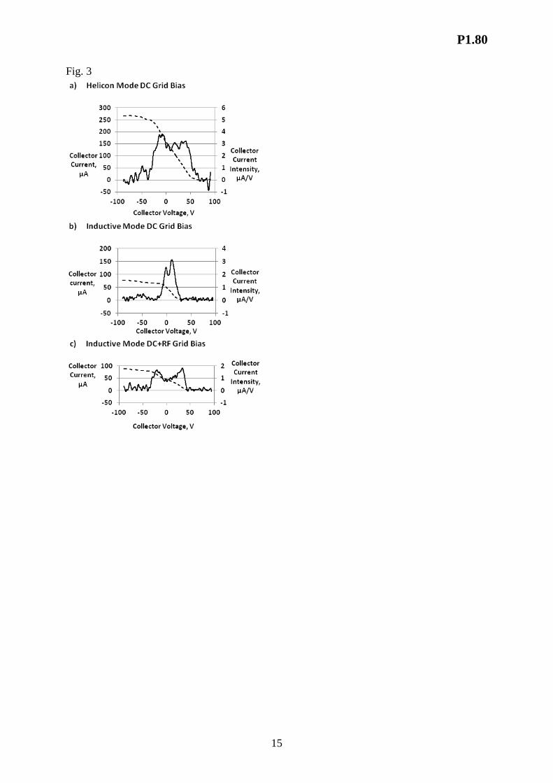
We analyzed the ion energy distribution (IED) by constructing a gridded energy analyzer
in place of the sample. The single grid retarding field energy analyzer (RFEA) is the same
experimental set up used for the study of the electric field in W fuzz growth [18]. To use the
set up to measure the IED we biased the grid with -50 V and swept the voltage on the
collector from -100 V to 100 V while measuring the current to the collector. The space
between the grid and the collector was 380 μm while the ionization mean free path was on the
order of 1 cm. Also, the drift space was low enough to avoid space charge effects. However,
we found that the current to the collector only reached saturation when the collector voltage
was lower than the grid bias, as seen in Fig. 3. The simplicity of the single grid RFEA
requires additional consideration of secondary electron currents. The ion current to the
collector is the same polarity as electron current leaving the collector. The current signal is
saturated below the grid bias because of the secondary electron emission leaving the analyzer
P1.80
5
and being lost to the plasma. When the collector voltage sweeps above the grid bias, the
secondary electrons are suppressed back to the collector. A second level of saturation is
observed in this voltage region where the secondary electrons are contained and the collector
voltage is still below the lowest energy ions. The derivative of the measured current-voltage
characteristic is proportional to the local IED in the plasma that passes through the sheath and
the biased grid. Since the collector voltage sweep rate is much slower than the fluctuations in
the plasma or sheath, the derivative of the current-voltage characteristic represents the time-
averaged IED incident on the sample at the center of the plasma. As can be seen in Fig. 3a,
the IED at the center of the helicon mode is a broad, bimodal distribution with a FWHM of
approximately 78 eV and a value of 47 eV between the two dominant peaks in the
distribution. The energy resolution of the single grid RFEA is estimated to be 5 eV.
The time-averaged IED in helicon sources can be broadened due to the RF modulation of
the plasma potential [19]. To investigate if RF broadening or time modulation of the plasma
potential could be affecting the resulting surface morphology in the helicon mode, we tested
the effect of an RF bias on the sample in an inductive mode, which has less RF pickup from
the antenna [20]. The IED measured from the inductive mode is shown in Fig. 3b. There is
little broadening present in the IED. Subjecting a sample with a DC bias of -50 V to the
inductive mode resulted in W fuzz growth, shown in Fig. 4. To impose RF broadening in the
time-averaged IED incident on the sample similar to the helicon mode exposure, we
constructed a bias tee circuit so that an RF voltage could be supplied to modulate the DC bias
to the grid, shown schematically in Fig. 1. The input power from the RF bias supply was
selected so that the peak-to-peak value of the sample bias was comparable to the peak-to-peak
value of the bimodal IED from the helicon mode, approximately 50 V peak-to-peak. This
required only 1-2 W of RF power. The voltage waveform was monitored with a high
frequency voltage probe on the bias feedthrough into the plasma chamber. The resulting IED

P1.80
6
measured through the grid with the RF modulated bias in the inductive mode, shown in Fig.
3c, is bimodal with similar characteristics as the IED measured from the center of the helicon
mode. The RF modulated bias was applied to the samples exposed to the inductive mode
plasma to induce NTB growth instead of W fuzz growth.
3. Results and Discussion
3.1. Ion energy modulation effects
Upon applying the RF modulated bias to a W sample with the surface temperature of 1020
K and exposing the sample to the same amount of total collected charge as the helicon mode
sample, or the equivalent of a spatially-averaged He fluence of 5.8 x 1025
m-2
, the sample
remained macroscopically reflective, except for near the edges of the sample and near the
mounting clips. The surface morphology of the outer radii of the sample and under the clip
hardware was W fuzz.
Microscopic inspection revealed NTB growth in the reflective area, as seen in Fig. 5d, but
the NTBs were smaller than those grown in the helicon mode exposure. Also some grains
contained a spread of single nano-tendrils growing 2 μm perpendicular to the surface, shown
in Fig. 5e and 5f. The RF modulation of the ion energy is integral to the transition from W
fuzz to NTB growth in our device, but the difference in size between the NTBs from the
plasma born RF modulation and the sample bias RF modulation could be due to the difference
in flux density in the two exposures. The inductive mode has a flux density one third that of
the helicon mode. The growth of W fuzz has been shown to have a flux density dependence,
but saturates after a certain flux density level is reached [21] that could also be dependent on
the ion energy and surface temperature. In the present case, the NTB width and height from
the surface also increases with increased flux density.
As for the areas of the surface that formed W fuzz in the inductive mode, along the outer
edge of the sample and near the clip hardware, these areas of the sample experience lower

P1.80
7
flux density. The ion flux density radial profile shown in Fig. 2 was measured 10 mm from
the sample axial location. It is unknown how the clip hardware exactly affects the ion flux
density incident on the sample at these locations, but the clips are 3 mm proud of the
surrounding sample surface and could pose a shadowing issue for the sample at larger radii,
which has been shown to diminish the flux density in others’ simulations [22]. The flux
density could be decreased by an order of magnitude, and assuming that the electron
temperature is unchanged, this means that the electron density is decreased, as well. The
lower plasma density means that the sheath thickness increases in these areas, with the final
effect of rectifying the time-modulation we imposed. The IED incident on the sample surfaces
at larger radii is most likely narrow, similar to the IED shown in Fig. 3b.
3.2. Nano-Tendril Bundle Cross Section
The NTB structure was analyzed in more detail by milling with a focused-ion beam in the
SEM. To protect the fine structure of the NTB, a layer of platinum was deposited over the
NTB prior to milling. The NTB after milling is shown in Fig. 6a. A close up of the base of the
NTB is shown in Fig. 6b. We have called these nano-tendril bundles due to this structure. The
nano-tendrils that make up the NTB are very similar in size to the nano-tendrils found in W
fuzz. The porosity of the NTB is estimated to be 0.85 from analysis of the image, which is
similar to the porosity of W fuzz [23–25].
From the cross section, it is revealed that the interface of the NTB and the bulk is almost
level with the surface of the surrounding area, relative to the height of the NTB. However,
viewing more closely, in Fig. 6b, one can see that the surface level is lower than the bulk
material just below the NTB by 150 nm. Put another way, the NTB seems to be situated atop
a pedestal of solid W. The lack of a network of voids below the surface level line and the
presence of the solid pedestal indicate that the W that composes the NTB did not come from

P1.80
8
bulk diffusion from directly beneath the NTB. The W that formed the NTB must have come
from the surrounding area.
4. Conclusions
RF broadened ion energy distribution and/or ion energy modulation was shown to affect
the resulting surface morphology when He plasma is incident on W at 1020 K. W fuzz was
suppressed, but nano-tendrils were still present. Nano-tendril bundles, essentially islands of
nano-tendrils with low coverage (<10%), are observed instead of W fuzz. Through structural
evidence, nano-tendril bundles and single nano-tendrils apparently grow by diffusion of W
from the surface during RF He plasma exposure. These new forms of nano-tendril surface
morphologies provide additional clues in the study of W fuzz growth mechanisms and warrant
further investigation.
5. Acknowledgements
This work is supported by US DOE award DE-SC00-02060. This work made use of the
MRSEC Shared Experimental Facilities at MIT, supported by the National Science
Foundation under award number DMR-08-19762.
6. References
[1] G.M. Wright, D. Brunner, M.J. Baldwin, R.P. Doerner, B. Labombard, B. Lipschultz,
J.L. Terry, D.G. Whyte, Nucl. Fusion 52 (2012) 042003.
[2] S. Takamura, T. Miyamoto, N. Ohno, Nucl. Fusion 52 (2012) 123001.
[3] S. Kajita, S. Takamura, N. Ohno, D. Nishijima, H. Iwakiri, N. Yoshida, Nucl. Fusion
47 (2007) 1358–1366.
[4] A. Lasa, S.K. Tähtinen, K. Nordlund, EPL (Europhysics Lett. 105 (2014) 25002.
[5] S. Takamura, Y. Uesugi, Appl. Surf. Sci. 356 (2015) 888–897.
[6] A.M. Ito, A. Takayama, Y. Oda, T. Tamura, R. Kobayashi, T. Hattori, S. Ogata, N.
Ohno, S. Kajita, M. Yajima, Y. Noiri, Y. Yoshimoto, S. Saito, S. Takamura, H.
P1.80
9
Nakamura, 440 (2014) 134301.
[7] Y. V. Martynenko, M.Y. Nagel, Plasma-Surface Interact. 38 (2012) 996–999.
[8] D. Trufanov, E. Marenkov, S. Krasheninnikov, Phys. Procedia 71 (2015) 20–24.
[9] S.I. Krasheninnikov, Phys. Scr. T145 (2011) 014040.
[10] K.B. Woller, D.G. Whyte, G.M. Wright, J. Nucl. Mater. 463 (2015) 289–293.
[11] W.L. Chan, E. Chason, J. Appl. Phys. 101 (2007).
[12] K.B. Woller, D.G. Whyte, G.M. Wright, in:, 2015 IEEE 26th Symp. Fusion Eng.,
IEEE, Austin, Texas, 2015, pp. 1–6.
[13] R. Ochoukov, D.G. Whyte, D. Brunner, I. Cziegler, B. LaBombard, B. Lipschultz, J.
Myra, J. Terry, S. Wukitch, J. Nucl. Mater. 438 (2013) S875–S878.
[14] C. Charles, A. W. Degeling, T.E. Sheridan, J.H. Harris, M. A. Lieberman, R.W.
Boswell, Phys. Plasmas 7 (2000) 5232.
[15] T. Panagopoulos, D.J. Economou, J. Appl. Phys. 85 (1999) 3435.
[16] G.M. Wright, H.S. Barnard, L.A. Kesler, E.E. Peterson, P.W. Stahle, R.M. Sullivan,
D.G. Whyte, K.B. Woller, Rev. Sci. Instrum. 85 (2014) 023503.
[17] F.F. Chen, Plasma Sources Sci. Technol. 24 (2015) 014001.
[18] K.B. Woller, D.G. Whyte, G.M. Wright, D. Brunner, Submitted to J. Nucl. Mater.
(2016).
[19] J.-H. Kim, H.-Y. Chang, Phys. Plasmas 3 (1996) 1462.
[20] A. Perry, G. Conway, R. Boswell, H. Persing, Phys. Plasmas 9 (2002) 3171.
[21] M.J. Baldwin, R.P. Doerner, D. Nishijima, K. Tokunaga, Y. Ueda, J. Nucl. Mater. 390-
391 (2009) 886–890.
[22] G. Kawamura, N. Ohno, S. Takamura, Y. Tomita, this issue (2016).
[23] M.J. Baldwin, R.P. Doerner, J. Nucl. Mater. 404 (2010) 165–173.
[24] D. Nishijima, M.J. Baldwin, R.P. Doerner, J.H. Yu, J. Nucl. Mater. 415 (2011) S96–

P1.80
10
S99.
[25] S. Kajita, N. Yoshida, R. Yoshihara, N. Ohno, T. Yokochi, M. Tokitani, S. Takamura,
J. Nucl. Mater. 421 (2012) 22–27.

P1.80
11
Figure captions:
Fig. 1. Schematic of the plasma exposure chamber of the DIONISOS experiment. The DC/RF
biasing circuit allows for either DC or RF modulated bias that is monitored with a high
frequency probe at the bias feedthrough into the chamber.
Fig. 2. a) He ion flux density and b) electron temperature radial profiles for the helicon mode
(x) and the inductively-couple mode (□). Measured with a double Langmuir probe located 10
mm axially away from the sample surface location.
Fig. 3. a) Current-voltage characteristic (dashed line) measured on axis in the helicon mode.
The grid had a DC bias of -50 V. The derivative of the characteristic with respect to collector
voltage is proportional to the time-average ion energy distribution passing through the grid
and is shown as the current intensity (solid line). The peak around -50 V in the derivative is
due to secondary electron current being lost from the analyzer. b) Current-voltage
characteristic (dashed line) measured in an inductively-coupled mode with a -50 V DC bias to
the grid. The current intensity is shown as the solid line. c) Current-voltage characteristic
(dashed line) measured in an inductively-coupled mode with a -50 V DC bias modulated at
13.56 MHz with +/- 25 V. The current intensity is shown as the solid line.
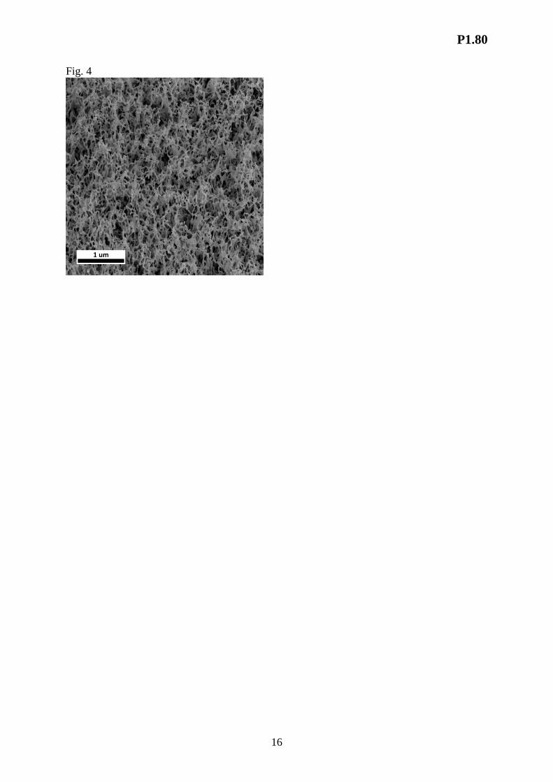
Fig. 4. Scanning electron micrograph of W fuzz grown on a sample at 1020 K in the inductive
mode plasma with a DC bias of -50 V for a He fluence of 5.8 x 1025
m-2
. The local ion energy
distribution is shown in Fig. 3b. The thickness of the W fuzz layer was measured to be 1.5
μm. The viewing angle is 52° from the sample normal.
Fig. 5. a) Scanning electron micrograph showing Nano-Tendril Bundle (NTB) growth on a W
sample after exposure at 1020 K in the helicon mode plasma with a DC bias of -50 V for a
total He fluence of 5.8 x 1025
m-2
. The local He ion flux density of the area in view was 2.5 x
1022
m-2
s-1
. The local ion energy distribution under these conditions is bimodal as shown in
Fig. 3a. b) Micrograph of a NTB from the same sample as shown in a). c) Micrograph near
P1.80
12
the center of a sample exposed with the RF modulated bias in the inductive mode plasma for
the same amount of accumulated charge as the sample in a). d) Detail of the NTB growth in
box labelled B in c). e) Detail of the grain in the box labelled A in c) showing multiple
distinct nano-tendrils growing on the grain. f) Detail of a single nano-tendril from the grain in
d). All viewing angles are 52° from the sample normal.
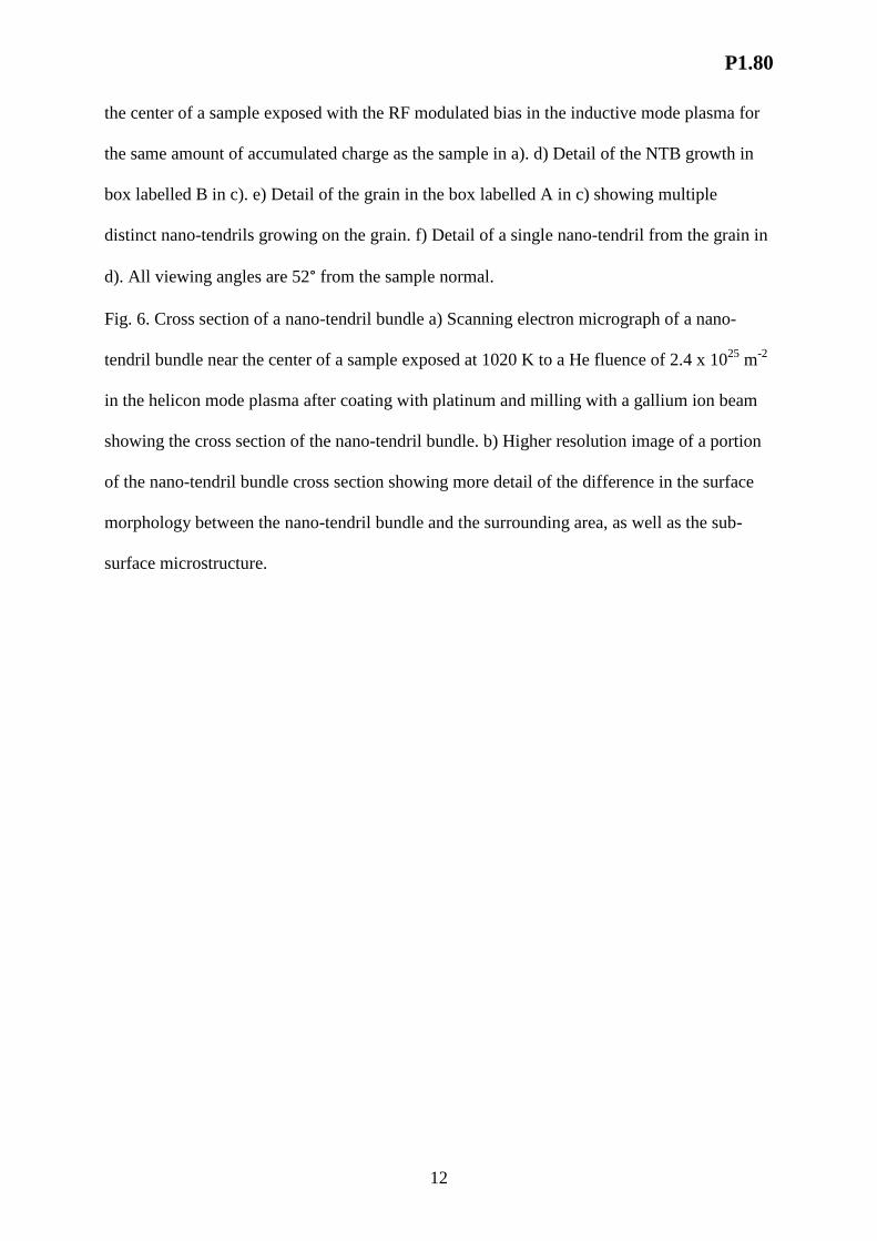
Fig. 6. Cross section of a nano-tendril bundle a) Scanning electron micrograph of a nano-
tendril bundle near the center of a sample exposed at 1020 K to a He fluence of 2.4 x 1025
m-2
in the helicon mode plasma after coating with platinum and milling with a gallium ion beam
showing the cross section of the nano-tendril bundle. b) Higher resolution image of a portion
of the nano-tendril bundle cross section showing more detail of the difference in the surface
morphology between the nano-tendril bundle and the surrounding area, as well as the sub-
surface microstructure.

P1.80
13
Fig. 1

P1.80
14
Fig. 2
P1.80
15
Fig. 3
P1.80
16
Fig. 4

P1.80
17
Fig. 5

P1.80
18
Fig. 6


![Tendril STS 2088 [3T MRI] [OUS] [v1] - SJM/media/manuals/product-manual-pdfs/4/9/… · Certain Tendril STS Model 2088TC lead lengths have been tested for use in the MRI environment](https://img.dokumen.tips/doc/110x75/5f0bea217e708231d432d7bf/tendril-sts-2088-3t-mri-ous-v1-sjm-mediamanualsproduct-manual-pdfs49.jpg)
![Tendril STS 2088 [OUS] - SJM€¦ · Tendril™ STS . Model 2088TC . Active-fixation Bipolar . Steroid-eluting . Endocardial . Pacing leads . User's Manual](https://img.dokumen.tips/doc/110x75/5f01af377e708231d4008cc7/tendril-sts-2088-ous-sjm-tendrila-sts-model-2088tc-active-fixation-bipolar.jpg)


