Embed Size (px)
Citation preview
Systemyde International Corporation ISO7816 Product Specification, 09/03/2015
1
ISO7816 UARTProduct Specification

Systemyde International Corporation ISO7816 Product Specification, 09/03/2015
2
Disclaimer
Systemyde International Corporation reserves the right to make changes at any time, without notice, toimprove design or performance and provide the best product possible. Systemyde International Corporationmakes no warrant for the use of its products and assumes no responsibility for any errors which may appearin this document nor does it make any commitment to update the information contained herein.
Systemyde International Corporation products are not authorized for use in life support devices or systems.Nothing contained herein shall be construed as a recommendation to use any product in violation of existingpatents, copyrights or other rights of third parties. No license is granted by implication or otherwise underany patent, patent rights or other rights, of Systemyde International Corporation. All trademarks are trade-marks of their respective companies.
Every effort has been made to ensure the accuracy of the information contain herein. If you find errors orinconsistencies please bring them to our attention. In all cases, however, the Verilog HDL source code forthe iso7816 design defines “proper operation”.
Copyright © 2014, Systemyde International Corporation. All rights reserved.

Systemyde International Corporation ISO7816 Product Specification, 09/03/2015
3
Table of Contents
Overview -------------------------------------------------------------------------------------------------------5General Features ---------------------------------------------------------------------------------------5ISO7816/EVM4.3 Features --------------------------------------------------------------------------- 5
Signal Descriptions ------------------------------------------------------------------------------------------- 7Card Interface Group ----------------------------------------------------------------------------------7Host Interface Group ----------------------------------------------------------------------------------9Miscellaneous Group ----------------------------------------------------------------------------------10
External Timing -----------------------------------------------------------------------------------------------11Host Interface Timing ----------------------------------------------------------------------------------11Card Interface Timing ----------------------------------------------------------------------------------12
Programming Interface -------------------------------------------------------------------------------------- 17Registers --------------------------------------------------------------------------------------------------17Register Descriptions ----------------------------------------------------------------------------------- 18
Master Control Register --------------------------------------------------------------------------18Direct Control/Status Register ------------------------------------------------------------------19Clock Divisor Register --------------------------------------------------------------------------- 19Clock Control Register --------------------------------------------------------------------------- 20ETU Width Register ------------------------------------------------------------------------------ 20ETU Divider Register ----------------------------------------------------------------------------20Hardware Control Register --------------------------------------------------------------------21Parity Error Limit Register --------------------------------------------------------------------21Time Constant 0 Registers -----------------------------------------------------------------------21Guard Time Register ------------------------------------------------------------------------------ 22Time Constant 1 Registers -----------------------------------------------------------------------22Time Control Register ----------------------------------------------------------------------------22Master Mode Register ----------------------------------------------------------------------------23Power Control Register --------------------------------------------------------------------------- 23Protocol State Register --------------------------------------------------------------------------- 23UART Status Register ----------------------------------------------------------------------------24Protocol Interrupt Enable -----------------------------------------------------------------------25UART Interrupt Enable --------------------------------------------------------------------------25UART Buffer Register ----------------------------------------------------------------------------26
Protocol Constants -------------------------------------------------------------------------------------- 27Verilog Top Level -------------------------------------------------------------------------------------- 28

Systemyde International Corporation ISO7816 Product Specification, 09/03/2015
4
This page intentionally left blank.

Systemyde International Corporation ISO7816 Product Specification, 09/03/2015
5
Overview
The ISO7816 UART contains all of the digital logic necessary to communicate with anISO/IEC 7816 or EMV 4.3 integrated circuit card. The design separates the control regis-ters and bus interface from the core logic, which allows you to redefine the register inter-face to meet your specific requirements.
General Features:
- Technology-independent Verilog HDL implementation.
- 8-bit APB host interface.
- 8-byte receive buffer.
- 8-bit divider for generating card CLK signal from APB clock.
- Flexible multi-mode timers to handle the various ISO7816 time limits.
- Sampling of card serial data consistent with ISO7816 specification.
ISO7816/EMV4.3 Features:
- Protocol state machine to reduce CPU overhead. Time limits set by compile option.
- Automatic initial character TS recognition.
- T=0 and T=1 protocols. T=0 protocol includes automatic retry (programmable limit).
- Dedicated CWT timer.
- Dedicated BWT timer.
Systemyde International Corporation ISO7816 Product Specification, 09/03/2015
6
This page intentionally left blank.
Systemyde International Corporation ISO7816 Product Specification, 09/03/2015
7
Signal Descriptions
The ISO7816 UART sits between a host and an integrated circuit card, and translatesbetween the parallel 8-bit bus of the host and the bidirectional serial signals of the card.None of the ISO7816 UART signals are bidirectional, but will require external (to theUART) 3-state buffers to create true bidirectional signals.
The native host interface is eight bits wide, but it is easy to convert this interface to usesixteen or even thirty-two bits.
The ISO7816 UART is configured and controlled via a set of registers, but in many casesthese registers can be replaced by hard-wired values if necessary to reduce gate count.
Card Interface group:
C_CLK (output, active-High). The Card Clock signal is derived from the PeripheralClock. Initially the Card Clock should be 1MHz, but can be increased undersoftware control if supported by the card.
C_C4IN (input). The Card C4 signal is undefined in ISO7816, but may be used by non-standard cards as an input, output or bidirectional signal. This is the inputfrom pin C4.
C_C4OUT (output). The Card C4 signal is undefined in ISO7816, but may be used bynon-standard cards as an input, output or bidirectional signal. This is the out-put for pin C4.
C_C6IN (input). The Card C6 signal is undefined in ISO7816, but may be used by non-standard cards as an input, output or bidirectional signal. This is the inputfrom pin C6.
C_C6OUT (output). The Card C6 signal is undefined in ISO7816, but may be used bynon-standard cards as an input, output or bidirectional signal. This is the out-put for pin C6.
C_C8IN (input). The Card C8 signal is undefined in ISO7816, but may be used by non-standard cards as an input, output or bidirectional signal. This is the inputfrom pin C8.

Systemyde International Corporation ISO7816 Product Specification, 09/03/2015
8
C_C8OUT (output). The Card C8 signal is undefined in ISO7816, but may be used bynon-standard cards as an input, output or bidirectional signal. This is the out-put for pin C8.
C_DIN (input). The Card Data Input signal is the card I/O signal (C7).
C_DOUT (output). The Card Data Output signal is the serial data output for the card.When the Card Data Output signal is Low, the card I/O signal (C7) should bedriven Low. At all other times the card I/O signal should be pulled High pas-sively. The Card Data Output signal is Low until the card activation sequenceis started and will return Low when the card is deactivated.
C_PRES (input, active High). The Card Present signal should come from a mechanicalcard-present switch. This signal should be High when a card is present andLow when no card is present. If the Card Present signal goes Low the deacti-vation sequence will be automatically initiated.
C_RST (output, active High). The Card Reset signal is the master reset for the card.When the Card Reset signal is Low, the card RST signal (C2) should bedriven Low. The Card Reset signal is Low until the card activation sequenceis started and will return Low when the card is deactivated.
C_VCC18 (output, active High). The Card 1.8V Power Select signal should be used toselect 1.8V for the card power supply.
C_VCC30 (output, active High). The Card 3.0V Power Select signal should be used toselect 3.0V for the card power supply.
C_VCC50 (output, active High). The Card 5.0V Power Select signal should be used toselect 5.0V for the card power supply. The card Power Select outputs areguaranteed to be mutually exclusive. The default selection is 5.0V.
C_VCCOK (input, active High). The Card Power Okay signal should be active when thecard power supply is stable within spec. If the Card Power Okay signal goesLow the deactivation sequence will be automatically initiated.
C_VCCON (output, active High). The Card Power On signal should enable an externalpower supply to power to the card. The Card Power On signal is Low untilthe card activation sequence is started and will return Low when the card isdeactivated.
Systemyde International Corporation ISO7816 Product Specification, 09/03/2015
9
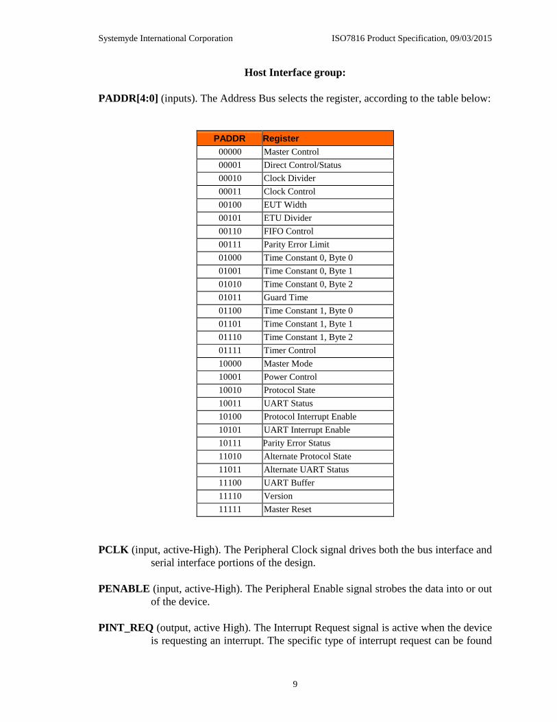
Host Interface group:
PADDR[4:0] (inputs). The Address Bus selects the register, according to the table below:
PADDR Register00000 Master Control00001 Direct Control/Status00010 Clock Divider00011 Clock Control00100 EUT Width00101 ETU Divider00110 FIFO Control00111 Parity Error Limit01000 Time Constant 0, Byte 001001 Time Constant 0, Byte 101010 Time Constant 0, Byte 201011 Guard Time01100 Time Constant 1, Byte 001101 Time Constant 1, Byte 101110 Time Constant 1, Byte 201111 Timer Control10000 Master Mode10001 Power Control10010 Protocol State10011 UART Status10100 Protocol Interrupt Enable10101 UART Interrupt Enable10111 Parity Error Status11010 Alternate Protocol State11011 Alternate UART Status11100 UART Buffer11110 Version11111 Master Reset
PCLK (input, active-High). The Peripheral Clock signal drives both the bus interface andserial interface portions of the design.
PENABLE (input, active-High). The Peripheral Enable signal strobes the data into or outof the device.
PINT_REQ (output, active High). The Interrupt Request signal is active when the deviceis requesting an interrupt. The specific type of interrupt request can be found

Systemyde International Corporation ISO7816 Product Specification, 09/03/2015
10
by reading the Protocol State and UART Status register. This output will bede-asserted when the interrupting condition has been removed.
PRDATA[7:0] (outputs). The Peripheral Read Data Bus is used to transfer data from thedevice to the host. This data bus is normally driven with all zeros, and willonly be valid while both the Peripheral Enable and Peripheral Select signalsare active and the Peripheral Write signal is inactive.
PRESETB (input, active-Low). The Master Reset signal completely initializes thedevice.
PSEL (input, active-High). The Peripheral Select signal enables the device for data trans-fer to or from the host.
PWDATA[7:0] (inputs). The Peripheral Write Data Bus carries write data from the hostto the device. This bus is sampled by the device when the Peripheral Enable,Peripheral Select, and Peripheral Write signals are all active.
PWRITE (input, active-High). The Peripheral Write signal selects the direction for datatransfer between the host and the device. High enables a write from the hostto the device, while Low enables a read from the device by the host.
Miscellaneous group:
ETU_PLS (output, active High). The Elementary Time Unit Pulse signal is a one PCLKwide pulse that signals the serial bit rate. This signal is used by the transmitterto output transmit bits, but can also be used if additional ETU timers arenecessary external to the UART. This signal is output continuously as long asC_RST is High, even if the Card Clock is stopped.
TEST_EN (input, active High). The Test Enable signal overrides the built-in timeconstants for the C_RST Low time to reduce the time required for simulationand test. Enabling test mode masks the upper eight bits of both theRST_EXIT_DLY and WARM_EXIT_DLY time constants, so that only thelower eight bits of these time constants are used. Enabling test mode alsomodifies Timer 0 and Timer 1 so that the increment starts at bit 8, rather thanat bit 0.

Systemyde International Corporation ISO7816 Product Specification, 09/03/2015
11
External Timing
The ISO7816 UART uses the PCLK signal for all timing. As shown in the figure below,all card outputs change relative to the rising edge of the PCLK signal and all card inputsare sampled by the rising edge of the PCLK signal. This figure shows the default casewhen the C_CLK signal is the PCLK signal divided by two. If the C_CLK signal is notactive, the card outputs can change on any PCLK rising edge.
PCLK
Card outputs
Card inputs Valid
C_CLK
Host Interface Timing
Read and write transactions are shown in the figure below. Back-to-back transactions, ofeither type, are allowed.
PCLK
PADDR
PRDATA
PWDATA
PSEL
PWRITE
T1 T2
Valid
PENABLE
T1
Valid
Valid
T2
Valid
Systemyde International Corporation ISO7816 Product Specification, 09/03/2015
12
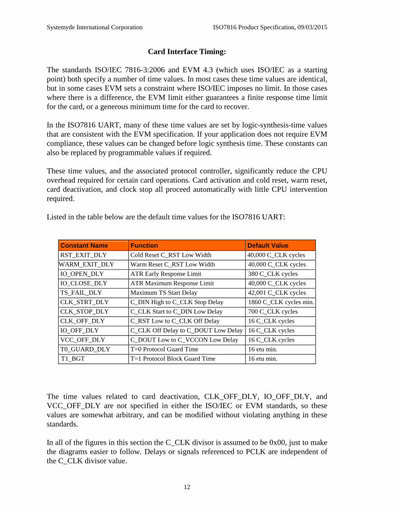
Card Interface Timing:
The standards ISO/IEC 7816-3:2006 and EVM 4.3 (which uses ISO/IEC as a startingpoint) both specify a number of time values. In most cases these time values are identical,but in some cases EVM sets a constraint where ISO/IEC imposes no limit. In those caseswhere there is a difference, the EVM limit either guarantees a finite response time limitfor the card, or a generous minimum time for the card to recover.
In the ISO7816 UART, many of these time values are set by logic-synthesis-time valuesthat are consistent with the EVM specification. If your application does not require EVMcompliance, these values can be changed before logic synthesis time. These constants canalso be replaced by programmable values if required.
These time values, and the associated protocol controller, significantly reduce the CPUoverhead required for certain card operations. Card activation and cold reset, warm reset,card deactivation, and clock stop all proceed automatically with little CPU interventionrequired.
Listed in the table below are the default time values for the ISO7816 UART:
Constant Name Function Default ValueRST_EXIT_DLY Cold Reset C_RST Low Width 40,000 C_CLK cycles
WARM_EXIT_DLY Warm Reset C_RST Low Width 40,000 C_CLK cyclesIO_OPEN_DLY ATR Early Response Limit 380 C_CLK cyclesIO_CLOSE_DLY ATR Maximum Response Limit 40,000 C_CLK cyclesTS_FAIL_DLY Maximum TS Start Delay 42,001 C_CLK cyclesCLK_STRT_DLY C_DIN High to C_CLK Stop Delay 1860 C_CLK cycles min.CLK_STOP_DLY C_CLK Start to C_DIN Low Delay 700 C_CLK cyclesCLK_OFF_DLY C_RST Low to C_CLK Off Delay 16 C_CLK cyclesIO_OFF_DLY C_CLK Off Delay to C_DOUT Low Delay 16 C_CLK cyclesVCC_OFF_DLY C_DOUT Low to C_VCCON Low Delay 16 C_CLK cyclesT0_GUARD_DLY T=0 Protocol Guard Time 16 etu min.T1_BGT T=1 Protocol Block Guard Time 16 etu min.
The time values related to card deactivation, CLK_OFF_DLY, IO_OFF_DLY, andVCC_OFF_DLY are not specified in either the ISO/IEC or EVM standards, so thesevalues are somewhat arbitrary, and can be modified without violating anything in thesestandards.
In all of the figures in this section the C_CLK divisor is assumed to be 0x00, just to makethe diagrams easier to follow. Delays or signals referenced to PCLK are independent ofthe C_CLK divisor value.

Systemyde International Corporation ISO7816 Product Specification, 09/03/2015
13
The figure below shows the timing for card start-up in response to the V_VCCOK signalbecoming active. The rising edge of the C_VCCOK signal is synchronized with PCLKand then initializes the internal C_CLK divider, so that this startup timing is independentof the C_CLK divisor value.
PCLK
C_CxOUT
C_DOUT
C_CLK
C_RST
C_VCCOK
RST_EXIT_DLY
The figure below shows the timing of the C_VCCON signal relative to the bus write thatstarts the card activation sequence. This write initializes the internal C_CLK divider, forconsistent timing.
There is no constraint on the amount of time between the C_VCCON signal going activeand the C_VCCOK signal becoming active, because this time is a function of the powersupply for the card. Software is responsible for setting a time limit while waiting for thecard activation to complete.
PCLK
Bus Write transaction
C_VCCON

Systemyde International Corporation ISO7816 Product Specification, 09/03/2015
14
The figure below shows the timing for the Answer-To-Reset (ATR) sequence, whichoccurs at the end of either a Cold Reset or a Warm Reset. If the character TS starts duringthe IO_OPEN_DLY time, it will be reported as an early answer, and the receiver will notrecognize the start of this character until this delay has expired. A normal response,consisting of both character TS and character T0, should be received before theIO_CLOSE_DLY time has passed. If the character TS has not started before theTS_FAIL_DLY time has passed, the deactivation sequence will be automatically started.
C_CLK
C_DIN
C_DOUT
C_RST
IO_OPEN_DLY
IO_CLOSE_DLY
TS_FAIL_DLY
The figure below shows the timing for the deactivation sequence. As mentionedpreviously, these three delay times are not specified in either the ISO/IEC or EVMspecification.
virtual C_CLK
C_CLK
C_DIN
C_DOUT
C_RST
C_VCCON
CLK_OFF_DLY
IO_OFF_DLY
VCC_OFF_DLY

Systemyde International Corporation ISO7816 Product Specification, 09/03/2015
15
The figure below shows the timing for the Warm Reset sequence. The protocol statemachine will not start a Warm Reset sequence until the reception of the character T0(error-free) is complete.
PCLK
C_DOUT
C_RST
C_VCCOK
WARM_EXIT_DLY
The figure below shows the timing of the C_RST signal relative to the write that starts theWarm Reset sequence. This figure shows the earliest possible activation of the C_RSTsignal. The exact delay depends on the C_CLK divisor, because the C_RST signal issynchronized to a rising edge on the C_CLK signal.
PCLK
bus Write transaction
C_RST
The figure below shows the timing for stopping the clock. In addition to the timingrequirement relative to the C_DIN signal, the protocol state machine does not allow theclock to stop at any time while a character is being received or transmitted. This allowsthe Clock Control Register to be written during the final character transfer before theclock is to be stopped. The C_CLK signal can be stopped in either state, under programcontrol.
C_CLK
C_CLK
C_DIN
CLK_STOP_DLY CLK_STRT_DLY

Systemyde International Corporation ISO7816 Product Specification, 09/03/2015
16
This page intentionally left blank.

Systemyde International Corporation ISO7816 Product Specification, 09/03/2015
17
Programming Interface
Registers
Register Name Mnemonic I/O address R/W ResetMaster Control Register MCR 0x00 R/W 00000000Direct Control/Status Register DCSR 0x01 R/W 00000000Clock Divisor Register CDR 0x02 R/W 00000000Clock Control Register CCR 0x03 R/W 00000000ETU Width Register EWR 0x04 R/W 00000000ETU Divider Register EDR 0x05 R/W 00001100FIFO Control Register FCR 0x06 R/W 00000000Parity Error Limit Register PELR 0x07 R/W 01110111Time Constant 0, Byte 0 Register TC00R 0x08 R/W 01011111Time Constant 0, Byte 1 Register TC01R 0x09 R/W 00100111Time Constant 0, Byte 2 Register TC02R 0x0A R/W 00000000Guard Time Register GTR 0x0B R/W 11111111Time Constant 1, Byte 0 Register TC10R 0x0C R/W 11111111Time Constant 1, Byte 1 Register TC11R 0x0D R/W 01001010Time Constant 1, Byte 2 Register TC12R 0x0E R/W 00000000Timer Control Register TCR 0x0F R/W 00000000Master Mode Register MMR 0x10 R/W 00000000Power Control Register PCR 0x11 R/W 00000000Protocol State Register PSR 0x12 R 00000001UART Status Register USR 0x13 R 00000000Protocol Interrupt Enable Register PIER 0x14 R/W 00000000UART Interrupt Enable Register UIER 0x15 R/W 00000000Parity Error Status Register PESR 0x17 R 00000000Alternate Protocol State APSR 0x1A R 00000001Alternate UART Status AUSR 0x1B R 00000000UART Buffer Register UBR 0x1C R&W xxxxxxxxVersion Register VR 0x1E R 00000000Master Reset Register MRR 0x1F R/W 00000001

Systemyde International Corporation ISO7816 Product Specification, 09/03/2015
18
Register Descriptions
Master Control Register (MCR) (Address = 0x00)Bit(s) Value Description
0 Normal UART operation.
71
Bypass operation. In this mode all card interface signals are under directprogram control. For security reasons, bypass operation only works while theprotocol state machine is in the inactive state.
6 This bit is reserved and should always be written with zero.0 Normal operation
51
Deactivate if initial character TS is not 0x3B (direct convention) or 0x3F(inverse convention) or either (automatic convention detection enabled).Deactivate if parity error limit is reached before valid character TS is received.
0 Normal operation4
1 Deativate in case of parity error (receive or transmit). Primarily for use duringAnswer-To-Reset (ATR). Should only be used in protocol T=0.
0 Disable automatic automatic convention detection. In this case the conventionmust be set by software before starting the activation sequence.
31
Enable automatic convention detection during the initial character TS. In thismode the protocol state machine will automatically select the convention and thecharacter TS will not be transferred to the receive buffer. No receive bufferinterrupt will be generated for the character TS.
0Direct convention: Serial data is LSB first and normal polarity. With automaticconvention detection, this bit is set by the hardware based on the contents of theinitial character TS.2
1 Inverse convention: Serial data is MSB first and inverted polarity.Read Warm Start completed.
0Write No effect.Read Warm Start in progress.
11
Write
Setting this bit initiates a Warm Start. This bit is ignored if theprotocol state machine is not in the "active" state. The protocol statemachine automatically does a warm start if there is no Answer-to-Reset.
Read Deactivation process in progress or completed.
0Write
Clearing this bit starts the card deactivation process. Thedeactivation process can be started at any time. If either C_VCCOKor C_PRES go inactive the deactivation process will be initiated.
Read Activation process in progress or completed.
0
1Write Setting this bit initiates the card activation process.

Systemyde International Corporation ISO7816 Product Specification, 09/03/2015
19
Direct Control/Status Register (DCSR) (Address = 0x01)Bit(s) Value Description
7:1 WriteThe state of the various card signals will only be affected if both th C_VCCONand C_VCCOK signals are active. This guarantees that all card signals will beLow during card insertion.
Read Reports the current state of the C_C8IN (C8) pin on the card interface.7
Write Sets the state of the C_C8OUT (C8) pin on the card interface.Read Reports the current state of the C_DIN (C7) pin on the card interface.
Normal No effect.6Write
Bypass Sets the state of the C_DOUT (C7) pin on the card interface.Read Reports the current state of the C_C6IN (C6) pin on the card interface.
5Write Sets the state of the C_C6OUT (C6) pin on the card interface.Read Reports the current state of the C_PRES signal.
4Write No effect.Read Reports the current state of the C_C4IN (C4) pin on the card interface.
3Write Sets the state of the C_C4OUT (C4) pin on the card interface.Read Reports the current state of the C_CLK (C3) pin on the card interface.
Normal No effect.2Write
Bypass Sets the state of the C_CLK (C3) pin on the card interface.Read Reports the current state of the C_RST (C2) pin on the card interface.
Normal No effect.1Write
Bypass Sets the state of the C_RST (C2) pin on the card interface.Read Reports the current state of the C_VCCOK signal..
Normal No effect.0Write
Bypass Sets the state of the C_VCCON pin on the card interface.
Clock Divisor Register (CDR) (Address = 0x02)Bit(s) Value Description
7:0
Time constant for the C_CLK divider. The C_CLK frequency is the PCLKfrequency divided by 2*n. In other words, the C_CLK signal is High for “n” PCLK cycles and Low for “n” PCLK cycles. The time constant should only be changed while the card is inactive or while both the UART and the card are in thereceive state. A time constant of 0x00 operates the same as 0x01. The C_CLKdivider will never generate "runt" output pulses.

Systemyde International Corporation ISO7816 Product Specification, 09/03/2015
20
Clock Control Register (CCR) (Address = 0x03)Bit(s) Value Description
7:2 These bits are ignored when written, and always return zeros when read.
0The C_CLK signal runs continuously, or start the C_CLK signal. Hardwareautomatically enforces the C_CLK start-to-next character delay when starting upthe C_CLK signal.
1
1Stop the C_CLK signal after character transmission or reception. Hardwareautomatically enforces the character-to-C_CLK stop delay. This bit may be setat any time during or after the last character transfer.
0 When stopping the C_CLK signal, stop with the C_CLK signal in the Low state.0
1 When stopping the C_CLK signal, stop with the C_CLK signal in the High state.
ETU Width Register (EWR) (Address = 0x04)Bit(s) Value Description
7:1 These bits are ignored when written, and always return zeros when read.0 ETU is 31 cycles of the ETU divider output. This is the default value.
01 ETU is 32 cycles of the ETU divider output.
ETU Divider Register (EDR) (Address = 0x05)Bit(s) Value Description
7:0Time constant for the ETU generator. This generator counts the C_CLK signalmodulo n. A time constant of 0x00 operates the same as 0x01. The default valueis 0x0C, for an ETU that is 372 (31 x 12) clocks.
Systemyde International Corporation ISO7816 Product Specification, 09/03/2015
21
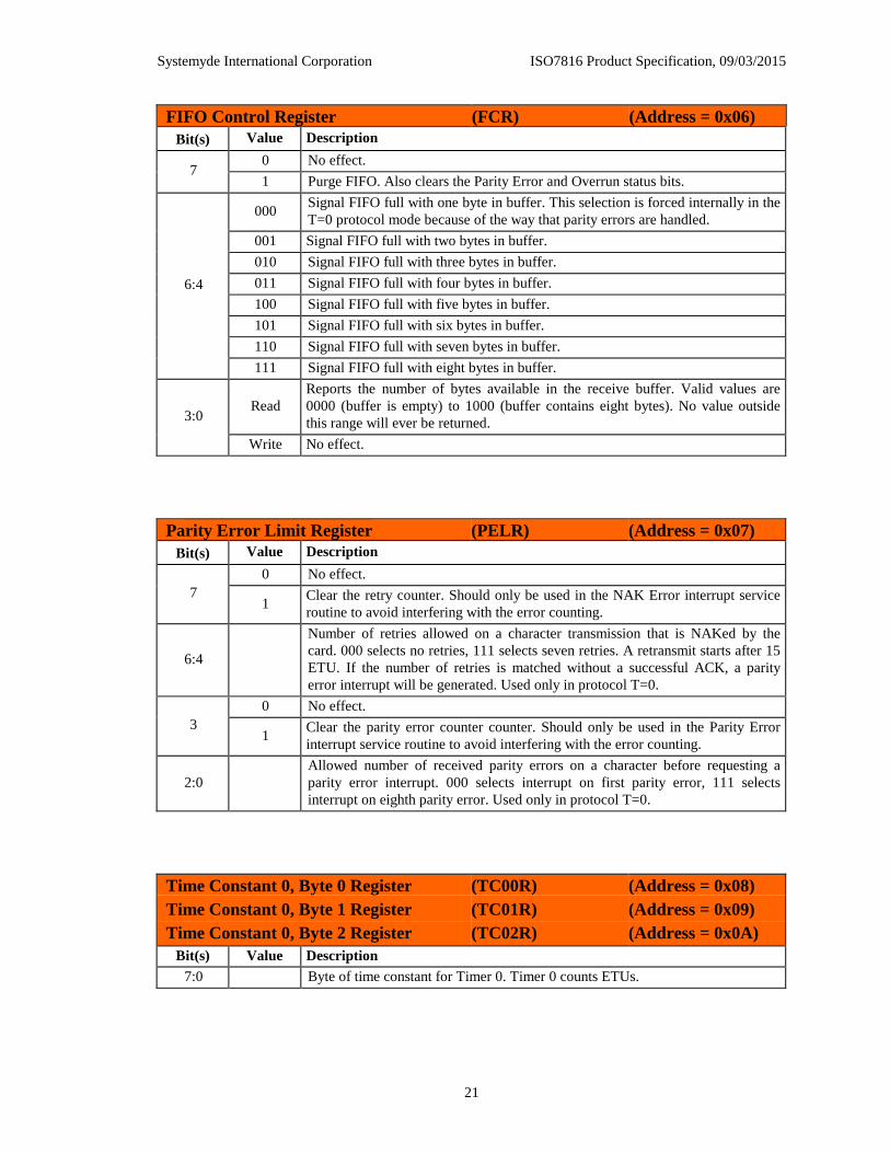
FIFO Control Register (FCR) (Address = 0x06)Bit(s) Value Description
0 No effect.7
1 Purge FIFO. Also clears the Parity Error and Overrun status bits.
000 Signal FIFO full with one byte in buffer. This selection is forced internally in theT=0 protocol mode because of the way that parity errors are handled.
001 Signal FIFO full with two bytes in buffer.010 Signal FIFO full with three bytes in buffer.011 Signal FIFO full with four bytes in buffer.100 Signal FIFO full with five bytes in buffer.101 Signal FIFO full with six bytes in buffer.110 Signal FIFO full with seven bytes in buffer.
6:4
111 Signal FIFO full with eight bytes in buffer.
ReadReports the number of bytes available in the receive buffer. Valid values are0000 (buffer is empty) to 1000 (buffer contains eight bytes). No value outsidethis range will ever be returned.3:0
Write No effect.
Parity Error Limit Register (PELR) (Address = 0x07)Bit(s) Value Description
0 No effect.7
1 Clear the retry counter. Should only be used in the NAK Error interrupt serviceroutine to avoid interfering with the error counting.
6:4
Number of retries allowed on a character transmission that is NAKed by thecard. 000 selects no retries, 111 selects seven retries. A retransmit starts after 15ETU. If the number of retries is matched without a successful ACK, a parityerror interrupt will be generated. Used only in protocol T=0.
0 No effect.3
1 Clear the parity error counter counter. Should only be used in the Parity Errorinterrupt service routine to avoid interfering with the error counting.
2:0Allowed number of received parity errors on a character before requesting aparity error interrupt. 000 selects interrupt on first parity error, 111 selectsinterrupt on eighth parity error. Used only in protocol T=0.
Time Constant 0, Byte 0 Register (TC00R) (Address = 0x08)Time Constant 0, Byte 1 Register (TC01R) (Address = 0x09)Time Constant 0, Byte 2 Register (TC02R) (Address = 0x0A)
Bit(s) Value Description7:0 Byte of time constant for Timer 0. Timer 0 counts ETUs.
Systemyde International Corporation ISO7816 Product Specification, 09/03/2015
22
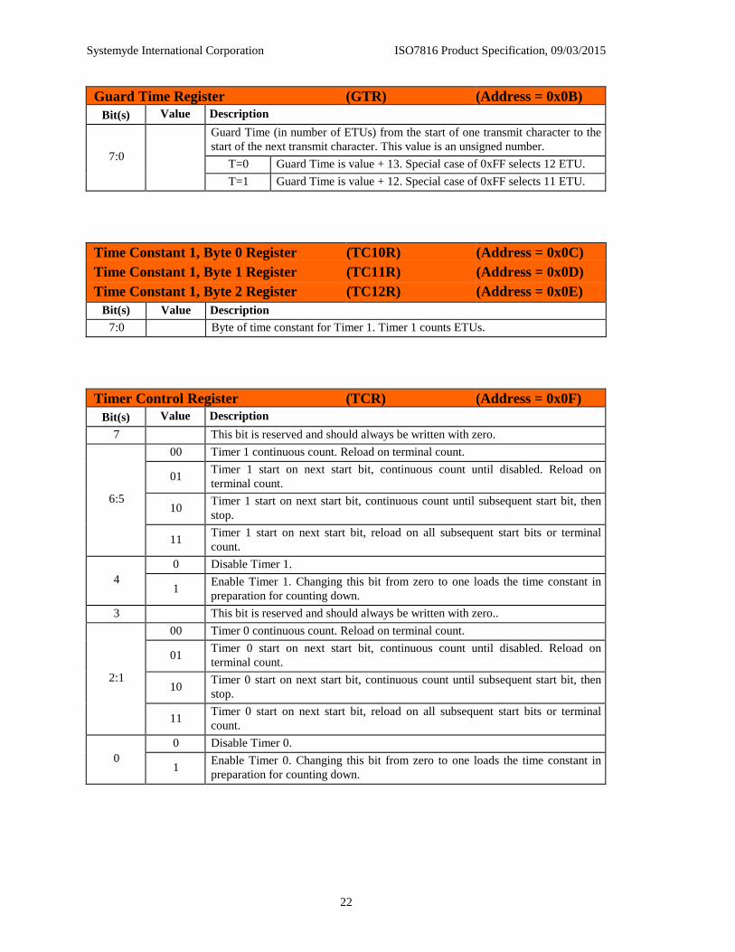
Guard Time Register (GTR) (Address = 0x0B)Bit(s) Value Description
Guard Time (in number of ETUs) from the start of one transmit character to thestart of the next transmit character. This value is an unsigned number.
T=0 Guard Time is value + 13. Special case of 0xFF selects 12 ETU.7:0
T=1 Guard Time is value + 12. Special case of 0xFF selects 11 ETU.
Time Constant 1, Byte 0 Register (TC10R) (Address = 0x0C)Time Constant 1, Byte 1 Register (TC11R) (Address = 0x0D)Time Constant 1, Byte 2 Register (TC12R) (Address = 0x0E)
Bit(s) Value Description7:0 Byte of time constant for Timer 1. Timer 1 counts ETUs.
Timer Control Register (TCR) (Address = 0x0F)Bit(s) Value Description
7 This bit is reserved and should always be written with zero.00 Timer 1 continuous count. Reload on terminal count.
01 Timer 1 start on next start bit, continuous count until disabled. Reload onterminal count.
10 Timer 1 start on next start bit, continuous count until subsequent start bit, thenstop.
6:5
11 Timer 1 start on next start bit, reload on all subsequent start bits or terminalcount.
0 Disable Timer 1.4
1 Enable Timer 1. Changing this bit from zero to one loads the time constant inpreparation for counting down.
3 This bit is reserved and should always be written with zero..00 Timer 0 continuous count. Reload on terminal count.
01 Timer 0 start on next start bit, continuous count until disabled. Reload onterminal count.
10 Timer 0 start on next start bit, continuous count until subsequent start bit, thenstop.
2:1
11 Timer 0 start on next start bit, reload on all subsequent start bits or terminalcount.
0 Disable Timer 0.0
1 Enable Timer 0. Changing this bit from zero to one loads the time constant inpreparation for counting down.

Systemyde International Corporation ISO7816 Product Specification, 09/03/2015
23
Master Mode Register (MMR) (Address = 0x10)Bit(s) Value Description
7:3 These bits are ignored when written, and always return zeros when read.0 Receive Mode.
21
Transmit Mode. Setting this bit to one automatically switches MSR[0] to reportTransmit Buffer Empty status in MSR[0] and will generate in interrupt if enabledin the UIER. This bit can only be set while the UART is in the Active state.
0 Software-controlled Transmit/Receive operation.
11
Automatically enter Receive Mode (and clear MMR[2]) after the next transmitcharacter that is not NAKed. This bit is also automatically cleared after the nexttransmit character. This bit can only be set while the UART is in the Active state.
0 Protocol T=0. Character transfer includes an error-signal response. There is noreceive FIFO in this mode.
01
Protocol T=1. Character transfers do not include an error-signal response. Thisoption should be selected during the ATR character transfers to inhibit any error-signal response.
Power Control Register (PCR) (Address = 0x11)Bit(s) Value Description
7:2 This bits are ignored when written, and always returns zeros when read.00 C_VCC50 output is High, to select 5.0V for card power supply.01 This bit combination is reserved and should not be used.10 C_VCC30 output is High, to select 3.0V for card power supply.
1:0
11 C_VCC18 output is High, to select 1.8V for card power supply.
Protocol State Register (PSR) (Address = 0x12)Alternate Protocol State Register (APSR) (Address = 0x1A)
Bit(s) Value Description
PSR Read operation clears Protocol Interrupt-Pending status.Read
APSR Read operation does not clear Protocol Interrupt-Pending Status.0x80 Active state. Card is active, with characters TS and T0 complete.
0x40 Waiting-For-T0 state. Card is active, and either waiting for or receiving thecharacter T0.
0x20 Waiting-For-TS state. Card is active, and either waiting for or receiving thecharacter TS.
0x10 Activation/Reset state. Card power on and powered. RST is Low.0x08 Waiting-For-Power state. Card power on, waiting for VCCOK.0x04 Deactivation state. Card is being deactivated.
0x02 Activation-Timeout state. Card did not respond with ATR within window,waiting to start deactivation.
7:0
0x01 Power-Off state. Card power is off, and all card signals are Low.
Systemyde International Corporation ISO7816 Product Specification, 09/03/2015
24
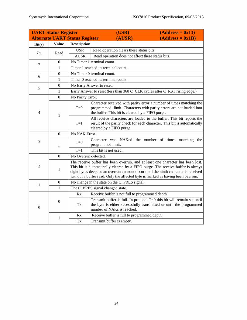
UART Status Register (USR) (Address = 0x13)Alternate UART Status Register (AUSR) (Address = 0x1B)
Bit(s) Value Description
USR Read operation clears these status bits.7:1 Read
AUSR Read operation does not affect these status bits.0 No Timer 1 terminal count.
71 Timer 1 reached its terminal count.0 No Timer 0 terminal count.
61 Timer 0 reached its terminal count.0 No Early Answer to reset.
51 Early Answer to reset (less than 368 C_CLK cycles after C_RST rising edge.)0 No Parity Error.
T=0Character received with parity error a number of times matching theprogrammed limit. Characters with parity errors are not loaded intothe buffer. This bit is cleared by a FIFO purge.4
1
T=1All receive characters are loaded to the buffer. This bit reports theresult of the parity check for each character. This bit is automaticallycleared by a FIFO purge.
0 No NAK Error.
T=0 Character was NAKed the number of times matching theprogrammed limit.
31
T=1 This bit is not used.0 No Overrun detected.
21
The receive buffer has been overrun, and at least one character has been lost.This bit is automatically cleared by a FIFO purge. The receive buffer is alwayseight bytes deep, so an overrun cannout occur until the ninth character is receivedwithout a buffer read. Only the affected byte is marked as having been overrun.
0 No change in the state on the C_PRES signal.1
1 The C_PRES signal changed state.Rx Receive buffer is not full to programmed depth.
0Tx
Transmit buffer is full. In protocol T=0 this bit will remain set untilthe byte is either sucesssfully transmitted or until the programmednumber of NAKs is reached.
Rx Receive buffer is full to programmed depth.
0
1Tx Transmit buffer is empty.

Systemyde International Corporation ISO7816 Product Specification, 09/03/2015
25
Protocol Interrupt Enable Register (UIER) (Address = 0x14)Bit(s) Value Description
0 Disable interrupt on entering Active state.7
1 Enable interrupt on entering Active state.0 Disable interrupt on entering Waiting-For-T0 state.
61 Enable interrupt on entering Waiting-For-T0 state.0 Disable interrupt on entering Waiting-For-TS state.
51 Enable interrupt on entering Waiting-For-TS state.0 Disable interrupt on entering Activation/Reset state.
41 Enable interrupt on entering Activation/Reset state.0 Disable interrupt on entering Waiting-For-Power state.
31 Enable interrupt on entering Waiting-For-Power state.0 Disable interrupt on entering Deactivation state.
21 Enable interrupt on entering Deactivation state.0 Disable interrupt on entering Activation-Timeout state.
11 Enable interrupt on entering Activation-Timeout state.0 Disable interrupt on entering Power-Off state.
01 Enable interrupt on entering Power-Off state.
UART Interrupt Enable Register (PIER) (Address = 0x15)Bit(s) Value Description
0 Disable interrupt on Timer 1 terminal count.7
1 Enable interrupt on Timer 1 terminal count.0 Disable interrupt on Timer 0 terminal count.
61 Enable interrupt on Timer 0 terminal count.0 Disable interrupt on Early Answer To Reset
51 Enable interrupt on Early Answer To Reset0 Disable interrupt on Parity Error.
41 Enable interrupt on Parity Error.0 Disable interrupt on NAK Error.
31 Enable interrupt on NAK Error.0 Disable interrupt on Overrun Error.
21 Enable interrupt on Overrun Error.
0 Disable interrupt on C_PRES signal transition.1
1 Enable interrupt on C_PRES signal transition.0 Disable interrupt on Receive Buffer Full or Transmit Buffer Empty.
01 Enable interrupt on Receive Buffer Full or Transmit Buffer Empty.

Systemyde International Corporation ISO7816 Product Specification, 09/03/2015
26
Parity Error Status Register (PESR) (Address = 0x17)Bit(s) Value Description
7 This bit is ignored when written, and always returns zero when read.
6:4 ReadCurrent number of NAKs received on character being transmitted. Used only inprotocol T=0.
3 This bit is ignored when written, and always returns zero when read.
2:0 ReadCurrent number of received parity errors on character being received. Used onlyin protocol T=0.
UART Buffer Register (UBR) (Address = 0x1C)Bit(s) Value Description
7:0 Read Returns the contents of the Receive Buffer, and removes this character from thebuffer.
Write Loads the Transmit Buffer with a character for transmission. Transmission willstart as soon as allowed by the various time limits (CWT and BWT).
Version Register (VR) (Address = 0x1E)Bit(s) Value Description
7:0 Read Returns an 8-bit version identifier. Currently 0x00, set at compile time.
Master Reset Register (MRR) (Address = 0x1F)Bit(s) Value Description
7:1 These bits are ignored during writes and will always return zeros when read.0 0 Normal operation.
1 Reset all control registers while this bit is set. Bit must be cleared beforeattempting to write to other registers.

Systemyde International Corporation ISO7816 Product Specification, 09/03/2015
27
Protocol Constants
Protocol timer values are set by logic-synthesis-time values that are consistent with theEVM specification. If your application does not require EVM compliance, these valuescan be changed before logic synthesis time. These constants can also be replaced byprogrammable values if required.
Shown below are the constants from the Verilog file used in the design:
`define RST_EXIT_DLY 16'h9c40 /* 40000 RST Low Width */`define RST_EXIT_TST 16'h0040 /* 64 RST Low Width */
`define WARM_EXIT_DLY 16'h9c40 /* 40000 Warm RST Low Width */`define WARM_EXIT_TST 16'h0040 /* 64 Warm RST Low Width */
`define IO_OPEN_DLY 9'h17b /* 380 I/O Min Delay */`define IO_CLOSE_DLY 16'h9c3f /* 40000 I/O Max Delay */`define TS_FAIL_DLY 16'ha410 /* 42001 Max TS Start Delay */
`define CLK_STOP_DLY 11'h743 /* 1860 I/O High to CLK stop */`define CLK_STRT_DLY 11'h2bb /* 700 CLK Start to I/O Low */
`define CLK_OFF_DLY 5'h0f /* 16 RST Off to CLK Off */`define IO_OFF_DLY 5'h0f /* 16 CLK Off to I/O Low */`define VCC_OFF_DLY 5'h0f /* 16 I/O Low to VCC Off */
`define T0_GUARD_DLY 5'h10 /* 16 strt-strt opp dir */`define T1_BGT 5'h16 /* 22 block guard time */
/****************************************************************************************//* default bit rate *//****************************************************************************************/`define DBIT 744 /* 744 PCLK/bit */`define DBITH 372 /* 372 PCLK/half-bit */`define BRATE 31 /* rate integer */`define BDIV 12 /* divide integer */

Systemyde International Corporation ISO7816 Product Specification, 09/03/2015
28
Verilog Top Level
Shown below are the top-level Verilog connections:
module iso7816 (C_C4OUT, C_C6OUT, C_C8OUT, C_CLK, C_DOUT, C_RST, C_VCC18, C_VCC30,C_VCC50, C_VCCON, ETU_PLS, PINT_REQ, PRDATA, C_C4IN, C_C6IN, C_C8IN,C_DIN, C_PRES, C_VCCOK, PADDR, PCLK, PENABLE, PRESETB, PSEL, PWDATA,PWRITE, TEST_EN);
input C_C4IN; /* card C4 connector input */input C_C6IN; /* card C6 connector input */input C_C8IN; /* card C8 connector input */input C_DIN; /* card data input */input C_PRES; /* card present */input C_VCCOK; /* card power okay */input PCLK; /* peripheral bus clock */input PENABLE; /* peripheral enable */input PRESETB; /* master reset */input PSEL; /* peripheral select */input PWRITE; /* peripheral write enable */input TEST_EN; /* test mode enable */input [4:0] PADDR; /* peripheral address bus */input [7:0] PWDATA; /* peripheral write data bus */output C_C4OUT; /* card C4 connector output */output C_C6OUT; /* card C6 connector output */output C_C8OUT; /* card C8 connector output */output C_CLK; /* card clock */output C_DOUT; /* card data output */output C_RST; /* card reset */output C_VCC18; /* card voltage 1.8V select */output C_VCC30; /* card voltage 3.0V select */output C_VCC50; /* card voltage 5.0V select */output C_VCCON; /* card power enable */output ETU_PLS; /* etu timing clock */output PINT_REQ; /* interrupt request */output [7:0] PRDATA; /* peripheral read data bus */


![ARM PrimeCell™ - access.ee.ntu.edu.twaccess.ee.ntu.edu.tw/course/SOC實驗教材/Version 3/Lab05... · PWDATA[7:0] PADDR[11:2] PSEL PENABLE PRDATA[7:0] PCLK PRESETn PWRITE AMBA](https://img.dokumen.tips/doc/110x75/5af40ceb7f8b9a154c8dc61c/arm-primecell-version-3lab05pwdata70-paddr112-psel-penable.jpg)