Embed Size (px)
Citation preview

Section 12. I/O Ports with Peripheral Pin Select (PPS)
I/O Ports
12
This section of the manual contains the following topics:12.1 Introduction ...................................................................................................................... 212.2 I/O Port Control Registers ................................................................................................ 212.3 Peripheral Multiplexing..................................................................................................... 712.4 Peripheral Pin Select........................................................................................................ 912.5 Port Descriptions............................................................................................................ 1912.6 Change Notification (CN) Pins ....................................................................................... 1912.7 Register Maps ................................................................................................................ 2112.8 Related Application Notes.............................................................................................. 2212.9 Revision History ............................................................................................................. 23
© 2007 Microchip Technology Inc. Advance Information DS39711B-page 12-1
Section 12. I/O PortsI/O
Ports
12
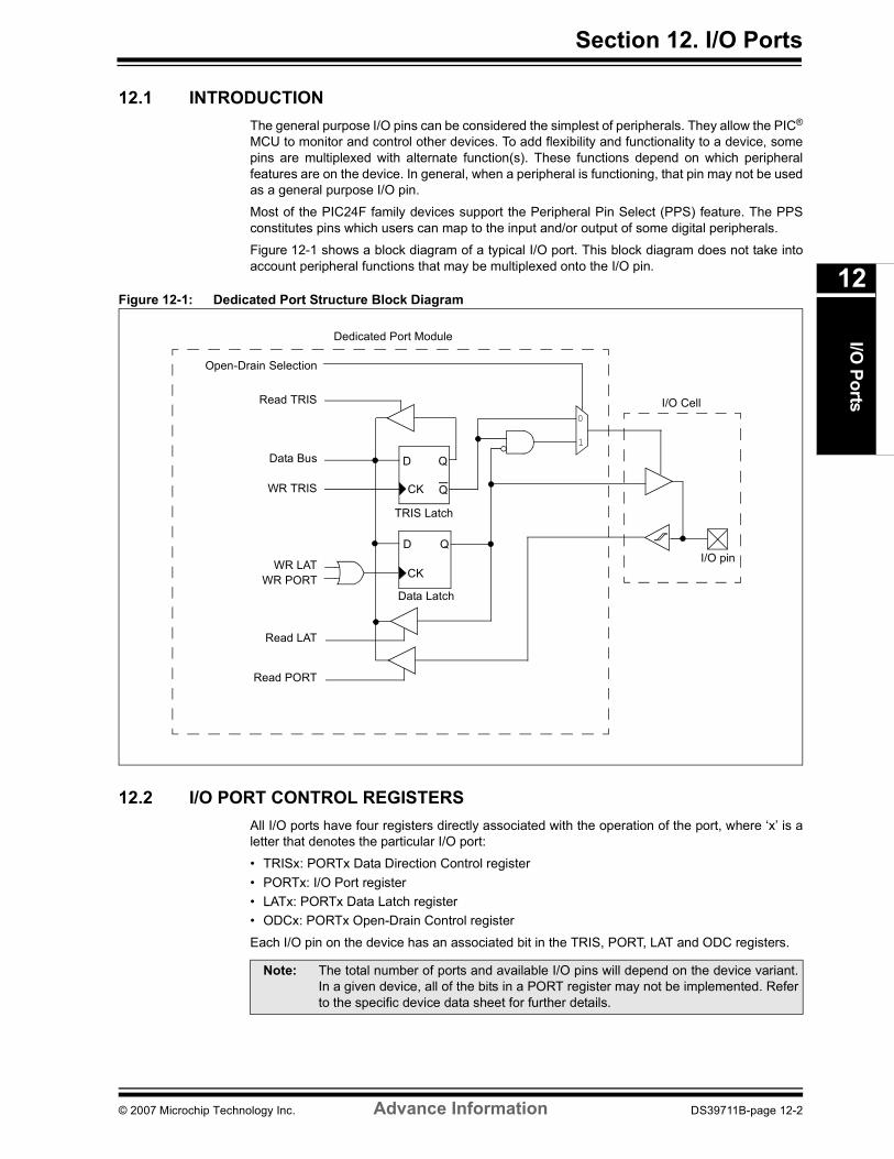
12.1 INTRODUCTIONThe general purpose I/O pins can be considered the simplest of peripherals. They allow the PIC®
MCU to monitor and control other devices. To add flexibility and functionality to a device, somepins are multiplexed with alternate function(s). These functions depend on which peripheralfeatures are on the device. In general, when a peripheral is functioning, that pin may not be usedas a general purpose I/O pin.
Most of the PIC24F family devices support the Peripheral Pin Select (PPS) feature. The PPSconstitutes pins which users can map to the input and/or output of some digital peripherals.
Figure 12-1 shows a block diagram of a typical I/O port. This block diagram does not take intoaccount peripheral functions that may be multiplexed onto the I/O pin.
Figure 12-1: Dedicated Port Structure Block Diagram
12.2 I/O PORT CONTROL REGISTERSAll I/O ports have four registers directly associated with the operation of the port, where �x� is aletter that denotes the particular I/O port:
� TRISx: PORTx Data Direction Control register� PORTx: I/O Port register� LATx: PORTx Data Latch register� ODCx: PORTx Open-Drain Control register
Each I/O pin on the device has an associated bit in the TRIS, PORT, LAT and ODC registers.
QD
CK
WR LAT
TRIS Latch
I/O pin
WR PORT
Data Bus
QD
CK
Data Latch
Read LAT
Read PORT
Read TRIS
WR TRIS
I/O Cell
Dedicated Port Module
0
1
Open-Drain Selection
Q
Note: The total number of ports and available I/O pins will depend on the device variant.In a given device, all of the bits in a PORT register may not be implemented. Referto the specific device data sheet for further details.
© 2007 Microchip Technology Inc. Advance Information DS39711B-page 12-2
PIC24F Family Reference Manual
12.2.1 TRIS RegistersThe TRISx register control bits determine whether each pin associated with the I/O port is aninput or an output. If the TRIS bit for an I/O pin is a �1�, then the pin is an input. If the TRIS bit foran I/O pin is a �0�, then the pin is configured for an output. An easy way to remember this is thata �1� looks like an I (Input) and a �0� looks like an O (Output). All port pins are defined as inputsafter a Reset.
12.2.2 PORT Registers Data on an I/O pin is accessed via a PORTx register. A read of the PORTx register reads thevalue of the I/O pin, while a write to the PORTx register writes the value to the port data latch.This will also be reflected on the PORTx pins if the TRISx is configured as an output and themultiplexed peripherals (if any) are disabled.
Many instructions, such as BSET and BCLR, are read-modify-write operations. Therefore, a writeto a port implies that the port pins are read, the value is modified and then written back to the portdata latch. Care should be taken when read-modify-write instructions are used on the PORTxregisters when some I/O pins associated with the port are configured as inputs. If an I/O pinconfigured as an input is changed to an output, at some later time, an unexpected value may beoutput on the I/O pin. To avoid this, first write to the associated PORTx bit and then change thedirection of the pin as an output.
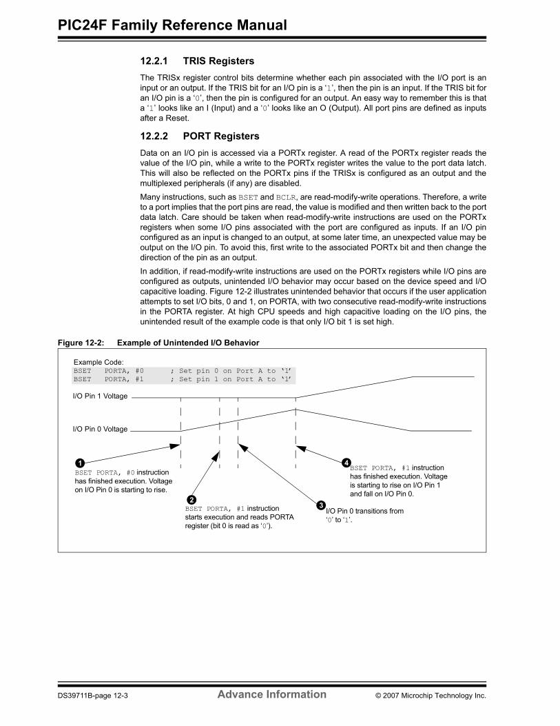
In addition, if read-modify-write instructions are used on the PORTx registers while I/O pins areconfigured as outputs, unintended I/O behavior may occur based on the device speed and I/Ocapacitive loading. Figure 12-2 illustrates unintended behavior that occurs if the user applicationattempts to set I/O bits, 0 and 1, on PORTA, with two consecutive read-modify-write instructionsin the PORTA register. At high CPU speeds and high capacitive loading on the I/O pins, theunintended result of the example code is that only I/O bit 1 is set high.
Figure 12-2: Example of Unintended I/O Behavior
Example Code:BSET PORTA, #0 ; Set pin 0 on Port A to �1�BSET PORTA, #1 ; Set pin 1 on Port A to �1�
I/O Pin 1 Voltage
I/O Pin 0 Voltage
BSET PORTA, #0 instructionhas finished execution. Voltageon I/O Pin 0 is starting to rise.
1
23
4
BSET PORTA, #1 instructionstarts execution and reads PORTAregister (bit 0 is read as �0�).
I/O Pin 0 transitions from �0� to �1�.
BSET PORTA, #1 instructionhas finished execution. Voltageis starting to rise on I/O Pin 1and fall on I/O Pin 0.
DS39711B-page 12-3 Advance Information © 2007 Microchip Technology Inc.

Section 12. I/O PortsI/O
Ports
12
12.2.3 LAT RegistersThe LATx register associated with an I/O pin eliminates the problems that could occur withread-modify-write instructions. A read of the LATx register returns the values held in the portoutput latches instead of the values on the I/O pins. A read-modify-write operation on the LATxregister, associated with an I/O port, avoids the possibility of writing the input pin values into theport latches. A write to the LATx register has the same effect as a write to the PORTx register.
The differences between the PORTx and LATx registers can be summarized as follows:
� A write to the PORTx register writes the data value to the port latch.� A write to the LATx register writes the data value to the port latch.� A read of the PORTx register reads the data value on the I/O pin.� A read of the LATx register reads the data value held in the port latch.
Any bit and its associated data and control registers that are not valid for a particular device willbe disabled. That means the corresponding LATx and TRISx registers, and the port pin, will readas zeros.
12.2.4 ODC RegistersEach I/O pin can be individually configured for either normal digital output or open-drain output.This is controlled by the PORTx Open-Drain Control register, ODCx, associated with each I/Opin. If the ODC bit for an I/O pin is �1�, then the pin acts as an open-drain output. If the ODC bitfor an I/O pin is �0�, then the pin is configured for a normal digital output (ODC bit is valid only foroutput pins). After a Reset, the status of all the bits of the ODCx register is set to �0�.
The open-drain feature allows a load to be connected to a voltage higher/lower than VDD on anydesired digital only pins by using external pull-up resistors. The maximum open-drain voltageallowed is the same as the maximum VIH specification and the minimum is VSS. The ODCx reg-ister setting takes effect in all the I/O modes, allowing the output to behave as an open-drain evenif a peripheral is controlling the pin. Although the user could achieve the same effect by manipu-lating the corresponding LAT and TRIS bits, this procedure will not allow the peripheral to operatein Open-Drain mode (except for the default operation of the I2C� pins). Since I2C pins arealready open-drain pins, the ODCx settings do not affect the I2C pins. Also, the ODCx settingsdo not affect the JTAG output characteristics as the JTAG scan cells are inserted between theODCx logic and the I/O.
Note: Please note that the maximum VIH spec for the PIC24FXXKXXXX family is limitedto VDD. This limits open-drain capability for higher voltage generation, though it canstill be connected to lower voltage than VDD.
© 2007 Microchip Technology Inc. Advance Information DS39711B-page 12-4

PIC24F Family Reference Manual
Register 12-1: TRISx: PORTx Data Direction Control Register
Register 12-2: PORTx: I/O Port Register
R/W-1 R/W-1 R/W-1 R/W-1 R/W-1 R/W-1 R/W-1 R/W-1TRISx<15:8>(1)
bit 15 bit 8
R/W-1 R/W-1 R/W-1 R/W-1 R/W-1 R/W-1 R/W-1 R/W-1TRISx<7:0>(1)
bit 7 bit 0
Legend:R = Readable bit W = Writable bit U = Unimplemented bit, read as �0�-n = Value at POR �1� = Bit is set �0� = Bit is cleared x = Bit is unknown
bit 15-0 TRISx<15:0>: PORTx Data Direction Control bits(1)
1 = The pin is an input 0 = The pin is an output
Note 1: Refer to the specific device data sheet for the actual implementation.
R/W-0 R/W-0 R/W-0 R/W-0 R/W-0 R/W-0 R/W-0PORTx<15:8>(1)
bit 15
R/W-0 R/W-0 R/W-0 R/W-0 R/W-0 R/W-0 R/W-0PORTx<7:0>(1)
bit 7
Legend:R = Readable bit W = Writable bit U = Unimplemented bit, read as �0�-n = Value at POR �1� = Bit is set �0� = Bit is cleared x = Bit is unknown
bit 15-0 PORTx<15:0>: I/O Port bits(1)
1 = The pin data is �1�0 = The pin data is �0�
Note 1: Refer to the specific device data sheet for the actual implementation.
DS39711B-page 12-5 Advance Information © 2007 Microchip Technology Inc.

Section 12. I/O PortsI/O
Ports
12
Register 12-3: LATx: PORTx Data Latch Register
Register 12-4: ODCx: PORTx Open-Drain Control Register
R/W-0 R/W-0 R/W-0 R/W-0 R/W-0 R/W-0 R/W-0 R/W-0LATx<15:8>(1)
bit 15 bit 8
R/W-0 R/W-0 R/W-0 R/W-0 R/W-0 R/W-0 R/W-0 R/W-0LATx<7:0>(1)
bit 7 bit 0
Legend:R = Readable bit W = Writable bit U = Unimplemented bit, read as �0�-n = Value at POR �1� = Bit is set �0� = Bit is cleared x = Bit is unknown
bit 15-0 LATx<15:0>: PORTx Data Latch bits(1)
1 = The latch content is �1�0 = The latch content is �0�
Note 1: Refer to the specific device data sheet for the actual implementation.
R/W-0 R/W-0 R/W-0 R/W-0 R/W-0 R/W-0 R/W-0 R/W-0ODCx<15:8>(1)
bit 15 bit 8
R/W-0 R/W-0 R/W-0 R/W-0 R/W-0 R/W-0 R/W-0 R/W-0ODCx<7:0>(1)
bit 7 bit 0
Legend:R = Readable bit W = Writable bit U = Unimplemented bit, read as �0�-n = Value at POR �1� = Bit is set �0� = Bit is cleared x = Bit is unknown
bit 15-0 ODCx<15:0>: PORTx Open-Drain Control bits(1)
1 = The pin acts as an open-drain output pin if TRISx is �0�0 = The pin acts as a normal pin
Note 1: Refer to the specific device data sheet for the actual implementation.
© 2007 Microchip Technology Inc. Advance Information DS39711B-page 12-6

PIC24F Family Reference Manual
12.3 PERIPHERAL MULTIPLEXINGPins can also be configured as digital inputs or outputs, and analog inputs or outputs. Whenconfigured as digital inputs, they are either TTL buffers or Schmitt Triggers. When configured asdigital outputs, they are either CMOS drivers or open-drain outputs.
Many pins also support one or more peripheral modules. When configured to operate with aperipheral, a pin may not be used for general input or output. In many cases, a pin must still beconfigured for input or output, although some peripherals override the TRIS configuration.Figure 12-3 shows how ports are shared with other peripherals and the associated I/O pin towhich they are connected. For some PIC24F devices, multiple peripheral functions may bemultiplexed on each I/O pin. The priority of the peripheral function depends on the order of thepin description in the pin diagram of the specific product data sheet.
Figure 12-3: Structure of Port Shared with Non-PPS Peripherals
12.3.1 Multiplexing Digital Input Peripheral� Peripheral does not control the TRISx register. The TRIS bits should be maintained for input.� PORTx data input path is unaffected. On reading the PORTx register, the status of the pin
will be read.� Peripheral input path is independent of I/O input path with a special input buffer.
QD
CK
WR LAT/
TRIS Latch
I/O pin
WR PORT
Data Bus
QD
CK
Data Latch
Read PORT
Read TRIS
1
0
1
0
WR TRIS
Peripheral Output Data
I/O
Peripheral Module
Peripheral Output Enable
PIO Module
Output Multiplexers
Peripheral Module Enable
Read LAT
0
1
Open-Drain Selection
Legend: R = Input buffer type depends on the peripheral. For more information, refer to the specific product data sheet.
Peripheral Input R
Q
DS39711B-page 12-7 Advance Information © 2007 Microchip Technology Inc.

Section 12. I/O PortsI/O
Ports
12
12.3.2 Multiplexing Digital Output Peripheral� Peripheral controls output data and PORTx register has no effect.� PORTx register can read pin value.� Pad output driver type is selected by peripheral (e.g., drive strength, slow rate, etc.).� User needs to configure the pin as an output by clearing the associated TRISx bit.� If an output has an automatic tri-state feature (e.g., PWM outputs), the peripheral has the
ability to tri-state the pin.
12.3.3 Multiplexing Digital Bidirectional Peripheral� Peripheral can automatically configure the pin as an output but not as an input. User needs
to configure the pin as an input by setting the associated TRISx bit.� Peripherals control output data and PORTx register has no effect.� PORTx register can read pin value.� Pad output driver type could be affected by peripheral (e.g., drive strength, slow rate, etc.).
12.3.4 Multiplexing Analog Input Peripheral� All digital port input buffers are disabled and PORTx registers read �0� to prevent crowbar
current.
12.3.5 Multiplexing Analog Output Peripheral� All digital port input buffers are disabled and PORTx registers read �0� to prevent crowbar
current.� Analog output is driven onto the pin independent of the associated TRISx setting.
12.3.6 Software Input Pin ControlSome of the functions assigned to an I/O pin may be input functions that do not take control ofthe pin output driver. An example of one such peripheral is the input capture module. If the I/Opin associated with the input capture is configured as an output, using the appropriateTRIS control bit, the user can manually affect the state of the input capture pin through itscorresponding PORT register. This behavior can be useful in some situations, especially fortesting purposes, when no external signal is connected to the input pin.
Referring to Figure 12-3, the organization of the peripheral multiplexers will determine if theperipheral input pin can be manipulated in software using the PORT register. The conceptualperipherals shown in this figure disconnect the port data from the I/O pin when the peripheral functionis enabled.
In general, the following peripherals allow their input pins to be controlled manually through thePORT registers:
� External Interrupt pins� Timer Clock Input pins� Input Capture pins� PWM Fault pins
Most serial communication peripherals, when enabled, take full control of the I/O pin so that theinput pins associated with the peripheral cannot be affected through the corresponding PORTregisters. These peripherals include the following:
� SPI� I2C�� UART
Note: In order to use pins multiplexed with the A/D for digital I/O, the corresponding bits inthe AD1PCFG register must be set to �1�, even if the A/D module is turned off.
© 2007 Microchip Technology Inc. Advance Information DS39711B-page 12-8

PIC24F Family Reference Manual
12.4 PERIPHERAL PIN SELECTA major challenge in general purpose devices is providing the largest possible set of peripheralfeatures while minimizing the conflict of features on I/O pins. The challenge is even greater onlow pin count devices. In an application where more than one peripheral is needed to beassigned to a single pin, inconvenient work arounds in application code or a complete redesignmay be the only option.
Peripheral pin select configuration provides an alternative to these choices by enabling usersperipheral set selection and their placement on a wide range of I/O pins. By increasing the pinoutoptions available on a particular device, users can better tailor the microcontroller to their entireapplication, rather than trimming the application to fit the device.
The peripheral pin select configuration feature operates over a fixed subset of digital I/O pins.Users may independently map the input and/or output of most digital peripherals to any one ofthese I/O pins. Peripheral pin select is performed in software and generally does not require thedevice to be reprogrammed. Hardware safeguards are included that prevent accidental orspurious changes to the peripheral mapping once it has been established.
12.4.1 Available PinsThe peripheral pin select feature is used with a range of pins. The number of available pins isdependent on the particular device and its pin count. Pins that support the peripheral pin selectfeature include the designation, �RPn�, in their full pin designation, where �RP� designates aremappable peripheral and �n� is the remappable pin number. If the pin supports only the inputfunction peripheral pin select feature, then it will be designated as �RPIn�. For more details, referto the device pinout in the respective device data sheet.
12.4.2 Available PeripheralsThe peripherals managed by the peripheral pin select are all digital only peripherals. Theseinclude general serial communications (UART and SPI), general purpose timer clock inputs,timer related peripherals (input capture and output compare) and external interrupt inputs.
In comparison, some digital only peripheral modules are not currently included in the peripheralpin select feature. This is because the peripheral�s function requires special I/O circuitry on aspecific port and cannot be easily connected to multiple pins. These modules include I2C,speciality communication (Ethernet and USB), change notification inputs, RTCC alarm outputand all modules with analog inputs, such as the A/D Converter.
A key difference between remappable and non-remappable peripherals is that remappableperipherals are not associated with a default I/O pin. The peripheral must always be assigned toa specific I/O pin before it can be used. In contrast, non-remappable peripherals are alwaysavailable on a default pin, assuming that the peripheral is active and not conflicting with anotherperipheral.
When a remappable peripheral is active on a given I/O pin, it takes priority over all other digitalI/O and digital communication peripherals associated with the pin. Priority is given regardless ofthe type of peripheral that is mapped. Remappable peripherals never take priority over anyanalog functions associated with the pin.
Note: Some devices do not have this feature. Please refer to the specific device datasheet for more details.
DS39711B-page 12-9 Advance Information © 2007 Microchip Technology Inc.

Section 12. I/O PortsI/O
Ports
12
Figure 12-4: Structure of Port Shared with PPS Peripherals
I/O TRIS Enable
QD
CK
WR LAT/
TRIS Latch
I/O pin
WR PORT
Data Bus
QD
CKData Latch
Read PORT
Read TRIS
1
n
0
WR TRIS
Peripheral 2 Output EnableI/O
Peripheral �n� Output Enable
PIO Module
Output Multiplexers
Output Function
Read LAT
0
1
Open-Drain Selection
Peripheral Input
Q
Peripheral 1 Output Enable
0
n
1
1
Peripheral Pin Select
0
n
I/O Pin 0
I/O Pin 1
I/O Pin n
1
Peripheral InputPin Selection
Select for the Pin
Peripheral �n� Output Data
Peripheral 2 Output Data
Peripheral 1 Output Data
I/O LAT/PORT Data
© 2007 Microchip Technology Inc. Advance Information DS39711B-page 12-10

PIC24F Family Reference Manual
12.4.3 Controlling Peripheral Pin SelectPeripheral pin select features are controlled through two sets of Special Function Registers(SFRs): one to map peripheral inputs and one to map peripheral outputs. Because they areseparately controlled, a particular peripheral�s input and output (if the peripheral has both) canbe placed on any selectable function pin without constraint.
The association of a peripheral to a peripheral selectable pin is handled in two different waysdepending if an input or output is being mapped.
12.4.3.1 INPUT MAPPING
The inputs of the peripheral pin select options are mapped on the basis of the peripheral; that is,a bit field associated with a peripheral dictates the pin it will be mapped to. The RPINRx registers(refer to Register 12-1 and Table 12-1) contain sets of 6-bit fields, with each set associated withone of the remappable peripherals. Programming a given peripheral�s bit field with an RPn valuemaps the RPn pin to that peripheral. For any given device, the valid range of values for any ofthe bit fields corresponds to the maximum number of peripheral pin selections supported by thedevice.
The peripheral inputs that support peripheral pin selection have no default pins. Since theimplemented bit fields of RPINRx registers reset to all �1�s, the inputs are all tied to VSS in thedevice�s default (Reset) state.
For example, assigning RPINR18<5:0> to 0x2 selects RP2 as the U1RX input. Figure 12-5illustrates remappable pin selection for the U1RX input.
Figure 12-5: Remappable Input for U1RX
RP0
RP1
RP2
RPn
0
n
1
2
U1RX Input
U1RXR<5:0>
to Peripheral
DS39711B-page 12-11 Advance Information © 2007 Microchip Technology Inc.

Section 12. I/O PortsI/O
Ports
12
Table 12-1: Selectable Input Sources (Maps Input to Function)
Input Name(1) Function Name Register Bits ConfigurationBits
External Interrupt 1 INT1 RPINR0<13:8> INT1R<5:0>External Interrupt 2 INT2 RPINR1<5:0> INT2R<5:0>External Interrupt 3 INT3 RPINR1<13:8> INT3R<5:0>External Interrupt 4 INT4 RPINR2<5:0> INT4R<5:0>Timer2 External Clock T2CK RPINR3<5:0> T2CKR<5:0>Timer3 External Clock T3CK RPINR3<13:8> T3CKR<5:0>Timer4 External Clock T4CK RPINR4<5:0> T4CKR<5:0>Timer5 External Clock T5CK RPINR4<13:8> T5CKR<5:0>Input Capture 1 IC1 RPINR7<5:0> IC1R<5:0>Input Capture 2 IC2 RPINR7<13:8> IC2R<5:0>Input Capture 3 IC3 RPINR8<5:0> IC3R<5:0>Input Capture 4 IC4 RPINR8<13:8> IC4R<5:0>Input Capture 5 IC5 RPINR9<5:0> IC5R<5:0>Output Compare Fault A OCFA RPINR11<5:0> OCFAR<5:0>Output Compare Fault B OCFB RPINR11<13:8> OCFBR<5:0>UART1 Receive U1RX RPINR18<5:0> U1RXR<5:0>UART1 Clear To Send U1CTS RPINR18<13:8> U1CTSR<5:0>UART2 Receive U2RX RPINR19<5:0> U2RXR<5:0>UART2 Clear To Send U2CTS RPINR19<13:8> U2CTSR<5:0>SPI1 Data Input SDI1 RPINR20<5:0> SDI1R<5:0>SPI1 Clock Input SCK1 RPINR20<13:8> SCK1R<5:0>SPI1 Slave Select Input SS1 RPINR21<5:0> SS1R<5:0>SPI2 Data Input SDI2 RPINR22<5:0> SDI2R<5:0>SPI2 Clock Input SCK2 RPINR22<13:8> SCK2R<5:0>SPI2 Slave Select Input SS2 RPINR23<5:0> SS2R<5:0>Note 1: The device may have more or less number of input functions. For actual details, please refer to the
specific device data sheet.
© 2007 Microchip Technology Inc. Advance Information DS39711B-page 12-12
PIC24F Family Reference Manual
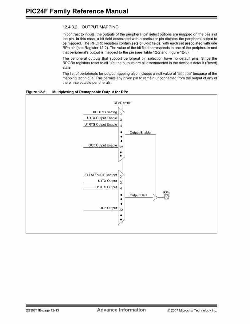
12.4.3.2 OUTPUT MAPPING
In contrast to inputs, the outputs of the peripheral pin select options are mapped on the basis ofthe pin. In this case, a bit field associated with a particular pin dictates the peripheral output tobe mapped. The RPORx registers contain sets of 6-bit fields, with each set associated with oneRPn pin (see Register 12-2). The value of the bit field corresponds to one of the peripherals andthat peripheral�s output is mapped to the pin (see Table 12-2 and Figure 12-5).
The peripheral outputs that support peripheral pin selection have no default pins. Since theRPORx registers reset to all �0�s, the outputs are all disconnected in the device�s default (Reset)state,
The list of peripherals for output mapping also includes a null value of �000000� because of themapping technique. This permits any given pin to remain unconnected from the output of any ofthe pin-selectable peripherals.
Figure 12-6: Multiplexing of Remappable Output for RPn
0
3
RPnR<5:0>
I/O TRIS Setting
U1TX Output Enable
U1RTS Output Enable 4
22OC5 Output Enable
0
3
I/O LAT/PORT Content
U1TX Output
U1RTS Output 4
22OC5 Output
Output Enable
Output DataRPn
DS39711B-page 12-13 Advance Information © 2007 Microchip Technology Inc.

Section 12. I/O PortsI/O
Ports
12
Table 12-2: Output Selection for Remappable Pin (RPn)
Table 12-3: Registers Associated with Output Function on RPn pin
12.4.3.3 MAPPING LIMITATIONS
The control schema of peripheral select pins is not limited to a small range of fixed peripheralconfigurations. There are no mutual or hardware enforced lockouts between any of the peripheralmapping SFRs; literally any combination of peripheral mappings across any or all of the RPn pinsis possible. This includes both many-to-one and one-to-many mappings of peripheral inputs andoutputs to pins. While such mappings may be technically possible from a configuration point ofview, the user must ensure the selected configurations are supportable from an electrical pointof view.
12.4.4 Controlling Configuration ChangesBecause peripheral remapping can be changed during run time, some restrictions on peripheralremapping are needed to prevent accidental configuration changes. PIC24F devices includethree features to prevent alterations to the peripheral map:
� Control register lock sequence� Continuous state monitoring� Configuration bit remapping lock
Function(1) RPnR<5:0> Output Name
NULL 0 The pin is an I/O Port pin.C1OUT 1 RPn tied to Comparator 1 Output.C2OUT 2 RPn tied to Comparator 2 Output.U1TX 3 RPn tied to UART1 Transmit.U1RTS 4 RPn tied to UART1 Ready To Send.U2TX 5 RPn tied to UART2 Transmit.U2RTS 6 RPn tied to UART2 Ready To Send.SDO1 7 RPn tied to SPI1 Data Output.SCK1OUT 8 RPn tied to SPI1 Clock Output.SS1OUT 9 RPn tied to SPI1 Slave Select Output.SDO2 10 RPn tied to SPI2 Data Output.SCK2OUT 11 RPn tied to SPI2 Clock Output.SS2OUT 12 RPn tied to SPI2 Slave Select Output.OC1 18 RPn tied to Output Compare 1.OC2 19 RPn tied to Output Compare 2.OC3 20 RPn tied to Output Compare 3.OC4 21 RPn tied to Output Compare 4.OC5 22 RPn tied to Output Compare 5.Note 1: The device may have more or less number of output functions. For actual details, please refer to the specific
device data sheet.
Pin Register Associated bits
RP0 RPO0<5:0> RP0R<5:0>RP1 RPO0<13:8> RP1R<5:0>RP2 RPO1<5:0> RP2R<5:0>RPn RPOn/2<5:0> RPnR<5:0>
RPn + 1 RPOn/2<13:8> RPn + 1R<5:0>Legend: n = 0, 2, 4, . . . , etc.
© 2007 Microchip Technology Inc. Advance Information DS39711B-page 12-14
PIC24F Family Reference Manual
12.4.4.1 CONTROL REGISTER LOCK
Under normal operation, writes to the RPINRx and RPORx registers are not allowed; attemptedwrites will appear to execute normally, but the contents of the registers will remain unchanged.To change these registers, they must be unlocked in hardware. The register lock is controlled bythe IOLOCK bit (OSCCON<6>). Setting IOLOCK prevents writes to the control registers; clearingIOLOCK allows writes.
To set or clear IOLOCK, a specific command sequence must be executed:
1. Write 46h to OSCCON<7:0>.2. Write 57h to OSCCON<7:0>.3. Clear (or set) IOLOCK as a single operation.
The unlock/lock sequence must be executed as an assembly language routine in the same man-ner as changes to the oscillator configuration because the unlock sequence is timing critical. Ifthe bulk of the application is written in C, or another high-level language, the unlock sequenceshould be performed by writing inline assembly or using built-in functions provided by theMPLAB® C30 C Complier.
IOLOCK remains in one state until changed. This allows all of the peripheral pin selects to beconfigured with a single unlock sequence, followed by an update to all control registers, thenlocked with a second lock sequence.
12.4.4.2 CONTINUOUS STATE MONITORING
In addition to being protected from direct writes, the contents of the RPINRx and RPORxregisters are constantly monitored in hardware by shadow registers. If an unexpected change inany of the registers occurs (such as cell disturbances caused by ESD or other external events),a configuration mismatch Reset will be triggered.
12.4.4.3 CONFIGURATION BIT PIN SELECT LOCK
As an additional level of safety, the device can be configured to prevent more than one writesession to the RPINRx and RPORx registers. The IOL1WAY (FOSC<IOL1WAY>) Configurationbit blocks the IOLOCK bit from being cleared after it has been set once.
In the default (unprogrammed) state, IOL1WAY is set, restricting users to one write session.Programming IOL1WAY allows users unlimited access (with the proper use of the unlocksequence) to the peripheral pin select registers.
12.4.5 Considerations for Peripheral Pin SelectionThe ability to control peripheral pin selection introduces several considerations into applicationdesign that should be considered.This is particularly true for several common peripherals whichare only available as remappable peripherals.
Before any other application code is executed, the user must initialize the device with the properperipheral configuration. Since the IOLOCK bit resets in the unlocked state, it is not necessaryto execute the unlock sequence after the device has come out of Reset. For the sake ofapplication safety, however, it is always a good idea to set IOLOCK and lock the configurationafter writing to the control registers.
Choosing the configuration requires the review of all peripheral pin selects and their pinassignments, especially those that will not be used in the application. In all cases, unusedpin-selectable peripherals should be disabled. Unused peripherals should have their inputsassigned to VSS. I/O pins with unused RPn functions should be configured with the NULL (�0�)peripheral output.
Note: MPLAB® C30 C Compiler provides built-in C language functions for unlocking theOSCCON register:__builtin_write_OSCCONL(value)__builtin_write_OSCCONH(value)
See �MPLAB C30 C Compiler User�s Guide� for more information.
DS39711B-page 12-15 Advance Information © 2007 Microchip Technology Inc.

Section 12. I/O PortsI/O
Ports
12
The assignment of a RPn pin to the peripheral input or output depends on the peripheral and itsuse in the application. It is better to be done immediately following device Reset and before theperipheral configuration.
The assignment of a peripheral output to a particular pin does not automatically perform anyother configuration of the pin�s I/O circuitry. This means adding a pin selectable output to a pinmay mean inadvertently driving an existing peripheral input when the output is driven. Usersmust be familiar with the behavior of other fixed peripherals that share a remappable pin. To besafe, fixed digital peripherals that share the same pin should be disabled when not in use.
Configuring a remappable pin for a specific peripheral input does not automatically turn thatfeature on. The peripheral must be specifically configured for operation and enabled, as if it weretied to a fixed pin.
A final consideration is that peripheral pin select functions neither override analog inputs, norreconfigure pins with analog functions for digital I/O. If a pin is configured as an analog input ondevice Reset, it must be explicitly reconfigured as digital I/O when used with a peripheral pinselect.
12.4.5.1 BASIC STEPS TO USE PERIPHERAL PIN SELECTION (PPS)
1. Disable any fixed digital peripherals on the pins to be used.2. Switch pins to be used for digital functionality (if they have analog functionality) using the
ADxPCFG register.3. Unlock the OSCCON register and clear bit, IOLOCK (not needed after device Reset).4. Set RPINRx and RPORx registers appropriately.5. Unlock the OSCCON register and set bit, IOLOCK, to �1�.6. Configure and enable newly mapped PPS peripherals.
Example 12-1 shows a configuration for bidirectional communication with flow control usingUART1. The following input and output functions are used:
� Input Functions: U1RX, U1CTS� Output Functions: U1TX, U1RTS
© 2007 Microchip Technology Inc. Advance Information DS39711B-page 12-16

PIC24F Family Reference Manual
Example 12-1: Configuring UART1 Input and Output Functions//*************************************************************// Unlock Registers//*************************************************************__builtin_write_OSCCONL(OSCCON & 0xbf) //clear the bit 6 of OSCCONL to
//unlock Pin Re-map//******************************************************************//This code is used when interested in inline assembly. If this code is //used then the above two lines should not be used for unlocking.//******************************************************************/*asm volatile ( �push w1 \n�
�push w2 \n��push w3 \n�"mov #OSCCON, w1 \n""mov #0x46, w2 \n""mov #0x57, w3 \n""mov.b w2, [w1] \n""mov.b w3, [w1] \n""bclr OSCCON, #6 \n"�pop w3 \n��pop w2 \n��pop w1�);
*///************************************************************// Configure Input Functions//************************************************************
//***************************// Assign U1Rx To Pin RP0//***************************RPINR18bits.U1RXR = 0; //�0� represents RP0
//***************************// Assign U1CTS To Pin RP1//***************************RPINR18bits.U1CTSR = 1; //�1� represents RP1
//************************************************************// Configure Output Functions//************************************************************
//***************************// Assign U1Tx To Pin RP2//***************************RPOR1bits.RP2R = 3; //�3� represents U1TX
//***************************// Assign U1RTS To Pin RP3//***************************RPOR1bits.RP3R = 4; //�4� represents U1RTS
//************************************************************// Lock Registers//************************************************************__builtin_write_OSCCONL(OSCCON | 0x40) //set the bit 6 of OSCCONL to
//lock Pin Re-map//******************************************************************//This code is used when interested in inline assembly. If this code is //used then the above two lines should not be used for unlocking.//******************************************************************/*asm volatile ( �push w1 \n�
�push w2 \n��push w3 \n�"mov #OSCCON, w1 \n""mov #0x46, w2 \n""mov #0x57, w3 \n""mov.b w2, [w1] \n""mov.b w3, [w1] \n""bset OSCCON, #6 \n"�pop w3 \n��pop w2 \n��pop w1�;
*/
DS39711B-page 12-17 Advance Information © 2007 Microchip Technology Inc.

Section 12. I/O PortsI/O
Ports
12
12.4.6 Peripheral Pin Select RegistersThese registers are used to configure input and output functionality of the PIC24F device pins.
� RPINRx: Peripheral Pin Select Input Register x� RPORy: Peripheral Pin Select Output Register y
Register 12-5: RPINRx: Peripheral Pin Select Input Register x(2)
Register 12-6: RPORy: Peripheral Pin Select Output Register y(2)
U-0 U-0 U-0 R/W-0 R/W-0 R/W-0 R/W-0 R/W-0� � Input Function bits<5:0>(1)
bit 15 bit 8
U-0 U-0 U-0 U-0 U-0 U-0 U-0 U-0� � Input Function bits<5:0>(1)
bit 7 bit 0
Legend:R = Readable bit W = Writable bit U = Unimplemented bit, read as �0�-n = Value at POR �1� = Bit is set �0� = Bit is cleared x = Bit is unknown
bit 15-14 Unimplemented: Read as �0� bit 13-8 Input Function Bits<5:0>: Assign Peripheral to Corresponding RPn Pin bits(1)
bit 7-6 Unimplemented: Read as �0� bit 5-0 Input Function Bits<5:0> Assign Peripheral to Corresponding RPn Pin bits(1)
Note 1: Here, �n� represents the peripheral select input pin number.2: Here, �x� represents the Peripheral Pin Select Input register number and it varies from device to device.
U-0 U-0 U-0 R/W-0 R/W-0 R/W-0 R/W-0 R/W-0� � RPnR<5:0>(1)
bit 15 bit 8
U-0 U-0 U-0 R/W-0 R/W-0 R/W-0 R/W-0 R/W-0� � RPnR<5:0>(1)
bit 7 bit 0
Legend:R = Readable bit W = Writable bit U = Unimplemented bit, read as �0�-n = Value at POR �1� = Bit is set �0� = Bit is cleared x = Bit is unknown
bit 15-14 Unimplemented: Read as �0� bit 13-8 RPnR<5:0>: Peripheral Output Function is Assigned to RPn Pin bits(1)
(see Table 12-2 for peripheral function numbers)bit 7-6 Unimplemented: Read as �0� bit 5-0 RPnR<5:0>: Peripheral Output Function is Assigned to RPn Pin bits(1)
(see Table 12-2 for peripheral function numbers)
Note 1: Here, �n� represents the peripheral pin select output pin number.2: Here, �y� represents the Peripheral Pin Select Output register number and it varies from device to device.
© 2007 Microchip Technology Inc. Advance Information DS39711B-page 12-18

PIC24F Family Reference Manual
12.5 PORT DESCRIPTIONSRefer to the specific device data sheet for a description of the available I/O ports, peripheralmultiplexing details and available peripheral pin select pins.
12.6 CHANGE NOTIFICATION (CN) PINSThe Change Notification (CN) pins provide PIC24F devices the ability to generate interruptrequests to the processor in response to a Change-of-State (COS) on selected input pins. Thetotal number of available CN inputs is dependent on the selected PIC24F device. Refer to thespecific device data sheet for further details.
Figure 12-7 shows the basic function of the CN hardware.
12.6.1 CN Control RegistersThere are four control registers associated with the CN module. The CNENx registers containthe CNxIE control bits, where �x� denotes the number of the CN input pin. The CNxIE bit must beset for a CN input pin to interrupt the CPU.
The CNPUx/CNPDx registers contain the CNxPUE/CNxPDE control bits. Each CN pin has aweak pull-up/pull-down device connected to the pin which can be enabled or disabled using theCNxPUE/CNxPDE control bits. The weak pull-up/pull-down devices act as a current source/sinkthat is connected to the pin and eliminate the need for external resistors when push button orkeypad devices are connected. Refer to the �Electrical Characteristics� section of the specificdevice data sheet for CN pull-up/pull-down device current specifications.
Figure 12-7: Input Change Notification Block Diagram
CN
D Q
C
D Q
C
CN0IE (CNEN1<0>)
CN0pin
CN0PUE(CNPU1<0>)
CN0 Change
CN1 Change
CNx Change
Interrupt
CN1-CNx(details notshown)
CN0PDE(CNPD1<0>)
VDD
DS39711B-page 12-19 Advance Information © 2007 Microchip Technology Inc.

Section 12. I/O PortsI/O
Ports
12
12.6.2 CN Configuration and OperationThe CN pins are configured as follows:
1. Ensure that the CN pin is configured as a digital input by setting the associated bit in theTRISx register.
2. Enable interrupts for the selected CN pins by setting the appropriate bits in the CNENxregisters.
3. Turn on the weak pull-up devices (if desired) for the selected CN pins by setting theappropriate bits in the CNPUx registers.
4. Clear the CNxIF interrupt flag.5. Select the desired interrupt priority for CN interrupts using the CNxIP<2:0> control bits.6. Enable CN interrupts using the CNxIE control bit.
When a CN interrupt occurs, the user should read the PORT register associated with the CNpin(s). This will clear the mismatch condition and set up the CN logic to detect the next pinchange. The current PORT value can be compared to the PORT read value obtained at the lastCN interrupt to determine the pin that changed.
The CN pins have a minimum input pulse-width specification. Refer to the �ElectricalCharacteristics� section of the specific device data sheet for further details.
12.6.3 CN Operation in Sleep and Idle ModesThe CN module continues to operate during Sleep or Idle mode. If one of the enabled CN pinschanges states, the CNxIF status bit will be set. If the CNxIE bit is set, the device will wake fromSleep or Idle mode and resume operation.
If the assigned priority level of the CN interrupt is equal to, or less than, the current CPU prioritylevel, device execution will continue from the instruction immediately following the SLEEP orIDLE instruction.
If the assigned priority level of the CN interrupt is greater than the current CPU priority level,device execution will continue from the CN interrupt vector address.
© 2007 Microchip Technology Inc. Advance Information DS39711B-page 12-20

PIC24F Family Reference Manual
12.7
REG
ISTE
R M
APS
A s
umm
ary
of th
e re
gist
ers
asso
ciat
ed w
ith th
e P
IC24
F I/O
por
ts is
pro
vide
d in
Tab
le12
-4, T
able
12-5
and
Tab
le12
-6.
Tabl
e 12
-4:
Spec
ial F
unct
ion
Reg
iste
rs A
ssoc
iate
d w
ith I/
O P
orts
(1)
Tabl
e 12
-5:
Spec
ial F
unct
ion
Reg
iste
rs A
ssoc
iate
d w
ith P
erip
hera
l Pin
Sel
ectio
n(1)
Tabl
e 12
-6:
Spec
ial F
unct
ion
Reg
iste
rs A
ssoc
iate
d w
ith C
hang
e N
otifi
catio
n Pi
ns(1
)
Nam
eB
it 15
Bit
14B
it 13
Bit
12B
it 11
Bit
10B
it 9
Bit
8B
it 7
Bit
6B
it 5
Bit
4B
it 3
Bit
2B
it 1
Bit
0A
ll R
eset
s
TRIS
xP
OR
Tx D
ata
Dire
ctio
n C
ontro
l bits
FFFF
LATx
PO
RTx
Dat
a La
tch
bits
xxxx
PO
RTx
Rx1
5R
x14
Rx1
3R
x12
Rx1
1R
x10
Rx9
Rx8
Rx7
Rx6
Rx5
Rx4
Rx3
Rx2
Rx1
Rx0
xxxx
OD
Cx
PO
RTx
Ope
n-D
rain
Con
trol b
its0000
Not
e1:
Ref
er to
the
spec
ific
devi
ce d
ata
shee
t for
the
I/O P
orts
regi
ster
map
det
ails
.
Nam
eB
it 15
Bit
14B
it 13
Bit
12B
it 11
Bit
10B
it 9
Bit
8B
it 7
Bit
6B
it 5
Bit
4B
it 3
Bit
2B
it 1
Bit
0A
ll R
eset
s
RP
INR
x�
�In
put F
unct
ion
bits
<5:0
>�
�In
put F
unct
ion
bits
<5:0
>3F3F
(2)
RP
OR
y�
�R
PnR
<5:0
>�
�R
PnR
<5:0
>0000
Not
e1:
Ref
er to
the
spec
ific
devi
ce d
ata
shee
t for
Per
iphe
ral P
in S
elec
t reg
iste
r map
det
ails
.2:
The
num
ber o
f bits
impl
emen
ted
varie
s w
ith th
e nu
mbe
r of p
ins
the
devi
ce h
as.
Nam
eB
it 15
Bit
14B
it 13
Bit
12B
it 11
Bit
10B
it 9
Bit
8B
it 7
Bit
6B
it 5
Bit
4B
it 3
Bit
2B
it 1
Bit
0A
ll R
eset
s
CN
ENx
Cha
nge
Not
ifica
tion
Inte
rrup
t Ena
ble
bits
0000
CN
PUx
Cha
nge
Not
ifica
tion
Pull-
up E
nabl
e bi
ts0000
CN
PDx
Cha
nge
Not
ifica
tion
Pull-
Dow
n En
able
bits
0000
Not
e1:
Ref
er to
the
spec
ific
devi
ce d
ata
shee
t for
Cha
nge
Not
ifica
tion
Pin
regi
ster
det
ails
.
DS39711B-page 12-21 © 2007 Microchip Technology Inc.
Section 12. I/O PortsI/O
Ports
12
12.8 RELATED APPLICATION NOTESThis section lists application notes that are related to this section of the manual. Theseapplication notes may not be written specifically for the PIC24F device family, but the conceptsare pertinent and could be used with modification and possible limitations. The currentapplication notes related to the I/O Ports with Peripheral Pin Select (PPS) are:
Title Application Note #Implementing Wake-up on Key Stroke AN552
Note: Please visit the Microchip web site (www.microchip.com) for additional applicationnotes and code examples for the PIC24F family of devices.
© 2007 Microchip Technology Inc. Advance Information DS39711B-page 12-22

PIC24F Family Reference Manual
12.9 REVISION HISTORY
Revision A (August 2006)This is the initial released revision of this document.
Revision B (May 2007)Added PPS section, removed JTAG boundary scan section and added PPS SFR table.
DS39711B-page 12-23 Advance Information © 2007 Microchip Technology Inc.

Section 12. I/O PortsI/O
Ports
12
NOTES:
© 2007 Microchip Technology Inc. Advance Information DS39711B-page 12-24