Embed Size (px)
Citation preview

Investigation of Large Strain Actuation in Barium Titanate
Thesis by
Eric Burcsu
In Partial Fulfillment of the Requirements
for the Degree of
Doctor of Philosophy
1 8 9 1
CA
LIF
OR
NIA
I
NS T IT U T E O F T
EC
HN
OL
OG
Y
Graduate Aeronautical Laboratories
California Institute of Technology
Pasadena, California
2001
(Defended May 15, 2001)

ii
c© 2001
Eric Burcsu
All Rights Reserved

iii
Dedicated to my parents

iv
ACKNOWLEDGMENTS
At an age when most young men have entered the world to make their fortune, I struggled
with mathematics, science and the mysteries of the natural world. Those were difficult days,
but days that I will look back upon with fond memories. There are many people, too many
to mention in these few paragraphs, who helped me to get to this point and succeed where
others have failed. I would like to take this opportunity to thank some of the people who
contributed most to my education.
I would like to thank my advisor Prof. Ravichandran for giving me the opportunity to
work on this project. He gave me advice and direction while allowing me the freedom to
develop the project according to my own vision. Without his advice and encouragement,
I would never have finished this quickly. I would also like to thank Prof. Bhattacharya
for acting as my second advisor. He gave the motivation for the project and helped me
considerably along the way. I would like to thank Prof. Rosakis, Prof. Ortiz, and Prof. Haile
for graciously agreeing to be members of my thesis committee. I also owe my appreciation
to Dr. Yi-Chung Shu and Dr. Jiangyu Li for their discussions that greatly helped my
understanding of the subject.
The many past and present members of Prof. Ravichandran’s research group have lent
their knowledge and experience, and given me many suggestions that saved weeks of trial
and error in perfecting the experimental setup and procedure. In particular, I would like to
express my gratitude to Shiming Zhuang, Jun Lu, Dr. Kenji Oguni, and Dr. Sangwook Lee
for their help. I would also like to thank other past and present members of the GALCIT
community, specifically, Dr. Pradeep Guduru, Dr. Hansuk Lee, and Dr. Demir Coker for
their helpful suggestions. Thanks are also due to Petros Arakelian for his assistance.
I would like to thank the many friends who made my stay at Caltech almost bearable,
most of whom I have known since I first arrived at Caltech. My experience would not
be complete without a well-balanced, daily meal from the Chandler Dining Facility and

v
“intellectual” conversations with my lunch-time companions Dr. Lavi Zuhal, Dr. Sandeep
“Deep” Sane, Ioannis Chasiotis, and Dr. Benjamin Chow. Dr. Zuhal deserves special recog-
nition for his continuous lunch attendance over the past five years. I would like to thank
my biking friends David Anderson and Dr. Adam Rasheed for keeping me in good physical
shape during my stay here. I’ve been lucky to have so many close friends at Caltech. I will
miss all of them greatly.
Few people have had such a great influence on my personal and scientific development
than Nitin “Desh” Deshpande. Desh, a native Punenian, who is very proud of his Puneni-
anity, has been a continuous inspiration to all of us. As an Aeronautical Engineer, he has
made significant contributions to the “aircraft air-conditioning” industry. As a vegetarian,
he introduced me to the wonders of “Punenian veggie,” as well as many other aspects of
Punenian food and culture.
There are many others outside the Caltech community who contributed to my success.
I could not have gotten this far in my education without the help and support of my family.
From the beginning, my father and mother encouraged me excel and achieve all the goals
that I set for myself, while my sister, Theresa, inspired me to do well. Without their en-
couragement I would never have made it this far. My father often told me that there is no
disadvantage to having additional education. This helped convince me to continue beyond
the Master’s degree and become the second doctor in the family. I would also like to thank
Prof. Fuh-Gwo Yuan of N.C. State for encouraging me to come to Caltech rather than that
“other institute” on the east coast. I think it was a good decision. Finally, I cannot fail to
mention my fiance, Young, who made the past two years so special. She gave me a reason
to finish school and finally enter the real world.
I would like to thank the Army Research Office (Dr. M. A. Zikry, Program Manager) as well
as the National Science Foundation, through the MRSEC program, for financial support of
this project. I would also like to thank the Department of Defense and Army Research Office
for supporting me for three years through the National Defense Science and Engineering
Graduate Fellowship program.

vi
ABSTRACT
Sensors and actuators based on ferroelectric materials have become indispensable in
the fields of aerospace, high technology, and medical instruments. Most devices rely on
the linear piezoelectric behavior of formulations of PZT which offer high bandwidth, linear
actuation but very low strains of around 0.1%. The nonlinear electromechanical behavior
of these materials is largely governed by the motion of domains and is highly affected by
stress as well as electric field. The recent theories of Shu and Bhattacharya have sought
to address some of the issues related to the structure and behavior of these materials at
the mesoscale. One result of the theories is the prediction of another mode of actuation
in ferroelectric crystals based on a combined electrical and mechanical loading that could
result in strains of up to 6%.
A description of the phenomenological theories of ferroelectrics are presented including
the classical Landau-Ginsburg-Devonshire theory and the more recent theory of Shu and
Bhattacharya. Predictions are made, based on the theory, of the electromechanical behavior
of ferroelectric crystals that are addressed by the experiments. An experimental setup has
been designed to investigate large strain actuation in single crystal ferroelectrics based on
combined electrical and mechanical loading. An investigation of the stress dependence of
the electrostrictive response has been carried out with in situ observations of the domain
patterns under constant compressive stress and variable electric field. Experiments have
been performed on initially single domain crystals of barium titanate (BaTiO3) with (100)
and (001) orientation at compressive stresses between 0 and 5 MPa. Global strain and

vii
polarization histories have been recorded. The electrostrictive response is shown to be
highly dependent on the level of applied stress with a maximum strain of 0.9% measured at
a compressive stress of about 2 MPa. An unusual secondary hysteresis has been observed
in the polarization signal at high levels of stress that indicates an intermediate structural
configuration, possibly the orthorhombic state. Polarized light microscopy has been used to
observe the evolution of the domain pattern simultaneously with the strain and polarization
measurement. These results are discussed and suggestions for future work are proposed.

viii
Contents
ACKNOWLEDGMENTS iv
ABSTRACT vi
1 INTRODUCTION 1
1.1 Motivation . . . . . . . . . . . . . . . . . . . . . . . . . . . . . . . . . . . . 1
1.2 Background . . . . . . . . . . . . . . . . . . . . . . . . . . . . . . . . . . . . 3
1.2.1 Ferroelectric Materials . . . . . . . . . . . . . . . . . . . . . . . . . . 3
1.2.2 Piezoelectricity and Electrostriction . . . . . . . . . . . . . . . . . . 5
1.2.3 Domain Switching and the Enhanced Electromechanical Response . 11
1.3 Outline . . . . . . . . . . . . . . . . . . . . . . . . . . . . . . . . . . . . . . 13
References . . . . . . . . . . . . . . . . . . . . . . . . . . . . . . . . . . . . . . . . 15
2 THEORY 18
2.1 Overview . . . . . . . . . . . . . . . . . . . . . . . . . . . . . . . . . . . . . 18
2.2 Landau-Ginsburg-Devonshire Theory . . . . . . . . . . . . . . . . . . . . . . 18
2.3 Finite Deformation Theory . . . . . . . . . . . . . . . . . . . . . . . . . . . 22
2.4 Flat Plate Configuration . . . . . . . . . . . . . . . . . . . . . . . . . . . . . 24
2.5 Mode of Electrostrictive Actuation . . . . . . . . . . . . . . . . . . . . . . . 29
References . . . . . . . . . . . . . . . . . . . . . . . . . . . . . . . . . . . . . . . . 31
3 EXPERIMENTAL METHOD 32

ix
3.1 Overview . . . . . . . . . . . . . . . . . . . . . . . . . . . . . . . . . . . . . 32
3.2 Material . . . . . . . . . . . . . . . . . . . . . . . . . . . . . . . . . . . . . . 32
3.3 Load Mechanism . . . . . . . . . . . . . . . . . . . . . . . . . . . . . . . . . 33
3.4 Strain Measurement . . . . . . . . . . . . . . . . . . . . . . . . . . . . . . . 35
3.5 Electrical System . . . . . . . . . . . . . . . . . . . . . . . . . . . . . . . . . 38
3.5.1 Electrodes . . . . . . . . . . . . . . . . . . . . . . . . . . . . . . . . . 38
3.5.2 High-Voltage System . . . . . . . . . . . . . . . . . . . . . . . . . . . 39
3.6 Polarized-Light Microscopy . . . . . . . . . . . . . . . . . . . . . . . . . . . 41
3.6.1 Birefringence Contrast . . . . . . . . . . . . . . . . . . . . . . . . . . 42
3.6.2 Illumination and Charge Coupled Device (CCD) Sensor . . . . . . . 43
3.6.3 Mechanical System . . . . . . . . . . . . . . . . . . . . . . . . . . . . 45
3.6.4 Video System . . . . . . . . . . . . . . . . . . . . . . . . . . . . . . . 48
3.7 Instrumentation . . . . . . . . . . . . . . . . . . . . . . . . . . . . . . . . . . 49
3.8 Limitations . . . . . . . . . . . . . . . . . . . . . . . . . . . . . . . . . . . . 51
References . . . . . . . . . . . . . . . . . . . . . . . . . . . . . . . . . . . . . . . . 54
4 RESULTS 55
4.1 Overview . . . . . . . . . . . . . . . . . . . . . . . . . . . . . . . . . . . . . 55
4.2 Global Measurements . . . . . . . . . . . . . . . . . . . . . . . . . . . . . . 55
4.2.1 (100) Oriented Crystal . . . . . . . . . . . . . . . . . . . . . . . . . . 56
4.2.2 (001) Oriented Crystals . . . . . . . . . . . . . . . . . . . . . . . . . 57
4.2.3 Actuation Performance . . . . . . . . . . . . . . . . . . . . . . . . . 59
4.3 Frequency Response . . . . . . . . . . . . . . . . . . . . . . . . . . . . . . . 63
4.4 Polarized-Light Microscopy Observations . . . . . . . . . . . . . . . . . . . . 63

x
4.5 Damage Mechanisms . . . . . . . . . . . . . . . . . . . . . . . . . . . . . . . 66
4.6 Summary . . . . . . . . . . . . . . . . . . . . . . . . . . . . . . . . . . . . . 67
References . . . . . . . . . . . . . . . . . . . . . . . . . . . . . . . . . . . . . . . . 85
5 CONCLUSIONS 86
5.1 Suggestions for Future Work . . . . . . . . . . . . . . . . . . . . . . . . . . 87
References . . . . . . . . . . . . . . . . . . . . . . . . . . . . . . . . . . . . . . . . 92
Bibliography 93

xi
List of Figures
1.1 Two important figures of merit for common microactuator systems. . . . . . 2
1.2 Polarization-electric field hysteresis for ferroelectric materials. . . . . . . . . 4
1.3 Phases of barium titanate. . . . . . . . . . . . . . . . . . . . . . . . . . . . . 5
1.4 Structure of barium titanate. . . . . . . . . . . . . . . . . . . . . . . . . . . 6
1.5 Subgranular domain structure. . . . . . . . . . . . . . . . . . . . . . . . . . 6
1.6 The converse piezoelectric effect. . . . . . . . . . . . . . . . . . . . . . . . . 9
1.7 Electrostrictive behavior of dielectrics. . . . . . . . . . . . . . . . . . . . . . 9
1.8 Schematic diagram of the poling process for ferroelectric ceramics. . . . . . 11
1.9 Schematic diagram of a piezoelectric cofired multilayer ‘stack’ actuator. . . 12
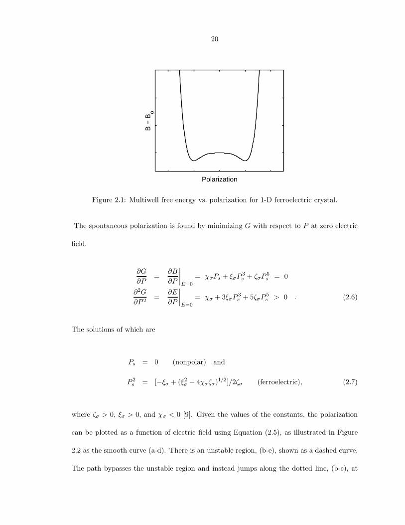
2.1 Multiwell free energy vs. polarization for 1-D ferroelectric crystal. . . . . . . 20
2.2 Polarization vs. electric field calculated using the Landau-Ginsburg method
for a 1-D ferroelectric crystal. . . . . . . . . . . . . . . . . . . . . . . . . . . 21
2.3 Continuum model of a ferroelectric crystal. . . . . . . . . . . . . . . . . . . 23
2.4 Flat plate ferroelectric crystal with electrodes on two faces. . . . . . . . . . 25
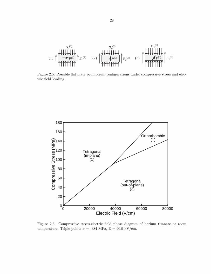
2.5 Possible flat plate equilibrium configurations under compressive stress and
electric field loading. . . . . . . . . . . . . . . . . . . . . . . . . . . . . . . . 28
2.6 Compressive stress-electric field phase diagram of barium titanate at room
temperature. . . . . . . . . . . . . . . . . . . . . . . . . . . . . . . . . . . . 28
2.7 Mode of operation of an actuator based on combined electromechanical load-
ing of a ferroelectric single crystal. . . . . . . . . . . . . . . . . . . . . . . . 30

xii
2.8 Schematic bipolar phase diagram. . . . . . . . . . . . . . . . . . . . . . . . . 30
3.1 Schematic diagram of experimental setup and specimen dimensions. . . . . 33
3.2 Photographs of the experimental setup. . . . . . . . . . . . . . . . . . . . . 34
3.3 Loading frame for constant load experiments on ferroelectric single crystals. 36
3.4 Closeup of experimental setup showing load cross member, specimen, loading
platens, and LVDT actuation beam. . . . . . . . . . . . . . . . . . . . . . . 37
3.5 Photograph of experimental setup detailing displacement measurement and
specimen location. . . . . . . . . . . . . . . . . . . . . . . . . . . . . . . . . 38
3.6 Block diagram of high-voltage system. . . . . . . . . . . . . . . . . . . . . . 41
3.7 Charge signal before and after removing the exponential decay. . . . . . . . 42
3.8 (a) Generation of birefringence contrast in tetragonal barium titanate and
(b) intensity vs. domain thickness, d, with 632 nm illumination. . . . . . . . 43
3.9 Spectrum of the quartz halogen fiber optic illuminator . . . . . . . . . . . . 44
3.10 Spectral responsivity of Sony XC-75 CCD camera . . . . . . . . . . . . . . . 45
3.11 Predicted relative intensity vs. 90 domain thickness. . . . . . . . . . . . . . 46
3.12 Schematic diagram of long working distance polarizing microscope. . . . . . 47
3.13 Dimensions of extension tube for microscope for use with Nikon 210 mm tube
length objectives and C-mount camera. . . . . . . . . . . . . . . . . . . . . 47
3.14 Video image distortion caused by interlaced fields. . . . . . . . . . . . . . . 49
3.15 Flow chart of instrumentation system. . . . . . . . . . . . . . . . . . . . . . 52
3.16 FFT of LVDT signal illustrating vibrational modes of the actuation lever. . 53
4.1 (a) Electric field and strain vs. time and (b) strain vs. electric field for (100)
oriented crystal at 1.07 MPa compressive stress. . . . . . . . . . . . . . . . . 68

xiii
4.2 (a) Electric field and polarization vs. time and (b) polarization vs. electric
field for (100) oriented crystal at 1.07 MPa compressive stress. . . . . . . . 69
4.3 Strain vs. electric field for five values of compressive stress with an initially
(100) oriented crystal with input amplitude of ±10 kV/cm. . . . . . . . . . 70
4.4 Polarization vs. electric field for five values of compressive stress with an
initially (100) oriented crystal with input amplitude of ±10 kV/cm. . . . . 71
4.5 Strain vs. polarization for five values of compressive stress with an initially
(100) oriented crystal with input amplitude of ±10 kV/cm. . . . . . . . . . 72
4.6 Strain vs. electric field for six values of compressive stress with an initially
(001) oriented crystal with input amplitude of ±7.5 kV/cm. . . . . . . . . . 73
4.7 Polarization vs. electric field for six values of compressive stress with an
initially (001) oriented crystal with input amplitude of ±7.5 kV/cm. . . . . 74
4.8 Strain vs. polarization for six values of compressive stress with an initially
(001) oriented crystal with input amplitude of ±7.5 kV/cm. . . . . . . . . . 75
4.9 Primary (Ps1) and secondary (Ps2) spontaneous polarization . . . . . . . . . 76
4.10 Actuation strain vs. compressive stress for barium titanate. . . . . . . . . . 77
4.11 Coercive field vs. compressive stress for barium titanate. . . . . . . . . . . . 77
4.12 Derivative of strain with respect to electric field for (100) oriented crystal at
1.07 MPa compressive stress. . . . . . . . . . . . . . . . . . . . . . . . . . . 78
4.13 Comparison of predicted equilibrium phase diagram and experimental satu-
ration and desaturation of strain with respect to electric field. . . . . . . . . 78
4.14 Work per unit volume (per actuation stroke) vs. compressive stress. . . . . 79
4.15 Strain response at frequencies from 0.05 to 1.0 Hz with (a) 1.07 MPa and (b)
2.14 MPa compressive stress. . . . . . . . . . . . . . . . . . . . . . . . . . . 80

xiv
4.16 Sample images of domain patterns from experiment at 1.07 MPa compressive
stress with corresponding strain and polarization. . . . . . . . . . . . . . . . 81
4.17 Comparison of integrated image intensity and strain vs. electric field at five
stress levels. . . . . . . . . . . . . . . . . . . . . . . . . . . . . . . . . . . . . 82
4.18 Comparison of integrated image intensity and polarization (absolute value)
vs. electric field at five stress levels. . . . . . . . . . . . . . . . . . . . . . . . 83
4.19 Pictures of damaged crystals after experiments. . . . . . . . . . . . . . . . . 84
4.20 Spark path through initially polydomain crystal along a crack face. . . . . . 84

xv
List of Tables
1.1 Properties of barium titanate. . . . . . . . . . . . . . . . . . . . . . . . . . . 7
3.1 List of microscope components. . . . . . . . . . . . . . . . . . . . . . . . . . 48
3.2 List of instruments. . . . . . . . . . . . . . . . . . . . . . . . . . . . . . . . . 51
5.1 Ferroelectric and antiferroelectric perovskites. . . . . . . . . . . . . . . . . . 91

1
Chapter 1 INTRODUCTION
1.1 Motivation
An active or “smart” material is often defined as one that gives an unexpected response
to an input, for example, an electrical or magnetic response to a mechanical or thermal
input [1]. In the fields of mechanical and aerospace engineering, smart or active materials
of interest are those which can be incorporated into solid-state sensors or actuators. Ac-
tuators which produce a mechanical response to an electrical, magnetic or thermal input
can be used to replace existing servo mechanisms at lower size and weight or be used in
applications where traditional actuators are either too bulky, inaccurate or slow, such as
active damping, ultrasonics, nanopositioning, and MEMS. A number of such materials exist
including piezoelectrics, magnetostrictors, and shape memory alloys. A comparison of two
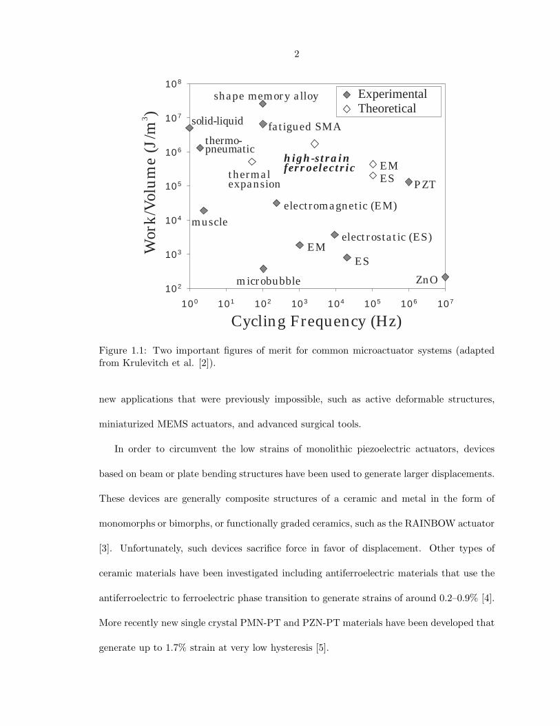
figures of merit (work per unit volume and cycling frequency) for a number of actuator
systems is shown in Figure 1.1, adapted from Krulevitch et al. [2].
Each actuator system shown in Figure 1.1 is ideal for certain applications. For instance,
piezoelectric materials, such as PZT, are ideal for applications requiring high frequency
response, such as ultrasonics for medical imaging or sonar, or precise displacement, such as
nanopositioning for fiber optic alignment or probe microscopy. These materials have the
added advantage that they can be used as sensors as well as actuators allowing feedback
control. The limitation of the materials, however, is that they can only produce very
small strains, up to about 0.1%. An increased strain level would open a wide range of
2
100 101 102 103 104 105 106 107
Cycling Frequency (Hz)
102
103
104
105
106
107
108
Wor
k/V
olu
me
(J/m
)3
m icr obubble ZnO
muscle
solid-liquid
thermo-pneumatic
P ZT
h igh -st r a i nfer r oelect r ic
t herma lexpansion
shape memor y a lloy
fa t igued SMA
elect romagnet ic (EM)
elect r osta t ic (ES)EM
ES
EMES
ExperimentalTheoretical
Figure 1.1: Two important figures of merit for common microactuator systems (adaptedfrom Krulevitch et al. [2]).
new applications that were previously impossible, such as active deformable structures,
miniaturized MEMS actuators, and advanced surgical tools.
In order to circumvent the low strains of monolithic piezoelectric actuators, devices
based on beam or plate bending structures have been used to generate larger displacements.
These devices are generally composite structures of a ceramic and metal in the form of
monomorphs or bimorphs, or functionally graded ceramics, such as the RAINBOW actuator
[3]. Unfortunately, such devices sacrifice force in favor of displacement. Other types of
ceramic materials have been investigated including antiferroelectric materials that use the
antiferroelectric to ferroelectric phase transition to generate strains of around 0.2–0.9% [4].
More recently new single crystal PMN-PT and PZN-PT materials have been developed that
generate up to 1.7% strain at very low hysteresis [5].

3
The current study has both an applied and scientific objective. The first, which ad-
dresses the issues mentioned above, is to demonstrate the use of a combined electrical and
mechanical loading condition to generate a large strain cycle in a ferroelectric single crystal.
Strains of 1.1% were predicted for barium titanate, a common ferroelectric material. Re-
sults of experiments on this material are presented in the following chapters. Larger strains
of up to 6% are predicted for other materials. The scientific objective is to gain a better
understanding of the mechanics of ferroelectrics by studying the single crystal behavior un-
der electrical and mechanical loading conditions. The information gained can be used by
others to validate existing models and develop better models of ferroelectric crystals and
ceramics.
1.2 Background
1.2.1 Ferroelectric Materials
The term ‘ferroelectric’ relates not to a relationship of the material to the element iron,
but simply a similarity of the properties to those of ferromagnets: just as ferromagnets ex-
hibit a spontaneous, reversible magnetization and an associated hysteresis behavior between
magnetization and magnetic field, ferroelectrics exhibit a spontaneous, reversible electrical
polarization and an associated hysteresis behavior between polarization and electric field [6].
Likewise, much of the terminology associated with ferroelectrics is borrowed from ferromag-
nets, for instance, the transition temperature below which the material exhibits ferroelectric
behavior is referred to as the Curie temperature. Other terminology is best introduced by
examining the typical polarization-electric field hysteresis curve for a ferroelectric mate-
rial, shown in Figure 1.2. The spontaneous polarization, Ps, is defined from this curve

4
Electric Field
Pol
ariz
atio
n
Ps
Ec
Pr
Figure 1.2: Polarization-electric field hysteresis for ferroelectric materials. The spontaneouspolarization (Ps) is defined by the line extrapolated from the saturated linear region to thepolarization axis. Remanent polarization (Pr) is the polarization remaining at zero electricfield. Coercive field (Ec) is the field required to reduce the polarization to zero.
by the extrapolation of the linear region at saturation back to the polarization axis. The
remaining polarization when the electric field returns to zero, is known as the ‘remanent po-
larization,’ Pr. Finally, the electric field at which the polarization returns to zero is known
as the ‘coercive field,’ Ec. The ferroelectric phenomenon was first discovered in Rochelle
salt (NaKC4H4O6·4H2O) in 1921 [7]. Other examples of ferroelectric materials include lead
titanate (PbTiO3), lithium niobate (LiNbO3), and, the material being examined in this
study, barium titanate (BaTiO3).
Barium titanate is a ferroelectric material of the perovskite class and has been ex-
tensively studied [6]. It exhibits four phases, shown in Figure 1.3: cubic, tetragonal, or-
thorhombic, and rhombohedral. The high temperature cubic phase is nonpolar while the
lower temperature phases are polar and ferroelectric. At high temperature it has the cubic
perovskite structure, as shown in Figure 1.4. When cooled below 120C, it transforms to

5
Temperature
NonpolarCubic
<100> PolarizedTetragonal
<110> PolarizedOrthorhombic
<111> PolarizedRhombohedral
-90oC 5oC 120oC
Figure 1.3: Phases of barium titanate. The arrow indicates the direction of polarization.
a tetragonal phase. The dimensions of the unit cell are distorted along the c-axis with a
ratio, c/a = 1.011, resulting in a spontaneous strain of 1.1%. In addition to the strain
induced by the lattice distortion, there is a spontaneous polarization along the axis of the
unit cell as indicated in the figure. Thus, at phase transition, the unit cell can take any
of six crystallographically equivalent combinations of strain and polarization. Furthermore,
different regions of a single crystal, or single grain in a polycrystal, can take on different
directions of polarization. A region of constant polarization is known as a ferroelectric do-
main. Domains are separated by 90 or 180 domain boundaries, as shown in Figure 1.5,
which can be nucleated or moved by electric field or stress (the ferroelastic effect). The
process of changing the polarization direction of a domain by nucleation and growth or wall
motion is known as domain switching. Electric field can induce both 90 or 180 switching,
while stress can induce only 90 switching. Some of the properties of single crystal barium
titanate are listed in Table 1.1.
1.2.2 Piezoelectricity and Electrostriction
Piezoelectricity is a property of ferroelectric, as well as many nonferroelectric crystals,
such as quartz, whose crystal structures satisfy certain symmetry criteria [10]. It also exists

6
(a)
Pol
ariz
atio
n
c
a
O2-
Ba2+
Ti4+
cubic tetragonal
c
a= 1.011
(b)
Figure 1.4: (a) The cubic (high temperature) and tetragonal (room temperature) structuresof barium titanate. The tetragonal structure has both an induced strain and polarization.(b) Upon the cubic to tetragonal phase transition, the unit cell can take any of six equivalentcombinations of strain and polarization. The arrow indicates the direction of polarization.
180o boundary
90o boundary
(a) (b)
Figure 1.5: (a) Schematic diagram of the subgranular structure of domains, or regions ofconstant polarization, separated by 90 or 180 boundaries. (b) Domain pattern in singlecrystal barium titanate photographed using a polarizing microscope.

7
Table 1.1: Properties of barium titanate.
Property ValueDensity (20C): ρ = 6.02 × 10³ kg/m3
cubic (120C): a = 3.996 AUnit Cell tetragonal (20C): a = 3.9920 A, c = 4.0361 A
Dimensions orthorhombic (-10C): a = 3.990 A, b = 5.669 A, c = 5.682 Arhombohedral (-168C): a = 4.001 A, α = 8951′
tetragonal (25C): Ps = 0.25–0.26 C/m2
Spontaneousorthorhombic (0C): Ps ≈ 0.21 C/m2 †
Polarizationrhombohedral (-100C): Ps ≈ 0.19 C/m2 †
Refractive Index na = 2.4Birefringence (20C): ∆n = −0.073
Elastic Constants
Stiffness (GPa):
CE11: 211CE
33: 160CE
12: 107CE
13: 114CE
44: 56.2CE
66: 127(at 25C, constant
electric field)∗
Compliance:(×10−3/GPa)
SE11: 8.01SE
33: 12.8SE
12: -1.57SE
13: -4.60SE
44: 17.8SE
66: 7.91
Piezoelectric
Strain (10−12C/N):(εj = dijEi)
d15: 580d31: -50.0d31: 106
Constants(at 25C)∗
Stress (C/m2):(σj = eijEi)
e15: 32.6e31: -3.88e31: 5.48
Dielectric Constant(constant strain)∗
(25C):εs11/εo: 1980εs33/εo: 48
† along pseudocubic directionSources: [8], [6], ∗[9]

8
in certain ceramic materials that either have a suitable texture or exhibit a net spontaneous
polarization. The direct piezoelectric effect is defined as a linear relationship between stress
and electric displacement or charge per unit area, as expressed by the equation
Di = dijkσjk , (1.1)
where σ is the stress tensor and D is the electric displacement vector which is related to
the polarization, P , by
Di = Pi + εoEi , (1.2)
where εo is the permittivity of free space and E is the electric field vector [11]. For materials
with large spontaneous polarizations, such as ferroelectrics, the electric displacement is
approximately equal to the polarization (D ≈ P ).
For actuators, a more common representation of piezoelectricity is that of the converse
piezoelectric effect. This is a linear relationship between strain and electric field, as shown
in Figure 1.6 and in the following equation at constant stress,
εij = dijkEk , (1.3)
where ε is the strain tensor and d is the same as in Equation (1.1). These relationships are
often expressed in a matrix notation
Di = dijσj (1.4)
εj = dijEi (1.5)
σj = eijEi , (1.6)

9
E
ε
E
Figure 1.6: Piezoelectricity, described by the converse piezoelectric effect, is a linear rela-tionship between strain and electric field.
± Eε
E
Figure 1.7: Electrostriction is a quadratic relationship between strain and electric field, ormore generally, an electric field induced deformation that is independent of field polarity.
where e is the matrix of piezoelectric stress constants [7, 10].
Electrostriction, in its most general sense, means simply ‘electric field induced defor-
mation’ [1]. However, the term is most often used to refer to an electric field induced
deformation that is proportional to the square of the electric field, as illustrated in Figure
1.7 and expressed by
εij = MijklEkEl . (1.7)
This effect does not require a net spontaneous polarization and, in fact, occurs for all
dielectric materials [7]. The effect is quite pronounced in some ferroelectric ceramics, such as
Pb(MgxNb1−x)O3 (PMN), which generate strains as large as those of piezoelectric PZT. For
the purposes of this dissertation, the term electrostriction will be defined in a more general
sense as electric field induced deformation that is independent of electric field polarity.

10
As mentioned earlier, piezoelectricity exists in polycrystalline ceramics which exhibit a
net spontaneous polarization. For a ferroelectric ceramic, while each grain may be micro-
scopically polarized, the overall material will not be, due to the random orientation of the
grains [10, 12]. For this reason, the ceramic must be poled under a strong electric field,
often at elevated temperature, in order to generate the net spontaneous polarization. This
process is illustrated in Figure 1.8 which shows a ferroelectric ceramic material in its un-
poled state with grains of random polarization. The ceramic is exposed to a strong electric
field generating an average polarization, P . Likewise the material can be depoled by electric
field or stress.
Poling involves the reorientation of domains within the grains. In the case of PZT
it may also involve polarization rotations due to phase changes. PZT is a solid solution
of lead zirconate and lead titanate that is often formulated near the boundary between
the rhombohedral and tetragonal phases (the morphotropic phase boundary). For these
materials, additional polarization states are available as it can choose between any of the
〈100〉 polarized states of the tetragonal phase, the 〈111〉 polarized states of the rhombohedral
phase, and the 〈11k〉 polarized states of the newly discovered monoclinic phase. The final
polarization of each grain, however, is constrained by the mechanical and electrical boundary
conditions presented by the adjacent grains. Due to residual stresses and grain boundary
mismatch, the poling process is extremely difficult to model and is an active subject of
research.
The complexity of the poling process is compounded when a ceramic actuator structure
is considered. A commonly used piezoelectric actuator design is the cofired multilayer or
‘stack’ actuator. The design consists of multiple ceramic layers with embedded electrodes.
This allows a large electric field to be applied to each layer, thus increasing the displace-

11
Figure 1.8: Schematic diagram of the poling process for ferroelectric ceramics, such as PZT.Poling generates a net polarization, P , which is necessary to make the ceramic piezoelectric.Poling is often performed at elevated temperature.
ment without increasing the driving voltage [1, 13]. Such actuators are often produced
with electrodes terminating inside the ceramic at one edge, as shown in Figure 1.9. Such
an arrangement is convenient from a manufacturing standpoint, but introduces some prob-
lems. In the area of the terminated electrode, the electric fields will be highly nonuniform,
complicating the poling process. These areas are subject to nonuniform stresses as well,
often leading to fatigue and the onset of failure in these regions. A better understanding of
the poling process including the stress effects on domain reorientation will lead to improved
design and reliability of these devices.
1.2.3 Domain Switching and the Enhanced Electromechanical Response
Apart from its importance to the poling process in ferroelectric ceramics, domain switch-
ing has a strong influence on the enhanced electromechanical response of some materials.
For instance, for 90 domain switching in barium titanate there is an associated strain of up
to 1.1%. This value is up to 6% for other materials. This process is believed to contribute to

12
CeramicMaterial
EmbeddedElectrode
Figure 1.9: Schematic diagram of a piezoelectric cofired multilayer ‘stack’ actuator.
the electromechanical response of PZT and may explain its increased piezoelectric response
relative to other ceramics [14].
A similar mechanism has been proposed to explain the enhanced electromechanical
response of single crystal relaxor materials. These materials are solid solutions of formu-
lations Pb(ZnxNb1−x)O3–PbTiO3 (PZN-PT) and Pb(MgxNb1−x)O3–PbTiO3 (PMN-PT),
which like PZT, are formulated near the morphotropic phase boundary. The proposed
mechanism is a reorientation of the polarization vector from the rhombohedral 〈111〉 direc-
tion to the 〈001〉 direction. Similar observations have been made in rhombohedral barium
titanate with electric fields along the [001] direction [15, 16]. Computational investigations
of the mechanism of polarization rotation have also been performed by Fu and Cohen using
an atomistic approach that seem to corroborate this hypothesis [17].
There have been a number of experimental and theoretical studies devoted to the sub-
ject of domain switching for both ceramics and single crystals [18]. The combined effect of
stress and electric field on PLZT ceramics was studied by Lynch by measuring the nonlinear
electromechanical response in presence of a uniaxial stress [19, 20]. Both strain and polar-
ization were measured as a function of electric field at different stress levels. It was found

13
that the magnitude of the strain increased with applied stress. In addition, there have been
many single crystal studies to understand the fundamental mechanisms governing domain
switching and avoid the inherent complexity of the polycrystal system; however, these stud-
ies were generally performed using electrical loading in the absence of stress [21, 22]. Stress
induced, 90 domain switching was observed by Li et al. in BaTiO3 and PbTiO3, however
their experiments were done with only mechanical loading [23]. They used a loading mecha-
nism to generate a compressive stress along the c-axis of a crystal and observed the domain
switching behavior using micro-Raman spectroscopy. For barium titanate, 90 domains
were shown to be nucleated by a compressive stress of 0.22 MPa. Removal of 90 domains
was initiated at a stress of 1.1 MPa. The current investigation includes combined electrical
and mechanical loading of barium titanate single crystals in an attempt to understand the
coupling of the two loading mechanisms and its relation to the subsequent electrostrictive
response.
1.3 Outline
The motivation for the current work and an introduction to the field of ferroelectric ma-
terials and the principles of piezoelectricity and electrostriction have been presented in this
chapter. Chapter 2 will describe the phenomenological theories that have been developed to
describe ferroelectric materials. The theory of Devonshire, based on the Landau-Ginsburg
theory of phase transitions, will be described along with the recent theory of Shu and Bhat-
tacharya which incorporates finite deformations. A simplified version of the theory will be
used to explain the principles of the experiments that have been performed. The exper-
imental setup and procedure are explained in Chapter 3. A mechanism is described for
applying constant compressive load and variable electric field to a ferroelectric crystal that

14
allows measurement of strain and polarization, as well as real time in situ observation of
the domain patterns. Results of experiments on single domain (100) and (001) oriented
barium titanate crystals are presented in Chapter 4. Finally, Chapter 5 summarizes the
contributions of this research and makes recommendations for future work.

15
References
[1] K. Uchino, Ferroelectric Devices, Marcel Decker, New York, 2000.
[2] P. Krulevitch, A. P. Lee, P. B. Ramsey, J. C. Trevino, J. Hamilton, and M. A. Northrup,
“Thin film shape memory alloy microactuators,” J. MEMS 5(4), pp. 270–282, 1996.
[3] G. H. Haertling, “Rainbow ceramics – a new type of ultra-high-displacement actuator,”
Amer. Ceram. Soc. Bull. 73(1), pp. 93–96, 1994.
[4] W. Y. Pan, C. Q. Dam, Q. M. Zhang, and L. E. Cross, “Large displace-
ment transducers based on electric-field forced phase-transitions in the tetragonal
(Pb0.97La0.02)(Ti,Zr,Sn)O3 family of ceramics,” J. Appl. Phys. 66(12), pp. 6014–6023,
1989.
[5] S. E. Park and T. R. Shrout, “Ultrahigh strain and piezoelectric behavior in relaxor
based ferroelectric single crystals,” J. Appl. Phys. 82, pp. 1804–1808, 1997.
[6] F. Jona and G. Shirane, Ferroelectric Crystals, Pergamon, New York, 1962. Reprint,
Dover, New York, 1993.
[7] Y. Xu, Ferroelectric Materials, North-Holland, New York, 1991.
[8] T. Mitsui, K. H. Hellwege, and A. M. Hellwege, eds., Ferroelectrics and related sub-
stances, vol. 16A of Landolt-Boernstein Numerical data and functional relationships in
science and technology, Group III, pp. 66–77, 333–334, 350. Spring-Verlag, New York,
1981.

16
[9] Z. Li, S.-K. Chan, M. H. Grimsditch, and E. S. Zouboulis, “The elastic and elec-
tromechanical properties of tetragonal BaTiO3 single crystals,” J. Appl. Phys. 70(12),
pp. 7327–7332, 1991.
[10] D. Damjanovic, “Ferroelectric, dielectric and piezoelectric properties of ferroelectric
thin films and ceramics,” Rep. Prog. Phys. 61, pp. 1267–1324, 1998.
[11] L. L. Hench and J. K. West, Principles of Electronic Ceramics, Wiley, New York, 1990.
[12] L. E. Cross, “Ferroelectric ceramics: Tailoring properties for specific applications,” in
Ferroelectric Ceramics: Tutorial reviews, theory, processing, and applications, N. Setter
and E. L. Colla, eds., pp. 1–85, Monte Verita, Zurich, 1993.
[13] A. J. Bell, “Multilayer ceramic processing,” in Ferroelectric Ceramics: Tutorial reviews,
theory, processing, and applications, N. Setter and E. L. Colla, eds., pp. 241–271, Monte
Verita, Zurich, 1993.
[14] L. E. Cross, “Ferroelectric materials for electromechanical transducer applications,”
Jpn. J. Appl. Phys. Pt. 1 34, pp. 2525–2532, 1995.
[15] S. E. Park, S. Wada, L. E. Cross, and T. R. Shrout, “Crystallographically engi-
neered BaTiO3 single crystals for high-performance piezoelectrics,” J. Appl. Phys. 86,
pp. 2746–2750, 1999.
[16] S. Wada, S. Suzuki, T. Noma, T. Suzuki, M. Osada, M. Kakihana, S. E. Park, L. E.
Cross, and T. R. Shrout, “Enhanced piezoelectric property of barium titanate single
crystals with engineered domain configurations,” Jpn. J. Appl. Phys. 38, pp. 5505–
5511, 1999.

17
[17] H. Fu and R. E. Cohen, “Polarization rotation mechanism for ultrahigh electromechan-
ical response in single-crystal piezoelectrics,” Nature 403, pp. 281–283, 2000.
[18] S. P. Li, A. S. Bhalla, R. E. Newnham, L. E. Cross, and C. Y. Huang, “90 domain
reversal in Pb(ZrxTi1−x)O3 ceramics,” J. Mater. Sci. 29, pp. 1290–1294, 1994.
[19] W. Chen and C. S. Lynch, “A micro-electro-mechanical model for polarization switch-
ing of ferroelectric materials,” Acta mater. 46, pp. 5303–5311, 1998.
[20] C. S. Lynch, “The effect of uniaxial stress on the electro-mechanical response of 8/65/35
PLZT,” Acta mater. 44, pp. 4137–4148, 1996.
[21] E. A. Little, “Dynamic behavior of domain walls in barium titanate,” Phys. Rev. 98,
pp. 978–984, 1955.
[22] R. C. Miller and A. Savage, “Motion of 180 domain walls in metal electroded barium
titanate crystals as a function of electric field and sample thickness,” J. Appl. Phys.
31, pp. 662–669, 1960.
[23] Z. Li, C. M. Foster, X.-H. Dai, X.-Z. Xu, S.-K. Chan, and D. J. Lam, “Piezoelectrically-
induced switching of 90 domains in tetragonal BaTiO3 and PbTiO3 investigated by
micro-Raman spectroscopy,” J. Appl. Phys. 71, pp. 4481–4486, 1992.

18
Chapter 2 THEORY
2.1 Overview
An introduction to the theory of ferroelectrics is presented in this chapter. The phe-
nomenological model of ferroelectric crystals of Devonshire, based on the ideas of Landau
and Ginsburg, laid the groundwork for much of the current understanding of ferroelectric
phenomena including phase transitions and the variation of dielectric and electromechanical
properties in the different phases [1, 2, 3]. This model is described and a simple example
is illustrated in this chapter. More recently, a general phenomenological model has been
developed by Shu and Bhattacharya using finite deformations which offers insight into the
domain microstructure of ferroelectric crystals [4]. The framework of this model is described
and it is applied to the electromechanical behavior of a barium titanate crystal in a flat
plate configuration.
2.2 Landau-Ginsburg-Devonshire Theory
The phenomenological theory of ferroelectrics was first formulated for barium titanate
by Devonshire using the principles of the Landau-Ginsburg theory of phase transitions
[1, 2, 3]. The principles of the theory are also outlined in several texts and review articles
[5, 6, 7, 8]. The theory relies on a phenomenological assumption of the free energy density
19
functions, A and B,
A = A(θ, ε, P ) = U − θS (2.1)
B = B(θ, σ, P ) = A− σ : ε , (2.2)
where U is the internal energy, S is the entropy, ε is the strain tensor, P is the polarization
vector, θ is the temperature, and σ is the stress tensor. The function A or B is chosen
to be a polynomial in ε and P. Equations of state can be derived by taking appropriate
derivatives of the energy density. The equilibrium state is found by minimization of the
Gibbs free energy,
G = G(θ, σ,E) = B − E · P , (2.3)
where E is the electric field vector.
For a simple example, the case of a one-dimensional ferroelectric material is considered
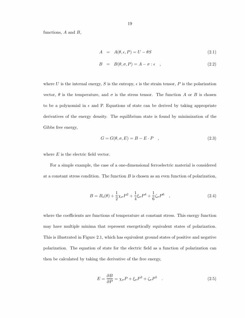
at a constant stress condition. The function B is chosen as an even function of polarization,
B = Bo(θ) +12χσP
2 +14ξσP
4 +16ζσP
6 , (2.4)
where the coefficients are functions of temperature at constant stress. This energy function
may have multiple minima that represent energetically equivalent states of polarization.
This is illustrated in Figure 2.1, which has equivalent ground states of positive and negative
polarization. The equation of state for the electric field as a function of polarization can
then be calculated by taking the derivative of the free energy,
E =∂B
∂P= χσP + ξσP 3 + ζσP 5 . (2.5)
20
Polarization
B −
Bo
Figure 2.1: Multiwell free energy vs. polarization for 1-D ferroelectric crystal.
The spontaneous polarization is found by minimizing G with respect to P at zero electric
field.
∂G
∂P=
∂B
∂P
∣∣∣∣E=0
= χσPs + ξσP 3s + ζσP 5
s = 0
∂2G
∂P 2=
∂E
∂P
∣∣∣∣E=0
= χσ + 3ξσP 3s + 5ζσP 5
s > 0 . (2.6)
The solutions of which are
Ps = 0 (nonpolar) and
P 2s = [−ξσ + (ξ2σ − 4χσζσ)1/2]/2ζσ (ferroelectric), (2.7)
where ζσ > 0, ξσ > 0, and χσ < 0 [9]. Given the values of the constants, the polarization
can be plotted as a function of electric field using Equation (2.5), as illustrated in Figure
2.2 as the smooth curve (a-d). There is an unstable region, (b-e), shown as a dashed curve.
The path bypasses the unstable region and instead jumps along the dotted line, (b-c), at

21
Electric Field
Pol
ariz
atio
n
Unstable Region
b
c
e
f a
d
Figure 2.2: Polarization vs. electric field calculated using the Landau-Ginsburg method fora 1-D ferroelectric crystal. The polarization follows the path (a-d), but the existence of anunstable region, shown as dashed line (b-e), cause the path to jump along the dotted line(b-c) at a critical electric field. On the reverse path, (e-f) is followed.
a critical electric field. On the reverse path, (d-a), the unstable region is bypassed by
following line (e-f). This curve closely resembles the polarization hysteresis loop observed
in ferroelectrics.
Similar analyses can be performed for more complicated systems, such as barium ti-
tanate, by considering the components of the polarization vector and the stress or strain
tensor. For example, the energy density function, A, is assumed
A(θ, ε, P ) = 12χijPiPj + 1
3ωijkPiPjPk + 14ξijklPiPjPkPl
+ 15ψijklmPiPjPkPlPm + 1
6ζijklmnPiPjPkPlPmPn
+ 12cijklεijεkl + aijkεijPk + 1
2qijklεijPkPl + · · · ,
(2.8)
where χij is the reciprocal dielectric susceptibility of the unpolarized crystal, cijkl is the
elastic stiffness tensor, aijk is the piezoelectric constant tensor, qijkl is the electrostrictive
constant tensor, and the coefficients are functions of temperature [5]. Such methodologies

22
have been very successful in the study of the behavior of ferroelectric crystals, ceramics,
and thin films including their phase transitions and the variation of the dielectric and
piezoelectric properties.
2.3 Finite Deformation Theory
A theoretical model of a ferroelectric single crystal has been developed by Shu and
Bhattacharya using the framework of finite deformation continuum mechanics [4]. The
model describes a system consisting of a ferroelectric crystal, Ω, as shown in Figure 2.3
in its reference (undeformed, nonpolar) configuration which is put in the presence of two
conductors, C1 and C2. The crystal is subject to a dead load with a traction, to, on its
boundary, ∂Ω, resulting in a nominal stress, σo, and an external electric field, Eo, resulting
from a charge, Q, on the conductors. The crystal undergoes a deformation, y(x), where x
is a point in the reference configuration and has a final polarization, p(y). The equilibrium
configurations of the crystal are studied by formulating an energy functional. The total
energy of the single crystal at temperature, θ, with an applied electric field and mechanical
load is formulated in the reference configuration and given by
E [y, p; θ] =∫
Ω
α|∇xP |2 +W (∇xy, P, θ) − (det∇xy)Eo · P − σo · ∇xy
dx
+12
∫IR3
|∇yφ|2dy , (2.9)
where P (x) = p(y(x)) is the expression of the polarization in the undeformed configuration
and the electric potential, φ, is determined by solving Maxwell’s equation,
∇y · (−∇yφ+ p) = ρ on IR3 , (2.10)

23
(Ω)
Ω
Figure 2.3: Continuum model of a ferroelectric crystal.
where ρ is the free-charge density and p = 0 outside of the crystal, and is subject to the
boundary conditions,
∇yφ = 0 on C1,
∫∂Ω
∂φ
∂ndS = 0, φ = 0 on C2, φ→ 0 as |y| → ∞ . (2.11)
The first term in Equation (2.9) involves the gradient of the polarization and thus
represents a domain wall energy. The second term is the free energy density, W , which
depends on the deformation gradient, polarization, and temperature. The third term is
the potential energy of the applied electric field, and the fourth is the potential energy of
the applied mechanical load. Note that (det∇xy) in the third term is necessary because
the polarization, p, is naturally defined in the deformed configuration. The second integral
is the electrostatic energy associated with the electric field generated by the spontaneous
polarization of the crystal itself. The equilibrium deformation and polarization can be found
by minimizing the total energy over all possible deformations, y, and polarizations, p.
The energy density,W , depends on the deformation gradient, F = ∇xy, the polarization,
P , and temperature, θ. It is frame-indifferent, i.e.,
W (QF,QP, θ) = W (F,P, θ) for all rotation matrices Q, (2.12)

24
satisfies material symmetry, and has multiple energy wells corresponding to the crystallo-
graphically equivalent configurations of the crystal. For tetragonal barium titanate, these
states correspond to the six spontaneously polarized 〈100〉 directions. Energy minimization
implies that the choice of equilibrium state will be determined by the applied mechanical
load and electric field.
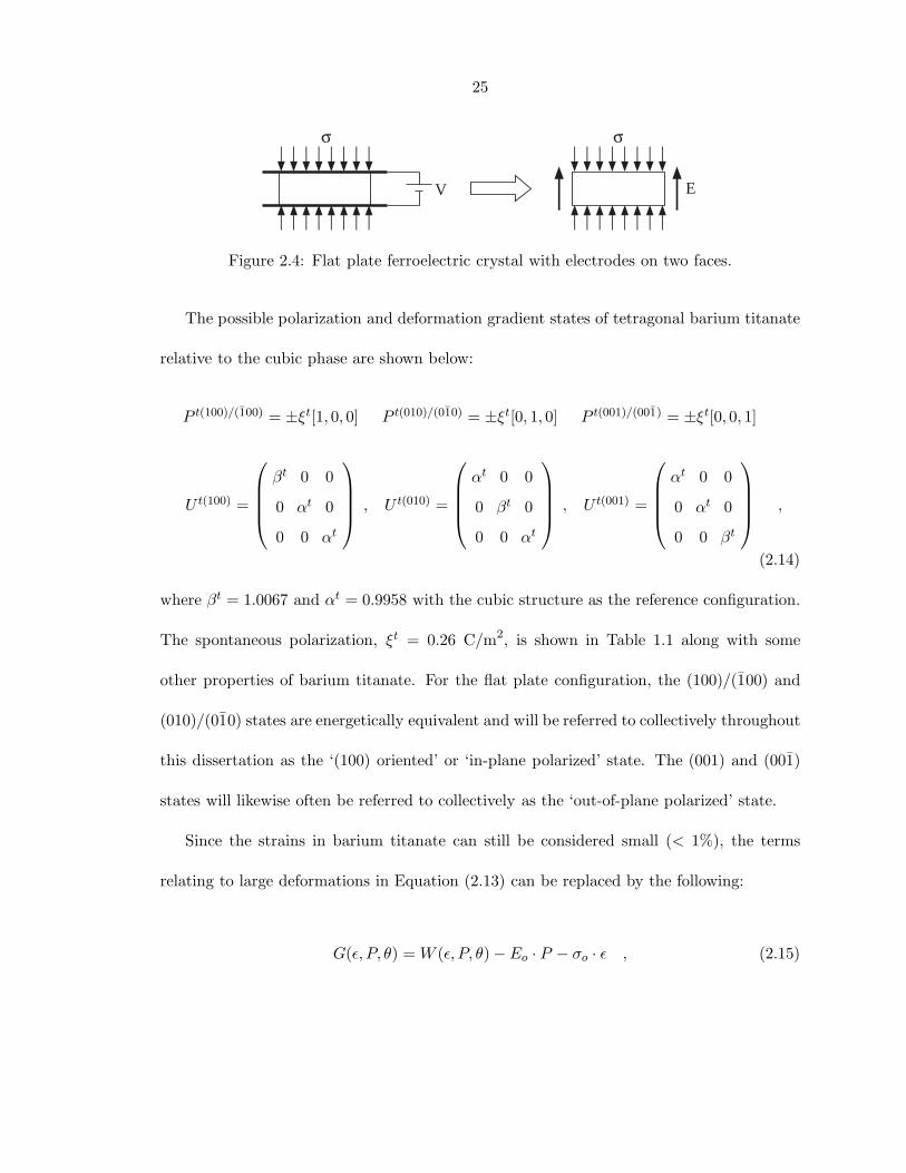
2.4 Flat Plate Configuration
For a flat plate configuration with electrodes on each face, shown in Figure 2.4, the
minimization problem can be simplified significantly. If the plate is thin and is bounded
by electrodes on the two major faces, the contribution of the electrostatic energy resulting
from the electric field generated by the spontaneous polarization of the crystal is limited
to the very narrow sides where no electrode is present. Thus for a very thin crystal, the
last integral in Equation (2.9) can be neglected. In addition, if the domain wall is assumed
to be a discontinuous boundary, the domain wall energy can be neglected, thus the first
term can be removed. This assumption is valid if the size of the crystal is much larger
than the domain wall. With these terms removed, the problem can then be reduced to the
minimization of the following energy density function:
G(F,P, θ) = W (F,P, θ) − (detF )Eo · P − σo · F . (2.13)
With this equation and knowledge of some material constants, the equilibrium configura-
tion for the crystal can be calculated as a function of stress, electric field, and temperature.
This calculation is examined for the case of a barium titanate single crystal whose pseudo-
cubic axis is oriented perpendicular to the plate.
25
V
σ
E
σ
Figure 2.4: Flat plate ferroelectric crystal with electrodes on two faces.
The possible polarization and deformation gradient states of tetragonal barium titanate
relative to the cubic phase are shown below:
P t(100)/(100) = ±ξt[1, 0, 0]
U t(100) =
βt 0 0
0 αt 0
0 0 αt
,
P t(010)/(010) = ±ξt[0, 1, 0]
U t(010) =
αt 0 0
0 βt 0
0 0 αt
,
P t(001)/(001) = ±ξt[0, 0, 1]
U t(001) =
αt 0 0
0 αt 0
0 0 βt
,
(2.14)
where βt = 1.0067 and αt = 0.9958 with the cubic structure as the reference configuration.
The spontaneous polarization, ξt = 0.26 C/m2, is shown in Table 1.1 along with some
other properties of barium titanate. For the flat plate configuration, the (100)/(100) and
(010)/(010) states are energetically equivalent and will be referred to collectively throughout
this dissertation as the ‘(100) oriented’ or ‘in-plane polarized’ state. The (001) and (001)
states will likewise often be referred to collectively as the ‘out-of-plane polarized’ state.
Since the strains in barium titanate can still be considered small (< 1%), the terms
relating to large deformations in Equation (2.13) can be replaced by the following:
G(ε, P, θ) = W (ε, P, θ) − Eo · P − σo · ε , (2.15)

26
where the spontaneous strain, ε, is related to the symmetric deformation gradient, U , by
ε = U − I , (2.16)
where I is the identity matrix and represents the reference configuration, i.e., the cubic state.
Thus the strain associated with a transition from an in-plane to out-of-plane polarized state
is about 1.09%. The stability boundary between the in-plane and out-of-plane states can
then be found by solving the equation
Gt(100)(ε, P, θ) −Gt(001)(ε, P, θ) = 0 . (2.17)
The standard transition temperature for the lower temperature orthorhombic phase can
be increased by suitable combinations of compressive stress and electric field, and thus it is
worthwhile to continue the analysis for this phase. The deformations and polarizations for
the orthorhombic phase are of the type
P o(011) = ξo[1, 1, 0] , Uo(011) =
βo 0 0
0 αo δo
0 δo αo
, (2.18)
where βo = 0.9975, αo = 0.9958 and δo = 0.00115 with the cubic structure as the reference
configuration. The polarization ξo = 0.21 C/m2 is also shown in Table 1.1. For complete-
ness, the form of the deformation and polarization for the rhombohedral phase are shown
as well.
P r(111) = ξr1, 1, 1, U r(111) =
αr δr δr
δr αr δr
δr δr αr
, (2.19)

27
where ξr = 0.19 C/m2, αr = 0.99999, δr = −0.00131.
The stability boundary between the in-plane and out-of-plane tetragonal and the or-
thorhombic phases can be found by solving the following equations, respectively,
Gt(100)(ε, P, θ) −Go(011)(ε, P, θ) = 0 (2.20)
Gt(001)(ε, P, θ) −Go(011)(ε, P, θ) = 0 , (2.21)
where
W t(ε, P, θ) −W o(ε, P, θ) ≈ −Lθc
(2.22)
and L = 2.38 × 10⁶ J/m3 is the latent heat of transition from orthorhombic to tetragonal
states at the standard transition temperature, θc = 5C.
The possible equilibrium configurations for a crystal of barium titanate cut in a flat plate
configuration with a 100 type orientation under combined electromechanical loading, are
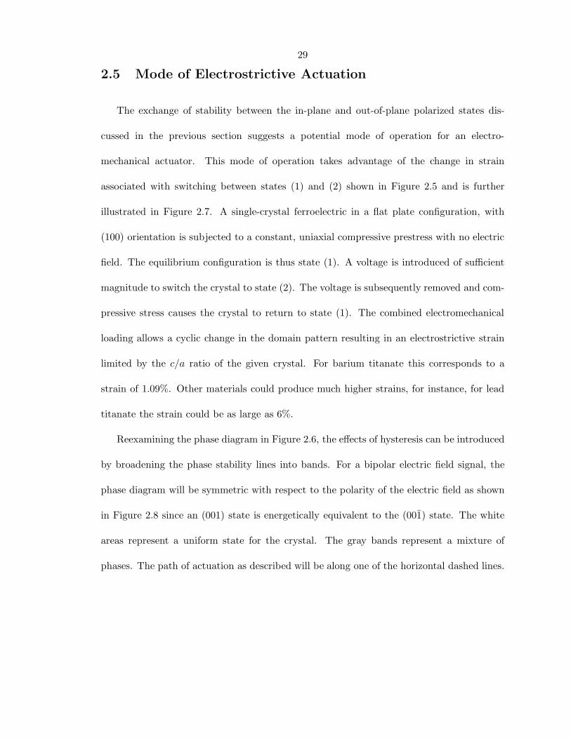
shown in Figure 2.5. The phase diagram in the compressive stress-electric field space for
the three configurations is shown in Figure 2.6. For this simplified analysis, the low order
effects such as piezoelectricity, pyroelectricity, and thermal expansion have been neglected.
The triple point is found to lie at a compressive stress of 384 MPa and electric field of 90.8
kV/cm. It is important to note that the configurations mentioned are equilibrium states.
The problem of switching between equilibrium states is kinetic in nature. No mention has
been made of the presence of multiple domains, the movement of which will contribute to
hysteresis.
28
o(1)
Eo(1)P(1)(1)
o(2)
Eo(2)P(2)(2)
o(3)
Eo(3)P(3)(3)
σ σ σ
Figure 2.5: Possible flat plate equilibrium configurations under compressive stress and elec-tric field loading.
0 20000 40000 60000 80000Electric Field (V/cm)
0
20
40
60
80
100
120
140
160
180
Com
pres
sive
Str
ess
(MP
a)
Tetragonal(in-plane)
(1)
Tetragonal(out-of-plane)
(2)
Orthorhombic(1)
Figure 2.6: Compressive stress-electric field phase diagram of barium titanate at roomtemperature. Triple point: σ = -384 MPa, E = 90.9 kV/cm.
29
2.5 Mode of Electrostrictive Actuation
The exchange of stability between the in-plane and out-of-plane polarized states dis-
cussed in the previous section suggests a potential mode of operation for an electro-
mechanical actuator. This mode of operation takes advantage of the change in strain
associated with switching between states (1) and (2) shown in Figure 2.5 and is further
illustrated in Figure 2.7. A single-crystal ferroelectric in a flat plate configuration, with
(100) orientation is subjected to a constant, uniaxial compressive prestress with no electric
field. The equilibrium configuration is thus state (1). A voltage is introduced of sufficient
magnitude to switch the crystal to state (2). The voltage is subsequently removed and com-
pressive stress causes the crystal to return to state (1). The combined electromechanical
loading allows a cyclic change in the domain pattern resulting in an electrostrictive strain
limited by the c/a ratio of the given crystal. For barium titanate this corresponds to a
strain of 1.09%. Other materials could produce much higher strains, for instance, for lead
titanate the strain could be as large as 6%.
Reexamining the phase diagram in Figure 2.6, the effects of hysteresis can be introduced
by broadening the phase stability lines into bands. For a bipolar electric field signal, the
phase diagram will be symmetric with respect to the polarity of the electric field as shown
in Figure 2.8 since an (001) state is energetically equivalent to the (001) state. The white
areas represent a uniform state for the crystal. The gray bands represent a mixture of
phases. The path of actuation as described will be along one of the horizontal dashed lines.

30
P P
0 V V
Figure 2.7: Mode of operation of an actuator based on combined electromechanical loadingof a ferroelectric single crystal.
Electric Field
σ
(100)
(001) (001)
Figure 2.8: Schematic bipolar phase diagram. The path for large strain actuation at con-stant compressive stress is represented by the dashed lines. Hysteresis is illustrated by thebroad gray bands which represent mixed-phase states.

31
References
[1] A. F. Devonshire, “Theory of barium titanate – Part I,” Phil. Mag. 40, pp. 1040–1063,
1949.
[2] A. F. Devonshire, “Theory of barium titanate – Part II,” Phil. Mag. 42(333), pp. 1065–
1079, 1951.
[3] A. F. Devonshire, “Theory of ferroelectrics,” Phil. Mag. Suppl. (Advances in Physics)
3(10), pp. 85–130, 1954.
[4] Y. C. Shu and K. Bhattacharya, “Domain patterns and macroscopic behavior of ferro-
electric materials,” Phil. Mag. A (submitted) .
[5] F. Jona and G. Shirane, Ferroelectric Crystals, Pergamon, New York, 1962. Reprint,
Dover, New York, 1993.
[6] B. A. Strukov and A. P. Levanyuk, Ferroelectric Phenomena in Crystals, Springer-
Verlag, New York, 1998.
[7] E. Fatuzzo and W. J. Merz, Ferroelectricity, Wiley, Interscience, New York, 1967.
[8] D. Damjanovic, “Ferroelectric, dielectric and piezoelectric properties of ferroelectric thin
films and ceramics,” Rep. Prog. Phys. 61, pp. 1267–1324, 1998.
[9] Y. Xu, Ferroelectric Materials, North-Holland, New York, 1991.

32
Chapter 3 EXPERIMENTAL METHOD
3.1 Overview
An experimental setup was designed and constructed to investigate large-strain elec-
trostriction in single-crystal ferroelectrics through combined electromechanical loading. The
system has the ability to apply a constant compressive load and variable electric field to a
ferroelectric crystal and allows accurate measurement of global strain and polarization. The
local behavior of domain motion can be observed under different loading conditions through
real time in situ observation of the domain patterns during the experiment. A schematic
diagram of the experimental setup is shown in Figure 3.1 and corresponding photographs
are shown in Figure 3.2.
3.2 Material
Experiments were performed on single-crystal barium titanate (BaTiO3). This material
was chosen because it has been widely studied and is available in single-crystal form. Barium
titanate is well suited to the experiments to be described because it is tetragonal at room
temperature, so is limited to 90 and 180 domain boundaries, and can be fairly easily
poled to single domain. The cut, poled, and polished crystals were obtained from two
outside sources, Superconix, Inc., Lake Elmo, Minnesota and Marketech International, Port
Townsend, Washington. Crystals were specified as 5 × 5 × 1 mm squares, either (100) or
(001) orientation, with both sides polished. A set of polydomain crystals were also obtained

33
!"#
$
"%&
"$'(
)
Figure 3.1: Schematic diagram of experimental setup and specimen dimensions.
from Superconix. These crystals were not poled prior to polishing and had a fine structure
of parallel domains. Poled crystals of (100) orientation were obtained from Marketech
International. (001) oriented, poled crystals were later obtained from Superconix.
3.3 Load Mechanism
The experimental setup was designed for constant load, variable electric field, quasi-
static experiments. Since the experiments were to be performed with a constant load, a
simple load mechanism was designed. The mechanism chosen was a lever system with dead-
weight loading. Diagrams of the loading mechanism are shown in Figure 3.3. Brass and
steel weights are hung on a hanger at the end of an aluminum beam. The force delivered
at the loading frame is four times the weight on the hanger plus the force due to the beam

34
Figure 3.2: Photographs of the experimental setup.

35
itself. Load is transmitted to the loading platens and specimen through a steel cross member
which is attached to the beam by a pin joint. Glass cylinders are used as platens and are
positioned on a steel loading frame. Details of the system are shown in Figures 3.4 and 3.5.
The glass cylinders, or optical flats, obtained from Edmund Industrial Optics are made
of fused silica and are polished to be 1/10λ optically flat on one surface. A transparent
material was chosen to allow direct, axial observation of the specimen during the test, as will
be described in more detail later. Since the experiments are performed at constant load, the
load frame compliance is not an issue. Experiments were performed in a low stress regime
with stresses from 0–5 MPa, corresponding to a weight of 0–28.9 N (0–6.5 lbs).
3.4 Strain Measurement
Strain in the specimen is measured by recording cross member displacement using a
Linear Variable Differential Transformer (LVDT). The LVDT is an electromagnetic dis-
placement sensor. It consists of two components, the coil and the core. The LVDT coil
is a set of three coils which are encased in a plastic and metal package. The package is a
cylinder with a hole in the middle in which the magnetic LVDT core is inserted. Movement
of the core about its zero position generates an electrical signal which is proportional to
the displacement. In the experiments, the maximum expected displacements are around
10 microns, which is within the range of a high resolution LVDT. The LVDT used for the
described experiments is a Schaevitz Sensors 025-MHR with a response of approximately
7.5 mV/µm.
The LVDT core is mounted on a beam, or lever, that is actuated from the center of the
load cross member, as seen in Figures 3.4 and 3.5. The beam pivots on a pin joint, thus the
core moves in the LVDT coil proportionally to the vertical movement of the cross member

36
Specimen andLoading platens
(20")50.8 cm
45.72 cm (18")
11.43 cm(4.5")
Hanger
Beam
Cross member
Loading Frame
Figure 3.3: Loading frame for constant load experiments on ferroelectric single crystals.

37
Figure 3.4: Closeup of experimental setup showing load cross member, specimen, loadingplatens, and LVDT actuation beam.

38
Figure 3.5: Photograph of experimental setup detailing displacement measurement andspecimen location.
but is insensitive to small rotations. Because of the dimensions of the beam, there is an
associated mechanical amplification of 2.5×. The LVDT coil is mounted to a miniature XY
stage to allow centering of the core in the LVDT and allow the signal to be zeroed prior to
the test. For very low frequency experiments, the flexibility of the actuator beam is not a
problem, but for higher frequency experiments, vibration of the actuator beam introduces
noise into the signal. This problem will be discussed in the final section of this chapter.
Calibration of the LVDT was performed by mounting the core on a separate translation
stage and moving it in the LVDT coil using a differential micrometer head with a resolution
of 0.5 µm.
3.5 Electrical System
3.5.1 Electrodes
Platinum electrodes are deposited directly on the polished surfaces of the crystals using
a sputter coater (Pelco SC-7). Issues concerning choice of electrode materials and electrode
design are discussed by Scott [1]. Prior to coating, the crystals are cleaned using isopropyl
and methyl alcohol. Afterwards, to avoid depositing metal on the sides of the specimen,

39
the sides are carefully masked with a narrow strip of cellophane tape. This masking tape
is removed following deposition. The crystal is sputtered for 35 sec. at 30 mA on each
side. This creates an electrode that is thin enough to see through under bright transmitted
illumination.
To connect the electrodes to the voltage source, platinum lines are deposited on the
optical flats mentioned in Section 3.3. Prior to coating the platinum lines, the optical flats
are cleaned using several solvents to remove any grease or oil on the surface. The solvents
used are methylene chloride, hexane, acetone, and methyl alcohol, in that order. Following
cleaning, the optical flats are masked using cellophane tape to generate the desired pattern.
The optical flats are sputtered for 25 sec. at 30 mA. Wires are bonded to the platinum lines
using conductive epoxy (Chemtronics CW-2400). The optical flats and crystal are then
stacked together and wired to the voltage source. The first optical flat is inserted into a
tube of thin acetate sheet. This tube prevents the stacked unit from slipping. The crystal
is placed in the middle of the optical flat, on top of the platinum line. To ensure good
conduction (contact) between the electrodes and platinum lines, small spots of conductive
carbon grease are placed at the corners of each electrode. The other optical flat is then
placed on top in the acetate tube. This stacked unit is then placed in the loading frame
and wired to the voltage source.
3.5.2 High-Voltage System
The high-voltage input signal is generated by a function generator connected to a high-
voltage power amplifier (Trek, Inc. Model 10/10B). This amplifier has a voltage range of
±10,000 V, a bandwidth of 4 kHz, and current limit of 10 mA. The amplifier takes a low
voltage input and generates a high-voltage output with a gain of 1000×. For the purposes

40
of these experiments, a function generator was used to generate the input signal. The
function generator used is a programmable digitally synthesized function generator from
Global Specialties, Inc. (Model 2003). Because the digital generator produces an 8 bit
signal there are small steps in the output signal. To smooth out these steps, a filter is used
between the function generator and high-voltage amplifier (Krohn-Hite Corp., model 3323).
The filter is set to a low pass (Butterworth) filter with a cutoff frequency of 10 times the
desired input frequency.
A connector box is used to connect the high-voltage amplifier to the specimen electrodes
and contains the Sawyer-Tower circuit used to generate the signal for polarization measure-
ment [2, 3, 4]. The circuit diagram of the high-voltage system and connector box is shown
in Figure 3.6. The Sawyer-Tower circuit is the most simple version of a charge amplifier.
The circuit consists of a capacitor, Co, with a large capacitance (10.46 µF) in series with
the crystal. Ideally, the charge on the capacitor will be the same as that on the crystal.
By measuring the voltage on the capacitor, the charge can be calculating using the familiar
equation
Qx = Qo = CoV , (3.1)
where V is the voltage drop across capacitor Co. Polarization is then calculated as the
charge per unit area of the electrode,
Px = Qx/A , (3.2)
where A is the area of the electrode. When measuring the voltage on the capacitor, it
is important to prevent the charge from leaking off into the measurement instrument too
quickly. For this reason, the voltage on the capacitor is measured through a voltage divider

41
FunctionGenerator
HighVoltageAmplifier
Co10.49 µF
Ro100 MΩ
OscilloscopeRI = 1 MΩ
Specimen (Cx)
Figure 3.6: Block diagram of high-voltage system.
circuit with a 100 MΩ resistor (Ro) in series with the oscilloscope. The oscilloscope has
a 1 MΩ input impedance, so the measured voltage is 1/101 of the actual voltage. Since
the crystal’s initial polarization state is usually not zero, there is a DC component to the
polarization signal which decays very slowly over the course of the 200 sec. experiment.
This decay follows an exponential law and can be easily subtracted from the signal. An
example of charge data before and after the exponential shift is shown in Figure 3.7.
3.6 Polarized-Light Microscopy
A long working distance, polarizing microscope was designed to make observations of
the crystal during the experiment. The system uses transmitted, white-light illumination to
visualize domains and domain boundaries in the ferroelectric crystal. The use of transparent
loading platens and thin sputtered electrodes allows the light to pass through the electrodes
along the loading axis to allow direct observation of the crystal during the experiment. The
principles of birefringence contrast that allow optical visualization of domains are described

42
0 50 100 150 200−4
0
4
8
12
time (sec.)
char
ge (
C)
Unshifted
0 50 100 150 200−8
−4
0
4
8
time (sec.)
char
ge (
C)
Shifted
Figure 3.7: Charge signal before and after removing the exponential decay.
in this section along with a detailed description of the microscope system.
3.6.1 Birefringence Contrast
A very thorough reference for polarized-light microscopy with ferroelectric materials
can be found in the work of Schmid [5]. The most important effect for obtaining contrast
between 90 domains is the spontaneous linear birefringence of the material. When a barium
titanate crystal of (001) orientation is placed between crossed polarizers and illuminated in
transmission, as shown in Figure 3.8, the field will remain dark since the material is optically
isotropic in that direction. When an in-plane polarized domain is introduced, however, a
rotation of the polarization direction occurs, resulting in a birefringence contrast which is
a function of the in-plane polarized domain thickness, d. The intensity, I, is governed by
the following equation:
I = I sin2 2θ · sin2(πd/λ)(n′′ − n′) , (3.3)

43
Linear Polarizer
Linear Polarizer
Io
I
d
0 10 20 30 40 500
0.2
0.4
0.6
0.8
1
Domain thickness (µm)
Inte
nsity
(I/I
o)
(a) (b)
Figure 3.8: (a) Generation of birefringence contrast in tetragonal barium titanate and (b)intensity vs. domain thickness, d, with 632 nm illumination.
where I is the incident intensity, n′ is the ordinary refractive index, n′′ is the extraordinary
refractive index, θ is the angle between the plane of vibration of the polarizer and the
vibration direction of n′′, λ is the wavelength of the light, d is the thickness of the in-
plane polarized domain, and n′′ − n′ is the birefringence [5]. The value of birefringence
for barium titanate at room temperature is −0.073 (see Table 1.1). The intensity as a
function of domain thickness for barium titanate with θ = 45 and λ = 632 nm illumination
is shown in Figure 3.8. When white-light illumination is used, the recorded intensity will
be determined by the spectrum of the illumination source and the spectral response of the
imaging sensor.
3.6.2 Illumination and Charge Coupled Device (CCD) Sensor
For the current experiments, the crystal is illuminated in transmission using white light
from a fiber optic illuminator (Dolan-Jenner 170-D). This illuminator uses a 150 W quartz
halogen lamp. The spectrum of this type of lamp (Ii (λ)) is shown in Figure 3.9.

44
0.2 0.4 0.6 0.8 10
0.2
0.4
0.6
0.8
1
Wavelength (µm)
Rel
ativ
e in
tens
ity
Figure 3.9: Spectrum of the quartz halogen fiber optic illuminator (EKE 21 V, 150 W lamp)(data courtesy of Dolan-Jenner Industries, Inc.).
The camera used for the experiments is a monochrome Charge Coupled Device (CCD)
video camera (Sony XC-75). When doing polarized microscopy observations using white-
light illumination, the recorded intensity of the image will be an integrated value over the
visible spectrum, subject to the spectrum of illumination and the spectral responsivity of the
CCD sensor. The spectral responsivity curves of the CCD and the attached infrared (IR)
filter are shown in Figure 3.10. The combined response of the two components is roughly
parabolic and centered at about 500 nm. A predicted relative intensity curve (normalized)
as a function of in-plane polarized domain thickness is shown in Figure 3.11. Note that the
response is quite different from that shown in Figure 3.8 (b). This is because the intensity
is integrated over the wavelengths for which the camera is sensitive. The predicted relative

45
0.4 0.5 0.6 0.7 0.8 0.9 10
0.2
0.4
0.6
0.8
1
Wavelength (µm)
Rel
ativ
e re
spon
se
CCD IR filterCombined
Figure 3.10: Spectral responsivity of Sony XC-75 CCD camera (data courtesy of SonyCorp.)
intensity curve in Figure 3.11 is calculated using the following equation:
R (d) =∫ ∞
0α (λ) Ii (λ) I (λ, d) dλ , (3.4)
where R is the recorded intensity from the CCD camera, α is the responsivity of the CCD
camera (Figure 3.10), Ii is the spectrum of the illuminator (Figure 3.9) and I is the intensity
from Equation (3.3).
3.6.3 Mechanical System
The long working distance microscope used for the experiments has quite a simple de-
sign. A schematic diagram of the microscope is shown in Figure 3.12. A list of components
of the microscope is provided in Table 3.1. The microscope has only two optical compo-

46
0 10 20 30 40 500
0.2
0.4
0.6
0.8
1
Domain thickness (µm)
Rel
ativ
e in
tens
ity
Figure 3.11: Predicted relative intensity vs. 90 domain thickness.
nents, an objective and a linear polarizing filter. The objective used is a 10× toolmaker’s
objective from Nikon (model 18298) with a finite tube length of 210 mm. The image plane
must be placed at an optical distance of 210 mm to avoid any chromatic distortions. Thus,
a specially designed extension tube is used to link the C-mount CCD camera to the objec-
tive. The dimensions of the extension tube are shown in Figure 3.13. The extension tube
is constructed of aluminum with the inside surface coated with flat black spray paint to
eliminate any internal reflections or halo effect. The polarizer is mounted immediately in
front of the objective using an aluminum sleeve which is secured using a nylon thumb screw.
An additional polarizer is mounted under the specimen using a rotatable optical mount.
A rack-and-pinion focusing stage with both coarse and fine focus is used to focus the
microscope by moving it vertically. The extension tube is attached to the focusing unit
using a ring clamp. The focusing unit is supported with a 1 in. diameter stainless steel post

47
!"
#$%&
'"
'(
)*"
Figure 3.12: Schematic diagram of long working distance polarizing microscope.
3.175cm(1.250")
External Thread1-32 TPI(C-mount)
Internal ThreadM26-0.75 mm
2.062cm(0.812")
19.66cm(7.740")
19.248cm(7.578")1.02cm
(0.400")
Figure 3.13: Dimensions of extension tube for microscope for use with Nikon 210 mm tubelength objectives and C-mount camera.
and attached to an XY translation stage for precise positioning of the microscope over the
specimen.

48
Table 3.1: List of microscope components.
Description Manufacturer Model10×, Long working distance
objective, 210 mm tube length, Nikon 1829849.5 mm working distance
Rack and pinion focusing mount Edmund Industrial Optics 54-794with course/fine movement
25 mm linear polarizing filter Edmund Industrial Optics 43-78650.8 mm mounted iris diaphragm Edmund Industrial Optics 53-915
Quartz halogen fiber optic Dolan-Jenner Industries 170Dilluminator (EKE 21 V, 150 W)
Steel XY Translation Stage Melles-Griot 07 CXY 0041/2 in. CCD video camera Sony Corp. XC-75
3.6.4 Video System
A CCD (Charge Coupled Device) video camera was used for imaging the domain struc-
ture of the ferroelectric crystal during the experiment. The camera used is a Sony XC-75
monochrome CCD camera. This camera has a 1/2 in. CCD with 768 × 494 pixels. The
camera generates 30 frames per second of interlaced video using the RS-170 signal stan-
dard. The camera outputs an analog signal through a BNC cable which is compatible with
standard video hardware and can be digitized using a computer-based card.
The camera generates an interlaced image, meaning that each frame is generated by two
scans, or fields, each every 1/60 sec. The first scan reads the ‘odd’ lines, while the second
scan reads the ‘even’ lines. These two fields are then interlaced to produce a complete
image every 1/30 sec. This interlaced system is used so that the camera is compatible with
standard video hardware, such as televisions or VCRs. One adverse effect of interlaced video
is that if the object moves very quickly, the two fields may appear to be shifted relative to
each other, as shown in Figure 3.14. For more information on video camera fundamentals,
see Inoue [6].

49
(a) (b)
Figure 3.14: Sample captured images (a) with a steady camera and (b) a shaking cameraillustrating the distortion caused by interlaced fields.
Images from the camera are captured using a computer-based digital frame grabber
card. The card used is an Epix PIXCI SV-4 from Epix Inc., Buffalo Grove, Illinois. The
card is PCI based and is able to capture images from a standard video camera at up to
30 frames of interlaced video per second. The card digitizes the analog video signal and
saves the image information into system memory at up to 752 × 480 pixels and 8 bits per
pixel. Indexed images can be saved with each pixel assigned a gray level or brightness
from 0 (black) to 255 (white). At this resolution the image pixels are rectangular with a
4/3 aspect ratio, so images are generally captured at a resolution of 644 × 480 pixels for a
one-to-one aspect ratio. The card also features general purpose digital outputs and inputs
for use in triggering.
3.7 Instrumentation
The experiment is controlled by a computer using digital outputs from the video frame
grabber card. A flow chart showing the instrumentation control path used in the experi-
ments is shown in Figure 3.15. A list of instruments used is shown in Table 3.2. At the
beginning of the experiment, a program is run and the timing parameters are input, e.g.,

50
duration of the experiment, initial capture time, and rate at which the video should be
captured. The frame grabber is equipped with four general-purpose digital outputs used
for triggering other instruments. One of these outputs, shown as Trigger 1 in the figure, is
used to trigger the function generator and the digital oscilloscope used for recording data.
Initial experiments were performed using a Nicolet Pro 440 digital oscilloscope to capture
21,000 data points per channel. Later experiments were performed using a Nicolet Integra
40 oscilloscope capturing 50,000 data points per channel. A second general-purpose output,
shown as Trigger 2, triggers a second oscilloscope and indicates when the frame grabber
begins capturing images. The second oscilloscope is used only for diagnostic purposes.
The function generator signal passes through a low pass filter to smooth the 8 bit
digitally synthesized signal. This signal is used as an input to the high-voltage amplifier
which outputs a proportional signal with a gain of 1000. The amplifier voltage monitor and
current monitor output signals of 1 V/kV and 1 V/mA, respectively, are recorded on the
first digital oscilloscope. The output from the high-voltage amplifier is used as the voltage
input to the crystal specimen. As mentioned earlier, the strain is measured using an LVDT.
The output from the LVDT signal conditioner passes through a differential amplifier with
1000 Hz low pass filter to the digital oscilloscopes. For some cases, the LVDT signal was
also filtered using a 40 Hz low pass filter (Krohn-Hite Model 3323) to remove the 100 Hz
vibration noise. Output from the Sawyer-Tower circuit is also recorded.
During the fifth cycle of the experiment the frame grabber begins recording images from
the CCD camera. At the same time, the frame grabber generates a signal to the second
digital oscilloscope indicating the time that recording starts. The images are captured at a
prescribed capture rate, usually 30 frames per second.

51
Table 3.2: List of instruments.
Description Manufacturer ModelHigh-voltage amplifier, ±10 kV, Trek, Inc. 10/10B
10 mA, 4 kHz bandwidthDigital synthesized Global Specialties 2003function generatorDigital oscilloscope Nicolet Instrument Pro 440,
4 channels, 12 bit digitizer Technologies, Inc. Integra 40Dual channel digital oscilloscope Nicolet Model 4094
Differential amplifier, Preston Instruments 8300 XWBDC–100 kHz bandwidth
Dual channel active tunablelow pass/high pass filter, Krohn-Hite Corp. 3323
0.01 Hz–100 kHz bandwidthHigh resolution LVDT Schaevitz Sensors 025-MHR
PCI frame grabber card Epix, Inc. PIXCI SV-4800 MHz Pentium III PC Dell Computer Corp. Dimension
with 256 MB RAM XPS T800r
3.8 Limitations
Because of the large masses involved in the loading mechanism, the system is only
suitable for low frequency or quasi-static experiments. At higher frequencies, the inertial
effects will cause the assumption of constant stress to be invalid. Additional limitations are
introduced by the vibrational modes of the LVDT actuator beam. A vibration experiment
was performed to find the vibrational modes of the actuator beam. The setup was assembled
with a dummy specimen, loading platens and cross member with the loading beam removed.
A free vibration was induced by manually striking the optical table on which the setup is
assembled and recording the LVDT signal. The FFT (Fast Fourier Transform) of the LVDT
signal is shown in Figure 3.16. The strongest mode of vibration is at about 97 Hz. The
predicted first mode of vibration is about 140 Hz if the actuator beam is assumed to be a
cantilever fixed at the pivot point which would be somewhat stiffer than the actual beam.
The weaker mode at about 27 Hz is probably a secondary vibration of other components

52
Sawyer-Tower Circuit
AmplifierSignalConditioner
Low PassFilter
FunctionGenerator
High VoltageAmplifer
LVDT
VoltageMonitor
CCDCamera
Crystal
DigitalOscilloscope 1
Frame GrabberBoard
DigitalOscilloscope 2
Trigger 2
Trigger 1
CurrentMonitor
Computer
Figure 3.15: Flow chart of instrumentation system.
of the system, such as the optical table. Noise caused by 97 Hz vibration is sometimes
present in the strain signals, but for experiments at input frequencies of less than 1 Hz, the
vibration noise can be filtered out either digitally after the experiment or by using a low
pass filter on the LVDT signal during the experiment. For experiments with input signals
of around 5 Hz or greater, the vibration noise can not be separated from the actual strain
signal.
The major limitations of the polarizing microscope are its lateral resolution and depth
of field. In its current state, the polarizing microscope has a pixel resolution of about one
micron, thus features of only about three–five microns can be distinguished, at best. In
some cases, domain structures may be smaller than this level and can not be imaged. The
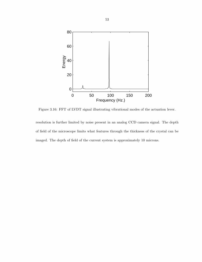
53
0 50 100 150 200
0
20
40
60
80
Frequency (Hz.)
Ene
rgy
Figure 3.16: FFT of LVDT signal illustrating vibrational modes of the actuation lever.
resolution is further limited by noise present in an analog CCD camera signal. The depth
of field of the microscope limits what features through the thickness of the crystal can be
imaged. The depth of field of the current system is approximately 10 microns.

54
References
[1] J. F. Scott, “The physics of ferroelectric ceramic thin films for memory applications,”
Ferroelectrics Review 1, pp. 1–129, 1998.
[2] Y. Xu, Ferroelectric Materials, North-Holland, New York, 1991.
[3] C. B. Sawyer and C. H. Tower, “Rochelle salt as a dielectric,” Phys. Rev. 35, pp. 269–
273, 1930. [see Jaffe, Piezoelectric Ceramics, Acad. Press, 1971].
[4] B. Jaffe, W. R. Cook, and H. Jaffe, Piezoelectric Ceramics, Academic Press, New York,
1971.
[5] H. Schmid, “Polarized light microscopy (PLM) of ferroelectric and ferroelastic domains
in transmitted and reflected light,” in Ferroelectric Ceramics: Tutorial reviews, theory,
processing, and applications, N. Setter and E. L. Colla, eds., pp. 107–126, Monte Verita,
Zurich, 1993.
[6] S. Inoue, Video Microscopy, Plenum Press, New York, 1986.

55
Chapter 4 RESULTS
4.1 Overview
Experiments have been performed to investigate the stress dependence of the elec-
trostrictive response of barium titanate single crystals. A set of experiments was performed
on initially single domain (100) and (001) oriented crystals at different levels of compressive
stress. Actuation strain and coercive field as a function of stress are reported. A limited in-
vestigation of the frequency dependence of the response is presented with input frequencies
of 0.05 to 1.0 Hz. Video observations are presented and correlated to the measured strain
and polarization. Finally, observations of cracking and damage mechanisms are discussed.
4.2 Global Measurements
During the experiment, a low frequency voltage signal is generated and the strain and
polarization are measured. Figure 4.1 shows strain data from a typical experiment with an
input signal frequency of 0.05 Hz. In Figure 4.1 (a), the electric field input signal is shown
as the solid curve and the strain signal is shown as the dashed curve. As the electric field
increases, the strain suddenly increases and then levels off. As the electric field is decreased,
the strain decreases and then increases again as the electric field becomes negative. Thus,
there are two strain cycles for each cycle of electric field. This is shown more clearly in
Figure 4.1 (b), where strain is plotted as a function of the electric field with the first
cycle absent. This is an example of the ‘butterfly’ hysteresis loop for strain [1, p. 148].

56
Note that the strain is approximately symmetric with respect to electric field. Also note
that the strain does not reach its minimum level at zero electric field. A negative bias is
required to ‘kick’ the strain down to its minimum level before it increases again. Because
of the symmetric behavior of the strain with respect to polarity of the electric field, the
deformation is characterized as electrostrictive in the general sense described in Chapter 2.
The corresponding plots of polarization data are shown in Figures 4.2 (a) and (b). Like
the strain signal, as the electric field increases, there is a sudden increase in polarization, fol-
lowed by a leveling off at a maximum level of about 0.28 C/m2. The polarization decreases
as electric field decreases and levels off at a negative value. Thus there is one polarization
cycle for each cycle of electric field. When plotted as a function of electric field, the polar-
ization displays a familiar hysteresis loop. The difference in the character of the strain and
polarization hysteresis is explained by the fact that for tetragonal barium titanate, there is
no strain change associated with a 180 reversal of polarization.
4.2.1 (100) Oriented Crystal
A series of strain-electric field trajectories is shown in Figure 4.3 at five values of com-
pressive stress ranging from 0 to 1.78 MPa. The data shown are for an initially (100)
oriented crystal and are taken from the fifth cycle of each experiment, when the response
has reached a steady state. The input signal has a frequency of 0.05 Hz with an amplitude
of ±10,000 V/cm. The first plot has a compressive stress of approximately zero (there is a
negligible, yet small stress present due to the measurement method). In this case, the total
electrostrictive strain is quite low (less than 0.1%). When the stress is increased to just
0.36 MPa, the maximum strain increases to more that 0.3%. While this stress is quite low,
it is consistent with the observations of Li et al. who noted introduction of 90 domains in

57
barium titanate crystals at stresses of just 0.22 MPa [2]. With subsequent increase in com-
pressive stress, there is an increase in the maximum strain up to about 0.8% at 1.78 MPa.
In addition, at larger stresses there is a broadening of the butterfly hysteresis loops.
Figure 4.4 shows a series of polarization-electric field trajectories for the same cases. For
the zero stress case, the hysteresis curve has very sharp corners as is usually observed for
single-crystal ferroelectrics [1]. The spontaneous polarization at low stress is measured to
be about 0.27 C/m2 which is in agreement with the published values of 0.25 and 0.26 C/m2
for barium titanate [3][1, p. 115]. As the stress is increased, the corners become blunted
and the area of the hysteresis loops become larger. This is consistent with the increased
hysteresis in the strain plots. Strain is plotted as a function of polarization in Figure 4.5.
Each of the curves show a very flat region at low levels of polarization and a very sudden
rise at a critical value of polarization which decreases with increasing stress. Hysteresis is
present at low stresses but disappears at higher levels of stress.
4.2.2 (001) Oriented Crystals
Strain-electric field trajectories for six experiments with an initially (001) oriented crys-
tal are shown in Figure 4.6 over a wider range of stress than the previous set. A 0.05 Hz
input signal with an amplitude of ±7,500 V/cm is used for these cases. At zero stress, the
magnitude of the actuation strain is again very low, appearing as a nearly horizontal line
in the plot. As the stress is increased, the magnitude of the actuation strain increases to
a maximum of about 0.9% at a stress of 2.14 MPa. As the stress is further increased, the
actuation strain decreases and the hysteresis loops broaden as the applied field is unable to
overcome the applied stress. The trend of increasing and then decreasing actuation strain
with increasing stress is quite similar to that observed by Lynch in preloaded PLZT ceramic

58
materials [4].
The polarization-electric field behavior is somewhat different than the previous case.
At low stress the polarization has a very rectangular hysteresis loop with sharp corners, as
expected [1]. Spontaneous polarization at low stress for this crystal is measured to be about
0.28 C/m2. At higher levels of stress, up to about 1.07 MPa, the corners are somewhat
smoothed out like in the previous case, but to a lesser extent. At higher stresses, however,
the behavior is quite different. A secondary hysteresis is introduced at a high offset level
of polarization, which will be discussed in the next paragraph. When strain is plotted as
a function of polarization in Figure 4.8, there is little visible hysteresis. As in the previous
case, there is a flat region at low levels of polarization and a sudden, almost linear rise in
strain at a critical polarization, which varies from about 0.28 C/m2 at a compressive stress
of 0.36 MPa to about 0.19 C/m2 at a compressive stress of 3.92 MPa.
There is a distinct difference in the polarization hysteresis loops for the initially (100)
and (001) oriented crystals, shown in Figures 4.4 and 4.7, respectively. The (100) crystal
exhibits a smooth transition, while the (001) crystal exhibits an unusual secondary hysteresis
at high levels of polarization. The appearance of the hysteresis loops is very similar to the
“triple hysteresis loops” that have been observed in orthorhombic barium titanate near
the orthorhombic-tetragonal phase transition temperature [5]. This similarity suggests that
a first-order phase transition may be occurring in this case. The linear portions of the
secondary hysteresis loops were extrapolated to the P -axis to determine the ‘primary’ and
‘secondary’ spontaneous polarizations (Ps1 and Ps2, respectively), as shown in Figure 4.9.
The primary spontaneous polarization is found to be about 0.26 C/m2, in-line with the
low stress value of spontaneous polarization mentioned earlier. The secondary spontaneous
polarization is found to be about 0.19 C/m2, which is quite close to the published value of

59
spontaneous polarization of orthorhombic barium titanate of 0.21 C/m2 [3]. Based on the
simple phase equilibrium calculation shown in Chapter 2, the orthorhombic phase should
not appear at such low stresses and electric fields. Further study with X-ray analysis would
be required to determine whether a phase transition is occurring and what the intermediate
phase is.
4.2.3 Actuation Performance
The overall actuation performance of several crystals is compared in Figure 4.10 where
steady state actuation strain is plotted as a function of compressive stress. The actuation
strain is defined as the difference between the maximum and minimum strain for a given
half cycle. The values are calculated in the fifth input cycle after the response has reached
a steady state, with two values plotted for each experiment: for the electric field rise and
electric field drop. Data for an initially (100) and two initially (001) oriented crystals are
shown. There is a clear increase in actuation strain with increasing stress in each case with
the maximum recorded value of 0.9%.
The data for the (100) oriented crystal discussed in Section 4.2.1 are plotted as the
triangles (). The actuation strain increases monotonically with stress and is fitted with a
parabolic curve. The data for the (001) oriented crystal discussed in Section 4.2.2 are plotted
as the × symbol. For this case the actuation strain again increases smoothly with increasing
stress closely following the data for the (100) crystal. The maximum strain is reached at
2.14 MPa after which the actuation strain begins to fall as stress is further increased. A
second set of data for a (001) oriented crystal is shown using the open circle symbol (©).
For two levels of stress (0.36 MPa and 1.07 MPa), data for multiple experiments on the
same crystal are shown. The actuation strains for this crystal are lower than the previous

60
two and the data is more scattered but follows the same overall trend. The variation of
performance between crystals may be due to variations in the quality of the material, for
instance, the presence of defects or impurities.
Coercive field, defined as the field required to reduce the polarization to zero (see Sec-
tion 1.2.1), is shown as a function of compressive stress in Figure 4.11. This data is also
calculated in the fifth cycle of each experiment and two values are reported for each case.
In contrast to the actuation strain, the coercive field is found to be relatively insensitive
to stress. For the (001) crystal discussed in Section 4.2.2, the coercive field is essentially
constant. Repeatability between crystals is fairly good with all points falling between 350
and 550 V/cm.
The rise and fall of the actuation strain with increasing compressive stress can be ex-
plained by reexamining the modified phase diagram presented in Figure 2.8 in Section 2.5.
Along the path of actuation (the horizontal dashed lines) the boundary of the gray shaded
regions can be seen as the saturation point at which the crystal goes from a mixed-phase
state to a uniform state. At moderate stresses, the path goes through all three uniform
states. At high stresses the path does not emerge from the mixed state region for a con-
stant range of electric field.
From the experimental strain data, the point of saturation to the (001) or (001) states
can be determined by defining a critical magnitude of the slope of the strain-electric field
curve,(
dεdE
).
(dεdE
)vs. electric field is plotted in Figure 4.12 for a (100) oriented crystal at
1.07 MPa compressive stress. The saturation electric field is defined for the increasing region
of the strain-electric field curve (increasing electric field and strain), where the magnitude of
(dεdE
)drops below 0.01%/kV/cm. This is labeled as point 1 in the plot for both negative and
positive electric field. The ‘desaturation’ point is defined for the return path (decreasing

61
electric field and strain), where the saturated strain begins to decrease. It is defined as
the electric field at which the magnitude of(
dεdE
)exceeds 0.01%/kV/cm and is labeled as
point 2 for both positive and negative electric field.
Comparison with the theoretically predicted phase diagram can be made by plotting
the saturation and desaturation points in the compressive stress-electric field space. In
Figure 4.13, data are plotted for (100) and (001) oriented crystals. The data were obtained
during the fifth cycle of each experiment. The shaded symbols are the saturation values
and the open symbols are the desaturation values. Values are plotted for experiments with
compressive stresses of up to 2.14 MPa. For larger stresses, the saturation and desaturation
points could not be determined. Lines have been fitted to the combined sets of data for the
two crystals and extrapolated to electric fields of ±8 kV/cm. The predicted equilibrium
phase boundaries are plotted as the dashed lines. The experimental paths for four levels
of stress are plotted as the horizontal gray lines. The cycle starts at zero electric field and
travels to the right along the horizontal line. The crystal reaches saturation when it passes
through the saturation line. The maximum electric field is reached at point × and then
decreases. The crystal loses saturation as it passes the desaturation line traveling left on
the horizontal path.
The data for the two crystals fall very close together and are symmetric with respect
to electric field polarity. The slopes of the saturation lines, however, are much lower than
the slopes of the predicted phase boundary lines. The extrapolated saturation lines can
be used to estimate the required electric field range for large strain performance at higher
stress; however, it is difficult to assess a saturation bounds for the in-plane polarized (100)
state. For an electric field range of ±7.5 kV/cm, the extrapolated saturation lines predict
that experiments for stress levels of about 3 MPa and above will not reach saturation

62
lines. This is consistent with the observed decrease in actuation strain at higher stresses.
The difference between the observed saturation behavior and the predicted equilibrium
boundaries are explained by local pinning of the (100) domains. This may be due to high
localized stresses due to friction at the surfaces, defects, and surface imperfections.
The mechanical work per unit volume for each actuation stroke is plotted as a function of
compressive stress in Figure 4.14. The values are calculated for each experiment during the
fifth cycle by multiplying the magnitude of the compressive stress by the actuation strain.
The maximum work per unit volume is about 27,000 J/m3 at 5 MPa compressive stress.
The upper bound of the work per unit volume is plotted as the dashed line calculated using
an actuation strain of 1.1%. The ratio of the measured work per volume to the predicted
upper bound is plotted on the lower axes. The ratio starts below 20% for low stresses and
increases to over 80% at around 2 MPa compressive stress and then decreases, following the
trend of the actuation strain shown in Figure 4.10. At higher stresses the experimental work
per unit volume is limited by the input electric field range. The predicted value for high
strain ferroelectrics, shown in Figure 1.1 in Chapter 1, was about 106 J/m3. To reach this
level of work per unit volume would require a compressive stress of about 100 MPa. Based
on the extrapolated linear saturation line in Figure 4.13, this would require an electric field
range of about ±250 kV/cm, which falls within the range of the reported breakdown field
of the material [3, p. 350]. In any case, this may be impractical for bulk crystals because
it would require extremely high voltages of ±25 kV for 1 mm thick crystals. However, this
level of electric field would be more easily obtainable for thin film materials.

63
4.3 Frequency Response
Frequency dependence of the strain response at different stresses is of interest to deter-
mine the suitability of the mode of actuation to different applications. The experimental
setup used is only suitable for pseudo-static, or very low frequency experiments, however,
a limited investigation is possible. Figure 4.15 shows the strain-electric field trajectories at
several different frequencies and compressive stresses of 1.07 and 2.14 MPa. The input sig-
nal frequencies shown are 0.05, 0.1, 0.5, and 1.0 Hz. Higher frequency tests are not possible
due to induced mechanical vibrations that appear within the frequency range of the strain
signal (see Section 3.8). For the 1.07 MPa experiments, the maximum actuation strain for
the tests increases with increasing input frequency. For the higher stress cases (2.14 MPa),
the behavior is insensitive to frequency within the range tested.
4.4 Polarized-Light Microscopy Observations
Observations are made of the crystal domain patterns during the experiment using a
polarizing video microscope. Figure 4.16 shows a sequence of five images of domain patterns.
These images are chosen from a series of images taken over the course of one cycle on an
initially (001) oriented crystal at a compressive stress of 1.07 MPa. The field of view is
about 0.65 × 0.5 mm and is located at the center of a crystal of about 5 × 5 mm lateral
dimensions. As explained in Section 3.6, the crystal is imaged through the electrodes with
transmitted illumination along the loading axis. The images in the figure are numbered
in sequence corresponding to the labeled plots of strain and polarization vs. electric field.
The initial image is taken at an electric field of −6, 400 V/cm. At this stage the crystal
is at nearly its maximum level of strain and minimum level of polarization. The image is

64
nearly black, indicating that the crystal is completely [001] polarized. In the second image
(E = −180 V/cm) a bright band of the in-plane polarized domains has entered the field
of view. The strain has decreased by about 0.4% and polarization has begun to increase.
The bright band is broken into two regions by a faint horizontal boundary, which is a
surface feature present in all of the images. In the third image, as the electric field further
increases to the level of the coercive field (E = 500 V/cm) the image is completely bright
with in-plane polarized domains throughout the field of view. A series of horizontal bands
of 50–100 µm in width are visible that divide the bright region. The boundaries between
the bands may be 180 or 90 domain boundaries between the in-plane variants. At this
point the strain has reduced to its minimum level and the polarization is zero. In the fourth
image (E = 1170 V/cm), the in-plane polarized domains have begun to disappear from the
field of view as the strain begins to increase and the polarization begins to level off. By the
time the electric field has reached 5,600 V/cm in the fifth image, the strain and polarization
have nearly reached their maximum levels and the image is again completely black.
The sequence of images detail a level of large scale inhomogeneity of the deformation
of the crystal. The large uniform out-of-plane polarized region in the first image is broken
up by bands of in-plane polarized domains that sweep through the field of view in one
direction. The fact that the reduction in the strain coincides with an appearance of the
in-plane polarized domains and that the rise of the strain coincides with their disappearance
supports the hypothesis that 90 domain motion and switching are responsible for the large-
strain electrostrictive behavior. This useful information is qualitative in nature and relates
to the local behavior. Since the images represent only a small area of the crystal (∼1%) and
the deformation is apparently very inhomogeneous, it is questionable whether a quantitative
correlation can be drawn to the global or average behavior of the entire crystal, i.e., the
65
strain or polarization measurements. To make the quantitative comparison, an average
image intensity is calculated. This intensity is calculated by summing the gray level (or
brightness) of all pixels in an image (644 × 480 pixels) and normalizing by the maximum
possible value (644 × 480 × 255). This calculation generates an average quantity over the
entire image area which can be compared with other average values. Based on the analysis
in Section 3.6, there should not be a one-to-one relation between strain and intensity. In
fact, locally, as the strain decreases from its maximum level, there should be a sudden
brightening as the in-plane polarized domains are introduced followed by a ringing and
leveling off (see Figure 3.11).
The average intensity as a function of electric field is plotted along with the strain in
Figure 4.17. For clarity, the strain axis is inverted. Good correlation is found between
these two quantities. For the 0.72 MPa case, the intensity smoothly rises, peaks, and then
abruptly falls. This trend is closely followed by the strain. For higher levels of stress the
intensity slowly begins to rise and then drops before abruptly rising to a plateau. This
plateau in the intensity level corresponds to the leveling off of the predicted intensity from
the earlier discussion. The intensity then suddenly drops, recovers a little bit, and then
smoothly drops again. In the 3.92 MPa case, the intensity plateau continues to the end
of the period of image capture. The strain signal in each of these cases has a much more
smooth rise and fall and a somewhat broader range that envelops the intensity peak.
The same type of comparison can be made between the intensity and the polarization.
Plots of intensity and polarization are shown in Figure 4.18. For clarity, the polarization is
plotted as its absolute value with the axis inverted. Since the polarization passes through
zero at the coercive field, there is a spike in the polarization at that point. This spike
has been cut off in the plot to better show the details of the polarization drop. Very

66
good agreement is seen between the intensity and polarization data. Like the strain in
the previous plots, the polarization plot has a more smooth rise and fall that envelops the
intensity rise. The lag between both the strain and polarization signals and the average
intensity can be attributed to the inhomogeneity of the deformation. The average intensity
is a quantitative measure of a local region that represents about 1% of the crystal and is
compared with global behavior averaged over the entire crystal.
4.5 Damage Mechanisms
The large strains involved and the inherent brittleness of barium titanate (a perovskite
ceramic) make crack formation a seemingly inevitable result of the experiment. In fact,
in many cases cracks form during the first cycle. For the data presented in the previous
sections, the same crystal was used for several stress cases with the damage evolving over
time. No recognizable effect of the cracks is noticed and the material continues to perform
well. In earlier experiments on polydomain crystals, a system of cracks were found to appear
that were parallel to the initial domain texture. In initially single domain crystals, the cracks
are less textured. Two post experiment pictures from initially single domain crystals are
shown in Figure 4.19. The initially (100) oriented crystal is shown after completion of
ten experiments. This crystal has a network of cracks separating it into ten pieces. The
initially (001) oriented crystal is shown after over 30 experiments. This crystal was broken
into two pieces with cracking more localized to the area across the top of the picture. The
more extensive damage of the (100) crystals may be due to differences in the number of
preexisting microcracks. While cracking has no obvious effect on the performance of the
crystal, it does open locations for arcing to occur either because of contamination or charge
accumulation on the crack surfaces. Upon inspection, a spark path is sometimes visible
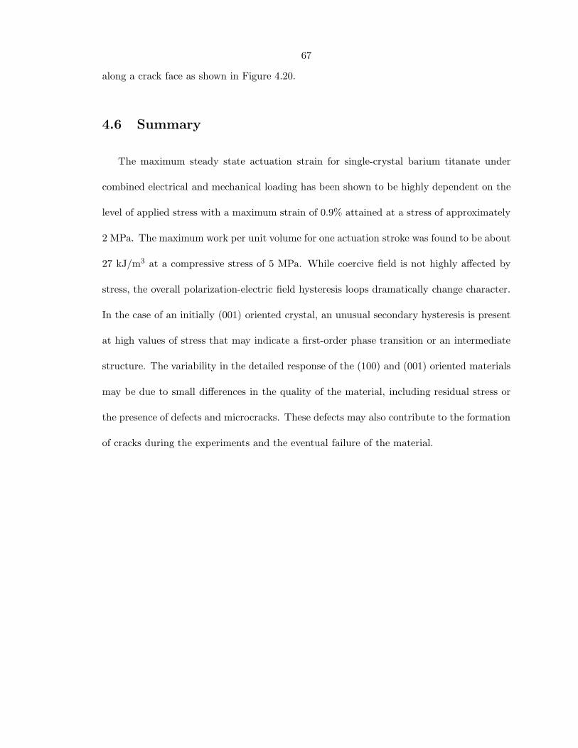
67
along a crack face as shown in Figure 4.20.
4.6 Summary
The maximum steady state actuation strain for single-crystal barium titanate under
combined electrical and mechanical loading has been shown to be highly dependent on the
level of applied stress with a maximum strain of 0.9% attained at a stress of approximately
2 MPa. The maximum work per unit volume for one actuation stroke was found to be about
27 kJ/m3 at a compressive stress of 5 MPa. While coercive field is not highly affected by
stress, the overall polarization-electric field hysteresis loops dramatically change character.
In the case of an initially (001) oriented crystal, an unusual secondary hysteresis is present
at high values of stress that may indicate a first-order phase transition or an intermediate
structure. The variability in the detailed response of the (100) and (001) oriented materials
may be due to small differences in the quality of the material, including residual stress or
the presence of defects and microcracks. These defects may also contribute to the formation
of cracks during the experiments and the eventual failure of the material.

68
(a)
0 20 40 60−15
−10
−5
0
5
10
15
Ele
ctric
Fie
ld (
kV/c
m)
0 20 40 60−0.2
0
0.2
0.4
0.6
0.8
1
stra
in (
%)
Time (sec.)
Elect. fieldStrain
(b)
−10 −5 0 5 10−0.2
0
0.2
0.4
0.6
0.8
1
Electric Field (kV/cm)
stra
in (
%)
Figure 4.1: (a) Electric field and strain vs. time and (b) strain vs. electric field for (100)oriented crystal at 1.07 MPa compressive stress.

69
(a)
0 20 40 60−15
−10
−5
0
5
10
15
Ele
ctric
Fie
ld (
kV/c
m)
0 20 40 60−0.4
−0.2
0
0.2
0.4
Pol
ariz
atio
n (C
/m2 )
Time (sec.)
Elect. fieldPolarization
(b)
−10 −5 0 5 10−0.4
−0.2
0
0.2
0.4
Electric Field (kV/cm)
Pol
ariz
atio
n (C
/m2 )
Figure 4.2: (a) Electric field and polarization vs. time and (b) polarization vs. electric fieldfor (100) oriented crystal at 1.07 MPa compressive stress.

70
−10 −5 0 5 10
0
0.2
0.4
0.6
0.8
1
Electric Field (kV/cm)
stra
in (
%)
σ = 0 MPa
−10 −5 0 5 10
0
0.2
0.4
0.6
0.8
1
Electric Field (kV/cm)
stra
in (
%)
σ = −0.36 MPa
−10 −5 0 5 10
0
0.2
0.4
0.6
0.8
1
Electric Field (kV/cm)
stra
in (
%)
σ = −0.72 MPa
−10 −5 0 5 10
0
0.2
0.4
0.6
0.8
1
Electric Field (kV/cm)
stra
in (
%)
σ = −1.07 MPa
−10 −5 0 5 10
0
0.2
0.4
0.6
0.8
1
Electric Field (kV/cm)
stra
in (
%)
σ = −1.78 MPa
Figure 4.3: Strain vs. electric field for five values of compressive stress with an initially(100) oriented crystal with input amplitude of ±10 kV/cm.
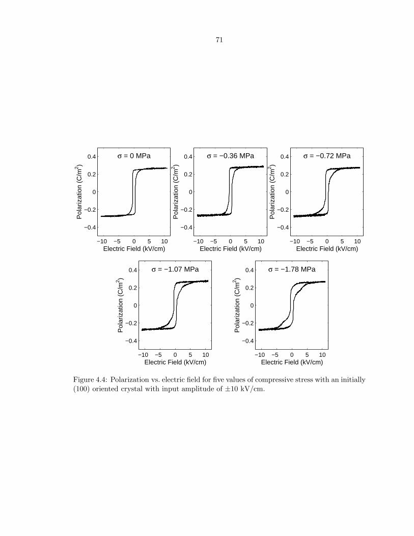
71
−10 −5 0 5 10
−0.4
−0.2
0
0.2
0.4
Electric Field (kV/cm)
Pol
ariz
atio
n (C
/m2 )
σ = 0 MPa
−10 −5 0 5 10
−0.4
−0.2
0
0.2
0.4
Electric Field (kV/cm)
Pol
ariz
atio
n (C
/m2 )
σ = −0.36 MPa
−10 −5 0 5 10
−0.4
−0.2
0
0.2
0.4
Electric Field (kV/cm)
Pol
ariz
atio
n (C
/m2 )
σ = −0.72 MPa
−10 −5 0 5 10
−0.4
−0.2
0
0.2
0.4
Electric Field (kV/cm)
Pol
ariz
atio
n (C
/m2 )
σ = −1.07 MPa
−10 −5 0 5 10
−0.4
−0.2
0
0.2
0.4
Electric Field (kV/cm)
Pol
ariz
atio
n (C
/m2 )
σ = −1.78 MPa
Figure 4.4: Polarization vs. electric field for five values of compressive stress with an initially(100) oriented crystal with input amplitude of ±10 kV/cm.

72
−0.4 −0.2 0 0.2 0.4
0
0.2
0.4
0.6
0.8
1
stra
in (
%)
Polarization (C/m2)
σ = 0 MPa
−0.4 −0.2 0 0.2 0.4
0
0.2
0.4
0.6
0.8
1
stra
in (
%)
Polarization (C/m2)
σ = −0.36 MPa
−0.4 −0.2 0 0.2 0.4
0
0.2
0.4
0.6
0.8
1
stra
in (
%)
Polarization (C/m2)
σ = −0.72 MPa
−0.4 −0.2 0 0.2 0.4
0
0.2
0.4
0.6
0.8
1
stra
in (
%)
Polarization (C/m2)
σ = −1.07 MPa
−0.4 −0.2 0 0.2 0.4
0
0.2
0.4
0.6
0.8
1
stra
in (
%)
Polarization (C/m2)
σ = −1.78 MPa
Figure 4.5: Strain vs. polarization for five values of compressive stress with an initially (100)oriented crystal with input amplitude of ±10 kV/cm.

73
−10 −5 0 5 10
0
0.2
0.4
0.6
0.8
1
Electric Field (kV/cm)
stra
in (
%)
σ = 0 MPa
−10 −5 0 5 10
0
0.2
0.4
0.6
0.8
1
Electric Field (kV/cm)
stra
in (
%)
σ = −0.36 MPa
−10 −5 0 5 10
0
0.2
0.4
0.6
0.8
1
Electric Field (kV/cm)
stra
in (
%)
σ = −1.07 MPa
−10 −5 0 5 10
0
0.2
0.4
0.6
0.8
1
Electric Field (kV/cm)
stra
in (
%)
σ = −2.14 MPa
−10 −5 0 5 10
0
0.2
0.4
0.6
0.8
1
Electric Field (kV/cm)
stra
in (
%)
σ = −2.85 MPa
−10 −5 0 5 10
0
0.2
0.4
0.6
0.8
1
Electric Field (kV/cm)
stra
in (
%)
σ = −3.92 MPa
Figure 4.6: Strain vs. electric field for six values of compressive stress with an initially (001)oriented crystal with input amplitude of ±7.5 kV/cm.

74
−10 −5 0 5 10
−0.4
−0.2
0
0.2
0.4
Electric Field (kV/cm)
Pol
ariz
atio
n (C
/m2 )
σ = 0 MPa
−10 −5 0 5 10
−0.4
−0.2
0
0.2
0.4
Electric Field (kV/cm)
Pol
ariz
atio
n (C
/m2 )
σ = −0.36 MPa
−10 −5 0 5 10
−0.4
−0.2
0
0.2
0.4
Electric Field (kV/cm)
Pol
ariz
atio
n (C
/m2 )
σ = −1.07 MPa
−10 −5 0 5 10
−0.4
−0.2
0
0.2
0.4
Electric Field (kV/cm)
Pol
ariz
atio
n (C
/m2 )
σ = −2.14 MPa
−10 −5 0 5 10
−0.4
−0.2
0
0.2
0.4
Electric Field (kV/cm)
Pol
ariz
atio
n (C
/m2 )
σ = −2.85 MPa
−10 −5 0 5 10
−0.4
−0.2
0
0.2
0.4
Electric Field (kV/cm)
Pol
ariz
atio
n (C
/m2 )
σ = −3.92 MPa
Figure 4.7: Polarization vs. electric field for six values of compressive stress with an initially(001) oriented crystal with input amplitude of ±7.5 kV/cm.

75
−0.4 −0.2 0 0.2 0.4
0
0.2
0.4
0.6
0.8
1
stra
in (
%)
Polarization (C/m2)
σ = 0 MPa
−0.4 −0.2 0 0.2 0.4
0
0.2
0.4
0.6
0.8
1
stra
in (
%)
Polarization (C/m2)
σ = −0.36 MPa
−0.4 −0.2 0 0.2 0.4
0
0.2
0.4
0.6
0.8
1
stra
in (
%)
Polarization (C/m2)
σ = −1.07 MPa
−0.4 −0.2 0 0.2 0.4
0
0.2
0.4
0.6
0.8
1
stra
in (
%)
Polarization (C/m2)
σ = −2.14 MPa
−0.4 −0.2 0 0.2 0.4
0
0.2
0.4
0.6
0.8
1
stra
in (
%)
Polarization (C/m2)
σ = −2.85 MPa
−0.4 −0.2 0 0.2 0.4
0
0.2
0.4
0.6
0.8
1st
rain
(%
)
Polarization (C/m2)
σ = −3.92 MPa
Figure 4.8: Strain vs. polarization for six values of compressive stress with an initially (001)oriented crystal with input amplitude of ±7.5 kV/cm.

76
−8 −6 −4 −2 0 2 4 6 8−0.3
−0.2
−0.1
0
0.1
0.2
0.3 ps1
Electric field (kV/cm)
Pol
ariz
atio
n (C
/m2 ) p
s2
σ = −3.2 MPa
Figure 4.9: Primary (Ps1) and secondary (Ps2) spontaneous polarization for (001) orientedcrystal at 3.2 MPa compressive stress.

77
0
0.1
0.2
0.3
0.4
0.5
0.6
0.7
0.8
0.9
1
0 0.5 1 1.5 2 2.5 3 3.5 4 4.5 5Compressive Stress (MPa)
Act
uat
ion
Str
ain
(%)
(001) Crystal(001) Crystal(100) Crystal
Figure 4.10: Actuation strain vs. compressive stress for barium titanate.
0
100
200
300
400
500
600
0 0.5 1 1.5 2 2.5 3 3.5 4 4.5 5
Compressive Stress (MPa)
Co
erci
ve F
ield
(V/c
m)
(001) Crystal(001) Crystal(100) Crystal
Figure 4.11: Coercive field vs. compressive stress for barium titanate.

78
-6 -4 -2 0 2 4 6-0.1
-0.05
0
0.05
0.1
Electric field (kV/cm)
dε/d
E (
%/k
V/c
m)
1 2
12 1 - Saturation
2 - Desaturation
Figure 4.12: Derivative of strain with respect to electric field for (100) oriented crystal at1.07 MPa compressive stress.
0
1
2
3
4
5
-8 -6 -4 -2 0 2 4 6 8Electric Field (kV/cm)
(100)
(001) (001)
Com
pres
sive
Str
ess
(MP
a)
ExperimentPath
Predicted/ Saturation
Desaturation/
// (100) Crystal
(001) Crystal
Figure 4.13: Comparison of predicted equilibrium phase diagram and experimental satura-tion and desaturation of strain with respect to electric field.

79
1.E+02
1.E+03
1.E+04
1.E+05
0 2 4 6 8 10Compressive Stress (MPa)
Wor
k/V
olum
e (J
/m3)
(100) Crystal(001) Crystal(001) CrystalUpper Bound
0
20
40
60
80
100
% o
f Upp
er B
ound
Figure 4.14: Work per unit volume (per actuation stroke) vs. compressive stress for ±7500and ±10,000 V/cm electric field range. Upper bound is calculated using 1.1% actuationstrain.

80
(a)
-10 -5 0 5 10Electric Field (kV/cm)
0
0.2
0.4
0.6
0.8
1
stra
in(%
)
0.05 Hz.0.1 Hz.0.5 Hz.1.0 Hz.
= -1.07 MPaσ
(b)
-10 -5 0 5 10Electric Field (kV/cm)
0
0.2
0.4
0.6
0.8
1
stra
in(%
)
0.05 Hz.0.1 Hz.0.5 Hz.1.0 Hz.
= -2.14 MPaσ
Figure 4.15: Strain response at frequencies from 0.05 to 1.0 Hz with (a) 1.07 MPa and (b)2.14 MPa compressive stress.

81
−6 −4 −2 0 2 4 6
0
0.2
0.4
0.6
0.8
1
Electric field (kV/cm)
stra
in (
%)
1
2
3 4
5
−6 −4 −2 0 2 4 6−0.4
−0.2
0
0.2
0.4
Electric field (kV/cm)
Pol
ariz
atio
n (C
/m2 )
12
3
4 5
Figure 4.16: Sample images of domain patterns from experiment at 1.07 MPa compressivestress with corresponding strain and polarization.

82
−5 0 50
0.1
0.2
0.3
0.4
0.5
0.6in
tens
ity
Electric field (kV/cm)−5 0 5
0
0.2
0.4
stra
in (
%)
σ = −0.72 MPa
−5 0 50
0.1
0.2
0.3
0.4
0.5
0.6
inte
nsity
Electric field (kV/cm)−5 0 5
0
0.2
0.4
0.6
0.8
1
stra
in (
%)
σ = −1.07 MPa
−5 0 50
0.1
0.2
0.3
0.4
0.5
0.6
inte
nsity
Electric field (kV/cm)−5 0 5
0
0.2
0.4
0.6
0.8
1
stra
in (
%)
σ = −2.14 MPa
−5 0 50
0.1
0.2
0.3
0.4
0.5
0.6
inte
nsity
Electric field (kV/cm)−5 0 5
0
0.2
0.4
0.6
0.8
1
stra
in (
%)
σ = −2.85 MPa
−5 0 50
0.1
0.2
0.3
0.4
0.5
0.6
inte
nsity
Electric field (kV/cm)−5 0 5
0
0.2
0.4
0.6
0.8
1
stra
in (
%)
σ = −3.92 MPa
intensitystrain
Figure 4.17: Comparison of integrated image intensity and strain vs. electric field at fivestress levels.
83
−5 0 50
0.1
0.2
0.3
0.4
0.5
0.6
inte
nsity
Electric field (kV/cm)−5 0 5
0.15
0.2
0.25
0.3
|P| (
C/m
2 )
σ = −0.72 MPa
−5 0 50
0.1
0.2
0.3
0.4
0.5
0.6
Electric field (kV/cm)−5 0 5
0.15
0.2
0.25
0.3
|P| (
C/m
2 )
σ = −1.07 MPa
−5 0 50
0.1
0.2
0.3
0.4
0.5
0.6
inte
nsity
Electric field (kV/cm)−5 0 5
0.15
0.2
0.25
0.3
|P| (
C/m
2 )
σ = −2.14 MPa
−5 0 50
0.1
0.2
0.3
0.4
0.5
0.6
Electric field (kV/cm)−5 0 5
0.15
0.2
0.25
0.3
|P| (
C/m
2 )
σ = −2.85 MPa
−5 0 50
0.1
0.2
0.3
0.4
0.5
0.6
inte
nsity
Electric field (kV/cm)−5 0 5
0.15
0.2
0.25
0.3
|P| (
C/m
2 )
σ = −3.92 MPaintensitypolarization
(absolute value)
Figure 4.18: Comparison of integrated image intensity and polarization (absolute value)vs. electric field at five stress levels.

84
Initial (100) orientation Initial (001) orientation
Figure 4.19: Pictures of damaged crystals after experiments.
Figure 4.20: Spark path through initially polydomain crystal along a crack face.

85
References
[1] F. Jona and G. Shirane, Ferroelectric Crystals, Pergamon, New York, 1962. Reprint,
Dover, New York, 1993.
[2] Z. Li, C. M. Foster, X.-H. Dai, X.-Z. Xu, S.-K. Chan, and D. J. Lam, “Piezoelectrically-
induced switching of 90 domains in tetragonal BaTiO3 and PbTiO3 investigated by
micro-Raman spectroscopy,” J. Appl. Phys. 71, pp. 4481–4486, 1992.
[3] T. Mitsui, K. H. Hellwege, and A. M. Hellwege, eds., Ferroelectrics and related sub-
stances, vol. 16A of Landolt-Boernstein Numerical data and functional relationships in
science and technology, Group III, pp. 66–77, 333–334, 350. Spring-Verlag, New York,
1981.
[4] C. S. Lynch, “The effect of uniaxial stress on the electro-mechanical response of 8/65/35
PLZT,” Acta mater. 44, pp. 4137–4148, 1996.
[5] E. J. Huibregtse and D. R. Young, “Triple hysteresis loops and the free-energy function
in the vicinity of the 5 transition in BaTiO3,” Phys. Rev. 103(6), pp. 1705–1711, 1956.

86
Chapter 5 CONCLUSIONS
An experimental setup has been designed to investigate large strain actuation in single
crystal ferroelectrics under combined electrical and mechanical loading. An investigation of
the stress dependence of the electrostrictive response has been carried out with in situ obser-
vation of the domain pattern under constant compressive stress and variable electric field.
Experiments have been performed on initially single domain crystals of barium titanate
(BaTiO3) with (100) and (001) orientation at compressive stresses between 0 and 5 MPa.
Global strain and polarization histories were recorded. The electrostrictive response has
been shown to be highly dependent on the level of applied stress with a maximum strain
of 0.9% measured at a compressive stress of about 2 MPa. Coercive field was found to
be insensitive to stress. The response was found to be repeatable for multiple crystals of
different orientation and from different suppliers. An unusual secondary hysteresis has been
observed in the polarization signal at high levels of stress that indicates an intermediate
structural configuration, possibly the orthorhombic state. Polarized light microscopy has
been used to observe the evolution of the domain pattern simultaneously with the strain and
polarization measurement. An average image intensity has been calculated which correlates
well with the measured strain and polarization signals and gives insight into the level of
inhomogeneity of the crystal deformation.
An initial hypothesis was presented from the theory of Shu and Bhattacharya that large
strain actuation in single-crystal ferroelectrics is possible through 90 domain motion and
switching under combined compressive prestress and electric field loading [1]. The global

87
measurements (strain and polarization) and local observations (polarized light microscopy)
presented in this dissertation clearly support this hypothesis. The theory and experimental
evidence have been used as the basis for a patent application for a large strain actuator [2].
The work per unit volume has been used as a figure of merit for comparing the performance
of the actuator with other devices. The maximum experimental work per unit volume for
the experimental conditions is about 3×10⁴ J/m3, well below the desired range of 106 J/m3.
For the current bulk crystal material, this range seems out of reach given the high voltages
required. Performance on the order of 105 J/m3, however, would be easily attainable with
stresses of 10 MPa and reasonable electric fields of ±25–30 kV/cm. Higher performance
may be possible with thin films which require lower voltages. Other bulk materials can be
explored that may also offer better performance.
5.1 Suggestions for Future Work
Suggestions for further experiments are presented with descriptions of an improved ap-
paratus and alternate materials. Future investigations will add to the understanding of the
mechanics of ferroelectrics and the possible applications of the large strain electrostrictive
response of ferroelectrics that has been demonstrated in this work.
Additional Experiments with Barium Titanate
In situ microscopy has been used to make observations of domain patterns but many
unanswered questions need to be addressed. Images have been captured for only one cycle
in each experiment when the crystal is assumed to have reached a steady state. It would
be interesting to see whether the detailed domain pattern evolves identically in each cycle
by capturing images during several cycles of the same experiment. The inhomogeneity of

88
deformation of the crystals was pointed out in chapter 4. To get some further information
of the level of inhomogeneity outside the field of view of the video images, composite images
of the entire crystal could be taken at constant electric field. This would require manual or
automated movement of the microscope XY translation stage to capture about 100 images
covering the entire area.
Further experiments are required to explore the secondary hysteresis behavior that has
been observed at high stress levels. In situ X-ray diffraction could be used to get structural
information about the intermediate phase. In addition, experiments can be performed at
low temperatures close to the tetragonal-orthorhombic phase transition. If the intermediate
structure is the orthorhombic phase, the secondary hysteresis should become visible at lower
levels of stress. High temperature experiments should eliminate the secondary hysteresis and
increase the mobility of domains near the Curie temperature, reducing hysteresis. Finally,
the frequency response needs to be well characterized and the upper limit of the rate of the
large strain response must be determined.
Alternate Materials
Similar experiments to those described can be performed on alternate materials includ-
ing bulk crystals, thin films, and texture ceramics. The most obvious extension is to repeat
the experiments of the type described in this dissertation on bulk lead titanate which has
a spontaneous strain of approximately 6%. Another potential material may be potassium
niobate, which is orthorhombic at room temperature. Different orientations of barium ti-
tanate may be used to purposely induce the orthorhombic phase transition. In addition to
pure materials, solid solutions (e.g., (PbxBa1−x)TiO3) may be used to get optimal combi-
nations of strain and saturation field. Complex solid solutions with other perovskites may

89
be attempted. A list of ferroelectric and antiferroelectric perovskites is shown in Table
5.1. Large strain actuation in certain textured ceramics has been predicted by Shu and
Bhattacharya [1] and should be tested if such materials can be produced.
Thin films are the most suitable materials for microactuator applications and MEMS.
Single crystal films of barium titanate, lead titanate, and solid solutions, such as PZT and
(PbxBa1−x)TiO3, as well as textured polycrystalline films are suitable candidates. Films
are also useful for studying the mechanism of domain switching since it may be possible
to have a single domain through the thickness of the film. Domain mobility measurements
could be made by measuring the velocity of the domain wall under different driving forces.
Such measurements would be possible using optical microscopy. The depth of field would
be sufficient to focus on the domain wall through the entire thickness of the film. Suitable
electric fields could be applied without requiring high voltages and, while it may be difficult
to apply uniaxial compressive stress, in-plane tension may be easily applied in partially
released films.
Experimental Apparatus
Improvements to the current experimental setup could offer more flexibility in the choice
of loading conditions and test materials. For instance, an improved loading mechanism con-
sisting of a compact, screw driven test frame with a compliant spring for loading could be
used for load control experiments with variable stress to measure the stress-strain behavior
at constant electric field. The same setup could be used for constant load experiments at a
wider range of stresses. Such a system could be designed for a wider frequency range than
the current system, allowing more experiments to examine the frequency response of the
material. Temperature control could be incorporated to perform both low and high tem-

90
perature experiments mentioned earlier. Other possible improvements to the experimental
setup include construction of a high impedance charge amplifier that would eliminate the
charge signal decay described in Chapter 3. An improved higher resolution microscope
could be constructed. Magnification could be increased by including an eyepiece in front
of the camera. Magnification could be increased by up to 10 times. Stronger objectives
could be used to further increase the magnification. For higher magnification use, however,
a stiffer microscope stand may be needed to reduce vibration. A digital video camera could
be used to increase image resolution and reduce image noise. A digital camera would also
allow more precise timing and, possibly, higher frame rates.

91
Table 5.1: Ferroelectric and antiferroelectric perovskites.
Curie Temp. Room Temp. Lattice ParametersSubstance
(C) Phase (at 25C)a = 3.9920 A, c = 4.0361 A
BaTiO3 120C Tetragonal(c/a = 1.011)a = 3.904 A, c = 4.152 A
PbTiO3 490C Tetragonal(c/a = 1.064)a = 3.997 A, b = 5.695 A,c = 5.721 A
pseudotetragonal lattice parameters:a′ = c′ = 4.0375 A, b′ = 3.9711 A
KNbO3 418C Orthorhombic
β = 90 15′, (c′/b′ = 1.0167)a = 5.4941 A, b = 7.7508 A,
NaTaO3† 480C Orthorhombic
c = 5.5130 AAntiferroelectric Substances
a = c = 2 · (3.9150(2)) A,b = 4 · (3.8798(2)) ANaNbO3 365C Orthorhombicα = γ = 90, β = 90 40(3)′
monoclinic cell parameters:amon = cmon = 4.1604 A,bmon = 4.1111 A
PbZrO3 230C Orthorhombic
β = 90 05′ 28′′
a = 5.8572 A, b = 11.689 A,PbHfO3
† 163C Orthorhombicc = 4.0971 Aa = 5.5014 A, b = 5.6607 A,
CdHfO3† 600C Orthorhombic
c = 7.969 A† Possible ferro/antiferroelectric behaviorSource: [3]

92
References
[1] Y. C. Shu and K. Bhattacharya, “Domain patterns and macroscopic behavior of ferro-
electric materials,” Phil. Mag. A (submitted) .
[2] E. Burcsu, K. Bhattacharya, G. Ravichandran, and Y. C. Shu, “Electrostrictive actuator
using ferroelectric single crystal,” US Patent pending, submitted Mar. 31, 2000.
[3] T. Mitsui, K. H. Hellwege, and A. M. Hellwege, eds., Ferroelectrics and related sub-
stances, vol. 16A of Landolt-Boernstein Numerical data and functional relationships in
science and technology, Group III, pp. 66–77, 333–334, 350. Spring-Verlag, New York,
1981.

93
Bibliography
Note: Citation numbers in text refer to References section at the end of each chapter.
[1] A. J. Bell, “Multilayer ceramic processing,” in Ferroelectric Ceramics: Tutorial reviews,
theory, processing, and applications, N. Setter and E. L. Colla, eds., pp. 241–271, Monte
Verita, Zurich, 1993.
[2] E. Burcsu, K. Bhattacharya, G. Ravichandran, and Y. C. Shu, “Electrostrictive actu-
ator using ferroelectric single crystal,” US Patent pending, submitted Mar. 31, 2000.
[3] W. Chen and C. S. Lynch, “A micro-electro-mechanical model for polarization switch-
ing of ferroelectric materials,” Acta mater. 46, pp. 5303–5311, 1998.
[4] L. E. Cross, “Ferroelectric ceramics: Tailoring properties for specific applications,” in
Ferroelectric Ceramics: Tutorial reviews, theory, processing, and applications, N. Setter
and E. L. Colla, eds., pp. 1–85, Monte Verita, Zurich, 1993.
[5] L. E. Cross, “Ferroelectric materials for electromechanical transducer applications,”
Jpn. J. Appl. Phys. Pt. 1 34, pp. 2525–2532, 1995.
[6] D. Damjanovic, “Ferroelectric, dielectric and piezoelectric properties of ferroelectric
thin films and ceramics,” Rep. Prog. Phys. 61, pp. 1267–1324, 1998.
[7] A. F. Devonshire, “Theory of barium titanate – Part I,” Phil. Mag. 40, pp. 1040–1063,
1949.

94
[8] A. F. Devonshire, “Theory of barium titanate – Part II,” Phil. Mag. 42(333), pp. 1065–
1079, 1951.
[9] A. F. Devonshire, “Theory of ferroelectrics,” Phil. Mag. Suppl. (Advances in Physics)
3(10), pp. 85–130, 1954.
[10] E. Fatuzzo and W. J. Merz, Ferroelectricity, Wiley, Interscience, New York, 1967.
[11] H. Fu and R. E. Cohen, “Polarization rotation mechanism for ultrahigh electromechan-
ical response in single-crystal piezoelectrics,” Nature 403, pp. 281–283, 2000.
[12] G. H. Haertling, “Rainbow ceramics – a new type of ultra-high-displacement actuator,”
Amer. Ceram. Soc. Bull. 73(1), pp. 93–96, 1994.
[13] L. L. Hench and J. K. West, Principles of Electronic Ceramics, Wiley, New York, 1990.
[14] E. J. Huibregtse and D. R. Young, “Triple hysteresis loops and the free-energy function
in the vicinity of the 5 transition in BaTiO3,” Phys. Rev. 103(6), pp. 1705–1711, 1956.
[15] S. Inoue, Video Microscopy, Plenum Press, New York, 1986.
[16] B. Jaffe, W. R. Cook, and H. Jaffe, Piezoelectric Ceramics, Academic Press, New York,
1971.
[17] F. Jona and G. Shirane, Ferroelectric Crystals, Pergamon, New York, 1962. Reprint,
Dover, New York, 1993.
[18] P. Krulevitch, A. P. Lee, P. B. Ramsey, J. C. Trevino, J. Hamilton, and M. A. Northrup,
“Thin film shape memory alloy microactuators,” J. MEMS 5(4), pp. 270–282, 1996.
[19] S. P. Li, A. S. Bhalla, R. E. Newnham, L. E. Cross, and C. Y. Huang, “90 domain
reversal in Pb(ZrxTi1−x)O3 ceramics,” J. Mater. Sci. 29, pp. 1290–1294, 1994.
95
[20] Z. Li, S.-K. Chan, M. H. Grimsditch, and E. S. Zouboulis, “The elastic and elec-
tromechanical properties of tetragonal BaTiO3 single crystals,” J. Appl. Phys. 70(12),
pp. 7327–7332, 1991.
[21] Z. Li, C. M. Foster, X.-H. Dai, X.-Z. Xu, S.-K. Chan, and D. J. Lam, “Piezoelectrically-
induced switching of 90 domains in tetragonal BaTiO3 and PbTiO3 investigated by
micro-Raman spectroscopy,” J. Appl. Phys. 71, pp. 4481–4486, 1992.
[22] E. A. Little, “Dynamic behavior of domain walls in barium titanate,” Phys. Rev. 98,
pp. 978–984, 1955.
[23] C. S. Lynch, “The effect of uniaxial stress on the electro-mechanical response of 8/65/35
PLZT,” Acta mater. 44, pp. 4137–4148, 1996.
[24] R. C. Miller and A. Savage, “Motion of 180 domain walls in metal electroded barium
titanate crystals as a function of electric field and sample thickness,” J. Appl. Phys.
31, pp. 662–669, 1960.
[25] T. Mitsui, K. H. Hellwege, and A. M. Hellwege, eds., Ferroelectrics and related sub-
stances, vol. 16A of Landolt-Boernstein Numerical data and functional relationships in
science and technology, Group III, pp. 66–77, 333–334, 350. Spring-Verlag, New York,
1981.
[26] W. Y. Pan, C. Q. Dam, Q. M. Zhang, and L. E. Cross, “Large displace-
ment transducers based on electric-field forced phase-transitions in the tetragonal
(Pb0.97La0.02)(Ti,Zr,Sn)O3 family of ceramics,” J. Appl. Phys. 66(12), pp. 6014–6023,
1989.

96
[27] S. E. Park and T. R. Shrout, “Ultrahigh strain and piezoelectric behavior in relaxor
based ferroelectric single crystals,” J. Appl. Phys. 82, pp. 1804–1808, 1997.
[28] S. E. Park, S. Wada, L. E. Cross, and T. R. Shrout, “Crystallographically engi-
neered BaTiO3 single crystals for high-performance piezoelectrics,” J. Appl. Phys. 86,
pp. 2746–2750, 1999.
[29] C. B. Sawyer and C. H. Tower, “Rochelle salt as a dielectric,” Phys. Rev. 35, pp. 269–
273, 1930. [see Jaffe, Piezoelectric Ceramics, Acad. Press, 1971].
[30] H. Schmid, “Polarized light microscopy (PLM) of ferroelectric and ferroelastic domains
in transmitted and reflected light,” in Ferroelectric Ceramics: Tutorial reviews, theory,
processing, and applications, N. Setter and E. L. Colla, eds., pp. 107–126, Monte Verita,
Zurich, 1993.
[31] J. F. Scott, “The physics of ferroelectric ceramic thin films for memory applications,”
Ferroelectrics Review 1, pp. 1–129, 1998.
[32] Y. C. Shu and K. Bhattacharya, “Domain patterns and macroscopic behavior of ferro-
electric materials,” Phil. Mag. A (submitted) .
[33] B. A. Strukov and A. P. Levanyuk, Ferroelectric Phenomena in Crystals, Springer-
Verlag, New York, 1998.
[34] K. Uchino, Ferroelectric Devices, Marcel Decker, New York, 2000.
[35] S. Wada, S. Suzuki, T. Noma, T. Suzuki, M. Osada, M. Kakihana, S. E. Park, L. E.
Cross, and T. R. Shrout, “Enhanced piezoelectric property of barium titanate single
crystals with engineered domain configurations,” Jpn. J. Appl. Phys. 38, pp. 5505–
5511, 1999.

97
[36] Y. Xu, Ferroelectric Materials, North-Holland, New York, 1991.


![Index [ftp.feq.ufu.br]ftp.feq.ufu.br/Luis_Claudio/Segurança/Safety/Double/fire_handbook... · Backdraft Explosion 174 Barium 216 Barium Carbonate 300 Barium Chlorate 300 Barium Nitrate](https://img.dokumen.tips/doc/110x75/5ea2585052451660ed3ed304/index-ftpfequfubrftpfequfubrluisclaudioseguranasafetydoublefirehandbook.jpg)