Embed Size (px)
Citation preview

Introduction to Solids
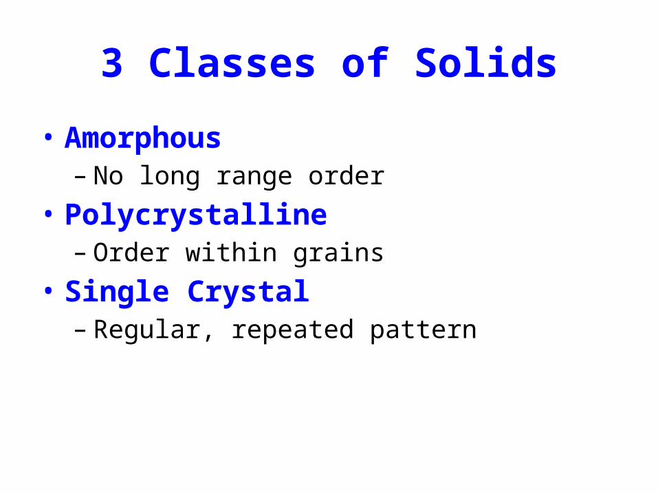
3 Classes of Solids
• Amorphous– No long range order
• Polycrystalline– Order within grains
• Single Crystal– Regular, repeated pattern

Crystal Solid
• Single crystal – repetition of a unit cell
• Crystal lattice– Array of corners of unit cells
• Symmetry– Used to classify the crystal– Ex. Cubic symmetry

3 Subclasses of Cubic Crystals
• Simple– The sites for atoms are at the corners of the cubes
• Body-Centered-Cubic (bcc)– The sites for the atoms are at the corners of the
cubes• Face-Centered-Cubic (fcc)– The sites for the atoms are at the corners and at the
centers of each face of the cube
Note: Show figures

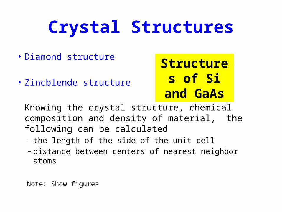
Crystal Structures
• Diamond structure
• Zincblende structure
Knowing the crystal structure, chemical composition and density of material, the following can be calculated– the length of the side of the unit cell– distance between centers of nearest neighbor atoms
Note: Show figures
Structures of Si and GaAs


Crystal Structures
• X-ray diffraction – Method used to determine the plane and
direction of a crystal
• The specification of particular planes and directions is made through the use of Miller indices

• Finding Milles indices of a plane in a crystal– Choose coordinate access along the principal
directions in the crystal (long the unit cell edges)
– Take the 3 numbers that result as the intersection of a plane with the 3 axes• Take their reciprocals• Multiply the results by the smallest value that will give
3 integers• These 3 integers are the Mille indices of the plane

• Finding Milles indices of a direction in a crystal– Take the 3 components of a vector in that
direction along the 3 axes
– Multiply these components by whatever is needed to reduce them to the smallest set of integers
– These integers are the Miller indices of the direction
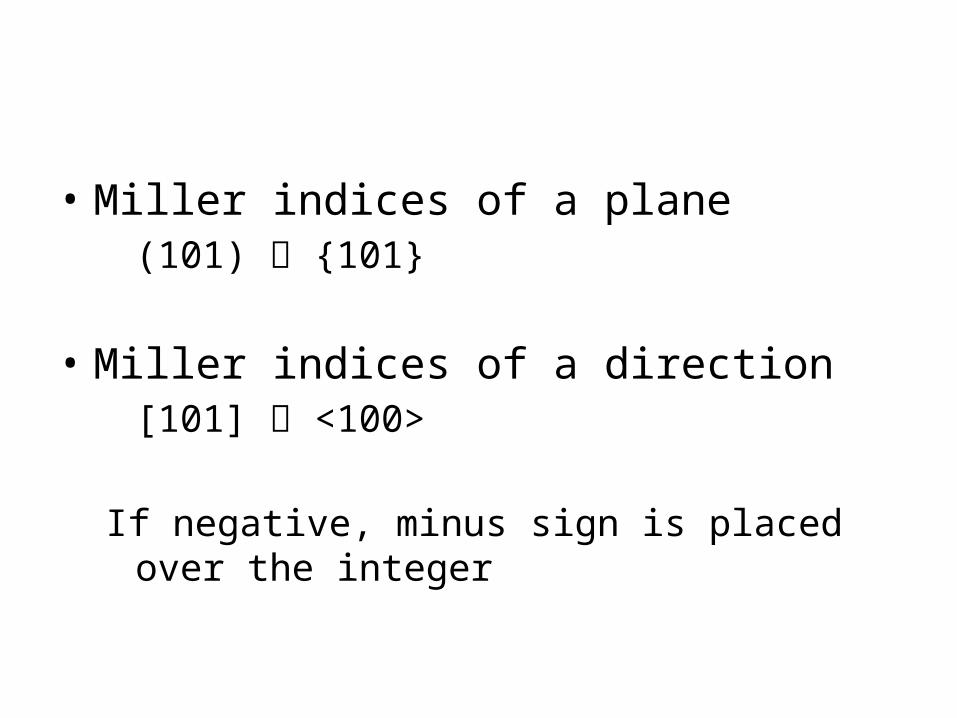
• Miller indices of a plane(101) {101}
• Miller indices of a direction[101] <100>
If negative, minus sign is placed over the integer
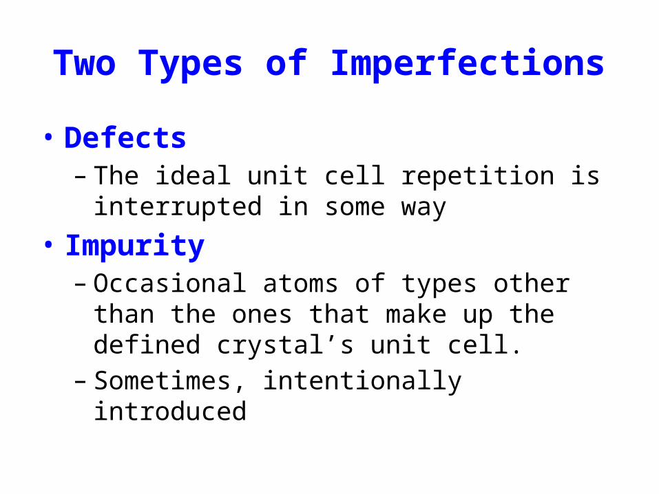
Two Types of Imperfections
• Defects– The ideal unit cell repetition is interrupted in some
way • Impurity – Occasional atoms of types other than the ones
that make up the defined crystal’s unit cell.– Sometimes, intentionally introduced

Impurity
• Doping – adding impurities
• Dopant – the added material

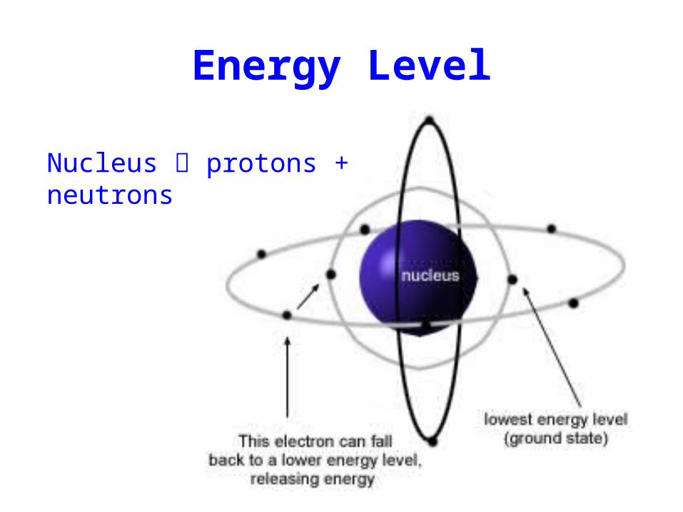
Energy Level
• Single atoms– Only one electron can occupy a given state
(Pauli exclusion principle)– Different states different energies associated– Ground state electrons of an atom are in the
lowest possible energy states– Excited state when an electron moves to the
state of higher energy
Energy Level
Nucleus protons + neutrons


Energy Level
• Principal energy level 123456
• Sublevel1s2s 2p3s 3p 3d4s 4p 4d 4f5s 5p 5d 5f 5g6s 6p 6d 6f 6g 6h

Energy Level
• the 1s energy level is always the lowest energy level of all principal energy levels
• for each principal energy level, the s sublevel is also the lowest energy sublevel
• The diagram at the right illustrates the determination of order of sublevels by increasing energy Source: http://library.thinkquest.org/15567/lessons/2.html

Orbital
• A region within a sublevel where electrons may be found• In each orbital, there can be a maximum of two electrons
– Each s sublevel has a single orbital– Each p sublevel has 3 orbitals – Each d sublevel has 5 orbitals– Each f sublevel has 7 orbitals
• Thus, any s sublevel can have two electrons, while any p sublevel can have 6 electrons, and so on
No. of sublevels No. of orbitals (s, p, d, f) Total No. of orbitals Maximum no. of
electrons
1234
(1)(1, 3)
(1, 3, 5)(1, 3, 5, 7)
149
16
28
1832

Band Gap
Source: http://hyperphysics.phy-astr.gsu.edu/hbase/solids/band.html

Fermi-Level• Extra levels have been added by the impurities • In n-type material there are electron energy levels near the
top of the band gap so that they can be easily excited into the conduction band
• In p-type material, extra holes in the band gap allow excitation of valence band electrons, leaving mobile holes in the valence band

Video Links CLASSES OF SOLIDShttp://www.youtube.com/watch?v=SJsckwYxfgY&feature=related
CRYSTAL LATTICE Lattice Structures Part 1 (Cubic, body-centered, Face centered --> unit cell)http://www.youtube.com/watch?v=Rm-i1c7zr6Q&feature=related
SAND TO SILICON TO IChttp://www.youtube.com/watch?v=Q5paWn7bFg4
SILICON RUN 1http://www.youtube.com/watch?v=ATt5dwdKt9I