Embed Size (px)
Citation preview

1
Chapter 7 <1>
Digital Design and Computer Architecture, 2nd Edition
Chapter 7
David Money Harris and Sarah L. Harris
Chapter 7 <2>
Chapter 7 :: Topics
• Introduction• Performance Analysis• Single‐Cycle Processor• Multicycle Processor• Pipelined Processor• Exceptions• Advanced Microarchitecture
Chapter 7 <3>
• Microarchitecture: how to implement an architecture in hardware
• Processor:– Datapath: functional blocks– Control: control signals
Physics
Devices
AnalogCircuits
DigitalCircuits
Logic
Micro-architecture
Architecture
OperatingSystems
ApplicationSoftware
electrons
transistorsdiodes
amplifiersfilters
AND gatesNOT gates
addersmemories
datapathscontrollers
instructionsregisters
device drivers
programs
Introduction
Chapter 7 <4>
• Multiple implementations for a single architecture:– Single‐cycle: Each instruction executes in a single cycle
– Multicycle: Each instruction is broken into series of shorter steps
– Pipelined: Each instruction broken up into series of steps & multiple instructions execute at once
Microarchitecture

2
Chapter 7 <5>
• Program execution timeExecution Time = (#instructions)(cycles/instruction)(seconds/cycle)
• Definitions:– CPI: Cycles/instruction– clock period: seconds/cycle– IPC: instructions/cycle = IPC
• Challenge is to satisfy constraints of:– Cost– Power– Performance
Processor Performance
Chapter 7 <6>
• Consider subset of MIPS instructions:– R‐type instructions: and, or, add, sub, slt– Memory instructions: lw, sw– Branch instructions: beq
MIPS Processor
Chapter 7 <7>
• Determines everything about a processor:– PC– 32 registers– Memory
Architectural State
Chapter 7 <8>
CLK
A RDInstruction
Memory
A1
A3WD3
RD2RD1
WE3
A2
CLK
RegisterFile
A RDData
MemoryWD
WEPCPC'
CLK
32 3232 32
32
32
32 32
32
32
5
5
5
MIPS State Elements

3
Chapter 7 <9>
• Datapath• Control
Single‐Cycle MIPS Processor
Chapter 7 <10>
STEP 1: Fetch instruction
CLK
A RDInstruction
Memory
A1
A3WD3
RD2
RD1WE3
A2
CLK
RegisterFile
A RDData
MemoryWD
WEPCPC' Instr
CLK
Single‐Cycle Datapath: lw fetch
Chapter 7 <11>
STEP 2: Read source operands from RF
Instr
CLK
A RDInstruction
Memory
A1
A3WD3
RD2
RD1WE3
A2
CLK
RegisterFile
A RDData
MemoryWD
WEPCPC'
25:21
CLK
Single‐Cycle Datapath: lw Register Read
Chapter 7 <12>
STEP 3: Sign‐extend the immediate
SignImm
CLK
A RDInstruction
Memory
A1
A3WD3
RD2
RD1WE3
A2
CLK
Sign Extend
RegisterFile
A RDData
MemoryWD
WEPCPC' Instr 25:21
15:0
CLK
Single‐Cycle Datapath: lw Immediate
4
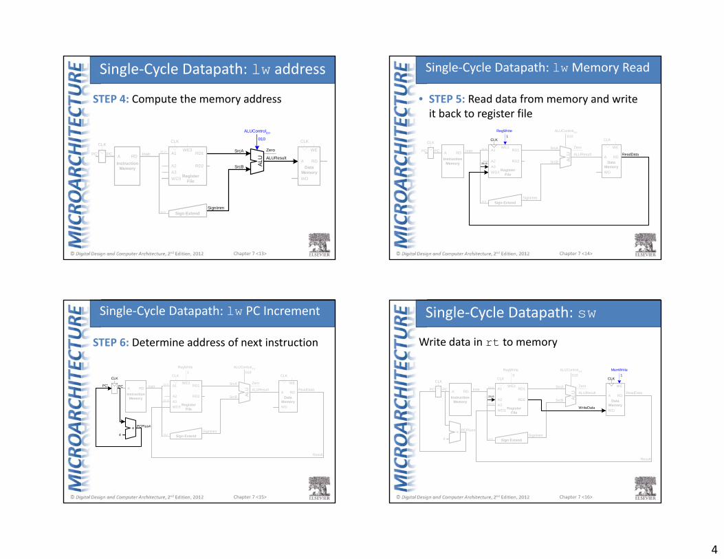
Chapter 7 <13>
STEP 4: Compute the memory address
SignImm
CLK
A RDInstruction
Memory
A1
A3WD3
RD2
RD1WE3
A2
CLK
Sign Extend
RegisterFile
A RDData
MemoryWD
WEPCPC' Instr 25:21
15:0
SrcB
ALUResult
SrcA Zero
CLK
ALUControl2:0
ALU
010
Single‐Cycle Datapath: lw address
Chapter 7 <14>
• STEP 5: Read data from memory and write it back to register file
A1
A3WD3
RD2
RD1WE3
A2
SignImm
CLK
A RDInstruction
Memory
CLK
Sign Extend
RegisterFile
A RDData
MemoryWD
WEPCPC' Instr 25:21
15:0
SrcB20:16
ALUResult ReadData
SrcA
RegWrite
Zero
CLK
ALUControl2:0
ALU
0101
Single‐Cycle Datapath: lwMemory Read
Chapter 7 <15>
STEP 6: Determine address of next instruction
SignImm
CLK
A RDInstruction
Memory
+
4
A1
A3WD3
RD2
RD1WE3
A2
CLK
Sign Extend
RegisterFile
A RDData
MemoryWD
WEPCPC' Instr 25:21
15:0
SrcB20:16
ALUResult ReadData
SrcA
PCPlus4
Result
RegWrite
Zero
CLK
ALUControl2:0
ALU
0101
Single‐Cycle Datapath: lw PC Increment
Chapter 7 <16>
Write data in rt to memory
SignImm
CLK
A RDInstruction
Memory
+
4
A1
A3WD3
RD2
RD1WE3
A2
CLK
Sign Extend
RegisterFile
A RDData
MemoryWD
WEPCPC' Instr 25:21
20:16
15:0
SrcB20:16
ALUResult ReadData
WriteData
SrcA
PCPlus4
Result
MemWriteRegWrite
Zero
CLK
ALUControl2:0
ALU
10100
Single‐Cycle Datapath: sw

5
Chapter 7 <17>
• Read from rs and rt• Write ALUResult to register file• Write to rd (instead of rt)
SignImm
CLK
A RDInstruction
Memory
+
4
A1
A3WD3
RD2
RD1WE3
A2
CLK
Sign Extend
RegisterFile
01
01
A RDData
MemoryWD
WE01
PCPC' Instr 25:21
20:16
15:0
SrcB
20:16
15:11
ALUResult ReadData
WriteData
SrcA
PCPlus4WriteReg4:0
Result
RegDst MemWrite MemtoRegALUSrcRegWrite
Zero
CLK
ALUControl2:0
ALU
0varies1 001
Single‐Cycle Datapath: R‐Type
Chapter 7 <18>
• Determine whether values in rs and rt are equal• Calculate branch target address:
BTA = (sign‐extended immediate << 2) + (PC+4)
SignImm
CLK
A RD
InstructionMemory
+
4
A1
A3WD3
RD2
RD1WE3
A2
CLK
Sign Extend
RegisterFile
01
01
A RDData
MemoryWD
WE01
PC01
PC' Instr 25:21
20:16
15:0
SrcB
20:16
15:11
<<2
+
ALUResult ReadData
WriteData
SrcA
PCPlus4
PCBranch
WriteReg4:0
Result
RegDst Branch MemWrite MemtoRegALUSrcRegWrite
Zero
PCSrc
CLK
ALUControl2:0
ALU
01100 x0x 1
Single‐Cycle Datapath: beq
Chapter 7 <19>
SignImm
CLK
A RDInstruction
Memory
+
4
A1
A3WD3
RD2
RD1WE3
A2
CLK
Sign Extend
RegisterFile
01
01
A RDData
MemoryWD
WE01
PC01
PC' Instr 25:21
20:16
15:0
5:0
SrcB
20:16
15:11
<<2
+
ALUResult ReadData
WriteData
SrcA
PCPlus4
PCBranch
WriteReg4:0
Result
31:26
RegDst
BranchMemWriteMemtoReg
ALUSrc
RegWrite
OpFunct
ControlUnit
Zero
PCSrc
CLK
ALUControl2:0
ALU
Single‐Cycle Processor
Chapter 7 <20>
RegDst
BranchMemWriteMemtoReg
ALUSrcOpcode5:0
ControlUnit
ALUControl2:0Funct5:0
MainDecoder
ALUOp1:0
ALUDecoder
RegWrite
Single‐Cycle Control

6
Chapter 7 <21>
ALU
N N
N3
A B
Y
F
F2:0 Function000 A & B001 A | B010 A + B011 not used100 A & ~B101 A | ~B110 A - B111 SLT
Review: ALU
Chapter 7 <22>
+
2 01
A B
Cout
Y3
01
F2
F1:0
[N-1] S
NN
N
N
N NNN
N
2Zero
Extend
Review: ALU
Chapter 7 <23>
ALUOp1:0 Meaning00 Add01 Subtract10 Look at Funct11 Not Used
ALUOp1:0 Funct ALUControl2:0
00 X 010 (Add)X1 X 110 (Subtract)1X 100000 (add) 010 (Add)1X 100010 (sub) 110 (Subtract)1X 100100 (and) 000 (And)1X 100101 (or) 001 (Or)1X 101010 (slt) 111 (SLT)
Control Unit: ALU Decoder
Chapter 7 <24>
Instruction Op5:0 RegWrite RegDst AluSrc Branch MemWrite MemtoReg ALUOp1:0
R-type 000000
lw 100011
sw 101011
beq 000100
SignImm
CLK
A RDInstruction
Memory
+4
A1
A3WD3
RD2
RD1WE3
A2
CLK
Sign Extend
RegisterFile
01
01
A RDData
MemoryWD
WE01
PC01
PC' Instr 25:21
20:16
15:0
5:0
SrcB
20:16
15:11
<<2
+
ALUResult ReadData
WriteData
SrcA
PCPlus4
PCBranch
WriteReg4:0
Result
31:26
RegDst
BranchMemWriteMemtoReg
ALUSrc
RegWrite
OpFunct
ControlUnit
Zero
PCSrc
CLK
ALUControl2:0
ALU
Control Unit Main Decoder

7
Chapter 7 <25>
Instruction Op5:0 RegWrite RegDst AluSrc Branch MemWrite MemtoReg ALUOp1:0
R-type 000000 1 1 0 0 0 0 10lw 100011 1 0 1 0 0 0 00sw 101011 0 X 1 0 1 X 00beq 000100 0 X 0 1 0 X 01
Control Unit: Main Decoder
Chapter 7 <26>
SignImm
CLK
A RDInstruction
Memory
+
4
A1
A3WD3
RD2
RD1WE3
A2
CLK
Sign Extend
RegisterFile
01
01
A RDData
MemoryWD
WE01
PC01
PC' Instr 25:21
20:16
15:0
5:0
SrcB
20:16
15:11
<<2
+
ALUResult ReadData
WriteData
SrcA
PCPlus4
PCBranch
WriteReg4:0
Result
31:26
RegDst
BranchMemWriteMemtoReg
ALUSrc
RegWrite
OpFunct
ControlUnit
Zero
PCSrc
CLK
ALUControl2:0
ALU
0010
01
0
0
1
0
Single‐Cycle Datapath: or
Chapter 7 <27>
SignImm
CLK
A RDInstruction
Memory
+
4
A1
A3WD3
RD2
RD1WE3
A2
CLK
Sign Extend
RegisterFile
01
01
A RDData
MemoryWD
WE01
PC01
PC' Instr 25:21
20:16
15:0
5:0
SrcB
20:16
15:11
<<2
+
ALUResult ReadData
WriteData
SrcA
PCPlus4
PCBranch
WriteReg4:0
Result
31:26
RegDst
BranchMemWriteMemtoReg
ALUSrc
RegWrite
OpFunct
ControlUnit
Zero
PCSrc
CLK
ALUControl2:0
ALU
No change to datapath
Extended Functionality: addi
Chapter 7 <28>
Instruction Op5:0 RegWrite RegDst AluSrc Branch MemWrite MemtoReg ALUOp1:0
R-type 000000 1 1 0 0 0 0 10
lw 100011 1 0 1 0 0 1 00
sw 101011 0 X 1 0 1 X 00
beq 000100 0 X 0 1 0 X 01
addi 001000
Control Unit: addi

8
Chapter 7 <29>
Instruction Op5:0 RegWrite RegDst AluSrc Branch MemWrite MemtoReg ALUOp1:0
R-type 000000 1 1 0 0 0 0 10
lw 100011 1 0 1 0 0 1 00
sw 101011 0 X 1 0 1 X 00
beq 000100 0 X 0 1 0 X 01
addi 001000 1 0 1 0 0 0 00
Control Unit: addi
Chapter 7 <30>
SignImm
CLK
A RDInstruction
Memory
+
4
A1
A3WD3
RD2
RD1WE3
A2
CLK
Sign Extend
RegisterFile
01
01
A RDData
MemoryWD
WE01
PC01
PC' Instr 25:21
20:16
15:0
5:0
SrcB
20:16
15:11
<<2
+
ALUResult ReadData
WriteData
SrcA
PCPlus4
PCBranch
WriteReg4:0
Result
31:26
RegDst
BranchMemWriteMemtoReg
ALUSrc
RegWrite
OpFunct
ControlUnit
Zero
PCSrc
CLK
ALUControl2:0
ALU
01
25:0 <<2
27:0 31:28
PCJump
Jump
Extended Functionality: j
Chapter 7 <31>
Instruction Op5:0 RegWrite RegDst AluSrc Branch MemWrite MemtoReg ALUOp1:0 Jump
R-type 000000 1 1 0 0 0 0 10 0
lw 100011 1 0 1 0 0 1 00 0
sw 101011 0 X 1 0 1 X 00 0
beq 000100 0 X 0 1 0 X 01 0
j 000100
Control Unit: Main Decoder
Chapter 7 <32>
Instruction Op5:0 RegWrite RegDst AluSrc Branch MemWrite MemtoReg ALUOp1:0 Jump
R-type 000000 1 1 0 0 0 0 10 0
lw 100011 1 0 1 0 0 1 00 0
sw 101011 0 X 1 0 1 X 00 0
beq 000100 0 X 0 1 0 X 01 0
j 000100 0 X X X 0 X XX 1
Control Unit: Main Decoder

9
Chapter 7 <33>
Program Execution Time = (#instructions)(cycles/instruction)(seconds/cycle)= # instructions x CPI x TC
Review: Processor Performance
Chapter 7 <34>
SignImm
CLK
A RDInstruction
Memory
+
4
A1
A3WD3
RD2
RD1WE3
A2
CLK
Sign Extend
RegisterFile
01
01
A RDData
MemoryWD
WE01
PC01
PC' Instr 25:21
20:16
15:0
5:0
SrcB
20:16
15:11
<<2
+
ALUResult ReadData
WriteData
SrcA
PCPlus4
PCBranch
WriteReg4:0
Result
31:26
RegDst
BranchMemWriteMemtoReg
ALUSrc
RegWrite
OpFunct
ControlUnit
Zero
PCSrc
CLK
ALUControl2:0
ALU1
0100
1
0
1
0 0
TC limited by critical path (lw)
Single‐Cycle Performance
Chapter 7 <35>
• Single-cycle critical path:Tc = tpcq_PC + tmem + max(tRFread, tsext + tmux) + tALU + tmem + tmux + tRFsetup
• Typically, limiting paths are: – memory, ALU, register file – Tc = tpcq_PC + 2tmem + tRFread + tmux + tALU + tRFsetup
Single‐Cycle Performance
Chapter 7 <36>
Element Parameter Delay (ps)Register clock-to-Q tpcq_PC 30
Register setup tsetup 20
Multiplexer tmux 25
ALU tALU 200
Memory read tmem 250
Register file read tRFread 150
Register file setup tRFsetup 20
Tc = ?
Single‐Cycle Performance Example

10
Chapter 7 <37>
Element Parameter Delay (ps)Register clock-to-Q tpcq_PC 30
Register setup tsetup 20
Multiplexer tmux 25
ALU tALU 200
Memory read tmem 250
Register file read tRFread 150
Register file setup tRFsetup 20
Tc = tpcq_PC + 2tmem + tRFread + tmux + tALU + tRFsetup= [30 + 2(250) + 150 + 25 + 200 + 20] ps= 925 ps
Single‐Cycle Performance Example
Chapter 7 <38>
Program with 100 billion instructions:
Execution Time = # instructions x CPI x TC= (100 × 109)(1)(925 × 10-12 s)= 92.5 seconds
Single‐Cycle Performance Example
Chapter 7 <39>
• Single‐cycle:+ simple‐ cycle time limited by longest instruction (lw)‐ 2 adders/ALUs & 2 memories
• Multicycle:+ higher clock speed+ simpler instructions run faster+ reuse expensive hardware on multiple cycles‐ sequencing overhead paid many times
• Same design steps: datapath & control
Multicycle MIPS Processor
Chapter 7 <40>
CLK
ARD
Instr / DataMemory
A1
A3
WD3
RD2RD1
WE3
A2
CLK
RegisterFile
PCPC'
WD
WE
CLK
EN
• Replace Instruction and Data memories with a single unified memory – more realistic
Multicycle State Elements
11
Chapter 7 <41>
b
CLK
ARD
Instr / DataMemory
A1
A3
WD3
RD2RD1
WE3
A2
CLK
RegisterFile
PCPC' Instr
CLK
WD
WE
CLK
EN
IRWrite
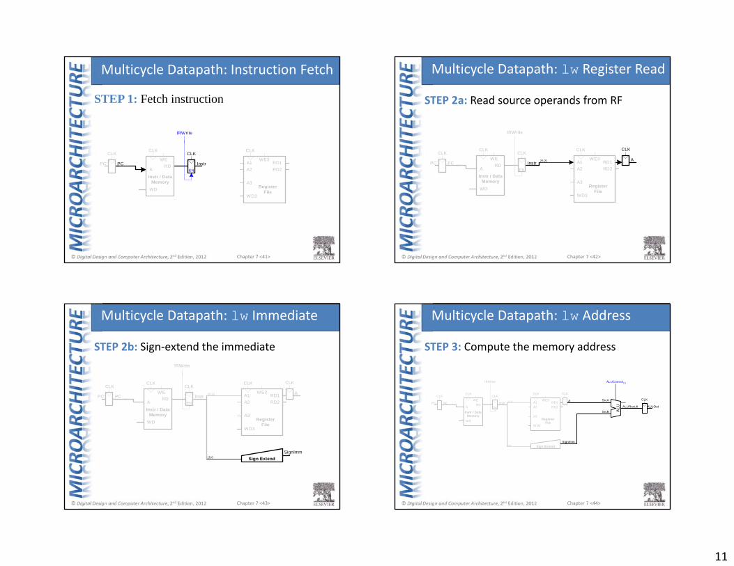
STEP 1: Fetch instruction
Multicycle Datapath: Instruction Fetch
Chapter 7 <42>
b
CLK
ARD
Instr / DataMemory
A1
A3
WD3
RD2RD1
WE3
A2
CLK
RegisterFile
PCPC' Instr 25:21
CLK
WD
WE
CLK CLK
A
EN
IRWrite
Multicycle Datapath: lw Register Read
STEP 2a: Read source operands from RF
Chapter 7 <43>
SignImm
b
CLK
ARD
Instr / DataMemory
A1
A3
WD3
RD2RD1
WE3
A2
CLK
Sign Extend
RegisterFile
PCPC' Instr 25:21
15:0
CLK
WD
WE
CLK CLK
A
EN
IRWrite
Multicycle Datapath: lw Immediate
STEP 2b: Sign‐extend the immediate
Chapter 7 <44>
SignImm
b
CLK
ARD
Instr / DataMemory
A1
A3
WD3
RD2RD1
WE3
A2
CLK
Sign Extend
RegisterFile
PCPC' Instr 25:21
15:0
SrcB
ALUResult
SrcA
ALUOut
CLK
ALUControl2:0
ALU
WD
WE
CLK CLK
A CLK
EN
IRWrite
Multicycle Datapath: lw Address
STEP 3: Compute the memory address

12
Chapter 7 <45>
SignImm
b
CLK
ARD
Instr / DataMemory
A1
A3
WD3
RD2RD1
WE3
A2
CLK
Sign Extend
RegisterFile
PCPC' Instr 25:21
15:0
SrcB
ALUResult
SrcA
ALUOut
CLK
ALUControl2:0
ALU
WD
WE
CLK
Adr
Data
CLK
CLK
A CLK
EN
IRWriteIorD
01
Multicycle Datapath: lwMemory Read
STEP 4: Read data from memory
Chapter 7 <46>
SignImm
b
CLK
ARD
Instr / DataMemory
A1
A3
WD3
RD2RD1
WE3
A2
CLK
Sign Extend
RegisterFile
PCPC' Instr 25:21
15:0
SrcB20:16
ALUResult
SrcA
ALUOut
RegWrite
CLK
ALUControl2:0
ALU
WD
WE
CLK
Adr
Data
CLK
CLK
A CLK
EN
IRWriteIorD
01
Multicycle Datapath: lwWrite Register
STEP 5:Write data back to register file
Chapter 7 <47>
PCWrite
SignImm
b
CLK
ARD
Instr / DataMemory
A1
A3
WD3
RD2RD1
WE3
A2
CLK
Sign Extend
RegisterFile
01PCPC' Instr 25:21
15:0
SrcB20:16
ALUResult
SrcA
ALUOut
ALUSrcARegWrite
CLK
ALUControl2:0
ALU
WD
WE
CLK
Adr
Data
CLK
CLK
A
00011011
4
CLK
ENEN
ALUSrcB1:0IRWriteIorD
01
Multicycle Datapath: Increment PC
STEP 6: Increment PC
Chapter 7 <48>
SignImm
b
CLK
ARD
Instr / DataMemory
A1
A3
WD3
RD2RD1
WE3
A2
CLK
Sign Extend
RegisterFile
01PC 0
1
PC' Instr 25:21
20:16
15:0
SrcB20:16
ALUResult
SrcA
ALUOut
MemWrite ALUSrcARegWrite
CLK
ALUControl2:0
ALU
WD
WE
CLK
Adr
Data
CLK
CLK
A
00011011
4
CLK
ENEN
ALUSrcB1:0IRWriteIorDPCWrite
B
Write data in rt to memory
Multicycle Datapath: sw

13
Chapter 7 <49>
01
SignImm
b
CLK
ARD
Instr / DataMemory
A1
A3
WD3
RD2RD1
WE3
A2
CLK
Sign Extend
RegisterFile
01
01PC 0
1
PC' Instr 25:21
20:16
15:0
SrcB20:16
15:11
ALUResult
SrcA
ALUOut
RegDstMemWrite MemtoReg ALUSrcARegWrite
CLK
ALUControl2:0
ALU
WD
WE
CLK
Adr
Data
CLK
CLK
AB 00
011011
4
CLK
ENEN
ALUSrcB1:0IRWriteIorDPCWrite
• Read from rs and rt• Write ALUResult to register file• Write to rd (instead of rt)
Multicycle Datapath: R‐Type
Chapter 7 <50>
SignImm
b
CLK
ARD
Instr / DataMemory
A1
A3
WD3
RD2RD1
WE3
A2
CLK
Sign Extend
RegisterFile
01
01 0
1
PC 01
PC' Instr 25:21
20:16
15:0
SrcB20:16
15:11
<<2
ALUResult
SrcA
ALUOut
RegDst BranchMemWrite MemtoReg ALUSrcARegWrite
Zero
PCSrc
CLK
ALUControl2:0
ALU
WD
WE
CLK
Adr
01
Data
CLK
CLK
AB 00
011011
4
CLK
ENEN
ALUSrcB1:0IRWriteIorD PCWrite
PCEn
• rs == rt?• BTA = (sign-extended immediate << 2) + (PC+4)
Multicycle Datapath: beq
Chapter 7 <51>
SignImm
CLK
ARD
Instr / DataMemory
A1
A3
WD3
RD2RD1
WE3
A2
CLK
Sign Extend
RegisterFile
01
01 0
1
PC 01
PC' Instr 25:21
20:16
15:0
5:0
SrcB20:16
15:11
<<2
ALUResult
SrcA
ALUOut
31:26
RegD
st
Branch
MemWrite
Mem
toReg
ALUSrcARegWrite
OpFunct
ControlUnit
Zero
PCSrc
CLK
CLK
ALUControl2:0
ALU
WD
WE
CLK
Adr
01
Data
CLK
CLK
AB 00
011011
4
CLK
ENEN
ALUSrcB1:0IRWrite
IorD
PCWritePCEn
Multicycle Processor
Chapter 7 <52>
ALUSrcA
PCSrc
Branch
ALUSrcB1:0
Opcode5:0
ControlUnit
ALUControl2:0Funct5:0
MainController
(FSM)
ALUOp1:0
ALUDecoder
RegWrite
PCWrite
IorD
MemWriteIRWrite
RegDstMemtoReg
RegisterEnables
MultiplexerSelects
Multicycle Control

14
Chapter 7 <53>
SignImm
CLK
ARD
Instr / DataMemory
A1
A3
WD3
RD2RD1
WE3
A2
CLK
Sign Extend
RegisterFile
01
01 0
1
PC 01
PC' Instr 25:21
20:16
15:0
5:0
SrcB20:16
15:11
<<2
ALUResult
SrcA
ALUOut
31:26
RegD
st
Branch
MemWrite
Mem
toReg
ALUSrcARegWrite
OpFunct
ControlUnit
Zero
PCSrc
CLK
CLK
ALUControl2:0
ALU
WD
WE
CLK
Adr
01
Data
CLK
CLK
AB 00
011011
4
CLK
ENEN
ALUSrcB1:0IRWrite
IorD
PCWritePCEn
0
1 1
0
X
X
00
01
0100
10
Reset
S0: Fetch
Main Controller FSM: Fetch
Chapter 7 <54>
SignImm
CLK
ARD
Instr / DataMemory
A1
A3
WD3
RD2RD1
WE3
A2
CLK
Sign Extend
RegisterFile
01
01 0
1
PC 01
PC' Instr 25:21
20:16
15:0
5:0
SrcB20:16
15:11
<<2
ALUResult
SrcA
ALUOut
31:26
RegD
st
Branch
MemWrite
Mem
toReg
ALUSrcARegWrite
OpFunct
ControlUnit
Zero
PCSrc
CLK
CLK
ALUControl2:0
ALU
WD
WE
CLK
Adr
01
Data
CLK
CLK
AB 00
011011
4
CLK
ENEN
ALUSrcB1:0IRWrite
IorD
PCWritePCEn
0
1 1
0
X
X
00
01
0100
10
IorD = 0AluSrcA = 0
ALUSrcB = 01ALUOp = 00PCSrc = 0
IRWritePCWrite
Reset
S0: Fetch
Main Controller FSM: Fetch
Chapter 7 <55>
IorD = 0AluSrcA = 0
ALUSrcB = 01ALUOp = 00PCSrc = 0
IRWritePCWrite
Reset
S0: Fetch S1: Decode
SignImm
CLK
ARD
Instr / DataMemory
A1
A3
WD3
RD2RD1
WE3
A2
CLK
Sign Extend
RegisterFile
01
01 0
1
PC 01
PC' Instr 25:21
20:16
15:0
5:0
SrcB20:16
15:11
<<2
ALUResult
SrcA
ALUOut
31:26
RegD
st
Branch
MemWrite
Mem
toReg
ALUSrcARegWrite
OpFunct
ControlUnit
Zero
PCSrc
CLK
CLK
ALUControl2:0
ALU
WD
WE
CLK
Adr
01
Data
CLK
CLK
AB 00
011011
4
CLK
ENEN
ALUSrcB1:0IRWrite
IorD
PCWritePCEn
X
0 0
0
X
X
0X
XX
XXXX
00
Main Controller FSM: Decode
Chapter 7 <56>
IorD = 0AluSrcA = 0
ALUSrcB = 01ALUOp = 00PCSrc = 0
IRWritePCWrite
Reset
S0: Fetch
S2: MemAdr
S1: Decode
Op = LWor
Op = SW
SignImm
CLK
ARD
Instr / DataMemory
A1
A3
WD3
RD2RD1
WE3
A2
CLK
Sign Extend
RegisterFile
01
01 0
1
PC 01
PC' Instr 25:21
20:16
15:0
5:0
SrcB20:16
15:11
<<2
ALUResult
SrcA
ALUOut
31:26
RegD
st
Branch
MemWrite
Mem
toReg
ALUSrcARegWrite
OpFunct
ControlUnit
Zero
PCSrc
CLK
CLK
ALUControl2:0
ALU
WD
WE
CLK
Adr
01
Data
CLK
CLK
AB 00
011011
4
CLK
ENEN
ALUSrcB1:0IRWrite
IorD
PCWritePCEn
X
0 0
0
X
X
01
10
010X
00
Main Controller FSM: Address

15
Chapter 7 <57>
IorD = 0AluSrcA = 0
ALUSrcB = 01ALUOp = 00PCSrc = 0
IRWritePCWrite
ALUSrcA = 1ALUSrcB = 10ALUOp = 00
Reset
S0: Fetch
S2: MemAdr
S1: Decode
Op = LWor
Op = SW
SignImm
CLK
ARD
Instr / DataMemory
A1
A3
WD3
RD2RD1
WE3
A2
CLK
Sign Extend
RegisterFile
01
01 0
1
PC 01
PC' Instr 25:21
20:16
15:0
5:0
SrcB20:16
15:11
<<2
ALUResult
SrcA
ALUOut
31:26
RegD
st
Branch
MemWrite
Mem
toReg
ALUSrcARegWrite
OpFunct
ControlUnit
Zero
PCSrc
CLK
CLK
ALUControl2:0
ALU
WD
WE
CLK
Adr
01
Data
CLK
CLK
AB 00
011011
4
CLK
ENEN
ALUSrcB1:0IRWrite
IorD
PCWritePCEn
X
0 0
0
X
X
01
10
010X
00
Main Controller FSM: Address
Chapter 7 <58>
IorD = 0AluSrcA = 0
ALUSrcB = 01ALUOp = 00PCSrc = 0
IRWritePCWrite
ALUSrcA = 1ALUSrcB = 10ALUOp = 00
IorD = 1
Reset
S0: Fetch
S2: MemAdr
S1: Decode
S3: MemRead
Op = LWor
Op = SW
Op = LW
RegDst = 0MemtoReg = 1
RegWrite
S4: MemWriteback
Main Controller FSM: lw
Chapter 7 <59>
IorD = 0AluSrcA = 0
ALUSrcB = 01ALUOp = 00PCSrc = 0
IRWritePCWrite
ALUSrcA = 1ALUSrcB = 10ALUOp = 00
IorD = 1 IorD = 1MemWrite
Reset
S0: Fetch
S2: MemAdr
S1: Decode
S3: MemReadS5: MemWrite
Op = LWor
Op = SW
Op = LWOp = SW
RegDst = 0MemtoReg = 1
RegWrite
S4: MemWriteback
Main Controller FSM: sw
Chapter 7 <60>
IorD = 0AluSrcA = 0
ALUSrcB = 01ALUOp = 00PCSrc = 0
IRWritePCWrite
ALUSrcA = 1ALUSrcB = 10ALUOp = 00
IorD = 1RegDst = 1
MemtoReg = 0RegWrite
IorD = 1MemWrite
ALUSrcA = 1ALUSrcB = 00ALUOp = 10
Reset
S0: Fetch
S2: MemAdr
S1: Decode
S3: MemReadS5: MemWrite
S6: Execute
S7: ALUWriteback
Op = LWor
Op = SWOp = R-type
Op = LWOp = SW
RegDst = 0MemtoReg = 1
RegWrite
S4: MemWriteback
Main Controller FSM: R‐Type

16
Chapter 7 <61>
IorD = 0AluSrcA = 0
ALUSrcB = 01ALUOp = 00PCSrc = 0
IRWritePCWrite
ALUSrcA = 0ALUSrcB = 11ALUOp = 00
ALUSrcA = 1ALUSrcB = 10ALUOp = 00
IorD = 1RegDst = 1
MemtoReg = 0RegWrite
IorD = 1MemWrite
ALUSrcA = 1ALUSrcB = 00ALUOp = 10
ALUSrcA = 1ALUSrcB = 00ALUOp = 01PCSrc = 1
Branch
Reset
S0: Fetch
S2: MemAdr
S1: Decode
S3: MemReadS5: MemWrite
S6: Execute
S7: ALUWriteback
S8: Branch
Op = LWor
Op = SWOp = R-type
Op = BEQ
Op = LWOp = SW
RegDst = 0MemtoReg = 1
RegWrite
S4: MemWriteback
Main Controller FSM: beq
Chapter 7 <62>
IorD = 0AluSrcA = 0
ALUSrcB = 01ALUOp = 00PCSrc = 0
IRWritePCWrite
ALUSrcA = 0ALUSrcB = 11ALUOp = 00
ALUSrcA = 1ALUSrcB = 10ALUOp = 00
IorD = 1RegDst = 1
MemtoReg = 0RegWrite
IorD = 1MemWrite
ALUSrcA = 1ALUSrcB = 00ALUOp = 10
ALUSrcA = 1ALUSrcB = 00ALUOp = 01PCSrc = 1
Branch
Reset
S0: Fetch
S2: MemAdr
S1: Decode
S3: MemReadS5: MemWrite
S6: Execute
S7: ALUWriteback
S8: Branch
Op = LWor
Op = SWOp = R-type
Op = BEQ
Op = LWOp = SW
RegDst = 0MemtoReg = 1
RegWrite
S4: MemWriteback
Multicycle Controller FSM
Chapter 7 <63>
IorD = 0AluSrcA = 0
ALUSrcB = 01ALUOp = 00PCSrc = 0
IRWritePCWrite
ALUSrcA = 0ALUSrcB = 11ALUOp = 00
ALUSrcA = 1ALUSrcB = 10ALUOp = 00
IorD = 1RegDst = 1
MemtoReg = 0RegWrite
IorD = 1MemWrite
ALUSrcA = 1ALUSrcB = 00ALUOp = 10
ALUSrcA = 1ALUSrcB = 00ALUOp = 01PCSrc = 1
Branch
Reset
S0: Fetch
S2: MemAdr
S1: Decode
S3: MemReadS5: MemWrite
S6: Execute
S7: ALUWriteback
S8: Branch
Op = LWor
Op = SWOp = R-type
Op = BEQ
Op = LWOp = SW
RegDst = 0MemtoReg = 1
RegWrite
S4: MemWriteback
Op = ADDI
S9: ADDIExecute
S10: ADDIWriteback
Extended Functionality: addi
Chapter 7 <64>
IorD = 0AluSrcA = 0
ALUSrcB = 01ALUOp = 00PCSrc = 0
IRWritePCWrite
ALUSrcA = 0ALUSrcB = 11ALUOp = 00
ALUSrcA = 1ALUSrcB = 10ALUOp = 00
IorD = 1RegDst = 1
MemtoReg = 0RegWrite
IorD = 1MemWrite
ALUSrcA = 1ALUSrcB = 00ALUOp = 10
ALUSrcA = 1ALUSrcB = 00ALUOp = 01PCSrc = 1
Branch
Reset
S0: Fetch
S2: MemAdr
S1: Decode
S3: MemReadS5: MemWrite
S6: Execute
S7: ALUWriteback
S8: Branch
Op = LWor
Op = SWOp = R-type
Op = BEQ
Op = LWOp = SW
RegDst = 0MemtoReg = 1
RegWrite
S4: MemWriteback
ALUSrcA = 1ALUSrcB = 10ALUOp = 00
RegDst = 0MemtoReg = 0
RegWrite
Op = ADDI
S9: ADDIExecute
S10: ADDIWriteback
Main Controller FSM: addi

17
Chapter 7 <65>
SignImm
CLK
ARD
Instr / DataMemory
A1
A3
WD3
RD2RD1
WE3
A2
CLK
Sign Extend
RegisterFile
01
01PC 0
1
PC' Instr 25:21
20:16
15:0
SrcB20:16
15:11
<<2
ALUResult
SrcA
ALUOut
RegDst BranchMemWrite MemtoReg ALUSrcARegWrite
Zero
PCSrc1:0
CLK
ALUControl2:0
ALU
WD
WE
CLK
Adr
01
Data
CLK
CLK
AB 00
011011
4
CLK
ENEN
ALUSrcB1:0IRWriteIorD PCWrite
PCEn
000110
<<2
25:0 (jump)
31:28
27:0
PCJump
Extended Functionality: j
Chapter 7 <66>
IorD = 0AluSrcA = 0
ALUSrcB = 01ALUOp = 00PCSrc = 00
IRWritePCWrite
ALUSrcA = 0ALUSrcB = 11ALUOp = 00
ALUSrcA = 1ALUSrcB = 10ALUOp = 00
IorD = 1RegDst = 1
MemtoReg = 0RegWrite
IorD = 1MemWrite
ALUSrcA = 1ALUSrcB = 00ALUOp = 10
ALUSrcA = 1ALUSrcB = 00ALUOp = 01PCSrc = 01
Branch
Reset
S0: Fetch
S2: MemAdr
S1: Decode
S3: MemReadS5: MemWrite
S6: Execute
S7: ALUWriteback
S8: Branch
Op = LWor
Op = SWOp = R-type
Op = BEQ
Op = LWOp = SW
RegDst = 0MemtoReg = 1
RegWrite
S4: MemWriteback
ALUSrcA = 1ALUSrcB = 10ALUOp = 00
RegDst = 0MemtoReg = 0
RegWrite
Op = ADDI
S9: ADDIExecute
S10: ADDIWriteback
Op = J
S11: Jump
Main Controller FSM: j
Chapter 7 <67>
IorD = 0AluSrcA = 0
ALUSrcB = 01ALUOp = 00PCSrc = 00
IRWritePCWrite
ALUSrcA = 0ALUSrcB = 11ALUOp = 00
ALUSrcA = 1ALUSrcB = 10ALUOp = 00
IorD = 1RegDst = 1
MemtoReg = 0RegWrite
IorD = 1MemWrite
ALUSrcA = 1ALUSrcB = 00ALUOp = 10
ALUSrcA = 1ALUSrcB = 00ALUOp = 01PCSrc = 01
Branch
Reset
S0: Fetch
S2: MemAdr
S1: Decode
S3: MemReadS5: MemWrite
S6: Execute
S7: ALUWriteback
S8: Branch
Op = LWor
Op = SWOp = R-type
Op = BEQ
Op = LWOp = SW
RegDst = 0MemtoReg = 1
RegWrite
S4: MemWriteback
ALUSrcA = 1ALUSrcB = 10ALUOp = 00
RegDst = 0MemtoReg = 0
RegWrite
Op = ADDI
S9: ADDIExecute
S10: ADDIWriteback
PCSrc = 10PCWrite
Op = J
S11: Jump
Main Controller FSM: j
Chapter 7 <68>
• Instructions take different number of cycles:– 3 cycles: beq, j– 4 cycles: R-Type, sw, addi– 5 cycles: lw
• CPI is weighted average• SPECINT2000 benchmark:
– 25% loads– 10% stores– 11% branches– 2% jumps– 52% R-type
Average CPI = (0.11 + 0.2)(3) + (0.52 + 0.10)(4) + (0.25)(5) = 4.12
Multicycle Processor Performance

18
Chapter 7 <69>
SignImm
CLK
ARD
Instr / DataMemory
A1
A3
WD3
RD2RD1
WE3
A2
CLK
Sign Extend
RegisterFile
01
01 0
1
PC 01
PC' Instr 25:21
20:16
15:0
5:0
SrcB20:16
15:11
<<2
ALUResult
SrcA
ALUOut
31:26
RegD
st
Branch
MemWrite
Mem
toReg
ALUSrcARegWrite
OpFunct
ControlUnit
Zero
PCSrc
CLK
CLK
ALUControl2:0
ALU
WD
WE
CLK
Adr
01
Data
CLK
CLK
AB 00
011011
4
CLK
ENEN
ALUSrcB1:0IRWrite
IorD
PCWritePCEn
Multicycle critical path:Tc = tpcq + tmux + max(tALU + tmux, tmem) + tsetup
Multicycle Processor Performance
Chapter 7 <70>
Element Parameter Delay (ps)Register clock-to-Q tpcq_PC 30
Register setup tsetup 20
Multiplexer tmux 25
ALU tALU 200
Memory read tmem 250
Register file read tRFread 150
Register file setup tRFsetup 20
Tc = ?
Multicycle Performance Example
Chapter 7 <71>
Element Parameter Delay (ps)Register clock-to-Q tpcq_PC 30
Register setup tsetup 20
Multiplexer tmux 25
ALU tALU 200
Memory read tmem 250
Register file read tRFread 150
Register file setup tRFsetup 20
Tc = tpcq_PC + tmux + max(tALU + tmux, tmem) + tsetup= tpcq_PC + tmux + tmem + tsetup= [30 + 25 + 250 + 20] ps= 325 ps
Multicycle Performance Example
Chapter 7 <72>
• For a program with 100 billion instructions executing on a multicycle MIPS processor
– CPI = 4.12– Tc = 325 ps
Execution Time =
Chapter 7 :: Topics

19
Chapter 7 <73>
• For a program with 100 billion instructions executing on a multicycle MIPS processor
– CPI = 4.12– Tc = 325 ps
Execution Time = (# instructions) × CPI × Tc= (100 × 109)(4.12)(325 × 10-12)= 133.9 seconds
• This is slower than the single-cycle processor (92.5 seconds). Why?
Chapter 7 <74>
Program with 100 billion instructions
Execution Time = (# instructions) × CPI × Tc
= (100 × 109)(4.12)(325 × 10-12)= 133.9 seconds
This is slower than the single-cycle processor (92.5 seconds). Why?– Not all steps same length– Sequencing overhead for each step (tpcq + tsetup= 50 ps)
Multicycle Performance Example
Chapter 7 <75>
SignImm
CLK
A RD
InstructionMemory
+
4
A1
A3WD3
RD2
RD1WE3
A2
CLK
Sign Extend
RegisterFile
01
01
A RDData
MemoryWD
WE01
PC01 PC' Instr 25:21
20:16
15:0
5:0
SrcB
20:16
15:11
<<2
+
ALUResult ReadData
WriteData
SrcA
PCPlus4
PCBranch
WriteReg4:0
Result
31:26
RegDst
BranchMemWriteMemtoReg
ALUSrc
RegWrite
OpFunct
ControlUnit
Zero
PCSrc
CLK
ALUControl2:0
ALU
01
25:0 <<2
27:0 31:28
PCJump
Jump
Review: Single‐Cycle Processor
Chapter 7 <76>
ImmExt
CLK
ARD
Instr / DataMemory
A1
A3
WD3
RD2RD1
WE3
A2
CLK
Sign Extend
RegisterFile
01
01PC 0
1
PC' Instr 25:21
20:16
15:0
SrcB20:16
15:11
<<2
ALUResult
SrcA
ALUOut
ZeroCLK
ALU
WD
WE
CLK
Adr
01
Data
CLK
CLK
AB 00
011011
4
CLK
ENEN000110
<<2
25:0 (Addr)
31:28
27:0
PCJump
5:0
31:26
Branch
MemWrite
ALUSrcARegWrite
OpFunct
ControlUnit
PCSrc
CLK
ALUControl2:0
ALUSrcB1:0IRWrite
IorD
PCWritePCEn
RegD
st
Mem
toReg
Review: Multicycle Processor

20
Chapter 7 <77>
• Temporal parallelism• Divide single-cycle processor into 5 stages:
– Fetch– Decode– Execute– Memory– Writeback
• Add pipeline registers between stages
Pipelined MIPS Processor
Chapter 7 <78>
Time (ps)Instr
FetchInstruction
DecodeRead Reg
ExecuteALU
MemoryRead / Write
WriteReg1
2
0 100 200 300 400 500 600 700 800 900 1100 1200 1300 1400 1500 1600 1700 1800 19001000
Instr
1
2
3
FetchInstruction
DecodeRead Reg
ExecuteALU
MemoryRead / Write
WriteReg
FetchInstruction
DecodeRead Reg
ExecuteALU
MemoryRead/Write
WriteReg
FetchInstruction
DecodeRead Reg
ExecuteALU
MemoryRead/Write
WriteReg
FetchInstruction
DecodeRead Reg
ExecuteALU
MemoryRead/Write
WriteReg
Single-Cycle
Pipelined
Single‐Cycle vs. Pipelined
Chapter 7 <79>
Time (cycles)
lw $s2, 40($0) RF 40
$0RF
$s2+ DM
RF $t2
$t1RF
$s3+ DM
RF $s5
$s1RF
$s4- DM
RF $t6
$t5RF
$s5& DM
RF 20
$s1RF
$s6+ DM
RF $t4
$t3RF
$s7| DM
add $s3, $t1, $t2
sub $s4, $s1, $s5
and $s5, $t5, $t6
sw $s6, 20($s1)
or $s7, $t3, $t4
1 2 3 4 5 6 7 8 9 10
add
IM
IM
IM
IM
IM
IM lw
sub
and
sw
or
Pipelined Processor Abstraction
Chapter 7 <80>
SignImmE
CLK
A RDInstruction
Memory
+4
A1
A3WD3
RD2
RD1WE3
A2
CLK
Sign Extend
RegisterFile
01
01
A RDData
MemoryWD
WE01
PCF01
PC' InstrD 25:21
20:16
15:0
SrcBE
20:16
15:11
RtE
RdE
<<2
+
ALUOutM
ALUOutW
ReadDataW
WriteDataE WriteDataM
SrcAE
PCPlus4D
PCBranchM
ResultW
PCPlus4EPCPlus4F
ZeroM
CLK CLK
ALU
WriteRegE4:0
CLKCLK
CLK
SignImm
CLK
A RDInstruction
Memory
+
4
A1
A3WD3
RD2
RD1WE3
A2
CLK
Sign Extend
RegisterFile
01
01
A RDData
MemoryWD
WE01
PC01
PC' Instr 25:21
20:16
15:0
SrcB
20:16
15:11
<<2
+
ALUResult ReadData
WriteData
SrcA
PCPlus4
PCBranch
WriteReg4:0
Result
Zero
CLK
ALU
Fetch Decode Execute Memory Writeback
Single‐Cycle & Pipelined Datapath

21
Chapter 7 <81>
SignImmE
CLK
A RDInstruction
Memory
+
4
A1
A3WD3
RD2
RD1WE3
A2
CLK
Sign Extend
RegisterFile
01
01
A RDData
MemoryWD
WE01
PCF01
PC' InstrD 25:21
20:16
15:0
SrcBE
20:16
15:11
RtE
RdE
<<2
+
ALUOutM
ALUOutW
ReadDataW
WriteDataE WriteDataM
SrcAE
PCPlus4D
PCBranchM
WriteRegM4:0
ResultW
PCPlus4EPCPlus4F
ZeroM
CLK CLK
WriteRegW4:0
ALU
WriteRegE4:0
CLKCLK
CLK
Fetch Decode Execute Memory Writeback
WriteReg must arrive at same time as Result
Corrected Pipelined Datapath
Chapter 7 <82>
SignImmE
CLK
A RDInstruction
Memory
+
4
A1
A3WD3
RD2
RD1WE3
A2
CLK
Sign Extend
RegisterFile
01
01
A RDData
MemoryWD
WE01
PCF01
PC' InstrD25:21
20:16
15:0
5:0
SrcBE
20:16
15:11
RtE
RdE
<<2
+
ALUOutM
ALUOutW
ReadDataW
WriteDataE WriteDataM
SrcAE
PCPlus4D
PCBranchM
WriteRegM4:0
ResultW
PCPlus4EPCPlus4F
31:26
RegDstD
BranchD
MemWriteD
MemtoRegD
ALUControlD
ALUSrcD
RegWriteD
Op
Funct
ControlUnit
ZeroM
PCSrcM
CLK CLK CLK
CLK CLK
WriteRegW4:0
ALUControlE2:0
ALU
RegWriteE RegWriteM RegWriteW
MemtoRegE MemtoRegM MemtoRegW
MemWriteE MemWriteM
BranchE BranchM
RegDstE
ALUSrcE
WriteRegE4:0
• Same control unit as single‐cycle processor• Control delayed to proper pipeline stage
Pipelined Processor Control
Chapter 7 <83>
• When an instruction depends on result from instruction that hasn’t completed
• Types:– Data hazard: register value not yet written back to register file
– Control hazard: next instruction not decided yet (caused by branches)
Pipeline Hazards
Chapter 7 <84>
Time (cycles)
add $s0, $s2, $s3 RF $s3
$s2RF
$s0+ DM
RF $s1
$s0RF
$t0& DM
RF $s0
$s4RF
$t1| DM
RF $s5
$s0RF
$t2- DM
and $t0, $s0, $s1
or $t1, $s4, $s0
sub $t2, $s0, $s5
1 2 3 4 5 6 7 8
and
IM
IM
IM
IM add
or
sub
Data Hazard

22
Chapter 7 <85>
• Insert nops in code at compile time• Rearrange code at compile time• Forward data at run time• Stall the processor at run time
Handling Data Hazards
Chapter 7 <86>
Time (cycles)
add $s0, $s2, $s3 RF $s3
$s2RF
$s0+ DM
RF $s1
$s0RF
$t0& DM
RF $s0
$s4RF
$t1| DM
RF $s5
$s0RF
$t2- DM
and $t0, $s0, $s1
or $t1, $s4, $s0
sub $t2, $s0, $s5
1 2 3 4 5 6 7 8
and
IM
IM
IM
IM add
or
sub
nop
nop
RF RFDMnopIM
RF RFDMnopIM
9 10
• Insert enough nops for result to be ready• Or move independent useful instructions forward
Compile‐Time Hazard Elimination
Chapter 7 <87>
Time (cycles)
add $s0, $s2, $s3 RF $s3
$s2RF
$s0+ DM
RF $s1
$s0RF
$t0& DM
RF $s0
$s4RF
$t1| DM
RF $s5
$s0RF
$t2- DM
and $t0, $s0, $s1
or $t1, $s4, $s0
sub $t2, $s0, $s5
1 2 3 4 5 6 7 8
and
IM
IM
IM
IM add
or
sub
Data Forwarding
Chapter 7 <88>
SignImmE
CLK
A RDInstruction
Memory
+
4
A1
A3WD3
RD2
RD1WE3
A2
CLK
SignExtend
RegisterFile
01
01
A RDData
MemoryWD
WE
10
PCF01
PC' InstrD 25:21
20:16
15:0
5:0
SrcBE
25:21
15:11
RsE
RdE
<<2
+
ALUOutM
ALUOutW
ReadDataW
WriteDataE WriteDataM
SrcAE
PCPlus4D
PCBranchM
WriteRegM4:0
ResultW
PCPlus4F
31:26
RegDstD
BranchD
MemWriteD
MemtoRegD
ALUControlD2:0
ALUSrcD
RegWriteD
Op
Funct
ControlUnit
PCSrcM
CLK CLK CLK
CLK CLK
WriteRegW4:0
ALUControlE2:0
ALU
RegWriteE RegWriteM RegWriteW
MemtoRegE MemtoRegM MemtoRegW
MemWriteE MemWriteM
RegDstE
ALUSrcE
WriteRegE4:0
000110
000110
SignImmD
Forw
ardA
E
Forw
ardB
E
20:16 RtE
RsD
RdD
RtD
Reg
Writ
eM
Reg
Writ
eW
Hazard Unit
PCPlus4E
BranchE BranchM
ZeroM
Data Forwarding

23
Chapter 7 <89>
• Forward to Execute stage from either:– Memory stage or– Writeback stage
• Forwarding logic for ForwardAE:if ((rsE != 0) AND (rsE == WriteRegM) AND RegWriteM)
then ForwardAE = 10else if ((rsE != 0) AND (rsE == WriteRegW) AND RegWriteW)
then ForwardAE = 01else ForwardAE = 00
Forwarding logic for ForwardBE same, but replace rsE with rtE
Data Forwarding
Chapter 7 <90>
Time (cycles)
lw $s0, 40($0) RF 40
$0RF
$s0+ DM
RF $s1
$s0RF
$t0& DM
RF $s0
$s4RF
$t1| DM
RF $s5
$s0RF
$t2- DM
and $t0, $s0, $s1
or $t1, $s4, $s0
sub $t2, $s0, $s5
1 2 3 4 5 6 7 8
and
IM
IM
IM
IM lw
or
sub
Trouble!
Stalling
Chapter 7 <91>
Time (cycles)
lw $s0, 40($0) RF 40
$0RF
$s0+ DM
RF $s1
$s0RF
$t0& DM
RF $s0
$s4RF
$t1| DM
RF $s5
$s0RF
$t2- DM
and $t0, $s0, $s1
or $t1, $s4, $s0
sub $t2, $s0, $s5
1 2 3 4 5 6 7 8
and
IM
IM
IM
IM lw
or
sub
9
RF $s1
$s0
IM or
Stall
Stalling
Chapter 7 <92>
SignImmE
CLK
A RDInstruction
Memory
+
4
A1
A3WD3
RD2
RD1WE3
A2
CLK
SignExtend
RegisterFile
01
01
A RDData
MemoryWD
WE
10
PCF01
PC' InstrD 25:21
20:16
15:0
5:0
SrcBE
25:21
15:11
RsE
RdE
<<2
+
ALUOutM
ALUOutW
ReadDataW
WriteDataE WriteDataM
SrcAE
PCPlus4D
PCBranchM
WriteRegM4:0
ResultW
PCPlus4F
31:26
RegDstD
BranchD
MemWriteD
MemtoRegD
ALUControlD2:0
ALUSrcD
RegWriteD
Op
Funct
ControlUnit
PCSrcM
CLK CLK CLK
CLK CLK
WriteRegW4:0
ALUControlE2:0
ALU
RegWriteE RegWriteM RegWriteW
MemtoRegE MemtoRegM MemtoRegW
MemWriteE MemWriteM
RegDstE
ALUSrcE
WriteRegE4:0
000110
000110
SignImmD
Sta
llF
Sta
llD
Forw
ardA
E
Forw
ardB
E
20:16 RtE
RsD
RdD
RtD
Reg
Writ
eM
Reg
Writ
eW
Mem
toR
egE
Hazard Unit
Flus
hE
PCPlus4E
BranchE BranchM
ZeroM
EN
EN
CLR
Stalling Hardware

24
Chapter 7 <93>
lwstall =((rsD==rtE) OR (rtD==rtE)) AND MemtoRegE
StallF = StallD = FlushE = lwstall
Stalling Logic
Chapter 7 <94>
• beq: – branch not determined until 4th stage of pipeline– Instructions after branch fetched before branch occurs– These instructions must be flushed if branch happens
• Branch misprediction penalty– number of instruction flushed when branch is taken– May be reduced by determining branch earlier
Control Hazards
Chapter 7 <95>
SignImmE
CLK
A RDInstruction
Memory
+
4
A1
A3WD3
RD2
RD1WE3
A2
CLK
SignExtend
RegisterFile
01
01
A RDData
MemoryWD
WE
10
PCF01
PC' InstrD 25:21
20:16
15:0
5:0
SrcBE
25:21
15:11
RsE
RdE
<<2
+
ALUOutM
ALUOutW
ReadDataW
WriteDataE WriteDataM
SrcAE
PCPlus4D
PCBranchM
WriteRegM4:0
ResultW
PCPlus4F
31:26
RegDstD
BranchD
MemWriteD
MemtoRegD
ALUControlD2:0
ALUSrcD
RegWriteD
Op
Funct
ControlUnit
PCSrcM
CLK CLK CLK
CLK CLK
WriteRegW4:0
ALUControlE2:0
ALU
RegWriteE RegWriteM RegWriteW
MemtoRegE MemtoRegM MemtoRegW
MemWriteE MemWriteM
RegDstE
ALUSrcE
WriteRegE4:0
000110
000110
SignImmD
Stal
lF
Stal
lD
Forw
ardA
E
Forw
ardB
E
20:16 RtE
RsD
RdD
RtD
Reg
Writ
eM
Reg
Writ
eW
Mem
toR
egE
Hazard Unit
Flus
hE
PCPlus4E
BranchE BranchM
ZeroM
EN
EN
CLR
Control Hazards: Original Pipeline
Chapter 7 <96>
Time (cycles)
beq $t1, $t2, 40 RF $t2
$t1RF- DM
RF $s1
$s0RF& DM
RF $s0
$s4RF| DM
RF $s5
$s0RF- DM
and $t0, $s0, $s1
or $t1, $s4, $s0
sub $t2, $s0, $s5
1 2 3 4 5 6 7 8
and
IM
IM
IM
IM lw
or
sub
20
24
28
2C
30
...
...
9
Flushthese
instructions
64 slt $t3, $s2, $s3 RF $s3
$s2RF
$t3slt DMIM slt
Control Hazards

25
Chapter 7 <97>
EqualD
SignImmE
CLK
A RDInstruction
Memory
+
4
A1
A3WD3
RD2
RD1WE3
A2
CLK
SignExtend
RegisterFile
01
01
A RDData
MemoryWD
WE
10
PCF01
PC' InstrD 25:21
20:16
15:0
5:0
SrcBE
25:21
15:11
RsE
RdE
<<2
+
ALUOutM
ALUOutW
ReadDataW
WriteDataE WriteDataM
SrcAE
PCPlus4D
PCBranchD
WriteRegM4:0
ResultW
PCPlus4F
31:26
RegDstD
BranchD
MemWriteD
MemtoRegD
ALUControlD2:0
ALUSrcD
RegWriteD
Op
Funct
ControlUnit
PCSrcD
CLK CLK CLK
CLK CLK
WriteRegW4:0
ALUControlE2:0
ALU
RegWriteE RegWriteM RegWriteW
MemtoRegE MemtoRegM MemtoRegW
MemWriteE MemWriteM
RegDstE
ALUSrcE
WriteRegE4:0
000110
000110
=
SignImmD
Stal
lF
Stal
lD
Forw
ardA
E
Forw
ardB
E
20:16 RtE
RsD
RdE
RtD
Reg
Writ
eM
Reg
Writ
eW
Mem
toR
egE
Hazard Unit
Flus
hE
EN
EN
CLR
CLR
Introduced another data hazard in Decode stage
Early Branch Resolution
Chapter 7 <98>
Time (cycles)
beq $t1, $t2, 40 RF $t2
$t1RF- DM
RF $s1
$s0RF& DMand $t0, $s0, $s1
or $t1, $s4, $s0
sub $t2, $s0, $s5
1 2 3 4 5 6 7 8
andIM
IM lw20
24
28
2C
30
...
...
9
Flushthis
instruction
64 slt $t3, $s2, $s3 RF $s3
$s2RF
$t3slt DMIM slt
Early Branch Resolution
Chapter 7 <99>
EqualD
SignImmE
CLK
A RDInstruction
Memory
+
4
A1
A3WD3
RD2
RD1WE3
A2
CLK
SignExtend
RegisterFile
01
01
A RDData
MemoryWD
WE
10
PCF01
PC' InstrD 25:21
20:16
15:0
5:0
SrcBE
25:21
15:11
RsE
RdE
<<2
+
ALUOutM
ALUOutW
ReadDataW
WriteDataE WriteDataM
SrcAE
PCPlus4D
PCBranchD
WriteRegM4:0
ResultW
PCPlus4F
31:26
RegDstD
BranchD
MemWriteD
MemtoRegD
ALUControlD2:0
ALUSrcD
RegWriteD
Op
Funct
ControlUnit
PCSrcD
CLK CLK CLK
CLK CLK
WriteRegW4:0
ALUControlE2:0
ALU
RegWriteE RegWriteM RegWriteW
MemtoRegE MemtoRegM MemtoRegW
MemWriteE MemWriteM
RegDstE
ALUSrcE
WriteRegE4:0
000110
000110
01
01
=
SignImmD
Stal
lF
Stal
lD
Forw
ardA
E
Forw
ardB
E
Forw
ardA
D
Forw
ardB
D
20:16 RtE
RsD
RdD
RtD
Reg
Writ
eE
Reg
Writ
eM
Reg
Writ
eW
Mem
toR
egE
Bran
chD
Hazard Unit
Flus
hE
EN
EN
CLR
CLR
Handling Data & Control Hazards
Chapter 7 <100>
• Forwarding logic:ForwardAD = (rsD !=0) AND (rsD == WriteRegM) AND RegWriteM
ForwardBD = (rtD !=0) AND (rtD == WriteRegM) AND RegWriteM
• Stalling logic:branchstall = BranchD AND RegWriteE AND
(WriteRegE == rsD OR WriteRegE == rtD)
OR
BranchD AND MemtoRegM AND
(WriteRegM == rsD OR WriteRegM == rtD)
StallF = StallD = FlushE = lwstall OR branchstall
Control Forwarding & Stalling Logic

26
Chapter 7 <101>
• Guess whether branch will be taken– Backward branches are usually taken (loops)– Consider history to improve guess
• Good prediction reduces fraction of branches requiring a flush
Branch Prediction
Chapter 7 <102>
• SPECINT2000 benchmark:– 25% loads– 10% stores– 11% branches– 2% jumps– 52% R-type
• Suppose:– 40% of loads used by next instruction– 25% of branches mispredicted– All jumps flush next instruction
• What is the average CPI?
Pipelined Performance Example
Chapter 7 <103>
• SPECINT2000 benchmark:– 25% loads– 10% stores– 11% branches– 2% jumps– 52% R-type
• Suppose:– 40% of loads used by next instruction– 25% of branches mispredicted– All jumps flush next instruction
• What is the average CPI?– Load/Branch CPI = 1 when no stalling, 2 when stalling– CPIlw = 1(0.6) + 2(0.4) = 1.4– CPIbeq = 1(0.75) + 2(0.25) = 1.25
Average CPI = (0.25)(1.4) + (0.1)(1) + (0.11)(1.25) + (0.02)(2) + (0.52)(1)
= 1.15
Pipelined Performance Example
Chapter 7 <104>
• Pipelined processor critical path:Tc = max {
tpcq + tmem + tsetup2(tRFread + tmux + teq + tAND + tmux + tsetup )tpcq + tmux + tmux + tALU + tsetuptpcq + tmemwrite + tsetup2(tpcq + tmux + tRFwrite) }
Pipelined Performance

27
Chapter 7 <105>
Element Parameter Delay (ps)Register clock-to-Q tpcq_PC 30Register setup tsetup 20Multiplexer tmux 25ALU tALU 200Memory read tmem 250Register file read tRFread 150Register file setup tRFsetup 20Equality comparator teq 40AND gate tAND 15Memory write Tmemwrite 220Register file write tRFwrite 100 ps
Tc = 2(tRFread + tmux + teq + tAND + tmux + tsetup )= 2[150 + 25 + 40 + 15 + 25 + 20] ps = 550 ps
Pipelined Performance Example
Chapter 7 <106>
Program with 100 billion instructionsExecution Time = (# instructions) × CPI × Tc
= (100 × 109)(1.15)(550 × 10-12)= 63 seconds
Pipelined Performance Example
Chapter 7 <107>
Processor
Execution Time(seconds)
Speedup(single-cycle as baseline)
Single-cycle 92.5 1
Multicycle 133 0.70
Pipelined 63 1.47
Processor Performance Comparison
Chapter 7 <108>
• Unscheduled function call to exception handler• Caused by:
– Hardware, also called an interrupt, e.g. keyboard– Software, also called traps, e.g. undefined instruction
• When exception occurs, the processor:– Records cause of exception (Cause register)– Jumps to exception handler (0x80000180)– Returns to program (EPC register)
Review: Exceptions

28
Chapter 7 <109>
Example Exception
Chapter 7 <110>
• Not part of register file– Cause
• Records cause of exception• Coprocessor 0 register 13
– EPC (Exception PC)• Records PC where exception occurred• Coprocessor 0 register 14
• Move from Coprocessor 0– mfc0 $t0, Cause
– Moves contents of Cause into $t0
00000 $t0 (8) Cause (13) 00000000000
mfc0
31:26 25:21 20:16 15:11 10:0
010000
Exception Registers
Chapter 7 <111>
Exception CauseHardware Interrupt 0x00000000
System Call 0x00000020
Breakpoint / Divide by 0 0x00000024
Undefined Instruction 0x00000028
Arithmetic Overflow 0x00000030
Extend multicycle MIPS processor to handle last two types of exceptions
Exception Causes
Chapter 7 <112>
SignImm
CLK
ARD
Instr / DataMemory
A1
A3
WD3
RD2RD1
WE3
A2
CLK
Sign Extend
RegisterFile
01
01PC 0
1
PC' Instr 25:21
20:16
15:0
SrcB20:16
15:11
<<2
ALUResult
SrcA
ALUOut
RegDst BranchMemWrite MemtoReg ALUSrcARegWrite
Zero
PCSrc1:0
CLK
ALUControl2:0
ALU
WD
WE
CLK
Adr
01
Data
CLK
CLK
AB 00
011011
4
CLK
ENEN
ALUSrcB1:0IRWriteIorD PCWrite
PCEn
<<2
25:0 (jump)
31:28
27:0
PCJump
00011011
0x8000 0180
Overflow
CLK
EN
EPCWrite
CLK
EN
CauseWrite
01
IntCause
0x30
0x28EPC
Cause
Exception Hardware: EPC & Cause

29
Chapter 7 <113>
IorD = 0AluSrcA = 0
ALUSrcB = 01ALUOp = 00PCSrc = 00
IRWritePCWrite
ALUSrcA = 0ALUSrcB = 11ALUOp = 00
ALUSrcA = 1ALUSrcB = 10ALUOp = 00
IorD = 1RegDst = 1
MemtoReg = 00RegWrite
IorD = 1MemWrite
ALUSrcA = 1ALUSrcB = 00ALUOp = 10
ALUSrcA = 1ALUSrcB = 00ALUOp = 01PCSrc = 01
Branch
Reset
S0: Fetch
S2: MemAdr
S1: Decode
S3: MemReadS5: MemWrite
S6: Execute
S7: ALUWriteback
S8: Branch
Op = LWor
Op = SWOp = R-type
Op = BEQ
Op = LWOp = SW
RegDst = 0MemtoReg = 01
RegWrite
S4: MemWriteback
ALUSrcA = 1ALUSrcB = 10ALUOp = 00
RegDst = 0MemtoReg = 00
RegWrite
Op = ADDI
S9: ADDIExecute
S10: ADDIWriteback
PCSrc = 10PCWrite
Op = J
S11: Jump
Overflow OverflowS13:
OverflowPCSrc = 11
PCWriteIntCause = 0CauseWriteEPCWrite
Op = others
PCSrc = 11PCWrite
IntCause = 1CauseWriteEPCWrite
S12: Undefined
RegDst = 0Memtoreg = 10
RegWrite
Op = mfc0
S14: MFC0
Control FSM with Exceptions
Chapter 7 <114>
SignImm
CLK
ARD
Instr / DataMemory
A1
A3
WD3
RD2RD1
WE3
A2
CLK
Sign Extend
RegisterFile
01
01PC 0
1
PC' Instr 25:21
20:16
15:0
SrcB20:16
15:11
<<2
ALUResult
SrcA
ALUOut
RegDst BranchMemWrite MemtoReg1:0 ALUSrcARegWrite
Zero
PCSrc1:0
CLK
ALUControl2:0
ALU
WD
WE
CLK
Adr
0001
Data
CLK
CLK
AB 00
011011
4
CLK
ENEN
ALUSrcB1:0IRWriteIorD PCWrite
PCEn
<<2
25:0 (jump)
31:28
27:0
PCJump
00011011
0x8000 0180
CLK
EN
EPCWrite
CLK
EN
CauseWrite
01
IntCause
0x30
0x28EPC
Cause
Overflow
...01101
01110
...15:11
10
C0
Exception Hardware: mfc0
Chapter 7 <115>
• Deep Pipelining• Branch Prediction• Superscalar Processors• Out of Order Processors• Register Renaming• SIMD• Multithreading• Multiprocessors
Advanced Microarchitecture
Chapter 7 <116>
• 10‐20 stages typical• Number of stages limited by:
– Pipeline hazards– Sequencing overhead– Power– Cost
Deep Pipelining

30
Chapter 7 <117>
• Ideal pipelined processor: CPI = 1• Branch misprediction increases CPI• Static branch prediction:
– Check direction of branch (forward or backward)– If backward, predict taken– Else, predict not taken
• Dynamic branch prediction:– Keep history of last (several hundred) branches in branch target buffer, record:
• Branch destination• Whether branch was taken
Branch Prediction
Chapter 7 <118>
add $s1, $0, $0 # sum = 0add $s0, $0, $0 # i = 0addi $t0, $0, 10 # $t0 = 10
for:beq $s0, $t0, done # if i == 10, branchadd $s1, $s1, $s0 # sum = sum + iaddi $s0, $s0, 1 # increment ij for
done:
Branch Prediction Example
Chapter 7 <119>
• Remembers whether branch was taken the last time and does the same thing
• Mispredicts first and last branch of loop
1‐Bit Branch Predictor
Chapter 7 <120>
Only mispredicts last branch of loop
stronglytaken
predicttaken
weaklytaken
predicttaken
weaklynot taken
predictnot taken
stronglynot taken
predictnot taken
taken taken taken
takentakentaken
taken
taken
2‐Bit Branch Predictor

31
Chapter 7 <121>
• Multiple copies of datapath execute multiple instructions at once
• Dependencies make it tricky to issue multiple instructions at once
CLK CLK CLK CLK
ARD A1
A2RD1A3
WD3WD6
A4A5A6
RD4
RD2RD5
InstructionMemory
RegisterFile Data
Memory
ALU
s
PC
CLK
A1A2
WD1WD2
RD1RD2
Superscalar
Chapter 7 <122>
lw $t0, 40($s0)add $t1, $t0, $s1sub $t0, $s2, $s3 Ideal IPC: 2and $t2, $s4, $t0 Actual IPC: 2or $t3, $s5, $s6sw $s7, 80($t3)
Time (cycles
1 2 3 4 5 6 7 8
RF40
$s0
RF
$t0+
DMIM
lw
add
lw $t0, 40($s0)
add $t1, $s1, $s2
sub $t2, $s1, $s3
and $t3, $s3, $s4
or $t4, $s1, $s5
sw $s5, 80($s0)
$t1$s2
$s1
+
RF$s3
$s1
RF
$t2-
DMIM
sub
and $t3$s4
$s3&
RF$s5
$s1
RF
$t4|
DMIM
or
sw80
$s0
+ $s5
Superscalar Example
Chapter 7 <123>
lw $t0, 40($s0)
add $t1, $t0, $s1sub $t0, $s2, $s3 Ideal IPC: 2and $t2, $s4, $t0 Actual IPC: 6/5 = 1.17or $t3, $s5, $s6sw $s7, 80($t3)
Stall
Time (cycles)
1 2 3 4 5 6 7 8
RF40
$s0
RF
$t0+
DMIM
lwlw $t0, 40($s0)
add $t1, $t0, $s1
sub $t0, $s2, $s3
and $t2, $s4, $t0
sw $s7, 80($t3)
RF$s1
$t0add
RF$s1
$t0
RF
$t1+
DM
RF$t0
$s4
RF
$t2&
DMIM
and
IMor
and
sub
|$s6
$s5$t3
RF80
$t3
RF+
DMsw
IM
$s7
9
$s3
$s2
$s3
$s2-
$t0
oror $t3, $s5, $s6
IM
Superscalar with Dependencies
Chapter 7 <124>
• Looks ahead across multiple instructions• Issues as many instructions as possible at once• Issues instructions out of order (as long as no dependencies)
• Dependencies:– RAW (read after write): one instruction writes, later instruction reads a register
– WAR (write after read): one instruction reads, later instruction writes a register
– WAW (write after write): one instruction writes, later instruction writes a register
Out of Order Processor

32
Chapter 7 <125>
• Instruction level parallelism (ILP): number of instruction that can be issued simultaneously (average < 3)
• Scoreboard: table that keeps track of:– Instructions waiting to issue–Available functional units–Dependencies
Out of Order Processor
Chapter 7 <126>
lw $t0, 40($s0)
add $t1, $t0, $s1sub $t0, $s2, $s3 Ideal IPC: 2and $t2, $s4, $t0 Actual IPC: 6/4 = 1.5or $t3, $s5, $s6sw $s7, 80($t3)
Time (cycles)
1 2 3 4 5 6 7 8
RF40
$s0
RF
$t0+
DMIM
lwlw $t0, 40($s0)
add $t1, $t0, $s1
sub $t0, $s2, $s3
and $t2, $s4, $t0
sw $s7, 80($t3)
or|$s6
$s5$t3
RF80
$t3
RF+
DMsw $s7
or $t3, $s5, $s6
IM
RF$s1
$t0
RF
$t1+
DMIM
add
sub-$s3
$s2$t0
two cycle latencybetween load anduse of $t0
RAW
WAR
RAW
RF$t0
$s4
RF&
DMand
IM
$t2
RAW
Out of Order Processor Example
Chapter 7 <127>
Time (cycles)
1 2 3 4 5 6 7
RF40
$s0
RF
$t0+
DMIM
lwlw $t0, 40($s0)
add $t1, $t0, $s1
sub $r0, $s2, $s3
and $t2, $s4, $r0
sw $s7, 80($t3)
sub-$s3
$s2$r0
RF$r0
$s4
RF&
DMand
$s7
or $t3, $s5, $s6IM
RF$s1
$t0
RF
$t1+
DMIM
add
sw+80
$t3
RAW
$s6
$s5|
or
2-cycle RAW
RAW
$t2
$t3
lw $t0, 40($s0)add $t1, $t0, $s1sub $t0, $s2, $s3 Ideal IPC: 2and $t2, $s4, $t0 Actual IPC: 6/3 = 2or $t3, $s5, $s6sw $s7, 80($t3)
Register Renaming
Chapter 7 <128>
• Single Instruction Multiple Data (SIMD)– Single instruction acts on multiple pieces of data at once– Common application: graphics– Perform short arithmetic operations (also called packed arithmetic)
• For example, add four 8‐bit elementspadd8 $s2, $s0, $s1
a0
0781516232432 Bit position
$s0a1a2a3
b0 $s1b1b2b3
a0 + b0 $s2a1 + b1a2 + b2a3 + b3
+
SIMD

33
Chapter 7 <129>
• Multithreading– Wordprocessor: thread for typing, spell checking, printing
• Multiprocessors– Multiple processors (cores) on a single chip
Advanced Architecture Techniques
Chapter 7 <130>
• Process: program running on a computer– Multiple processes can run at once: e.g., surfing Web, playing music, writing a paper
• Thread: part of a program– Each process has multiple threads: e.g., a word processor may have threads for typing, spell checking, printing
Threading: Definitions
Chapter 7 <131>
• One thread runs at once• When one thread stalls (for example, waiting for memory):– Architectural state of that thread stored– Architectural state of waiting thread loaded into processor and it runs
– Called context switching
• Appears to user like all threads running simultaneously
Threads in Conventional Processor
Chapter 7 <132>
• Multiple copies of architectural state• Multiple threads active at once:
– When one thread stalls, another runs immediately– If one thread can’t keep all execution units busy, another thread can use them
• Does not increase instruction‐level parallelism (ILP) of single thread, but increases throughput
Intel calls this “hyperthreading”
Multithreading

34
Chapter 7 <133>
• Multiple processors (cores) with a method of communication between them
• Types:– Homogeneous: multiple cores with shared memory– Heterogeneous: separate cores for different tasks (for example, DSP and CPU in cell phone)
– Clusters: each core has own memory system
Multiprocessors
Chapter 7 <134>
• Patterson & Hennessy’s: Computer Architecture: A Quantitative Approach
• Conferences:– www.cs.wisc.edu/~arch/www/– ISCA (International Symposium on Computer Architecture)
– HPCA (International Symposium on High Performance Computer Architecture)
Other Resources