Embed Size (px)
Citation preview

Electronic Circuit Analysis & Pulse and Digital circuit Lab
1
INSTITUTE OF AERONAUTICAL ENGINERING
DUNDIGAL, HYDERABAD– 500 043
Digital Signal Processing Lab
Work Book
Name:
Reg.No:
Branch:
Class: Section:
Electronic Circuit Analysis & Pulse and Digital circuit Lab
2
IARE-ECE Department
CERTIFICATE
This is to certify that it is a bonafide record of practical work done by
Mr./Ms.______________________________, Reg. No.___________________ in the Digital Signal
Processing Laboratory in____ semester of ___ year during 20__ - 20___.
LAB Incharge

Electronic Circuit Analysis & Pulse and Digital circuit Lab
3
ELECTRONIC CIRCUIT ANALYSIS LAB
Part: 1
Minimum eight experiment to be conducted
Design and Simulation in Simulation Laboratory using Multisim OR Pspice OR Equivalent
Simulation Software. (Any six):
1. Common Emitter amplifier
2. Common Source amplifier
3. Two Stage RC Coupled Amplifier
4. Current shunt and voltage series Feedback Amplifier
5. Cascode Amplifier
6. Wien Bridge Oscillator using Transistors
7. RC Phase Shift Oscillator using Transistors
8. Class A Power Amplifier (Transformer less)
9. Class B Complementary Symmetry Amplifier
10. Common base (BJT) / Common gate (JFET) Amplifier.
II) Testing in the Hardware Laboratory ( Experiments: 2):
1. Class A Power Amplifier (with transformer load)
2. Class C Power Amplifier
3. Single Tuned Voltage Amplifier
4. Hartley and Colpitts oscillator
5. Darlington Pair
6. MOS amplifier

Electronic Circuit Analysis & Pulse and Digital circuit Lab
4
PULSE CIRCUITS LAB
Part: 2
Minimum eight experiment to be conducted:
1: Linear wave shaping
i) RC low pass circuit for different time constants
ii) RC high pass circuit for different time constants
2. Non- linear wave shaping
a) Transfer characteristics and response of Clippers
i) Positive and Negative Clippers
ii) Clipping at two independent levels
b) The steady state output waveform of clampers for a square wave input
i) Positive and Negative Clampers
ii) Clamping at reference voltage
3. Comparison Operation of Comparators
4. Switching characteristics of a transistor
5. Design a Bistable Multivibrator and draw its waveforms
6. Design an Astable Multivibrator and draw its waveforms
7. Design a Monostable Multivibrator and draw its waveforms
8. Response of Schmitt Trigger circuit for loop gain less than and greater than one
9. UJT relaxation oscillator
10. The output – voltage waveform of Bootstrap sweep circuit

Electronic Circuit Analysis & Pulse and Digital circuit Lab
5
Equipments required for Laboratories:
For software simulation of Electronic circuits
Computer Systems with latest specifications
Connected in Lan (Optional)
Operating system (Windows XP)
Simulations software (Multisim/TINAPRO) Package
For Hardware simulations of Electronic Circuts & Pulse circuits
RPSs 0 – 30 v
CROs 0 – 20 M Hz
Functions Generators 0 – 1 M hz
Multimeters
Components
Win XP/LINUX etc

Electronic Circuit Analysis & Pulse and Digital circuit Lab
6
INDEX
ELECTRONIC CIRCUIT LAB SIMULATION LAB (Any six)
HARDWARE LAB (Any two)
S.No. Name of the Experiment Page
No:
1 Class A power amplifier 9
2 Class C Power Amplifier 14
3 Single Tuned Voltage Amplifier 19
4 Hartley and Colpitts oscillator 26
5 Darlington Pair 35
6 MOS amplifier 40
SIMULATION LAB (Any six)
S.No. Name of the Experiment Page
No:
1 Common Emitter amplifier 45
2 Common Source amplifier 50
3 Two Stage RC Coupled Amplifier 55
4 Current shunt and voltage series Feedback Amplifier 61
5 Cascode Amplifier 66
6 Wien bridge Oscillator 71
7 RC Phase Shift Oscillator using Transistors 75
8 Class A Power Amplifier (Transformer less) 79
9 CLASS B Complementary Symmetry Amplifier 84
10 Common base (BJT) / Common gate(JFET) Amplifier

Electronic Circuit Analysis & Pulse and Digital circuit Lab
7
PULSE CIRCUITS(Any eight)
S.No. Name of the Experiment Page No:
1 Linear wave shaping
a. RC low pass circuit for different time constants
b. RC high pass circuit for different time constants
92
2 Non- linear wave shaping
Transfer characteristics and response of Clippers
i) Positive and Negative Clippers
ii) Clipping at two independent levels
The steady state output waveform of clampers for a square wave
input
i) Positive and Negative Clampers
ii) Clamping at reference voltage
102
3 Comparison Operation of Comparators
4 Switching characteristics of a transistor 113
5 Design a Bistable Multivibrator and draw its waveforms 117
6 Design an Astable Multivibrator and draw its waveforms 121
7 Design a Monostable Multivibrator and draw its waveforms 126
8 Response of Schmitt Trigger circuit for loop gain less than and
greater than one
132
9 UJT relaxation oscillator 138
10 The output – voltage waveform of Bootstrap sweep circuit 143

Electronic Circuit Analysis & Pulse and Digital circuit Lab
8

Electronic Circuit Analysis & Pulse and Digital circuit Lab
9
EXPERIMENT NO- 1
CLASS A POWER AMPLIFIER (Transformer coupled)
AIM:
1. To study and plot the frequency response of a Class A Power Amplifier.
2. To calculate efficiency of Class A Power Amplifier.
COMPONENTS & EQUIPMENT REQUIRED:
S.No Apparatus Range/
Rating
Quantity
(in No.s)
1.
Trainer Board containing
a) DC Supply voltage.
b) NPN Transistor.
c) Resistors.
d) Capacitor.
e) Inductor.
12 V
BC 107
560Ω
100KΩ
470Ω
22 F.
50mH
1
1
1
1
1
1
1
2.
D.C milli ammeter
0-100mA
1
3.
Cathode Ray Oscilloscope.
(0-20)MHz 1
4.
Function Generator. 0.1 Hz-10
MHz
1
BNC Connector 2

Electronic Circuit Analysis & Pulse and Digital circuit Lab
10
THEORY:
Power amplifiers are mainly used to deliver more power to the load. To deliver more power it requires
large input signals, so generally power amplifiers are preceded by a series of voltage amplifiers. In
class-A power amplifiers, Q-point is located in the middle of DC-load line. So output current flows for
complete cycle of input signal. Under zero signal condition, maximum power dissipation occurs across
the transistor. As the input signal amplitude increases power dissipation reduces. The maximum
theoretical efficiency is 50%.
CIRCUIT DIAGRAM:
5.
6.
Connecting Wires
5A
5

Electronic Circuit Analysis & Pulse and Digital circuit Lab
11
EXPECTED GRAPH:
Bandwidth=fH – fL
TABULAR FORM:
Vin = 150 mV
S.No Frequency
(in Hz)
Vo
(in volts)
Gain A =
Vo/ Vi
Gain(dB) Av =
20 log(Vo/ Vi )
1 100
2 200
3 400
4 800
5 1K
6 2K
7 4K
8 8K

Electronic Circuit Analysis & Pulse and Digital circuit Lab
12
9 10K
10 20K
11 40K
12 80K
13 100K
14 200K
CALCULATIONS:
When signal is removed, Vi=0 Input Power: Pin=Vcc x Ic =
Zero signal current, Ic = Output Power: Lout RVoP 8/2
Efficiency: η = 100xInputpower
rOutputPowe =
PROCEDURE:
1. Connect the circuit as shown in figure.
2. Adjust input signal amplitude in the function generator and observe an amplified voltage at
the output without distortion.
3. By keeping input signal voltage, say at 150 mV, vary the input signal frequency from 0-1
MHz as shown in tabular column and note the corresponding output voltage.
4. Measure and note down the zero signal dc current by disconnecting the function generator
from the circuit.
5. Calculate the efficiency according to the expressions given.
6. Plot the graph between the o/p gain and frequency and calculate the bandwidth.

Electronic Circuit Analysis & Pulse and Digital circuit Lab
13
PRECAUTIONS:
1. No loose contacts at the junctions.
2. Check the connections before giving the power supply
3. Observations should be taken carefully.
RESULT:
1. Frequency Response of CLASS-A Power amplifier is plotted.
2. Efficiency of CLASS A Power amplifier is found to be___________
3. Bandwidth fH – fL = ____________
VIVA QUESTIONS:
1. Differentiate between voltage amplifier and power amplifier
2. Why power amplifiers are considered as large signal amplifier?
3. When does maximum power dissipation happen in this circuit ?.
4. What is the maximum theoretical efficiency?
5. Sketch wave form of output current with respective input signal.
6. What are the different types of class-A power amplifiers available?
7. What is the theoretical efficiency of the transformer coupled class-A power amplifier?
8. What is difference in AC, DC load line?.
9. How do you locate the Q-point ?
10. What are the applications of class-A power amplifier?
11. What is the expression for the input and output power in class A power amplifier?

Electronic Circuit Analysis & Pulse and Digital circuit Lab
14
EXPERIMENT NO- 2
CLASS C POWER AMPLIFIER
AIM:
To study class C power amplifier and to determine its efficiency.
APPARATUS:
1. Physitech class C power amplifier trainer.
2. Signal generator
3. Milli ammeter(0-50mA).
4. BNC probes and connecting wires.
THEORY :
Class-C amplifiers conduct less than 50% of the input signal and the distortion at the output is high,
but high efficiencies (up to 90%) are possible. The usual application for class-C amplifiers is in RF
transmitters operating at a single fixed carrier frequency, where the distortion is controlled by a tuned
load on the amplifier. The input signal is used to switch the active device causing pulses of current to
flow through a tuned circuit forming part of the load.
The class-C amplifier has two modes of operation: tuned and unturned. The diagram shows a waveform
from a simple class-C circuit without the tuned load. This is called untuned operation, and the analysis
of the waveforms shows the massive distortion that appears in the signal. When the proper load (e.g.,
an inductive-capacitive filter plus a load resistor) is used, two things happen. The first is that the output's
bias level is clamped with the average output voltage equal to the supply voltage. This is why tuned
operation is sometimes called a clamper. This allows the waveform to be restored to its proper shape
despite the amplifier having only a one-polarity supply. This is directly related to the second
phenomenon: the waveform on the center frequency becomes less distorted. The residual distortion is
dependent upon the bandwidth of the tuned load, with the center frequency seeing very little distortion,
but greater attenuation the farther from the tuned frequency that the signal gets.
The tuned circuit resonates at one frequency, the fixed carrier frequency, and so the unwanted
frequencies are suppressed, and the wanted full signal (sine wave) is extracted by the tuned load. The

Electronic Circuit Analysis & Pulse and Digital circuit Lab
15
signal bandwidth of the amplifier is limited by the Q-factor of the tuned circuit but this is not a serious
limitation. Any residual harmonics can be removed using a further filter.
The active element conducts only while the drain voltage is passing through its minimum. By this
means, power dissipation in the active device is minimized, and efficiency increased. Ideally, the active
element would pass only an instantaneous current pulse while the voltage across it is zero: it then
dissipates no power and 100% efficiency is achieved. However practical devices have a limit to the
peak current they can pass, and the pulse must therefore be widened, to around 120 degrees, to obtain
a reasonable amount of power, and the efficiency is then 60-70%
CIRCUIT DIAGRAM:

Electronic Circuit Analysis & Pulse and Digital circuit Lab
16
EXPECTED GRAPH:
Bandwidth=fH – fL
TABULAR FORM: Vin = 150 mV
S.No Frequency
(in Hz)
Vo
(in volts)
Gain A =
Vo/ Vi
Gain(dB) Av =
20 log(Vo/ Vi )
1 100
2 200
3 400
4 800
5 1K
6 2K
7 4K
8 8K
9 10K
10 20K

Electronic Circuit Analysis & Pulse and Digital circuit Lab
17
11 40K
12 80K
13 100K
14 200K
CALCULATIONS:
When signal is removed, Vi=0 Input Power: Pin=Vcc x Ic =
Zero signal current, Ic = Output Power: Lout RVoP 8/2
Efficiency:
η = 100xInputpower
rOutputPowe = 100x
P
P
in
out
PROCEDURE:
1. Connect the circuit as shown in figure
2. Connect the input signal(say 15 to 18v) from signal generator
3. Connect the mili ammeter to the ic terminals.
4. By keeping input voltage constant, vary the frequency in regular steps.
5. Note down the corresponding output voltage from CRO for each frequency.
6. Plot the graph between gain (db) and frequency .
7. Calculate bandwidth from the graph.
8. Calculate the resonant frequency using CLT2
1
9. Calculate the efficiency according to the expressions given.
10. Plot the graph between the o/p gain and frequency and calculate the bandwidth.

Electronic Circuit Analysis & Pulse and Digital circuit Lab
18
RESULT:
1. Frequency Response of CLASS-C Power amplifier is plotted.
2. Efficiency of CLASS C Power amplifier is found to be___________
3. Bandwidth fH – fL = ____________
VIVA QUESTIONS:
1. What is the maximum theoretical efficiency of class-C PA?
2. Sketch wave form of output current with respective input signal.
3. How do you locate the Q-point in class-C PA ?
4. What are the applications of class-C power amplifier?
5. What is the expression for the input and output power in class AC power amplifier?

Electronic Circuit Analysis & Pulse and Digital circuit Lab
19
EXPERIMENT NO- 3
SINGLE TUNED VOLTAGE AMPLIFIER
AIM:
1. To study & plot the frequency response of a Single Tuned voltage amplifier.
2. To find the resonant frequency.
3. To calculate gain and bandwidth.
COMPONENTS & EQUIPMENT REQUIRED:
S.No Apparatus Range/
Rating
Quantity
(in No.s)
1.
Trainer Board containing
a) DC Supply voltage.
b) NPN Transistor.
c) Resistors.
d) Capacitor.
e) Inductor.
12 V
BC 107
47 KΩ
150Ω
1 KΩ
10 KΩ
10F
22 F.
0.022 F.
0.033F.
1mH
1
1
1
1
1
2
2
1
1
1
1
2. Cathode Ray Oscilloscope. (0-20)MHz 1
3. Function Generator. 0.1 Hz-10MHz 1
4. BNC Connector 2

Electronic Circuit Analysis & Pulse and Digital circuit Lab
20
5. Connecting Wires 5A 5
CIRCUIT DIAGRAM:
EXPECTED WAVEFORM:

Electronic Circuit Analysis & Pulse and Digital circuit Lab
21
TABULAR COLUMN :
C=0.022μF Vin = 50 mV C== 0.033μF Vin = 50 mV
S.No Frequency
(in Hz)
Vo
(V)
Gain
A =
Vo/ Vi
Gain(dB)
20
log(Vo/ Vi
)
Frequency
(in Hz)
Vo
(V)
Gain
A =
Vo/ Vi
Gain(dB)
20 log(Vo/
Vi )
1 100
2 200
3 400
4 800
5 1K
6 2K
7 4K
8 8K
9 10K
10 20K
11 40K
12 80K

Electronic Circuit Analysis & Pulse and Digital circuit Lab
22
13 100K
14 200K
THEORY:
Tuned amplifiers are amplifiers involving a resonant circuit, and are intended for selective
amplification within a narrow band of frequencies. Radio and TV amplifiers employ tuned amplifiers
to select one broadcast channel from among the many concurrently induced in an antenna or transmitted
through a cable. Selected aspects of tuned amplifiers are reviewed in this note. Parallel Resonant Circuit
An idealized parallel resonant circuit, i.e. one described by idealized circuit elements, is drawn below.
input impedance of this configuration, shown below the circuit diagram, is readily obtained. A modest
algebraic restatement in convenient form also is shown. The significance of the definitions of the
'quality factor' Q and the resonant frequency ωo will become clear from the discussion. The influence
of the Q parameter on the tuned-circuit impedance for several values of Q is plotted below for a
normalized response.
Electronic Circuit Analysis & Pulse and Digital circuit Lab
23
PROCEDURE:
1. Connect the circuit as shown in figure.
2. Connect the 0.022μF capacitor
3. Adjust input signal amplitude in the function generator and observe an amplified voltage at
the output without distortion.
4. By keeping input signal voltage, say at 50 mV, vary the input signal frequency from
0-100KHz as shown in tabular column and note the corresponding output voltage.
5. Repeat the same procedure for 0.033μF capacitor.
6. Plot the graph: gain (Vs) frequency.
7. Calculate the f1 and f2 and bandwidth.
8. Compare the resonant frequency with theoretical value in both the cases.
PRECAUTIONS: -
1. No loose contacts at the junctions.
2. Check the connections before giving the power supply
3. Observations should be taken carefully.
RESULT:
1. Frequency response of RF Tuned voltage amplifier is plotted.
2. For 0.022μF, gain = ________Db
Bandwidth= _________
3. For 0.033μF, gain = ________dB

Electronic Circuit Analysis & Pulse and Digital circuit Lab
24
Bandwidth= _________
VIVA QUESTIONS:
1. What is the purpose of tuned amplifier?
2. What is Quality factor?
3. Why should we prefer parallel resonant circuit in tuned amplifier.
4. What type of tuning we need to increase gain and bandwidth.?
5. What are the limitations of single tuned amplifier?
6. What is meant by Stagger tuning?
7. What is the conduction angle of an tuned amplifier if it is operated in class B mode?
8. What are the applications of tuned amplifier
9. What are the different types of tuned circuits ?
10. State relation between resonant frequency and bandwidth of a Tuned amplifier.
11. Differentiate between Narrow band and Wideband tuned amplifiers ?
12. Calculate bandwidth of a Tuned amplifier whose resonant frequency is 15KHz and Q-factor is
100.
13. Specify the applications of Tuned amplifiers.

Electronic Circuit Analysis & Pulse and Digital circuit Lab
25
GRAPH:

Electronic Circuit Analysis & Pulse and Digital circuit Lab
26
EXPERIMENT NO-4
(A) HARTLEY OSCILLATOR
AIM:
To find practical frequency of a Hartley oscillator and to compare it with theoretical frequency
for L = 10mH and C = 0.01F, 0.033F and 0.047F.
COMPONENTS AND EQUIPMENTS REQUIRED:
S.No Device Range/
Rating
Quantity
(in No.s)
1 Hartley Oscillator trainer board
containing
a) DC supply voltage
b) Inductors
c) Capacitor
d) Resistor
e) NPN Transistor
12V
5mH
0.22F
0.01F
0.033F
0.047F
1K
10K
47K
BC 107
1
2
2
1
1
1
1
1
1
1
2 Cathode Ray Oscilloscope (0-20) MHz 1
3. BNC Connector 1
4 Connecting wires 5A 4

Electronic Circuit Analysis & Pulse and Digital circuit Lab
27
CIRCUIT DIAGRAM:
HARTLEY OSCILLATOR
EXPECTED WAVEFORM:
TABULATIONS:
S.No LT(mH) C (F) Theoretical
frequency (KHz)
Practical
waveform time
period (Sec)
Practical
frequency (KHz)
Vo (V)
(ptp)
1 10 0.01
2 10 0.033

Electronic Circuit Analysis & Pulse and Digital circuit Lab
28
3 10 0.047
THEORY:
The Hartley oscillator is an electronic oscillator circuit in which the oscillation frequency is
determined by a tuned circuit consisting of capacitors and inductors, that is, an LC oscillator. The circuit
was invented in 1915 by American engineer Ralph Hartley. The distinguishing feature of the Hartley
oscillator is that the tuned circuit consists of a single capacitor in parallel with two inductors in series
(or a single tapped inductor), and the feedback signal needed for oscillation is taken from the center
connection of the two inductors.
The frequency of oscillation is approximately the resonant frequency of the tank circuit. If the
capacitance of the tank capacitor is C and the total inductance of the tapped coil is L then
If two uncoupled coils of inductance L1 and L2 are used then
However if the two coils are magnetically coupled the total inductance will be greater because of
mutual inductance k.
PROCEDURE:
1. Connect the circuit as shown in figure.
2. Connect 0.01F capacitor in the circuit and observe the waveform.
3. Note the time period of the waveform and calculate the frequency: f = 1/T .

Electronic Circuit Analysis & Pulse and Digital circuit Lab
29
4. Now connect the capacitance to 0.033 F and 0.047F and calculate the frequency and
tabulate the readings as shown.
5. Find the theoretical frequency from the formula
f = CLT2
1
Where LT = L1 + L2 = 5 mH + 5mH = 10 mH and compare theoretical and practical values.
PRECAUTIONS:
1. No loose contacts at the junctions.
2. Check the connections before giving the power supply
3. Observations should be taken carefully.
RESULT:
1. For C = 0.01F, & LT = 10 mH;
Theoretical frequency = Practical frequency =
2.For C = 0.033F, & LT = 10 mH;
Theoretical frequency = Practical frequency =
3. For C = 0.047F, & LTs = 10 mH;
Theoretical frequency = Practical frequency =

Electronic Circuit Analysis & Pulse and Digital circuit Lab
30
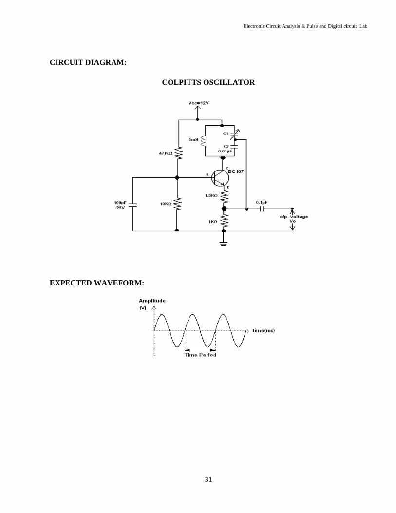
EXPERIMENT NO-4
(B) COLPITTS OSCILLATOR
AIM:
To find practical frequency of Colpitt’s oscillator and to compare it with theoretical
Frequency for L= 5mH and C= 0.001F, 0.0022F, 0.0033F respectively.
COMPONENTS & EQIUPMENT REQUIRED: -
S.No Device Range/
Rating
Quantity
(in No.s)
1 Colpitts Oscillator trainer board
containing
a) DC supply voltage
b) Inductors
c) Capacitor
d) Resistor
e) NPN Transistor
12V
5mH
0.01F
0.1F
100 F
0.001
0.0022
0.0033
1K
1.5K
10K
47K
BC 107
1
1
1
1
1
1
1
1
1
1
1
1
1
2 Cathode Ray Oscilloscope (0-20) MHz 1
3. BNC Connector 1
4 Connecting wires 5A 4
Electronic Circuit Analysis & Pulse and Digital circuit Lab
31
CIRCUIT DIAGRAM:
COLPITTS OSCILLATOR
EXPECTED WAVEFORM:

Electronic Circuit Analysis & Pulse and Digital circuit Lab
32
TABULAR COLUMN:
S.NO
L(mH) C1 (F) C2 (F) CT (F) Theoretical
Frequency
(KHz)
Practical
Frequency
(KHz)
Vo(V)
Peak to
peak
1 5 0.01 0.001
2 5 0.01 0.0022
3 5 0.01 0.0033
THEORY:
A Colpitts oscillator, invented in 1918 by American engineer Edwin H. Colpitts,[1] is one of a number
of designs for LC oscillators, electronic oscillators that use a combination of inductors (L) and
capacitors (C) to produce an oscillation at a certain frequency. The distinguishing feature of the Colpitts
oscillator is that the feedback for the active device is taken from a voltage divider made of two
capacitors in series across the inductor.The frequency of oscillation is approximately the resonant
frequency of the LC circuit, which is the series combination of the two capacitors in parallel with the
inductor
The actual frequency of oscillation will be slightly lower due to junction capacitances and resistive
loading of the transistor.As with any oscillator, the amplification of the active component should be
marginally larger than the attenuation of the capacitive voltage divider, to obtain stable operation. Thus,
a Colpitts oscillator used as a variable frequency oscillator (VFO) performs best when a variable
inductance is used for tuning, as opposed to tuning one of the two capacitors. If tuning by variable
capacitor is needed, it should be done via a third capacitor connected in parallel to the inductor (or in
series as in the Clapp oscillator).

Electronic Circuit Analysis & Pulse and Digital circuit Lab
33
PROCEDURE:
1. Connect the circuit as shown in the figure
2. Connect C2= 0.001F in the circuit and observe the waveform.
3. Calculate the time period and frequency of the waveform (f=1/T)
4. Now, fix the capacitance to 0.002 F and then to 0.003 F and calculate the
frequency and tabulate the reading as shown.
5. Find theoretical frequency from the formula
f = TLC2
1
Where 21
21
CC
CCCT
and compare theoretical and practical values.
6. Plot the graph o/p voltage vs time period and practical frequency
PRECAUTIONS:
1. No loose contacts at the junctions.
2. Check the connections before giving the power supply
3. Observations should be taken carefully.
RESULT:
Hence, the frequency of oscillations of Colpitts oscillator is measured practically and compared with
theoretical values .
1. For C=0.0022F & L= 5mH
Theoretical frequency = Practical frequency =
2. For C=0.0033F & L= 5mH
Theoretical frequency = Practical frequency =

Electronic Circuit Analysis & Pulse and Digital circuit Lab
34
3. For C=0.001F & L= 5mH
Theoretical frequency = Practical frequency =
VIVA QUESTIONS:
1. What are the applications of LC oscillations?
2. What type of feedback is used in oscillators?
3. What is the expression for the frequency of oscillations of Colpitt’s and Hartley oscillator?
4. Whether an oscillator is dc to ac converter. Explain?
5. What is the loop gain of an oscillator?
6. What is the difference between amplifier and oscillator?
7. What is the condition for sustained oscillations?
8. How many inductors and capacitors are used in Hartley Oscillator?
9. How the oscillations are produced in Hartley oscillator?
10. What is the difference between damped oscillations undamped oscillations?
11. How does Colpitt’s differ from Hartley?

Electronic Circuit Analysis & Pulse and Digital circuit Lab
35
EXPERIMENT NO 5
DARLINGTON EMITTER FOLLOWER
AIM: To study & plot the frequency response of a Darlington emitter follower circuit.
COMPONENTS & EQUIPMENT REQUIRED:
S.No Device Range/
Rating
Quantity
(in No.s)
1.
Trainer Board containing
a) DC Supply voltage.
b) NPN Transistor.
c) Resistors.
12 V
CL 100
4.7 KΩ
10 KΩ
1
2
1
1
2. Cathode Ray Oscilloscope. (0-20)MHz 1
3. Function Generator. 0.1 Hz-10
MHz
1
4 BNC Connector 2
5 Connecting Wires 5A 5

Electronic Circuit Analysis & Pulse and Digital circuit Lab
36
CIRCUIT DIAGRAM:
DARLINGTON EMITTER FOLLOWER
EXPECTED GRAPH:

Electronic Circuit Analysis & Pulse and Digital circuit Lab
37
TABULAR COLUMN :
Vin = 50 mV
Frequency
(in Hz)
Output
Voltage
(Vo)
Gain
(in dB) =
20log10(Vo/Vi)
20
40
80
100
500
1000
2000
5000
10K
50K
100K
200K
400K
600K

Electronic Circuit Analysis & Pulse and Digital circuit Lab
38
THEORY:
The Darlington transistor (often called a Darlington pair) is a compound structure consisting of two
bipolar transistors (either integrated or separated devices) connected in such a way that the current
amplified by the first transistor is amplified further by the second one. This configuration gives a much
higher common/emitter current gain than each transistor taken separately and, in the case of integrated
devices, can take less space than two individual transistors because they can use a shared collector.
Integrated Darlington pairs come packaged singly in transistor-like packages or as an array of devices
(usually eight) in an integrated circuit. A Darlington pair behaves like a single transistor with a high
current gain (approximately the product of the gains of the two transistors). In fact, integrated devices
have three leads (B, C and E), broadly equivalent to those of a standard transistor. A general relation
between the compound current gain and the individual gains is given by:
If β1 and β2 are high enough (hundreds), this relation can be approximated with:
Darlington pairs are available as integrated packages or can be made from two discrete transistors; Q1
(the left-hand transistor in the diagram) can be a low power type, but normally Q2 (on the right) will
need to be high power. The maximum collector current IC(max) of the pair is that of Q2. A typical
integrated power device is the 2N6282, which includes a switch-off resistor and has a current gain of
2400 at IC=10A.
A Darlington pair can be sensitive enough to respond to the current passed by skin contact even at safe
voltages. Thus it can form the input stage of a touch-sensitive switch.
800K
1000K
Electronic Circuit Analysis & Pulse and Digital circuit Lab
39
PROCEDURE:
a) Connect the circuit diagram as shown fig.
b) Adjust input signal amplitude in the function generator and observe an amplified voltage at the
output without distortion.
c) By keeping input signal voltage, say at 50 mV, vary the I/P signal frequency from 50Hz to 1 MHz
in step as shown in tabular column and note the corresponding O/P voltage.
d) Plot the graph between gain in (dB) vs frequency.
e) Calculate the maximum gain and bandwidth. BW=f2-f1
PRECAUTIONS:
1. No loose contacts at the junctions.
2. Check the connections before giving the power supply
3. Observations should be taken carefully.
RESULT:
Hence the frequency response Darlington emitter follower circuit has been studied and plotted
Gain: _____________________
Bandwidth: fH – fL = __________________
VIVA QUESTIONS:
1. What is the difference between emitter follower and Darlington pair ckt?
2. What is the value of i/p impedance of a typical Darlington pair ckt?
3. What is the value of o/p impedance of a typical Darlington pair ckt?
4. What is the value of current and voltage gain of a typical Darlington pair ckt?
5. Mention the applications of a Darlington pair ckt

Electronic Circuit Analysis & Pulse and Digital circuit Lab
40
EXPERIMENT NO: 6
MOS AMPLIFIER
AIM:
a) To Plot the frequency response of a common source amplifier.
b) Calculate gain.
c) Calculate bandwidth.
COMPONENTS & EQUIPMENTS REQUIRED:
S.No Device Range/Rating Quantity
(in No.s)
1. FET amplifier Trainer
Board with
(a) DC supply voltage
(b) FET
(c) Capacitors
(d) Resistors
12V
BFW 11
0.1F
47F
1.5K
4.7 K
1M
1
1
2
1
1
1
1
2. Signal generator 0.1Hz-1MHz 1

Electronic Circuit Analysis & Pulse and Digital circuit Lab
41
CIRCUIT DIAGRAM:
THEORY:
A common-source amplifier is one of three basic single-stage field-effect transistor (FET) amplifier
topologies, typically used as a voltage or transconductance amplifier. The easiest way to tell if a FET
is common source, common drain, or common gate is to examine where the signal enters and leaves.
The remaining terminal is what is known as "common". In this example, the signal enters the gate, and
exits the drain. The only terminal remaining is the source. This is a common-source FET circuit. The
analogous bipolar junction transistor circuit is the common-emitter amplifier. The common-source (CS)
amplifier may be viewed as a transconductance amplifier or as a voltage amplifier. As a
transconductance amplifier, the input voltage is seen as modulating the current going to the load. As a
voltage amplifier, input voltage modulates the amount of current flowing through the FET, changing
the voltage across the output resistance according to Ohm's law. However, the FET device's output
resistance typically is not high enough for a reasonable transconductance amplifier (ideally infinite),
nor low enough for a decent voltage amplifier (ideally zero). Another major drawback is the amplifier's
limited high-frequency response. Therefore, in practice the output often is routed through either a
voltage follower (common-drain or CD stage), or a current follower (common-gate or CG stage), to

Electronic Circuit Analysis & Pulse and Digital circuit Lab
42
obtain more favorable output and frequency characteristics. The bandwidth of the common-source
amplifier tends to be low, due to high capacitance resulting from the Miller effect. The gate-drain
capacitance is effectively multiplied by the factor .
TABULAR COLUMN :
Vin = 50 mV
Frequency
(in Hz)
Output
Voltage
(Vo)
Gain
(in dB) =
20log10(Vo/Vi)
20
40
80
100
500
1000
2000
5000
10K
50K
100K
200K
400K

Electronic Circuit Analysis & Pulse and Digital circuit Lab
43
PROCEDURE:
1. Connect the circuit diagram as shown in figure.
2. Adjust input signal amplitude in the function generator and observe an amplified voltage at the
output without 3.distortion.
3. By keeping input signal voltage, say at 50mV, vary the input signal frequency from 0 to 1MHz in
steps as shown in tabular column and note the corresponding output voltages.
4. Save the circuit and simulate.
5. Calculate the maximum gain and bandwidth using bode plotter. Compare the values with the
practical circuit values
PRECAUTIONS:
Check whether the connections are made properly or not.
RESULT:
Hence, the frequency response of FET (CS) amplifier is plotted
VIVA:
1. Draw the character sites of mosfet.
2. Define varies region of mosfet character sties.
3. Right the current equation for mosfet for varies region.
4. Define second order effect of a mosfet.
600K
800K
1000K

Electronic Circuit Analysis & Pulse and Digital circuit Lab
44
SIMULATION LAB
Electronic Circuit Analysis & Pulse and Digital circuit Lab
45
EXPERIMENT NO: 1
CE AMPLIFIER
AIM:
To plot the frequency response of CE amplifier and calculate gain bandwidth.
SOFTWARE REQUIRED: MultiSim Analog Devices Edition 10.0
COMPONENTS & EQUIPMENTS REQUIRED: -
S.No Apparatus Range/
Rating
Quantity
(in No.s)
1.
CE Amplifier trainer Board with
DC power supply
DC power supply
NPN transistor
Carbon film resistor
(e)Carbon film resistor
(f) Capacitor.
12V
5V
BC 107
100K, 1/2W
2.2K, 1/2W
0.1µF
1
1
1
1
1
2
2.
Cathode Ray Oscilloscope.
(0-20)MHz
1
3.
Function Generator. 0.1 Hz-10
MHz
1
4.
BNC Connector
2

Electronic Circuit Analysis & Pulse and Digital circuit Lab
46
5. Connecting Wires
5A
5
CIRCUIT DIAGRAM:
CE AMPLIFIER

Electronic Circuit Analysis & Pulse and Digital circuit Lab
47
EXPECTED GRAPH:
Bandwidth = fH-fL
TABULAR COLUMN:
Input voltage: Vi = 50mV
Frequency
(in Hz)
Gain (in dB) =
20 log 10 VO/ Vi
20
600
1K
2K
4K
8K
10K

Electronic Circuit Analysis & Pulse and Digital circuit Lab
48
20K
30K
40K
50K
60K
80K
100K
250K
500K
750K
1000K
THEORY:
The CE amplifier provides high gain & wide frequency response. The emitter lead is common to both
input and output circuits and is grounded. The emitter base is forward biased. The collector current is
controlled by the base current rather than emitter current. The input signal is applied to base terminal
of the transistor and amplifier output is taken across collector terminal. A very small change in base
current produces a much larger change in collector current. Frequency response of an amplifier is
defined as the variation of gain with respective frequency. The gain of the amplifier increases as the
frequency increases from zero till it becomes maximum at lower cut-off frequency and remains constant
till higher cut-off frequency and then it falls again as the frequency increases.
At low frequencies the reactance of coupling capacitor CC is quite high and hence very small part of
signal will pass through from one stage to the next stage.

Electronic Circuit Analysis & Pulse and Digital circuit Lab
49
At high frequencies the reactance of inter electrode capacitance is very small and behaves as a short
circuit. This increases the loading effect on next stage and service to reduce the voltage gain due to
these reasons the voltage gain drops at high frequencies.
At mid frequencies the effect of coupling capacitors is negligible and acts like short circuit, where as
inter electrode capacitors acts like open circuit. So, the circuit becomes resistive at mid frequencies and
the voltage gain remains constant during this range.
PROCEDURE:
1. Connect the circuit diagram as shown in figure.
2. Adjust input signal amplitude in the function generator and observe an amplified voltage at the
output without distortion.
3. By keeping input signal voltages at 50mV, vary the input signal frequency from 0 to 1MHz in
steps as shown in tabular column and note the corresponding output voltages.
4. Save the circuit and simulate.
5. Calculate the maximum gain and bandwidth using bode plotter. Compare the values with the
practical circuit values.
PRECAUTIONS:
Check whether the connections are made properly or not.
RESULT:
Frequency response of CE amplifier is plotted.
Gain, AV = ________dB.
Bandwidth= fH--fL =________Hz.
VIVA QUESTIONS:
1. What are the advantages and disadvantages of single-stage amplifiers?
2. Why gain falls at HF and LF?
3. Why the gain remains constant at MF?
4. Explain the function of emitter bypass capacitor, CE?
5. How the band width will effect as more number of stages are cascaded?
6. Define frequency response?
7. What is the phase difference between input and output waveforms of a CE amplifier?

Electronic Circuit Analysis & Pulse and Digital circuit Lab
50
EXPERIMENT NO: 2
COMMON SOURCE AMPLIFIER
AIM:
a) To Plot the frequency response of a common source amplifier.
b) Calculate gain.
c) Calculate bandwidth.
SOFTWARE REQUIRED: MultiSim Analog Devices Edition 10.0
COMPONENTS & EQUIPMENTS REQUIRED:
S.No Device Range/Rating Quantity
(in No.s)
1. FET amplifier Trainer
Board with
(a) DC supply voltage
(b) FET
(c) Capacitors
(d) Resistors
12V
BFW 11
0.1F
47F
1.5K
4.7 K
1M
1
1
2
1
1
1
1
2. Signal generator 0.1Hz-1MHz 1
THEORY:
The FET is a type of transistor commonly used for weak signal amplification. The
device can amplify analog or digital signals. It can also switch DC or function as an oscillator. In the
FET current flows along a semiconductor path called the channel. At one end of the channel, there is
an electrode called source. At the other end of the channel there is an electrode called the drain.

Electronic Circuit Analysis & Pulse and Digital circuit Lab
51
Frequency response of an amplifier is defined as the variation of gain with respective frequency. The
gain of the amplifier increases as the frequency increases from zero till it becomes maximum at lower
cut-off frequency and remains constant till higher cut-off frequency and then it falls again as the
frequency increases. At low frequencies the reactance of coupling capacitor CC is quite high and hence
very small part of signal will pass through from one stage to the next stage. At high frequencies the
reactance of inter electrode capacitance is very small and behaves as a short circuit. This increases the
loading effect on next stage and service to reduce the voltage gain due to these reasons the voltage gain
drops at high frequencies. At mid frequencies the effect of coupling capacitors is negligible and acts
like short circuit, where as inter electrode capacitors acts like open circuit. So, the circuit becomes
resistive at mid frequencies and the voltage gain remains constant during this range
CIRCUIT DIAGRAM:
COMMON SOURCE AMPLIFIER

Electronic Circuit Analysis & Pulse and Digital circuit Lab
52
EXPECTED GRAPH:
TABULAR COLUMN:
Input = 50mV
Frequency
(in Hz)
Gain
(in dB) =
20log10(Vo/Vi)
20
40
80
100
500
1000

Electronic Circuit Analysis & Pulse and Digital circuit Lab
53
5000
10K
50K
100K
200K
400K
600K
800K
PROCEDURE:
1. Connect the circuit diagram as shown in figure.
2. Adjust input signal amplitude in the function generator and observe an amplified voltage at the
output without 3.distortion.
3. By keeping input signal voltage, say at 50mV, vary the input signal frequency from 0 to 1MHz in
steps as shown in tabular column and note the corresponding output voltages.
4. Save the circuit and simulate.
5. Calculate the maximum gain and bandwidth using bode plotter. Compare the values with the
practical circuit values
PRECAUTIONS:
Check whether the connections are made properly or not.

Electronic Circuit Analysis & Pulse and Digital circuit Lab
54
RESULT:
Hence, the frequency response of FET (CS) amplifier is plotted.
Gain = _______dB (maximum).
3. Bandwidth= fH--fL = _________Hz.
VIVA QUESTIONS:
1. What is the difference between FET and BJT?
2. FET is unipolar or bipolar?
3. Draw the symbol of FET?
4. What are the applications of FET?
5. FET is voltage controlled or current controlled?
6. How does FET acts as an amplifier?
7. What are the advantages of FET over BJT?
8. What is the region of FET so that it acts as an amplifier?
9. What are the differences between JFET and MOSFET?

Electronic Circuit Analysis & Pulse and Digital circuit Lab
55
EXPERIMENT NO- 3
TWO STAGE RC COUPLED AMPLIFIER
AIM:
1. To plot the frequency response of a RC coupled amplifier with a pair of shunted emitter
capacitors of 10 μF and 100μF.
2. To calculate gain.
3. To calculate bandwidth.
SOFTWARE REQUIRED: MultiSim Analog Devices Edition 10.0
COMPONENTS & EQUIPMENT REQUIRED:
S.No Device Range/
Rating
Quantity
(in No.s)
1.
Trainer Board containing
a) DC Supply voltage.
b) NPN Transistor.
c) Resistors.
d) Capacitors.
12 V
BC 107
47 KΩ
2.2 KΩ
1 KΩ
10 KΩ
100F
10F.
1
2
2
2
5
2
6
2.
Bode Plotter
1
3.
Function Generator.
0.1 Hz-10
MHz
1

Electronic Circuit Analysis & Pulse and Digital circuit Lab
56
CIRCUIT DIAGRAM:
TWO STAGE RC COUPLED AMPLIFIER
EXPECTED GRAPH:

Electronic Circuit Analysis & Pulse and Digital circuit Lab
57
TABULAR FORM:
Vin = 50 mV
C=10μF C=100μF
S.No Frequency
(in Hz)
Gain(dB)
20
log(Vo/
Vi )
Frequency
(in Hz)
Gain(dB)
20
log(Vo/
Vi )
1 100
2 200
3 400
4 800
5 1K
6 2K
7 4K
8 8K
9 10K
10 20K
11 40K
12 80K
13 100K
14 200K

Electronic Circuit Analysis & Pulse and Digital circuit Lab
58
15 300K
16 500K
17 700K
18 900K
19 1M
THEORY:
As the gain provided by a single stage amplifier is usually not sufficient to drive the load, so to achieve
extra gain multi-stage amplifier are used. In multi-stage amplifiers output of one-stage is coupled to the
input of the next stage. The coupling of one stage to another is done with the help of some coupling
devices. If it is coupled by RC then the amplifier is called RC-coupled amplifier.
Frequency response of an amplifier is defined as the variation of gain with respective frequency. The
gain of the amplifier increases as the frequency increases from zero till it becomes maximum at lower
cut-off frequency and remains constant till higher cut-off frequency and then it falls again as the
frequency increases. At low frequencies the reactance of coupling capacitor CC is quite high and hence
very small part of signal will pass through from one stage to the next stage.
At high frequencies the reactance of inter electrode capacitance is very small and behaves as a short
circuit. This increases the loading effect on next stage and service to reduce the voltage gain due to
these reasons the voltage gain drops at high frequencies.
At mid frequencies the effect of coupling capacitors is negligible and acts like short circuit, where as
inter electrode capacitors acts like open circuit. So, the circuit becomes resistive at mid frequencies and
the voltage gain remains constant during this range.
Electronic Circuit Analysis & Pulse and Digital circuit Lab
59
PROCEDURE:
1. Connect the circuit as shown in figure for 10 μF.
2. Adjust input signal amplitude in the function generator and observe an amplified voltage at the
output without distortion.
3. By keeping input signal voltage, say at 50 mV, vary the input signal frequency from 0-1 MHz as
shown in tabular column and note the corresponding output voltage.
4. Save the circuit and simulate.
5. Calculate the maximum gain and bandwidth using Bode plotter. Compare the values with the
practical circuit values
6. Repeat the same procedure for C=100μF.
PRECAUTIONS:
Check whether the connections are made properly or not.
RESULT:
Hence, the frequency Response of RC coupled (2 stage) amplifier for 10μF and 100 μF is plotted.
1. For C=10 μF,
Gain= Bandwidth =fH – fL =
2. For C=100μF
Gain= Bandwidth =fH – fL =

Electronic Circuit Analysis & Pulse and Digital circuit Lab
60
VIVA:
1. What is the need for Cascading?
2. What are the types of Coupling Schemes for Cascading?
3. What are the advantages of RC coupling
4. What is the effect of bypass Capacitor on frequency response
5. What is the effect of Coupling Capacitors

Electronic Circuit Analysis & Pulse and Digital circuit Lab
61
EXPERIMENT NO-4
CURRENT SHUNT AND VOLTAGE SERIES FEEDBACK AMPLIFIER
AIM:
To study and plot the frequency response of a current shunt and voltage series feedback amplifier.
SOFTWARE REQUIRED: MultiSim Analog Devices Edition 13.0
COMPONENTS & EQUIPMENT REQUIRED:
S.No Apparatus Range/
Rating
Quantity
(in No.s)
1.
a) DC Supply voltage.
b) NPN Transistor.
c) Resistors.
d) Capacitor.
12 V
BC 107
47kΩ
2.2KΩ
10kΩ
1k
0.1 F.
22F.
1
2
2
2
1
2
1
3
3. Bode plotter 1
4. Function Generator. 0.1 Hz-10 MHz 1

Electronic Circuit Analysis & Pulse and Digital circuit Lab
62
CIRCUIT DIAGRAM:
Current shunt (with out capacitor)

Electronic Circuit Analysis & Pulse and Digital circuit Lab
63
Current shunt (with capacitor)
EXPECTED GRAPH:
THEORY:
Feedback plays a very important role in electronic circuits and the basic parameters, such as input
impedance, output impedance, current and voltage gain and bandwidth, may be altered considerably

Electronic Circuit Analysis & Pulse and Digital circuit Lab
64
by the use of feedback for a given amplifier. A portion of the output signal is taken from the output of
the amplifier and is combined with the normal input signal and thereby the feedback is accomplished.
There are two types of feedback. They are i) Positive feedback and ii) Negative feedback. Negative
feedback helps to increase the bandwidth, decrease gain, distortion, and noise, modify input and output
resistances as desired. A current shunt feedback amplifier circuit is illustrated in the figure. It is called
a series-derived, shunt-fed feedback. The shunt connection at the input reduces the input resistance and
the series connection at the output increases the output resistance. This is a true current amplifier.
TABULAR FORM:
Input voltage = 50mv
Voltage series
feedback
Current shunt
(without capacitor)
Current shunt(with
capacitor)
Frequency
Hz
Out
put
gain output gain Output Gain
20
40
60
100
200
400
600
800
1k
2k
5k
8k
10k
20k
40k
60k
100k

Electronic Circuit Analysis & Pulse and Digital circuit Lab
65
PROCEDURE:
1. Connect the circuit as shown in figure
2. Adjust input signal amplitude in the function generator and observe an amplified voltage at the
output without distortion.
3. By keeping input signal voltage, say at 50 mV, vary the input signal frequency from 0-1 MHz as
shown in tabular column and note the corresponding output voltage.
4. Save the circuit and simulate.
5. For current shunt feedback amplifier with shunt capacitor (with and without capacitor) voltage
series feedback amplifier (with and without feedback resistance). Repeat the above procedure.
6. Calculate the maximum gain and bandwidth using Bode plotter. Compare the values with the
practical circuit values
PRECAUTIONS:
1. No loose contacts at the junctions.
2. Check the connections before giving the power supply
3. Observations should be taken carefully.
RESULT:
Frequency responses for voltage series (with and without feedback amplifier),current
shunt (with and without capacitor are plotted)
400k
600k
800k
1M

Electronic Circuit Analysis & Pulse and Digital circuit Lab
66
EXPERIMENT NO-5
CASCODE AMPLIFIER
AIM:
1.To plot the frequency response of Cascode amplifier.
3. To calculate bandwidth.
SOFTWARE REQUIRED: MultiSim Analog Devices Edition 13.0
COMPONENTS & EQUIPMENT REQUIRED:
S.No Device Range/
Rating
Quantity
(in No.s)
1.
Trainer Board containing
a) DC Supply voltage.
b) NPN Transistor.
c) Resistors.
d) Capacitors.
12 V
2222
80 KΩ
4.7 KΩ
10nF
3
2
2
1
2
2
2.
Bode Plotter
1
3.
Function Generator.
0.1 Hz-10
MHz
1

Electronic Circuit Analysis & Pulse and Digital circuit Lab
67
CIRCUIT DIAGRAM:
EXPECTED WAVEFORM:

Electronic Circuit Analysis & Pulse and Digital circuit Lab
68
THEORY:
Cascode amplifier is a cascade connection of a common emitter and common base amplifiers. It is
used for amplifying the input signals. The common application of cascade amplifier is for impedance
matching. The low impedance of CE age is matched with the medium of the CB sage.
TABULAR COLUMN:
Input = 50mV
Frequency
(in Hz)
Gain
(in dB) =
20log10(Vo/Vi)
20
40
80
100
500
1000
5000
10K

Electronic Circuit Analysis & Pulse and Digital circuit Lab
69
50K
100K
200K
400K
600K
800K
PROCEDURE:
1. Connect the circuit as shown in figure
2. Adjust input signal amplitude in the function generator and observe an amplified voltage at the
output without distortion.
3. By keeping input signal voltage, say at 50 mV, vary the input signal frequency from 0-1 MHz as
shown in tabular column and note the corresponding output voltage.
4. Save the circuit and simulate.
5. Calculate the maximum gain and bandwidth using Bode plotter. Compare the values with the
practical circuit values
PRECAUTIONS:
Check whether the connections are made properly or not.
RESULT:
Hence, the frequency Response of cascode amplifier is plotted.

Electronic Circuit Analysis & Pulse and Digital circuit Lab
70
Gain=
Bandwidth =fH – fL =
VIVA QUESTIONS:
1. What is effect of coupling capacitor.
2. Draw the h parameter equivalent circuit for cascode amplifier
3. What short circuit current gain for cascode amplifier.
4. What are the characters ties of cascode
5. What are the application of cascade amplifier

Electronic Circuit Analysis & Pulse and Digital circuit Lab
71
EXPERIMENT NO-6
WEIN BRIDGE OSCILLATOR
AIM:
To find practical frequency of a wein bridge oscillator and to compare it with theoretical frequency
R1=10k R2= 8.2k and C1,C2 for 0.01uf ,0.022uf & 0.033uf.
SOFTWARE REQUIRED: MultiSim Analog Devices Edition 10.0
COMPONENTS AND EQUIPMENTS REQUIRED:
S.No Device Range/
Rating
Quantity
(in No.s)
1 wein bridge oscillator trainer
board containing
a) DC supply voltage
b) Capacitor
c) Resistor
d) NPN Transistor
e) Zener diode
12V-------
0.01F-------
4.7F------
0.022F------
0.033F----
1K-----------
10K---------
47K----------
8.2K---------
BC 107--------
5.1v
1
2
1
2
2
2
3
1
1
2
2
1
2 CRO 1

Electronic Circuit Analysis & Pulse and Digital circuit Lab
72
CIRCUIT DIAGRAM:
EXPECTED WAVEFORM
THEORY:
The Wien bridge oscillator employs a balanced wien bridge as the feedback network. Two stage CE
amplifier provides 360o phase shift to the signal. So the wien bridge need not introduce any phase
shift to satisfy Barkausen criterion .The attenuation of the bridges calculated to be 1/3 at resonant
frequency. So the amplifier stage should provide a gain of exactly 3 to make loop gain unity. Since
the gain of two stage amplifier is the product of individual stages , overall gain becomes very high.
But the gain will be trimmed down to 3 by negative feedback network. The emitter resistors of both
stages are kept unbypassed . This provides a current series feedback which ensures the stability of
operating point and reduction of gain. Frequency of oscillation is given by f = 1/2πRC

Electronic Circuit Analysis & Pulse and Digital circuit Lab
73
TABULATIONS:
S.No R1
kΩ
R2
kΩ
C1
µF
C2
µF
Theoretical
frequency
(KHz)
Practical
frequency (KHz)
Vo (V)
(ptp)
1 10 8.2 0.01 0.01
2 10 8.2 0.022 0.022
3 10 8.2 0.033 0.033
PROCEDURE:
1. Connect the circuit as shown in figure.
2. Connect C1& C2 to 0.01F capacitor in the circuit and observe the waveform.
3. Note the time period of the waveform and calculate the frequency: f = 1/T .
4. Now connect the capacitance to 0.022 F and 0.033F and calculate the frequency and
tabulate the readings as shown.
5. Find the theoretical frequency from the formula
6.
f =
R1=10k R2= 8.2k and C1,C2 for 0.01uf ,0.022uf & 0.033uf. Compare theoretical and
practical values.
PRECAUTIONS:
1. No loose contacts at the junctions.
2. Check the connections before giving the power supply
3. Observations should be taken carefully.

Electronic Circuit Analysis & Pulse and Digital circuit Lab
74
RESULT:
1. For C1 = 0.01F, & C2=0.01
Theoretical frequency = Practical frequency =
2. For C = 0.022F, &; C2=0.01
Theoretical frequency = Practical frequency =
3. For C = 0.033F, & 0.033µF
Theoretical frequency = Practical frequency =
VIVA QUESTIONS:
1. Give the formula for frequency of oscillations.
2. What is the total phase shift provided by the oscillator
3. What is the condition for wien bridge oscillator to generate oscillations
4. What is function of lead-lag network in wein bridge oscillator
5. Which type of feedback is used in wein bridge oscillator.
6. What gain of wein bridge oscillator.
7. What are the application of wein bridge oscillator.
8. What is the condition for oscillation.
9. What is the difference between damped oscillations undamped oscillations.
wein bridge oscillator is either LC or RC oscillator

Electronic Circuit Analysis & Pulse and Digital circuit Lab
75
EXPERIMENT NO-7
RC PHASE SHIFT OSCILLATOR
AIM:
To find practical frequency RC phase shift oscillator and to compare it with theoretical frequency for
R=10K and C = 0.01F, 0.0022F & 0.0033F respectively
SOFTWARE REQUIRED: MultiSim Analog Devices Edition 10.0
COMPONENTS AND EQUIPMENTS REQUIRED:
S.No Device Range/
Rating
Quantity
(in No.s)
1 RC phase shift oscillator trainer
board containing
a) DC supply voltage
b) Capacitor
c) Resistor
d) NPN Transistor
12V-----------
1000F-------
0.047F------
0.01F--------
0.0022F------
0.0033F----
1K-----------
10K---------
47K----------
100K---------
BC 107--------
1
1
1
3
3
3
1
4
1
1
1
2 CRO 1

Electronic Circuit Analysis & Pulse and Digital circuit Lab
76
CIRCUIT DIAGRAM:
RC PHASE SHIFT OSCILLATOR
EXPECTED WAVEFORM:
THEORY:
RC – phase shift oscillator has a CE amplifier followed by three sections of RC phase shift feedback
networks. The output of the last stage is return to the input of the amplifier.the values of R and C are
chosen such that the phase shift of each RC section is 600.thus,the RC ladder network produces a total
phase shift of 1800 between its input and output voltage for the given frequencies since CE amplifier
produces 1800 phase shift the total phase shift from the base of the transistor around the circuit and
back to the transistor will be exactly 3600 or 00.The frequency of oscillation is given by

Electronic Circuit Analysis & Pulse and Digital circuit Lab
77
F = 1/2ΠRC√6
PROCEDURE:
1. Connect the circuit as shown in figure.
2. Connect the 0.0022 F capacitors in the circuit and observe the waveform.
3. Save the circuit and simulate.
5. Calculate the time period and frequency of the resultant wave form. Compare the values with the
practical circuit values
6. Repeat the same procedure for C=0.033 F and 0.01F and calculate the frequency and tabulate as
shown.
5. Find theoretical frequency from the formula f = 1/2RC6 and compare theoretical and practical
frequencies.
PRECAUTIONS:
1. No loose contacts at the junctions.
2. Check the connections before giving the power supply
3. Observations should be taken carefully.
RESULT:
For C = 0.0022F & R=10K
Theoretical frequency= Practical frequency=
For C = 0.0033F & R=10K
Theoretical frequency= Practical frequency=
For C = 0.01F & R=10K
Theoretical frequency= Practical frequency=

Electronic Circuit Analysis & Pulse and Digital circuit Lab
78
TABULAR COLUMN:
S.No C
(F)
R
()
Theoretical
Frequency
(KHz)
Practical
Frequency
(KHz)
Vo (p-p)
(Volts)
1 0.0022 10K
2 0.0033 10K
3 0.01 10K

Electronic Circuit Analysis & Pulse and Digital circuit Lab
79
EXPERIMENT NO- 8
CLASS-A POWER AMPLIFIER (series fed)
AIM:
To study the frequency response of a series fed class-A power amplifier and calculate efficiency of
the amplifier circuit.
SOFTWARE REQUIRED: MultiSim Analog Devices Edition 10.0
COMPONENTS & EQUIPMENT REQUIRED:
S.No Apparatus Range/
Rating
Quantity
(in No.s)
1.
a) DC Supply voltage.
b) NPN Transistor.
c) Resistors.
d) Capacitor.
e) Inductor.
12 V
BC 107
560Ω
100KΩ
470Ω
22 F.
50mH
1
1
1
1
1
1
1
2. D.C Milliammeter 0-100mA 1
3. Bode plotter 1
4. Function Generator. 0.1 Hz-10 MHz 1

Electronic Circuit Analysis & Pulse and Digital circuit Lab
80
CIRCUIT DIAGRAM:
EXPECTED GRAPH:
THEORY:
Power amplifiers are mainly used to deliver more power to the load. To deliver more power it requires
large input signals, so generally power amplifiers are preceded by a series of voltage amplifiers. In
class-A power amplifiers, Q-point is located in the middle of DC-load line. So output current flows for
complete cycle of input signal. Under zero signal condition, maximum power dissipation occurs across
the transistor. As the input signal amplitude increases power dissipation reduces. The maximum
theoretical efficiency is 25%.

Electronic Circuit Analysis & Pulse and Digital circuit Lab
81
PROCEDURE:
1.Make the connections as per the circuit diagram.
2. Measure base, emitter and collector D.C voltages of both stages and compare against estimated
values.
3. Apply the input at input terminals of the circuit from the function generator.
4. Keep the input signal at constant frequency under mid frequency region and adjust the amplitude
such that output voltage undistorted.
5. Calculate the power efficiency and compare it with theoretical efficiency.
RESULT:
The maximum input signal amplitude which produces undistorted output signal is _________
The practical efficiency of the circuit is ________
VIVA QUESTIONS:
1. Differentiate between voltage amplifier and power amplifier
2. Why power amplifiers are considered as large signal amplifier?
3. When does maximum power dissipation happen in this circuit ?.
4. What is the maximum theoretical efficiency?
5. Sketch wave form of output current with respective input signal.
6. What are the different types of class-A power amplifiers available?
7. What is the theoretical efficiency of the transformer coupled class-A power amplifier?

Electronic Circuit Analysis & Pulse and Digital circuit Lab
82
8. What is difference in AC, DC load line?.
9. How do you locate the Q-point ?
10. What are the applications of class-A power amplifier?
TABULAR COLUMN:
S.No Frequency
(in Hz)
Gain(dB) Av =
20 log(Vo/ Vi )
1 100
2 200
3 400
4 800
5 1K
6 2K
7 4K
8 8K
9 10K
10 20K
11 40K
12 80K
13 100K
14 200K

Electronic Circuit Analysis & Pulse and Digital circuit Lab
83
CALCULATIONS:
Efficiency is defined as the ratio of AC output power to DC input power
DC input power = Vcc x ICQ
AC output power = VP-P2 / 8RL
Under zero signal condition:
Vcc = IBRB + VBE IBQ =( Vcc - VBE ) / RB
ICQ = β x IBQ VCE = Vcc - ICRC

Electronic Circuit Analysis & Pulse and Digital circuit Lab
84
EXPERIMENT - 9
CLASS B POWER AMPLIFIER (COMPLEMENTARY SYMMETRY
AIM: To study the CLASS B Complementary Symmetry amplifier and to calculate its
efficiency.
SOFTWARE REQUIRED: MultiSim Analog Devices Edition 10.0
COMPONENTS & EQUIPMENT REQUIRED:
S.No Apparatus Range/
Rating
Quantity
(in No.s)
1.
a) DC Supply voltage.
b) NPN Transistor.
c) Resistors.
d) Capacitor.
12 V
BC 107
220KΩ
1KΩ
1Ω
18KΩ
0.1 F.
1
2
1
1
1
2
2
2. D.C Milliammeter 0-100mA 1
3. Bode plotter 1
4. Function Generator. 0.1 Hz-10 MHz 1

Electronic Circuit Analysis & Pulse and Digital circuit Lab
85
CIRCUIT DIAGRAM:
EXPECTED GRAPH:
THEORY:
Power amplifiers are designed using different circuit configuration with the sole purpose of delivering
maximum undistorted output power to load. Push-pull amplifiers operating either in class-B are class-
AB are used in high power audio system with high efficiency. In complementary-symmetry class-B
power amplifier two types of transistors, NPN and PNP are used. These transistors acts as emitter
follower with both emitters connected together.
In class-B power amplifier Q-point is located either in cut-off region or in saturation region. So, that
only 180o of the input signal is flowing in the output. In complementary-symmetry power amplifier,
during the positive half cycle of input signal NPN transistor conducts and during the negative half cycle

Electronic Circuit Analysis & Pulse and Digital circuit Lab
86
PNP transistor conducts. Since, the two transistors are complement of each other and they are connected
symmetrically so, the name complementary symmetry has come
Theoretically efficiency of complementary symmetry power amplifier is 78.5%.
PROCEDURE:
1. Switch ON the CLASS B amplifier trainer.
2. Connect Milliammeter to (A) terminals and DRB to the RL terminals and fix RL=50Ω.
3. Apply the input voltage from the signal generator to the Vs terminals.
4. Connect channel 1 of CRO to the Vs terminals and channel 2 across the load.
5. By varying the input voltage, observe the maximum distortion less output waveform.
And note down the voltage reading.
6. Calculate the efficiency.
OBSERVATIONS: Vs=2v
FREQUENCY Vo
(volts)
Idc (mA) Efficiency
10 KHz
CALCULATIONS:
Pin=Vcc x Idc
Idc= L
o
R
V =
Pout =L
o
R
V
8
2
Efficiency= Po/Pi x100

Electronic Circuit Analysis & Pulse and Digital circuit Lab
87
RESULT: Thus efficiency of CLASS B (Complementary symmetry) amplifier calculated.
VIVA
1.Classfide large signal amplifier based of operating point.
2.state the advantages of push pull class b power amplifier over class b power amplifier .
3. what is harmonic distortion how even harmonic is eliminated using push pull
4. list advantages of complementary symmetry configuration over push pull amplifier.
5. What is covertion efficiency of class B power amplifier.

Electronic Circuit Analysis & Pulse and Digital circuit Lab
88

Electronic Circuit Analysis & Pulse and Digital circuit Lab
89
PULSE CIRCUITS

Electronic Circuit Analysis & Pulse and Digital circuit Lab
90
PULSE CIRCUITS LAB
INTRODUCTION:
Practical knowledge in electronic circuits and pulse circuits plays vital role in designing and developing
circuits for various applications. The PC lab was designed to give practical overview on different
amplifier circuits and pulse circuits. This Lab provides students with the opportunity to gain an
experience in connecting the circuits and studying the responses of these circuits. A software tool is
also provided for simulating the circuit.
This lab deals with the methods for the generation of pulse waveforms making use of semiconductor
devices like Diodes, Transistors and UJT’s. Pulse waveforms play a significant role in household
appliances like television radio and digital clocks. Their industrial applications include digital
instrumentation, Control Systems, digital Computers, data processing systems and CRO’s. The term
Pulse waveforms is popularly employed in electronics to refer to non-sinusoidal waveforms. These
waveforms play a vital role in electronic communication, and they are of immense help in pulse
Communication, television Engineering, radar, and telemetry.
Pulse waveforms change between the LOW and HIGH levels. A positive going pulse is one that goes from a normally
LOW logic level to a HIGH level and then back again. Digital waveforms are made up of a series of pulses.
Clock Signal Waveform
Active LOW - if the state change occurs from a “HIGH” to a “LOW” at the clock’s pulses falling
edge.
Duty Cycle - this is the ratio of the clock width to the clock period.
Clock Width - this is the time during which the value of the clock signal is equal to a logic “1”, or
HIGH.
Clock Period - this is the time between successive transitions in the same direction, ie, between two
rising or two falling edges.
Clock Frequency - the clock frequency is the reciprocal of the clock period, frequency = 1/clock
period
Electronic Circuit Analysis & Pulse and Digital circuit Lab
91
Most natural quantities that we see are analog and vary continuously. Analog systems can generally
handle higher power than digital systems Timing circuits networks composed of resistors, capacitors
and inductors are called linear network and they do not change the waveform of a sine wave when it is
transmitted through them. On the other hand when non-sinusoidal waveforms, (e.g. step, ramp,
exponential) are applied to the input of such networks the output signal may have very little resembles
with the input waveform. The action of a linear network in producing a waveform at its output different
from its input is called linear wave shaping. The wave shaping is used to perform any one of the
following functions.
1. To hold the waveform to a particular d.c. level.
2. To generate one wave form the other
3. To limit the voltage level of the waveform of some presenting value and suppressing all other
voltage levels in excess of the present level.
4. To cut-off the positive and negative portions of the input waveform.
Shaping circuits may be either series RC or series RL circuits. The series RC and RL circuits electrically
perform the mathematical operation of integration and differentiation. Therefore, the circuits used to
perform these operations are called integrators and differentiator. The differentiator circuits are used to
generate sharp narrow pulses either from distorted pulse waveform or from rectangular wave forms.
The integrator circuits are required to generate a voltage, which are required to generate a voltage,
which increases or decreases linearly with time.
The semiconductor Signal Diode is a small non-linear semiconductor devices generally used in
electronic circuits, where small currents or high frequencies are involved such as in radio, television
and digital logic circuits. The signal diode which is also sometimes known by its older name of the Point
Contact Diode or the Glass Passivated Diode, are physically very small in size compared to their
larger Power Diode cousins.
Electronic Circuit Analysis & Pulse and Digital circuit Lab
92
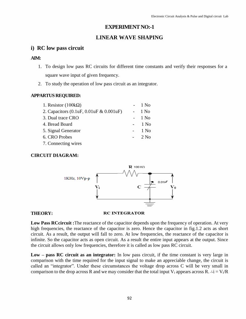
EXPERIMENT NO:-1
LINEAR WAVE SHAPING
i) RC low pass circuit
AIM:
1. To design low pass RC circuits for different time constants and verify their responses for a
square wave input of given frequency.
2. To study the operation of low pass circuit as an integrator.
APPARTUS REQUIRED:
1. Resistor (100kΩ) - 1 No
2. Capacitors (0.1uF, 0.01uF & 0.001uF) - 1 No
3. Dual trace CRO - 1 No
4. Bread Board - 1 No
5. Signal Generator - 1 No
6. CRO Probes - 2 No
7. Connecting wires
CIRCUIT DIAGRAM:
THEORY:
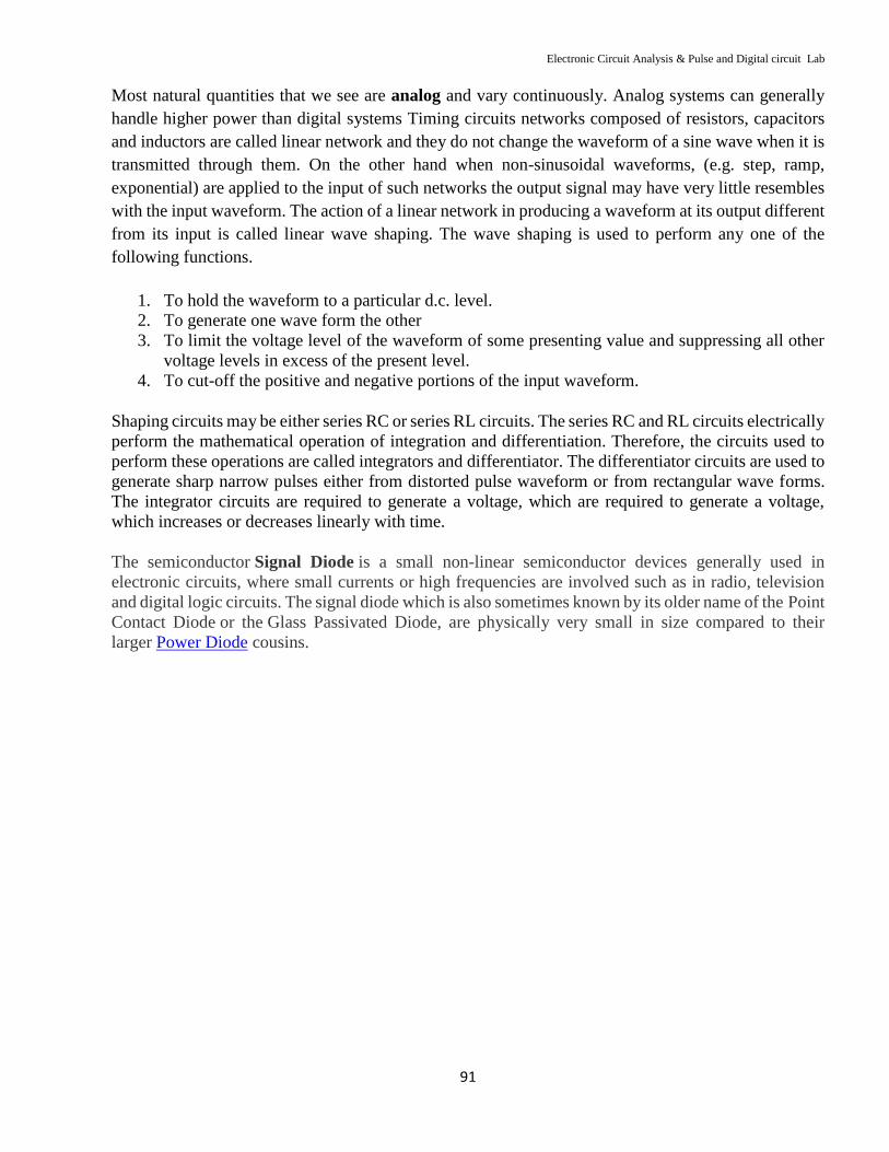
Low Pass RCcircuit :The reactance of the capacitor depends upon the frequency of operation. At very
high frequencies, the reactance of the capacitor is zero. Hence the capacitor in fig.1.2 acts as short
circuit. As a result, the output will fall to zero. At low frequencies, the reactance of the capacitor is
infinite. So the capacitor acts as open circuit. As a result the entire input appears at the output. Since
the circuit allows only low frequencies, therefore it is called as low pass RC circuit.
Low – pass RC circuit as an integrator: In low pass circuit, if the time constant is very large in
comparison with the time required for the input signal to make an appreciable change, the circuit is
called an “integrator”. Under these circumstances the voltage drop across C will be very small in
comparison to the drop across R and we may consider that the total input Vi appears across R. ∴i = Vi/R

Electronic Circuit Analysis & Pulse and Digital circuit Lab
93
DESIGN:
Choose T = 1msec ,For RC ˃˃ T ; the Low Pass Circuit as an Integrator
RC low pass circuit: (Design procedure for RC low pass circuit)
i) Long time constant: RC > > T ; Where RC is time constant and
T is time period of input signal.
Let RC = 10 T, Choose R = 100kΩ, f = 1kHz.
C = 10 / 103Χ 100Χ103 = 0.1µf
ii) Medium time constant: RC = T
C = T/R = 1/ 103Χ100Χ103 = 0.01µf
iii) Short time constant: RC < < T
RC = T/10 ⇒ C = T/10R = 1/ 10Χ103Χ100Χ103 = 0.001 µf.
a) RC=T
b) RC >>T
c) RC<< T

Electronic Circuit Analysis & Pulse and Digital circuit Lab
94
PROCEDURE:
1. Connect the circuit, as shown in figure.
2. Apply the Square wave input to the circuit (Vi = 10 VP-P, f = 1KHz)
3. Calculate the time constant of the circuit by connecting one of the Capacitor provided.
3. Observe the output wave forms for different input frequencies (RC<<T, RC=T, RC>˃T)
as shown in the tabular column for different time constants.
4. Plot the graphs for different input and output waveforms.
PRECAUTIONS:
1. Avoid loose and wrong connections.
2. Avoid eye contact errors while taking the observations in CRO.
OBSERVATIONS:
Low pass RC circuit:
S.No.
Time constant in
m. sec
O/P Voltage levels in Volts
1 RC=T
V1
V2
V1
2 RC>>T
V2
3 RC<<T V1

Electronic Circuit Analysis & Pulse and Digital circuit Lab
95
Low pass RC circuit:
Time constant in
m.sec
Output Signal Voltage
levels(Theoretical) in Volts Output Signal Voltage
levels(Practical) in Volts
Short time constant
(RC<<T)
Medium time
constant (RC=T)
Long time constant
(RC>>T)
REVIEW QUESTIONS:
1. Name the signals which are commonly used in pulse circuits and define any two of them?
2. Define linear wave shaping?
3. Define attenuator and types of attenuator?
4. Explain the fractional tilt of a high pass RC circuit. Write the Expression?
5. State the lower 3-db frequency of high-pass circuit?
6. Distinguish between the linear and non-linear wave shaping circuits.
7. Define Percentage Tilt and Rise time?
8. Show that a high pass circuit with a small time constant acts as differentiator?
9. Define Rise time? Give the relations between rise time and bandwidth?
10. Show that a low pass circuit with a time constant acts as Integrator?
11. Name a wave shaping circuit which produces a Ramp wave as an output by taking a step
signal as input and draw its output for a sinusoidal wave
12. Write the expressions for the output of a low pass circuit by a step and symmetrical square
waves?
13. Prove that for any periodic input wave form the average level of the steady state output signal
from an RC high pass circuit is always zero.
14. Explain the response of a high pass RC circuit to a step input signal?
15. Name a wave shaping circuit which produces a Ramp wave as an output by taking a step
signal as input and draw its output for a sinusoidal wave?
16. Write the expressions for the output of a low pass circuit by a step and symmetrical square
waves?

Electronic Circuit Analysis & Pulse and Digital circuit Lab
96
GRAPH:
RESULT: The characteristics of RC low pass circuit for different time constants are verified.
Electronic Circuit Analysis & Pulse and Digital circuit Lab
97
EXPERIMENT NO:-1
LINEAR WAVE SHAPING
ii) RC high pass circuit
AIM:
1. To design high pass RC circuits for different time constants and verify their responses
for a square wave input of given frequency.
2. To find the % tilt of high pass RC circuit for long time constant.
3. To study the operation of high pass RC circuit as a differentiator
APPARTUS REQUIRED:
1. Resistor (100kΩ) - 1 No
2. Capacitors (0.1uF, 0.01uF & 0.001uF) - 1 No
3. Dual trace CRO - 1 No
4. Bread Board - 1 No
5. Signal Generator - 1 No
6. CRO Probes - 2 No
7. Connecting wires
CIRCUIT DIAGRAM:
RC Differentiator
THEORY:
High Pass RC circuit :The reactance of the capacitor depends upon the frequency of operation. At
very high frequencies, the reactance of the capacitor is zero. Hence the capacitor in fig.1.1 acts as short
circuit. As a result the entire input appears at the output. At low frequencies, the reactance of the
capacitor is infinite. So the capacitor acts as open circuit. Hence no input reaches the output. Since the
circuit allows only high frequencies, therefore it is called as high pass RC circuit.

Electronic Circuit Analysis & Pulse and Digital circuit Lab
98
High – pass RC circuit as a differentiator:
In high pass RC circuit, if the time constant is very small in comparison with the time required for the
input signal to make an appreciable change, the circuit is called a “Differentiator”. Under these
circumstances the voltage drop across R will be very small in comparison with the drop across C. Hence
we may consider that the total input Vi appears across C. So that the current is determined entirely by
the capacitor. i = C dVi/dt.
The output signal voltage across R is Vo = RC dVi/dt. i.e. The output is proportional to the
differentiation of the input. Hence the high pass RC circuit acts as a differentiator for RC << T
DESIGN: RC high pass circuit:
i) Long time constant: RC > > T ; Where RC is time constant and
T is time period of input signal.
Let RC = 10 T, Choose R = 100kΩ, f = 1kHz.
C = 10 / 103Χ 100Χ103 = 0.1µf
iv) Medium time constant: RC = T
C = T/R = 1/ 103Χ100Χ103 = 0.01µf
v) Short time constant: RC < < T
RC = T/10 ⇒ C = T/10R = 1/ 10Χ103Χ100Χ103 = 0.001 µf.
EXPECTED WAVEFORMS:
a) RC=T
b) RC >>T

Electronic Circuit Analysis & Pulse and Digital circuit Lab
99
c) RC <<T
PROCEDURE:
1. Connect the circuit, as shown in figure.
2. Apply the Square wave input to the circuit (Vi = 10 VP-P, f = 1KHz)
3. Calculate the time constant of the circuit by connecting one of the Capacitor provided.
3. Observe the output wave forms for different input frequencies (RC<<T, RC=T, RC>˃T)
as shown in the tabular column for different time constants.
4. Plot the graphs for different input and output waveforms.
OBSERVATIONS:
S.No.
Time constant
in m.sec
O/P Voltage levels in Volts
1. RC=T
V1
V11
V2
V21
V1
V11
2
RC>>T
V2
V21
V1
3 RC<<T
V11
V2
V21

Electronic Circuit Analysis & Pulse and Digital circuit Lab
100
High Pass RC Circuit:
Time constant in
m.sec
Output Signal Voltage
levels(Theoretical) in Volts Output Signal Voltage
levels(Practical) in Volts
Short time constant
(RC<<T)
Medium time
constant (RC=T)
Long time constant
(RC>>T)
Time constant in
m.sec
%Tilt (Theoretical) %Tilt (Practical)
Short time constant
(RC<<T)
Medium time
constant (RC=T)
REVIEW QUESTIONS:
1. When HP-RC circuit is used as Differentiator?
2. Draw the responses of HPF to step, pulse, ramp inputs?
3. Draw the responses of LPF to step, pulse, ramp inputs?
4. Define % tilt and rise time?
5. When LP-RC circuit is used as integrator?
6. Why noise immunity is more in integrator than differentiator?
7. Why HPF blocks the DC signal?
8. What is meant by linear wave shaping?
9. Define time constant?

Electronic Circuit Analysis & Pulse and Digital circuit Lab
101
10. Differences between High pass and Low pass RC circuits?
11. What is the working principle of high pass and low pass RC circuits for non sinusoidal signal
inputs.
GRAPH:
RESULT: The characteristics of RC High pass circuit for different time constants are verified

Electronic Circuit Analysis & Pulse and Digital circuit Lab
102
EXPERIMENT NO:-2(a)
NON LINEAR WAVE SHAPING
CLIPPERS AIM:
To study the various clipper circuits and to plot the output waveforms for a sinusoidal input signal.
APPARATUS:
1. CRO (Dual Channel) - 1 No.
2. Signal Generator – 1 No.
3. Breadboard - 1 No.
4. Diode (1N4007) - 2 No.
5. Resistor (1 KΩ) - 1 No.
6. D.C Power Supply (dual) - 2 No.
7. Connecting wires
CIRCUIT DIAGRAMS& EXPECTED WAVEFORMS:

Electronic Circuit Analysis & Pulse and Digital circuit Lab
103
Negative Clipper

Electronic Circuit Analysis & Pulse and Digital circuit Lab
104
Negative Clipping wih positive reference voltage
TRANSFER CHARACTERISTIC CURVES:
Positive Clipper:
Positive Clipper with positive reference voltage

Electronic Circuit Analysis & Pulse and Digital circuit Lab
105
Positive Clipper with Negative reference voltage
Negative Clipper
Negative Clipper with positive reference voltage
Slicer:
PROCEDURE: -
1. Connect the circuit as shown in figure
2. Apply the input Sine wave to the circuit. (8Vp-p, 2 KHz)
3. Switch on the power supply and adjust the output of AF generator to 8V (peak to peak)

Electronic Circuit Analysis & Pulse and Digital circuit Lab
106
4. Observe the input and output waveforms on CRO and note down the readings.
5. Plot the graphs of input Vs output waveforms for different clipping circuits.
OBSERVATIONS:
PRECAUTIONS: -
1. Avoid loose and wrong connections.
2. Avoid parallax errors while taking the readings using CRO.
REVIEW QUESTIONS:
1. Define nonlinear wave shaping?
2. Define clipping circuit?
3. What is piecewise linear mode of a diode?
4. What are the different types of clippers?
5. Which kind of a clipper is called a slicer circuit?
6. What are the disadvantages of the shunt clipper?
7. Justify that a clamping circuit is a dc inserter?
8. Define Series clipper and shunt clipper?
9. Express the meaning of transmission region and attenuation region of a Clipping Circuit?
Sl
No.
Type of Clipper Reference
Voltage
Theoretical
Clipping
Voltage levels
Practical
Clipping
Voltage levels
1 Series Positive Clipper
0V
2V
-2V
2 Series Negative Clipper
0V
2V
-2V
3 Shunt Positive Clipper
0V
2V
-2V
4 Shunt Negative Clipper
0V
2V
-2V
5 Two level clipper

Electronic Circuit Analysis & Pulse and Digital circuit Lab
107
GRAPH:
RESULT: The characteristics of the different clippers using diodes are verified.

Electronic Circuit Analysis & Pulse and Digital circuit Lab
108
EXPERIMENT NO:-2(b)
NON LINEAR WAVE SHAPING
CLAMPERS AIM:
To study the various clamping circuits and to plot the output waveforms for a sinusoidal input
of given peak amplitude. (Choose f=1 kHz, Vp-p =8V)
APPARATUS:
1. CRO (Dual Channel) - 1 No.
2. Signal Generator - 1 No.
3. Breadboard - 1 No.
4. Diode (1N4007) - 1 No.
5. Resistor (100 KΩ) - 1 No.
6. Capacitor (1µF) - 1 No.
7. D.C Power Supply (dual) - 1 No.
8. Connecting wires
THEORY: The process whereby the form of a sinusoidal signals are going to be altered by transmitting
through a non-linear network is called non-linear wave shaping. Non-linear elements in combination
with resistors and capacitors can function as clamping circuit. A Clamping circuit is one that takes an
input waveform and provides an output i.e a faithful replica of its shape, but has one edge clamped to
the voltage reference point. The clamping circuit introduces the d.c component at the output side, for
this reason the clamping circuits are referred to as d.c restorer or d.c reinserted.
Clamping circuits are classified as two types.
i) Negative Clampers ii) Positive Clampers

Electronic Circuit Analysis & Pulse and Digital circuit Lab
109
CIRCUIT DIAGRAM:

Electronic Circuit Analysis & Pulse and Digital circuit Lab
110

Electronic Circuit Analysis & Pulse and Digital circuit Lab
111
PROCEDURE:-
1. Connect the circuit as shown in figures (1-5)
2. Switch on the power supply and adjust the output of AF generator to 8V (peak to peak)
3. Square wave input and Observe the output waveforms on CRO and note down the
Readings.
4. Plot the graphs of input Vs output waveforms for different clamping circuits.
OBSERVATIONS:
Sl No. Type of Clamper Reference
Voltage
Theoretical
Clamping
reference
Voltage level
Practical
Clamping
reference
Voltage level
1 Positive Clamper
0V
2V
-2V
2 Negative Clamper
0V
2V
-2V
PRECAUTIONS: -
1. Avoid loose and wrong connections.
2. Avoid parallax errors while taking the readings using CRO.
REVIEW QUESTIONS:
1. What are the applications of clamping circuits?
2. What is the synchronized clamping?
3. Why clamper is called as a dc inserter?
4. What is clamping circuit theorem. How the modified clamping circuit theorem does differs
from this?
5. Differentiate –ve clamping circuit from +ve clamping circuits in the above circuits?
6. Describe the charging and discharging of a capacitor in each circuit?

Electronic Circuit Analysis & Pulse and Digital circuit Lab
112
7. What is the function of capacitor?
GRAPH:
RESULT: The characteristics of the different clampers using diodes are verified

Electronic Circuit Analysis & Pulse and Digital circuit Lab
113
EXPERIMENT NO: 3
TRANSISTOR AS A SWITCH
AIM: To study and observe the switching characteristics of a transistor.
APPARTUS REQUIRED:-
1. Resistor – 2.2 KΩ, 68KΩ - 1 No
2. Transistor - BC 107 - 1 No
3. Dual trace CRO. - 1 No
4. Function generator. - 1 No
5. Probes - 2 No
6. Connecting wires.
CIRCUIT DIAGRAM:

Electronic Circuit Analysis & Pulse and Digital circuit Lab
114
EXPECTED WAVEFORM:
THEORY: The transistor Q can be used as a switch to connect and disconnect the load RL from the
source VCC. When a transistor is saturated, it is like a closed switch from the collector to the emitter.
When a transistor is cut-off, it is like an open switch
VCE = VCC
Saturation: The point at which the load line intersects the IB = 0 curve is known as cut-off. At this
point, base current is zero and collector current is negligible small i.e., only leakage current ICEO exists.
At cut-off, the emitter diode comes out of forward bias and normal transistor action is lost. The
transistor appears like a closed switch.
VCE(sat) ˜ VCC
The intersection of the load line and the IB = IB(sat) is called saturation. At this point base current is IB(sat)
and the collector current is maximum. At saturation, the collector diode comes out of reverse bias, and
normal transistor action is again lost.
PROCEDURE:-
1. Connect the circuit as shown in figure.
2. Switch on the power supply and observe the output of the function generator on CRO.
Adjust input signal amplitude such that output signal peak-to peak value is less than the
Saturation level.
3. Observe output waveforms on CRO and note down the readings.
4. Plot the graphs between input and output waveforms at a given input frequency.

Electronic Circuit Analysis & Pulse and Digital circuit Lab
115
Calculate the parameters: -
a) Rise Time (tr)
b) Fall Time (tf)
c) Delay Time (td)
d) Storage Time (ts)
e) Turn ON Time (tON)
f) Turn OFF Time (tOFF
Note:-
Rise Time: - It is the time taken to rise 10% of the Max value of the signal to 90% of
the Max value of the signal.
Fall Time: - It is the taken to fall 90% of the Max value of the signal to 10% of the
Max value of the signal.
Delay Time: - It is the time taken to rise from 0% to10% of the Max value of the signal.
Storage Time: - It is the time taken to fall from 100% to 90% of the Max value of the
Signal.
Turn ON Time: - It is the sum of Delay time and Rise time.
Turn OFF Time: - It is the sum of Storage time and fall time.
PRECAUTIONS: -
1. Avoid loose and wrong connections.
2. Aviod parallax error while taking the readings using CRO.
REVIEW QUESTIONS:
1. Name the devices that can be used as switches? 2. Draw the Practical and piece-wise linear diode V-I characteristics? 3. Describe the two regions of a diode? 4. Write the Expressions for the Static and dynamic resistance of a diode? 5. Define Forward recovery time and reverse recovery time? 6. Define Storage time and Transition time of a diode? 7. Explain how a Diode can be used as a switch? 8. Write short notes on Transistor switching times

Electronic Circuit Analysis & Pulse and Digital circuit Lab
116
GRAPH:
RESULT: -The switching characteristics of a transistor are verified.

Electronic Circuit Analysis & Pulse and Digital circuit Lab
117
EXPERIMENT NO: 4
BISTABLE MULTIVIBRATOR
AIM: To study the characteristics of bistable multivibrator using transistors.
APPARATUS REQUIRED:
1. CRO (Dual Channel) - 1 No.
2. Function Generator - 1 No.
3. CDS - 1 No.
5. Resistor (1 KΩ, 39 KΩ,3.9,10) - 2 No.
6 Capacitors (100 pF) - 2 No
7. Transistor (BC 107) - 2 No.
8. Diodes
9. Regulated D.C Power Supply (dual) - 1 No.
10. Connecting wires
CIRCUIT DIAGRAM:

Electronic Circuit Analysis & Pulse and Digital circuit Lab
118
EXPECTED WAVEFORMS:
THEORY:A Bistable circuit is one which can exist indefinitely in either of two stable states
and which can be induced to make an abrupt transition from one state to the other by means
of external excitation.
The Bistable circuit is also called as Bistable multivibrator, Eccles Jordon circuit, Trigger circuit, Scale-
of-2 toggle circuit, Flip-Flop & Binary. A Bistable Multivibrator is used in a many digital operations
such as counting and the storing of binary information. It is also used in the generation and processing
of pulse-type waveform. They can be used to control digital circuits and as frequency dividers. There
are two outputs available which are complements of one another. i.e. when one output is high the other
is low and vice versa .
Operation: When VCC is applied, one transistor will start conducting slightly more than that of the
other, because of some differences in the characteristics of a transistor. Let Q2 be ON and Q1 be OFF.
When Q2 is ON, The potential at the collector of Q2 decreases, which in turn will decrease the potential
at the base of Q1 due to potential divider action of R1 and R2. The potential at the collector of Q1
increases which inturn further increases the base to emitter voltage at the base of Q2. The voltage at the
collector of Q2 further decreases, which inturn further reduces the voltage at the base of Q1. This action
will continue till Q2 becomes fully saturated and Q1 becomes fully cutoff.
Thus the stable state of binary is such that one device remains in cut-off and other device remains at
saturation. It will be in that state until the triggering pulse is applied to it. It has two stable states. For
every transition of states triggering is required. At a time only one device will be conducting.
NEED OF COMMUTATING CAPACITORS (SPEED UP CAPACITORS): It is desired that the
transition should take place as soon as the trigger pulse is applied but such is not the case. When
transistor is in active region it stores charge in its base and when it is in the saturation region it stores

Electronic Circuit Analysis & Pulse and Digital circuit Lab
119
even none charge. Hence transistor cannot come out of saturation to cut-off. Until all such charges are
removed. The interval during which conduction transfer one transistor to other is called as the transition.
PROCEDURE:-
1. Connect the circuit as shown in Figure.
2. Observe the output of the square wave oscillator-using Oscilloscope.
3. Connect the output of square oscillator to the trigger input Of Bistable Circuit and observe output
waveforms using Oscilloscope.
4. By varying input signal (Trigger) frequency, observe both input and corresponding output Waveforms
Using Oscilloscope.
5. Plot the graph for input and output waveforms at different input (Trigger) frequencies.
OBSERVATIONS:
S.no Time period Voltage
1
2
PRECAUTIONS: -
1. Avoid loose and wrong connections.
2. Aviod parallax errors while taking the readings using CRO.
REVIEW QUESTIONS :
1. What are the applications of a Bitable Multivibrator?
2. Describe the operation of commutating capacitors?
3. Why is a Binary also called a flip-flop?
4. Mention the name of different kinds of triggering used in the circuit shown?
5. What are the disadvantages of direct coupled Binary?
6. How many types of unsymmetrical triggering are there?
7. What are catching diodes?

Electronic Circuit Analysis & Pulse and Digital circuit Lab
120
8. Which triggering is used in binary counting circuits?
GRAPH:
RESULT: The characteristics of Bistable Multivibrator using Transistors are verified.

Electronic Circuit Analysis & Pulse and Digital circuit Lab
121
EXPERIMENT NO:-5
ASTABLE MULTIVIBRATOR
AIM: To study the characteristics of Astable Multivibrator using transistors.
APPARATUS REQUIRED :
1. CRO (Dual Channel) - 1 No.
2. Function Generator – 1 No.
3. Breadboard - 1 No.
4. Resistor (2.2 KΩ, 47 KΩ) - 2 No. each
5. Capacitors (0.1µF) - 2 No.’s
6. 6. Transistor (BC 107) - 2 No.’s
7. Regulated D.C Power Supply (dual) - 1 No.
8. Connecting wires
.
CIRCUIT DIAGRAM:
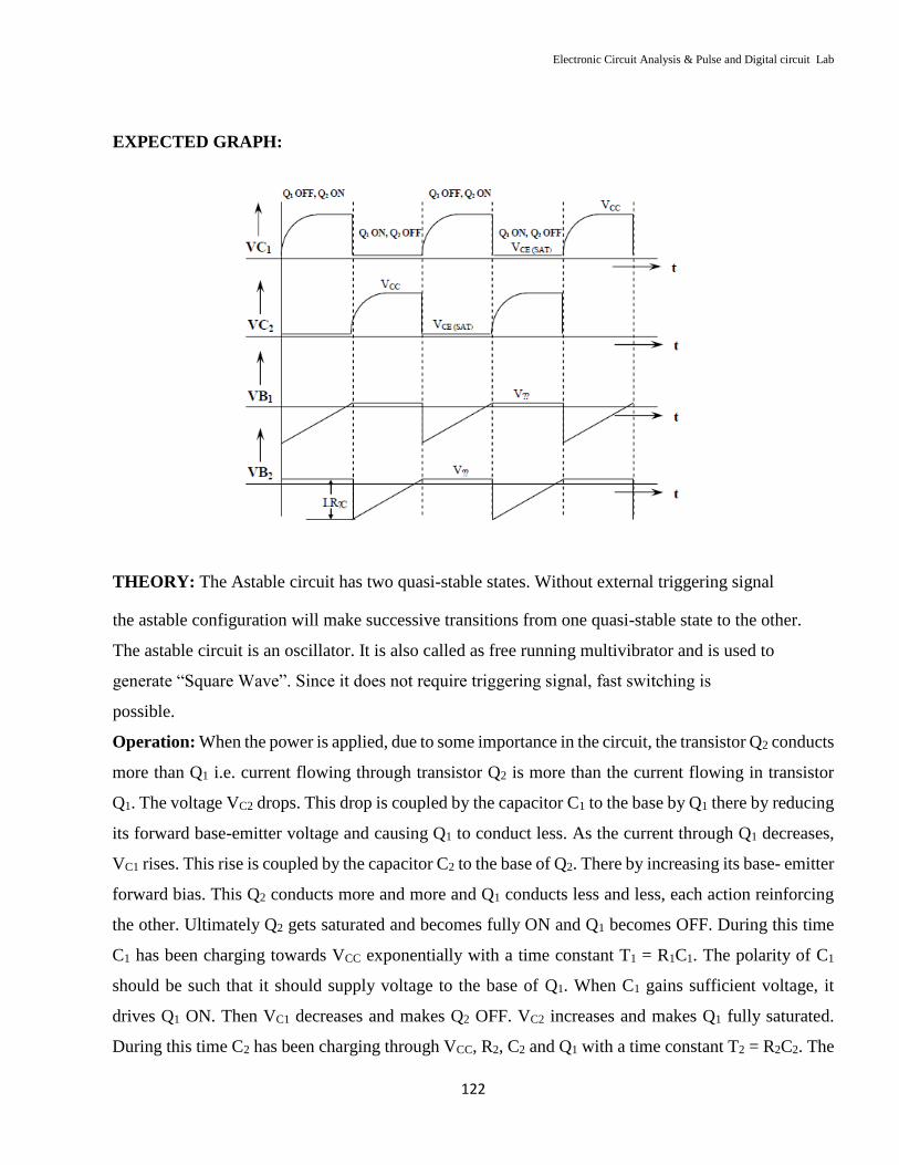
Electronic Circuit Analysis & Pulse and Digital circuit Lab
122
EXPECTED GRAPH:
THEORY: The Astable circuit has two quasi-stable states. Without external triggering signal
the astable configuration will make successive transitions from one quasi-stable state to the other.
The astable circuit is an oscillator. It is also called as free running multivibrator and is used to
generate “Square Wave”. Since it does not require triggering signal, fast switching is
possible.
Operation: When the power is applied, due to some importance in the circuit, the transistor Q2 conducts
more than Q1 i.e. current flowing through transistor Q2 is more than the current flowing in transistor
Q1. The voltage VC2 drops. This drop is coupled by the capacitor C1 to the base by Q1 there by reducing
its forward base-emitter voltage and causing Q1 to conduct less. As the current through Q1 decreases,
VC1 rises. This rise is coupled by the capacitor C2 to the base of Q2. There by increasing its base- emitter
forward bias. This Q2 conducts more and more and Q1 conducts less and less, each action reinforcing
the other. Ultimately Q2 gets saturated and becomes fully ON and Q1 becomes OFF. During this time
C1 has been charging towards VCC exponentially with a time constant T1 = R1C1. The polarity of C1
should be such that it should supply voltage to the base of Q1. When C1 gains sufficient voltage, it
drives Q1 ON. Then VC1 decreases and makes Q2 OFF. VC2 increases and makes Q1 fully saturated.
During this time C2 has been charging through VCC, R2, C2 and Q1 with a time constant T2 = R2C2. The

Electronic Circuit Analysis & Pulse and Digital circuit Lab
123
polarity of C2 should be such that it should supply voltage to the base of Q2. When C2 gains sufficient
voltage, it drives Q2 On, and the process repeats.
Design Procedure:
The period T is given by
T = T1 + T2 = 0.69 (R1C1 + R2C2)
For symmetrical circuit, with R1 = R2 = R & C1 = C2 = C
T = 1.38 RC
Let VCC = ; hfe = (for BC107), VBESat = ; VCESat = Let C = µF & T= .
T = 1.38 RC
R = KΩ
Choose ICmax = 10mA,
VCC −VCESAT
RC = =
IC max
TABLE:
S.NO OUTPUT VOLTAGES TRANSISTOR IN ON TRANSISTOR IS OFF
VC1
VC2
VB1
VB2
S.No Gate Width (Theoritical) Gate Width (Practical)

Electronic Circuit Analysis & Pulse and Digital circuit Lab
124
PROCEDURE:-
1. Connect The Circuit As Shown In Figure 1.
2. Observe The Output Of The Circuit Using Oscilloscope and measure the time Period Of The
Signal And Compare It With Theoretical Value By Varying Dc source V (5V to 10V) in steps
(take minimum two readings).
3. Plot the output waveforms on the graph paper for one set of values.
4. Repeat the steps from 1 to 3 with timing capacitor 0.01μF.
5. Connect the circuit as shown in figure 2.
6. Repeat the steps from 1 to 4.
PRECAUTIONS: -
1 Avoid loose and wrong connections.
2. Aviod parallax errors while taking the readings using CRO.
REVIEW QUESTIONS:
1. What are the other names of Astable Multivibrator?
2. Define quasi stable state?
3. Is it possible to change time period of the waveform with out changing R & C?
4. Collector waveforms are observed with rounded edges. Explain?
5. Explain charging and discharging of capacitors in an Astable Multivibrator?
6. How can an Astable Multivibrator be used as VCO?
7. Why do you get overshoots in the Base waveforms?
8. What are the applications of Astable Multivibrator?
9. How can Astable Multivibrator be used as a voltage to frequency converter?
10. What is the formula for frequency of oscillations?

Electronic Circuit Analysis & Pulse and Digital circuit Lab
125
GRAPH:
RESULT: -The characteristics of Astable multivibrator using transistors are verified.

Electronic Circuit Analysis & Pulse and Digital circuit Lab
126
EXPERIMENT NO:-6
MONOSTABLE MULTIVIBRATOR
AIM : To study the characteristics of Monostable Multivibrator using transistors.
APPARATUS REQUIRED:
1. CRO (Dual Channel) - 1 No.
2. Function Generator – 1 No.
3. CDS - 1 No.
4. Resistor (1 KΩ, 10 KΩ,100 KΩ,22 KΩ) - 1 No. each
5. Transistor (BC 107) - 2 No.
6. Regulated D.C Power Supply (dual) - 1 No.
7. Connecting wires
CIRCUIT DIAGRAM:-
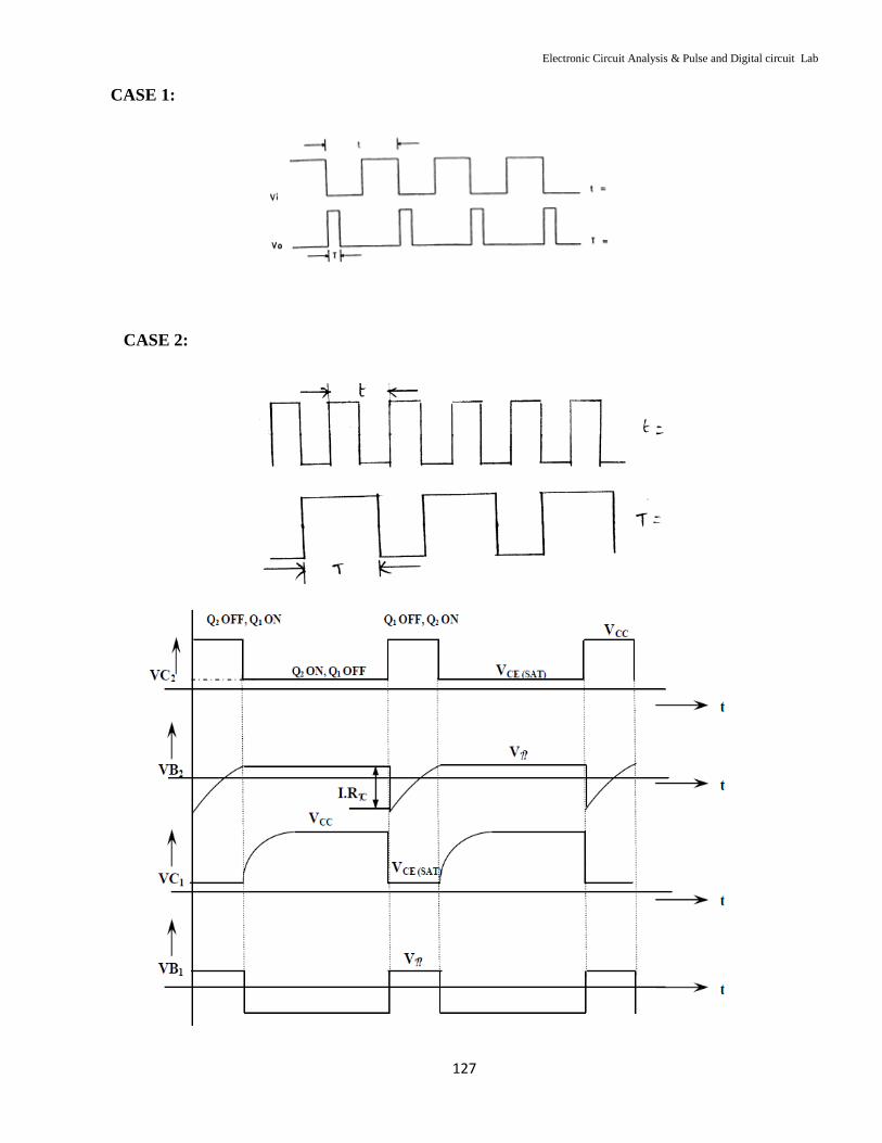
Electronic Circuit Analysis & Pulse and Digital circuit Lab
127
CASE 1:
CASE 2:

Electronic Circuit Analysis & Pulse and Digital circuit Lab
128
THEORY:-
The Monostable circuit has one permanently stable and one quasi-stable state. In the
monostable configuration, a triggering signal is required to induce a transition from the stable state to
the quasi-stable state. The circuit remains in its quasi-stable for a time equal to RC time constant of the
circuit. It returns from the quasi-stable state to its stable state without any external triggering pulse. It
is also called as one-shot a single cycle, a single step circuit or a univibrator.
Operation:
Assume initially transistor Q2 is in saturation as it gets base bias from VCC through R. coupling from
Q2 collector to Q1 base ensures that Q1 is in cutoff. If an appropriate negative trigger pulse applied at
collector of Q1 (VC1) induces a transition in Q2, then Q2 goes to cutoff. The output at Q2 goes high. This
high output when coupled to Q1 base, turns it ON. The Q1 collector voltage falls by IC1 RC1 and Q2 base
voltage falls by the same amount, as voltage across a capacitor ‘c’ cannot change instantaneously.
The moment, a –ve trigger is applied VC1, Q2 goes to cutoff and Q1 starts conducting. There is a path
for capacitor C to charge from VCC through R and the conducting transistor Q1. The polarity should be
such that Q2 base potential rises. The moment, it exceeds Q2 base cut-in voltage, it turns ON Q2 which
due to coupling through R1 from collector of Q2 to base of Q1, turns Q1 OFF. Now we are back to the
original state i.e. Q2 On and Q1 OFF. Whenever trigger the circuit into the other state, it cannot stay
there permanently and it returns back after a time period decided by R and C.
Pulse width is given as T = 0.69RCsec.
DESIGN:-

Electronic Circuit Analysis & Pulse and Digital circuit Lab
129
OBSERVATIONS:
S.NO OUTPUT VOLTAGES TRANSISTOR IN ON TRANSISTOR IS OFF
VC1
VC2
VB1
VB2
S.No Gate Width (Theoretical) Gate Width (Practical)
PROCEDURE:-
1. Connect the circuit as shown in figure.
2. Observe the output of the Square wave generator-using oscilloscope.
3. Connect the output of square oscillator to the trigger input of monostable circuit and also
Connect diode to the collector of the Q1.observe trigger spikes at Q1 collector using
Oscilloscope.
4. Connect one of the timing capacitor C to the circuit (say C=0.01μF) and observe the monostable at
collector of Q2 using oscilloscope.
5. Measure and note the pulse width of output signal and compare with the theoretical value (T=1.1RC).
6. By varying trigger input frequency, observe the corresponding output waveforms.
7. Plot the graph for input and output waveforms at different input frequencies.
8. Repeat the steps from 4 to 6 for timing capacitor C=0.1μF.
PRECAUTIONS: -
1. Avoid loose and wrong connections.
2. Avoid parallax while taking the readings using CRO.
REVIEW QUESTIONS:
1. What are applications of Monostable Multivibrator?
2. Why a Monostable Multivibrator is called a gating circuit?

Electronic Circuit Analysis & Pulse and Digital circuit Lab
130
3. Explain the waveform of VB1?
4. Describe the operation of the capacitor C3 in the circuit?
5. Why is the time period T also called Delay time?
6. Justify, Why Monostable Multivibrator is called one-shot circuit?
7. Why is the –ve voltage given at the base of Q1 transistor?
8. What is the no of quasi & stable states of Monostable Multivibrator?
9. What is meant by quasi stable state?
10. What is the function of commutating capacitors?
GRAPH:

Electronic Circuit Analysis & Pulse and Digital circuit Lab
131
RESULT: -The characteristics of Monostable multivibrator using transistors are verified

Electronic Circuit Analysis & Pulse and Digital circuit Lab
132
EXPERIMENT NO: 7
SCHMITT TRIGGER
AIM: To observe and note down the output waveforms of Schmitt trigger using transistors..
APPARATUS REQUIRED:
1. CRO (Dual Channel)
-
1 No.
2. Function Generator - 1 No.
3. CDS - 1 No.
4. Resistor (10 KΩ,150Ω) - 1 No each
5. Resistor (820Ω)
6. Resistor (1 KΩ)
-
-
2 No.’s
3 No.’s
7. Capacitors (0.022 µF,100 µF) - 1 No.
8. Transistor (BC107) - 2 No.
9. Regulated D.C. Power Supply (dual) - 1 No.
10. Connecting wires
CIRCUIT DIAGRAM:

Electronic Circuit Analysis & Pulse and Digital circuit Lab
133
EXPECTED WAVEFORMS:
THEORY:
In digital circuits fast waveforms are required i.e, the circuit remain in the active region for a very short
time (of the order of nano seconds) to eliminate the effects of noise or undesired parasitic oscillations
causing malfunctions of the circuit. Also if the rise time of the input waveform is long, it requires a
large coupling capacitor. Therefore circuits which can convert a slow changing waveform(long rise
time) in to a fast changing waveform (small rise time) are required. The circuit which performs this
operation is known as “Schmitt Trigger”.
In a Schmitt trigger circuit the output is in one of the two levels namely low or high. When the
output voltage is raising the levels of the output changes. When the output passes through a specified
voltage V1 known as Upper trigger level, similarly when a falling output voltage passes through a
voltage V2 known as lower triggering level. The level of the output changes V1 is always greater than
V2.The differences of these two voltages is known as “Hysteresis”.

Electronic Circuit Analysis & Pulse and Digital circuit Lab
134
TABLE:
S.NO OUTPUT VOLTAGES TRANSISTOR IN ON TRANSISTOR IS OFF
VC1
VC2
S.NO LTP UTP VH
PROCEDURE:
Observation of UTP and LTP:
1. Connect the circuit as per the circuit diagram.
2. Apply the square wave input of 1 KHz to the circuit.
3. Switch on the power supply and note down the amplitude and time period for the input square
wave.
4. Observe the output waveform and note down the amplitude and time period.
5. Keep Re1 and Re2 in minimum condition (extremely in anticlockwise direction)
6. Initially keep DC source voltage at zero and observe the output of the Schmitt trigger (it will be
in low state i.e. around 6V).
7. Vary the DC source output (i.e input voltage of the Schmitt trigger) slowly from zero.
8. Note down the input voltage value at which the output of the Schmitt trigger goes to high (UTP).
Still increase (upto 10V) the input voltage and observe that the output is constant.
9. Now slowly decrease the input voltage and note down the value at which the output of the
Schmitt trigger comes back to the original state (LTP).
10. Compare the values LTP and UTP with theoretical values.
Schmitt Trigger as a Squaring circuit:
1. Connect a triangle wave signal from an external function generator to the input of the level
changer.

Electronic Circuit Analysis & Pulse and Digital circuit Lab
135
2. Connect the output of the level changer to the input of the Schmitt trigger.
3. Connect CH1 input of CRO to the input signal and CH2 to the output of the schmitt trigger.
4. Adjust the amplitude of the input signal to such a level that we observe square wave at the
output.
5. Note down the points of input where the output is high (UTP) and low (LTP) and note that
both the levels are not one and the same.
6. Find Re1 value and compare it with the theoretical value.
7. Repeat the steps 3 to 6 with different types of signals (sine, ramp etc).
8. From the above observations we can notice that Schmitt trigger converts any arbitrary
waveform into a square/Rectangle wave.
CALCULATIONS:
Calculation of UTP:
1rEN VVUTP (Vr1 is cut in voltage i.e. 0.6 V)
)1(
)1()'( 2
feeb
feeBE
ENhRR
hRVVV (hfe of 2N 2369 is 50)
V’ and Rb is the Thevenins equivalent voltage and resistance between base of Q2 and ground when
Q1 is in cut-off.
= 211
112(
RRR
RRRR
c
cb
Calculation of LTP:
)'( 21 r
e
eBE VV
RaR
RVLTP
211
2'RRR
RVV
c
cc
Electronic Circuit Analysis & Pulse and Digital circuit Lab
136
21
2
RR
Ra
(a=Voltage ratio from collector of Q1 to base of Q2 )
211
112(
RRR
RRRR
c
c
(Where R is the Thevenins Equivalent Resistance when Q2 is
in cut-off)
PRECAUTIONS:
1. Avoid loose and wrong connections.
2. Avoid parallax errors while taking the readings using CRO.
REVIEW QUESTIONS:
1. What are the applications of Schmitt Trigger?
2. Define hysteresis action?
3. Why is Schmitt Trigger called a squaring circuit?
4. What is UTP & LTP?
6. What is the difference between a Binary and Schmitt Trigger?

Electronic Circuit Analysis & Pulse and Digital circuit Lab
137
GRAPH:
RESULT: The output waveforms of Schmitt trigger are observed.

Electronic Circuit Analysis & Pulse and Digital circuit Lab
138
EXPERIMENT NO: 9
UJT RELAXATION OSCILLATOR
AIM: To obtain a sawtooth waveform using UJT and test its performance as an oscillator.
APPARATUS REQUIRED:
1. CRO (Dual Channel)
-
1 No.
2. Function Generator - 1 No.
3. Bread Board - 1 No.
4. Resistor (47 KΩ,100Ω) - 1 No each
7. Capacitors (0.1µF) - 1 No.
8. Transistor (2N2646) - 1 No.
9. Regulated D.C. Power Supply (dual) - 1 No.
10. Connecting wires
CIRCUIT DIAGRAM :
1. Emitter . Base 2 1 3. Base2
Figure:5
V CC =12V R 1
C
B 2
B 1
E 47 KΩ
0.1 µ
?
F
R 2 100 Ω
?
2N2646

Electronic Circuit Analysis & Pulse and Digital circuit Lab
139
THEORY:
A Unijunction transistor (UJT), as the very implies, has only one p-n junction, unlike a BJT which has two p-n junctions’.
RB1 is the resistance between base B1 and the emitter, and it is basically a variable resistance, its value
being dependent upon the emitter current IE.
RB2 is the resistance between base B2 and the emitter, and the value is fixed.
Consider the circuit as shown in figure 1.
Let IE = 0. Due to the applied voltage VBB a current I.
Form the equivalent circuit, it is evident that the diode cannot conduct unless the emitter voltage VE =
V? + V1, where V? is the cutin voltage of the diode.
This value of the emitter voltage which makes the diode conduct is termed as peak voltage, and it is
denoted as VP.
We have VE = V? + V1,
It is obvious that if VE < VP, the UJT is OFF, and
if VE < VP, the UJT is ON.
Figure 3. shows the emitter characteristics of a UJT (plot of VE vs IE)
The equivalent circuit of the UJT is as shown in figure 1.
V BB
V 1 V E
I E
R B2
R B1
+
- Figure:1

Electronic Circuit Analysis & Pulse and Digital circuit Lab
140
The main application of UJT is in switching circuits wherein rapid discharging of capacitor is very
essential. Having understood the basic of UJT, we shall next study the working of UJT relaxation
oscillator.
Working of UJT relaxation oscillator (OR UJT sweep circuit)
V or VBB
+
The UJT sweep circuit shown in the figure 4 consists of a UJT, a capacitor and a resistor arranged as
shown.
We studied that a UJT is OFF as long as VE < VP, the peak voltage. Hence initially when the UJT is
OFF, the capacitor C charges through the resistance R from the supply voltage V.
Let VS = capacitor voltage.
It is seen that when the capacitor voltage VS rises to the value VP the UJT readily conducts. When the
UJT becomes ON, the capacitor discharges and its voltage falls. When the voltage falls to the valley
point VV, the UJT becomes OFF and the capacitor charges again to VP.
Figure 3.
0 I P I V I E
V V
V P
V E
Peak Point
Valley Point
Negative resistance
region
R B2
R B1
R
C V s
B 2
B 1
E
Figure:4

Electronic Circuit Analysis & Pulse and Digital circuit Lab
141
This cycle of charging and discharging of the capacitor C repeats, and as a result, a saw tooth
wave form of voltage across C is generated.
PROCEDURE:
1. Connect the circuit as shown in figure with designed values.
2. Note down the voltages and frequencies across C& R2 .
3. The time period of the output wave form is noted and is compared with theoretical value
T = R1 ? C[ ln (VBB – VV) / (VBB – VP)]
Plot the graphs of Vc and VR1.
REVIEW QUESTIONS:
1. Describe some important applications of a UJT?
2. Is the name UJT appropriate?
3. Write short notes on UJT as a relaxation oscillator?
4. Discuss the concept of –ve resistance?
5. Define the intrinsic stand off ratio and explain its importance?

Electronic Circuit Analysis & Pulse and Digital circuit Lab
142
GRAPH:
RESULT: Sawtooth waveform using UJT and test its performance as an oscillator is verified.

Electronic Circuit Analysis & Pulse and Digital circuit Lab
143
EXPERIMENT NO: 10
BOOTSTRAP SWEEP GENERATOR
AIM: To observe and note down the output waveforms of bootstrap sweep generator.
APPARATUS REQUIRED:
1. Resistors (10KΩ) – 4 No.
2. Resistors (1KΩ) - 1 No
3. Capacitor (1000µF) - 1 No
4. Capacitor (0.01µF) - 1 No
5. Diode (IN4148) - 1 No
6. Transistors ( 2N2222) - 2 No
7.. Dual CRO - 1 No.
8. Connecting wires.
CIRCUIT DIAGRAM:

Electronic Circuit Analysis & Pulse and Digital circuit Lab
144
THEORY: The input to Q1 is the gating waveform. Before the application of the gating waveform, at
t = 0, transistor Q1 is in saturation. The voltage across the capacitor C and at the base of Q2 is VCE(sat).
To ensure Q1 to be in saturation for t = 0, it is necessary that its current be at least equal to iCE / hFE so
that Rb < hfeR. With the application of the gating waveform at t = 0, Q1 is driven OFF. The current iC1
now flow into C and assuming units gain in the emitter follower V0 ? VCCt . When the sweep RC starts,
the diode is reverse biased, as already explained above, the current through R is supplied by C1. The
current VCC / R through C and R now flows from base to emitter of Q2.if the output V0 reaches the
voltage VCC in a time TS / Tg, then from above we have TS = RC.
EXPECTED WAVEFORMS:
F = 800Hz F = 3KHz
OBSERVATIONS:
S.No Frequency( Hz) Sweep time(TS) Restoration
time(TR)
Sweep
error(ES)
F = 800Hz
F = 3KHz
PROCEDURE:
1. Connect the circuit as per the circuit diagram.
2. Apply the square wave input of 1 KHz to the circuit.
3. Switch on the power supply and note down the amplitude and time period for the input square
wave.
4. Observe the output waveform and note down the amplitude and time period.

Electronic Circuit Analysis & Pulse and Digital circuit Lab
145
5. Plot the graphs for the input and output waveforms.
PRECAUTIONS:
1. Avoid loose and wrong connections.
2. Avoid parallax errors while taking the readings using CRO.
REVIEW QUESTIONS:
1. Define linear time base generator.
2. What is slope error in sweep generator?
3. What is transmission error in sweep generator?
4. Which amplifier is used to generate Miller sweep.
5. Which amplifier is used in miller time base generator?
6. Define the terms slope error, Transmission error and displacement error
7. Write the applications of time base generators?

Electronic Circuit Analysis & Pulse and Digital circuit Lab
146
GRAPH:
RESULT:- The output waveforms of Bootstrap sweep generator are observed.