Embed Size (px)
Citation preview
20 September 2007 "DSP Microprocessor Architectures" in IEP on VLSI-DSP Based Design, IIT Kharagpur 24-9-07 to 5-10-07
1
DSP Microprocessor Architectures
Indrajit Chakrabarti
Dept. of Electronics & E.C.E.
IIT Kharagpur
Email : [email protected]
20 September 2007 "DSP Microprocessor Architectures" in IEP on VLSI-DSP Based Design, IIT Kharagpur 24-9-07 to 5-10-07
2
DSP ProcessorA DSP processor is a microprocessor that
processes digitally represented signals
A filter takes discrete input xi[n] and and produces output y[n] for n=…,-1,0,1,…, and i=1,…,N where n is nth input or output at time n, and i is the ithcoefficient and N is length of the filter
DSP implements the discrete-time system
If signals are in continuous time domain, preprocessing is done using an ADC (analog-to-digital converter)
20 September 2007 "DSP Microprocessor Architectures" in IEP on VLSI-DSP Based Design, IIT Kharagpur 24-9-07 to 5-10-07
3
DSP Processor (contd.)DSP functions are operations on real-time signals;
these are repetitive and numerically intensive
Need of large memory bandwidth (as there can be millions of samples from real-time signals)
Architecture of a Digital Signal Processor is different than that of a conventional microprocessor
Most DSP operations are not complicated, involving only multiply and accumulate computations
Most DSP processors have hardwired circuitry to execute these calculations as fast as possible

20 September 2007 "DSP Microprocessor Architectures" in IEP on VLSI-DSP Based Design, IIT Kharagpur 24-9-07 to 5-10-07
4
A Finite-Impulse Response (FIR) Filter
An FIR filter performs a series of dot products. It takes an input vector and a vector of coefficients, performs point-wise multiplication between coefficients and a sliding window of input samples, and accumulates the multiplication results into an output sample
20 September 2007 "DSP Microprocessor Architectures" in IEP on VLSI-DSP Based Design, IIT Kharagpur 24-9-07 to 5-10-07
5
Handling MACsMultiply-Accumulate (MAC) operation is the most
often used operation in DSP
DSP processor has specialized hardware to perform single-cycle multiplication. An accumulator register (wider than other registers, providing guard bits to avoid overflow) is included in DSP architecture
DSP processor instruction set includes an explicit MAC instruction
MAC h/w and MAC instruction distinguishes early DSP processor and general-purpose processor (GPP)
20 September 2007 "DSP Microprocessor Architectures" in IEP on VLSI-DSP Based Design, IIT Kharagpur 24-9-07 to 5-10-07
6
Memory Architectures
von Neumann architecture
Harvard architecture

20 September 2007 "DSP Microprocessor Architectures" in IEP on VLSI-DSP Based Design, IIT Kharagpur 24-9-07 to 5-10-07
7
Memory Architectures (contd.)DSP algorithms require more memory bandwidth
than what is available in von Neumann architecture
Multiple memory accesses in one instruction cycle is required to sustain throughput of one FIR filter tap per instruction cycle
Two memory spaces (partitioned as program memory and data memory in Harvard architecture. The processor core is fed with data & instructions
In DSP processor, programmer controls which data & instructions are stored in on-chip memory banks
20 September 2007 "DSP Microprocessor Architectures" in IEP on VLSI-DSP Based Design, IIT Kharagpur 24-9-07 to 5-10-07
8
Zero-Overhead LoopingIn DSP algorithms, most of processing time is spent
to execute instructions contained in small loops
In FIR filter, inner loop multiplies input samples by their corresponding coefficients and add results
DSP processors include specialized hardware for zero-overhead looping
This h/w ensures that processor can execute loops without consuming cycles to test value of loop counter, do a conditional branch to top of the loop, and decrement the counter
20 September 2007 "DSP Microprocessor Architectures" in IEP on VLSI-DSP Based Design, IIT Kharagpur 24-9-07 to 5-10-07
9
Specialized AddressingParallel addressing mode specifies instructions
allowing concurrent use of functional units.
Modulo (circular) addressing is useful for implementing digital filter delay lines. Input is an infinite stream of data samples, which are windowed. Filter coefficients and data samples are stored in two circular buffers.
Bit-reversed addressing is useful for performing fast Fourier transform (FFT) using butterfly-based algorithms. Addresses of the outputs are bit-reversed with respect to the inputs.

20 September 2007 "DSP Microprocessor Architectures" in IEP on VLSI-DSP Based Design, IIT Kharagpur 24-9-07 to 5-10-07
10
DSP Instruction SetsDesign goals are
to enable processor to perform multiple operations per instruction cycle (to support this, a processor has multiple execution units capable of parallel operation)
to minimize amount of memory space required to store DSP programs (memory contributes significantly to overall system cost)
To keep processor fed with data without increasing program size, one can specify one or two parallel data moves (with address pointer updates) in parallel with some operations like MAC operations
20 September 2007 "DSP Microprocessor Architectures" in IEP on VLSI-DSP Based Design, IIT Kharagpur 24-9-07 to 5-10-07
11
Typical InstructionTake the following Motorola DSP56300 instruction (X and Y are two memory spaces of Harvard arch.)
MAC X0, Y0, A X: (R0)+,X0 Y: (R4)+N4,Y0
Tasks the processor performs are
• multiply contents of registers X0 and Y0
• add result to a running total kept in accumulator A
• load reg. X0 from X memory location pointed to by reg. R0
• load reg. Y0 from Y memory location pointed to by reg. R4
• post-increment R0 by 1 and R4 by contents of register N4
20 September 2007 "DSP Microprocessor Architectures" in IEP on VLSI-DSP Based Design, IIT Kharagpur 24-9-07 to 5-10-07
12
Case Study on DSP Processors1. Low-cost low-performance group : Analog
Devices’ ADSP-21xx, Texas Instruments’ TMS320C2xx, Motorola’s DSP560xx families. These operate at around 20 to 50 MIPs with modest power and memory use
2. Midrange (higher performance) DSP processors : Lucent Technologies’ DSP16xx and Texas Instruments’ TMS320C54x operate at 100 to 120 MIPs
20 September 2007 "DSP Microprocessor Architectures" in IEP on VLSI-DSP Based Design, IIT Kharagpur 24-9-07 to 5-10-07
13
ADSP-2181 DSP : Overview
• A programmable single-chip microcomputer with 20 ns instruction cycle time (40 MIPS sustained performance)
• Architecture has been designed for digital signal processing (DSP) and other high-speed numerical processing.
• Single-cycle instruction execution and context switch• 3-bus architecture helps fetch dual operands in an instruction
cycle• Multi-function instruction• Low power dissipation in Idle mode • Applications --- speaker phones, smart-card reader, video
conferencing, data encryption, ISDN modems, pattern matching, global positioning among others
20 September 2007 "DSP Microprocessor Architectures" in IEP on VLSI-DSP Based Design, IIT Kharagpur 24-9-07 to 5-10-07
14
Functional Units
• Three Computational units – an ALU, a MAC(multiplier-accumulator) and a Barrel Shifter
• Two data-address generators and a program sequencer
• Memory – a modified Harvard architecture in which data memory (DM) (of 16k word size) stores data, and program memory (PM) (of 16k word size) stores both instructions and data.

20 September 2007 "DSP Microprocessor Architectures" in IEP on VLSI-DSP Based Design, IIT Kharagpur 24-9-07 to 5-10-07
15
Functional Units (Contd)• Two serial ports provide serial interface with
hardware companding for data compression and expansion.
• A programmable interval timer with prescaler for periodic interrupt generation
• DMA ports --- Internal DMA Port (IDMA) and Byte DMA port (BDMA) for efficient data transfers to and from internal memory. and storing of program instructions and data.
20 September 2007 "DSP Microprocessor Architectures" in IEP on VLSI-DSP Based Design, IIT Kharagpur 24-9-07 to 5-10-07
16
Parallelism in ADSP-2181In a single cycle, the processor can• generate the next program address• fetch the next instruction• performs one or two data moves• update one or two data address pointers• performs a computation Also, in this same cycle, it can• receive and/or transmit data via the serial port(s)• receive and /or transmit data via the host interface port• receive and/or transmit data via the DMA ports
20 September 2007 "DSP Microprocessor Architectures" in IEP on VLSI-DSP Based Design, IIT Kharagpur 24-9-07 to 5-10-07
17
Features to Meet DSP Performance• Fast and Flexible Arithmetic --- single-cycle computation
for multiplication, multiplication with accumulation, arbitrary amounts of shifting, and standard arithmetic and logical tasks
• Extended Dynamic Range --- extended sums-of-products, common in DSP algorithms, are supported by multiply/accumulate units. A 40-bit accumulator gives 8 bits of protection against overflow in successive additions. Special instructions exist to implement block floating-point scaling of data
• Single-Cycle Fetch of Two Operands --- extended sums-of-products calculation is based on availability of two operands in each cycle. ADSP-2181 can sustain 2-operand data throughput, regardless of whether the data is stored on-chip or off-chip
20 September 2007 "DSP Microprocessor Architectures" in IEP on VLSI-DSP Based Design, IIT Kharagpur 24-9-07 to 5-10-07
18
Features to Meet DSP Performance (Contd)
• Hardware Circular Buffers --- implementation of DSP algorithms like digital filters requires the use of circular data buffers. The base architecture of ADSP-2100 family includes hardware to handle address pointer wraparound. This enables realization of circular buffers both on-chip and off-chip and reduces overhead, thus improving performance.
• Zero-Overhead Looping and Branching --- mostly repetitive DSP algorithms are logically expressed as loops. The program sequencer supports looped code with zero overhead. This enhances performance with simple program structure. Similarly, there are no overhead penalties for conditional branches
20 September 2007 "DSP Microprocessor Architectures" in IEP on VLSI-DSP Based Design, IIT Kharagpur 24-9-07 to 5-10-07
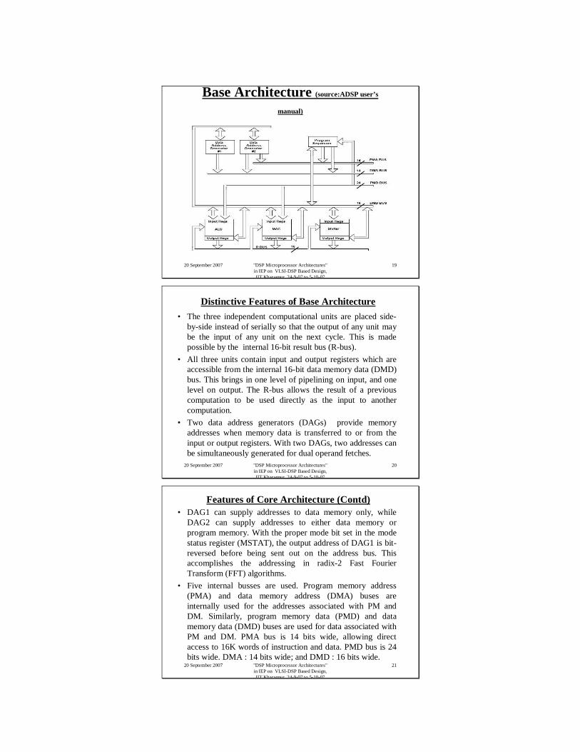
19
Base Architecture (source:ADSP user’s
manual)
20 September 2007 "DSP Microprocessor Architectures" in IEP on VLSI-DSP Based Design, IIT Kharagpur 24-9-07 to 5-10-07
20
Distinctive Features of Base Architecture• The three independent computational units are placed side-
by-side instead of serially so that the output of any unit may be the input of any unit on the next cycle. This is made possible by the internal 16-bit result bus (R-bus).
• All three units contain input and output registers which are accessible from the internal 16-bit data memory data (DMD) bus. This brings in one level of pipelining on input, and one level on output. The R-bus allows the result of a previous computation to be used directly as the input to another computation.
• Two data address generators (DAGs) provide memory addresses when memory data is transferred to or from the input or output registers. With two DAGs, two addresses can be simultaneously generated for dual operand fetches.
20 September 2007 "DSP Microprocessor Architectures" in IEP on VLSI-DSP Based Design, IIT Kharagpur 24-9-07 to 5-10-07
21
Features of Core Architecture (Contd)• DAG1 can supply addresses to data memory only, while
DAG2 can supply addresses to either data memory or program memory. With the proper mode bit set in the mode status register (MSTAT), the output address of DAG1 is bit-reversed before being sent out on the address bus. This accomplishes the addressing in radix-2 Fast Fourier Transform (FFT) algorithms.
• Five internal busses are used. Program memory address (PMA) and data memory address (DMA) buses are internally used for the addresses associated with PM and DM. Similarly, program memory data (PMD) and data memory data (DMD) buses are used for data associated with PM and DM. PMA bus is 14 bits wide, allowing direct access to 16K words of instruction and data. PMD bus is 24 bits wide. DMA : 14 bits wide; and DMD : 16 bits wide.
20 September 2007 "DSP Microprocessor Architectures" in IEP on VLSI-DSP Based Design, IIT Kharagpur 24-9-07 to 5-10-07
22
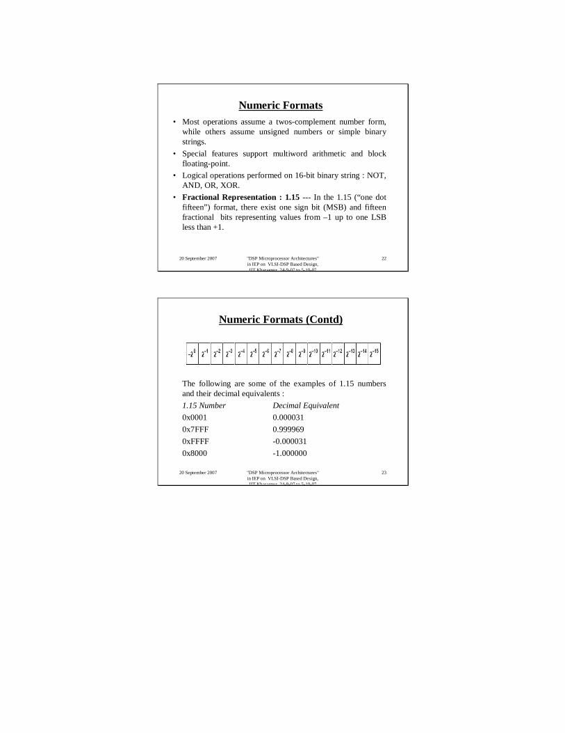
Numeric Formats• Most operations assume a twos-complement number form,
while others assume unsigned numbers or simple binary strings.
• Special features support multiword arithmetic and block floating-point.
• Logical operations performed on 16-bit binary string : NOT, AND, OR, XOR.
• Fractional Representation : 1.15 --- In the 1.15 (“one dot fifteen”) format, there exist one sign bit (MSB) and fifteen fractional bits representing values from –1 up to one LSB less than +1.
20 September 2007 "DSP Microprocessor Architectures" in IEP on VLSI-DSP Based Design, IIT Kharagpur 24-9-07 to 5-10-07
23
Numeric Formats (Contd)
The following are some of the examples of 1.15 numbers and their decimal equivalents : 1.15 Number Decimal Equivalent0x0001 0.0000310x7FFF 0.9999690xFFFF -0.0000310x8000 -1.000000

20 September 2007 "DSP Microprocessor Architectures" in IEP on VLSI-DSP Based Design, IIT Kharagpur 24-9-07 to 5-10-07
24
Arithmetic Logic Unit (ALU)• ALU provides a set of arithmetic and logic functions.
Arithmetic functions are : add, subtract, negate, increment, decrement, and absolute value. In addition, two division primitives exist with which multiple cycle division can be constructed. Logic functions are : AND, OR, OR (exclusive OR) and NOT.
• All operations on ALU treat operands and results as simple 16-bit binary strings. The two status bits, viz. overflow (AV) and negative (AN) treat the results as signed.
• Logic of overflow bit (AV) : it is set if MSB changes oddly; e.g. if adding two positive numbers changes sign bit, AV is set.
• Logic of carry bit (AC) : it is set if a carry is generated from bit 16 (MSB). The AC bit is useful for lower word portions of a multi-word operation.
20 September 2007 "DSP Microprocessor Architectures" in IEP on VLSI-DSP Based Design, IIT Kharagpur 24-9-07 to 5-10-07
25
Block Diagram of ALU (source:ADSP user’s manual)
20 September 2007 "DSP Microprocessor Architectures" in IEP on VLSI-DSP Based Design, IIT Kharagpur 24-9-07 to 5-10-07
26
Architecture of the ALU• ALU is 16 bits wide with two 16-bit input ports, X and Y,
and one output port, R. ALU accepts a carry-in signal CI, which is the carry bit from ASTAT (arithmetic status register).
• X input port of ALU can accept data from two sources : AX register file or the R-bus. AX register file ({AX0,AX1}) are readable and writeable from DMD bus. The register file outputs are dual-ported.
• Y input port can accept data from two sources : AY register file ({AY0,AY1}) and ALU feedback (AF) register. AY0 and AY1 are readable and writable from DMD bus and writeable from PMD bus. AY register file outputs are also dual-ported.
• Output of ALU is loaded into either ALU feedback (AF) register or ALU result (AR) register. AF register allows the ALU result to be directly used as Y input. AR can drive both DMD and R-bus.
20 September 2007 "DSP Microprocessor Architectures" in IEP on VLSI-DSP Based Design, IIT Kharagpur 24-9-07 to 5-10-07
27
Architecture of the ALU (Contd.)• Any ALU register can be both read and written in the same
cycle. Registers are read at the beginning of the cycle and written at the end of the cycle. This allows an input register to supply an operand to the ALU at the start of the cycle and be updated with the next operand from memory at the end of the same cycle.
• ALU has a duplicate bank of registers besides the primary bank of registers. That is, two sets of AR, AF, AX and AY register files exist. Only bank is accessible at a time. The additional bank is activated (e.g. during an interrupt service routine) for fast context switching. Thus a new task can be initiated without having to transfer the current states to storage.
• The bit 0 of processor mode status register (MSTAT) is made 0 to select the primary bank, and made 1 to select the alternate bank.
20 September 2007 "DSP Microprocessor Architectures" in IEP on VLSI-DSP Based Design, IIT Kharagpur 24-9-07 to 5-10-07
28
ALU Characteristics• Multi-precision operations --- supported in ALU with the carry-in
signal and ALU carry (AC) bit. The “add with carry” and “subtract with borrow” operations facilitate adding and subtracting, respectively, the upper portions of multi-precision numbers.
• ALU saturation mode --- AR register is set to maximum negative (viz. 0x8000) or positive value (0x7FFF) if an ALU result overflows orunderflows.
• ALU status --- bits of ASTAT register are as follows :– AZ (zero) : true if ALU output equals zero– AN (negative) : sign bit of ALU result; true if ALU output is
negative.– AV (overflow) : true if ALU overflows.– AC (carry) : carry output from most significant adder stage– AS (sign) : sign bit of ALU X input port; affected only by ABS
instruction– AQ (quotient) : quotient bit generated by division (DIVS and DIVQ)
instructions.
20 September 2007 "DSP Microprocessor Architectures" in IEP on VLSI-DSP Based Design, IIT Kharagpur 24-9-07 to 5-10-07
29
Multiplier/Accumulator Unit (MAC)• The MAC provides high-speed multiplication, multiplication with
cumulative addition, multiplication with cumulative subtraction,saturation and clear-to-zero functions.
• A feedback connection allows part of the accumulator output to be directly used as one of the multiplicands on the next cycle.
• Multiplier produces 32-bit result that is assumed to be signed, in that it is sign-extended across the full 40-bit width of MR register set. The nature of inputs is conveyed by the instruction itself (signed times signed, unsigned times unsigned, a mixture or rounding operation).
• Two modes of format adjustment are supported, viz. fractional mode for fractional operands, 1.15 format, and integer mode for integer operands, 16.0 format. When two 1.15 operands are multiplied, the result is a 2.30 number. In fractional mode, MAC shifts the multiplier product left one bit, causing the result to be in 1.31 format. In integer mode, there is no left shift. That is, two 16.0 operands, when multiplied, would produce a 32.0 result.
20 September 2007 "DSP Microprocessor Architectures" in IEP on VLSI-DSP Based Design, IIT Kharagpur 24-9-07 to 5-10-07
30
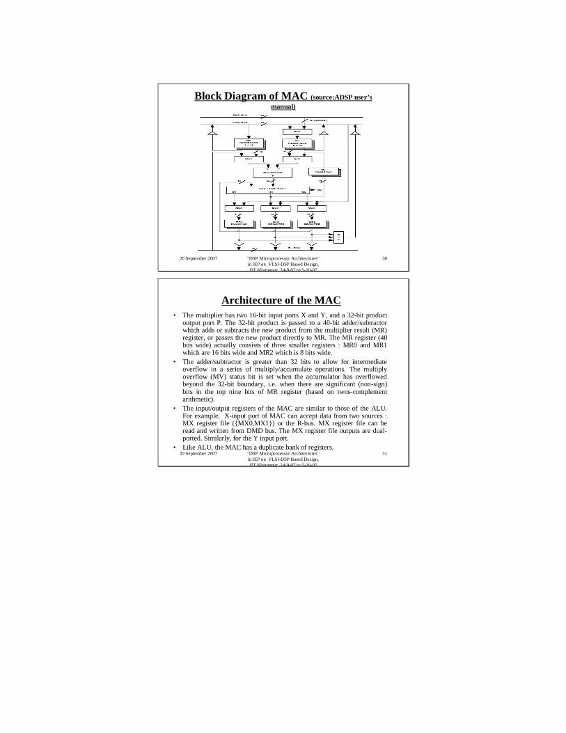
Block Diagram of MAC (source:ADSP user’s manual)
20 September 2007 "DSP Microprocessor Architectures" in IEP on VLSI-DSP Based Design, IIT Kharagpur 24-9-07 to 5-10-07
31
Architecture of the MAC• The multiplier has two 16-bit input ports X and Y, and a 32-bit product
output port P. The 32-bit product is passed to a 40-bit adder/subtractorwhich adds or subtracts the new product from the multiplier result (MR) register, or passes the new product directly to MR. The MR register (40 bits wide) actually consists of three smaller registers : MR0 and MR1 which are 16 bits wide and MR2 which is 8 bits wide.
• The adder/subtractor is greater than 32 bits to allow for intermediate overflow in a series of multiply/accumulate operations. The multiply overflow (MV) status bit is set when the accumulator has overflowed beyond the 32-bit boundary, i.e. when there are significant (non-sign) bits in the top nine bits of MR register (based on twos-complement arithmetic).
• The input/output registers of the MAC are similar to those of the ALU. For example, X-input port of MAC can accept data from two sources : MX register file ({MX0,MX1}) or the R-bus. MX register file can be read and written from DMD bus. The MX register file outputs are dual-ported. Similarly, for the Y input port.
• Like ALU, the MAC has a duplicate bank of registers.
20 September 2007 "DSP Microprocessor Architectures" in IEP on VLSI-DSP Based Design, IIT Kharagpur 24-9-07 to 5-10-07
32
MAC Operations• Standard functions --- are
– X*Y multiply X and Y operands– MR + X*Y multiply X and Y operands and add result to MR register– MR - X*Y multiply X and Y operands and subtract result from MR register– 0 clear result (MR) to zero
• MAC Overflow and Saturation --- adder/subtracter generates a true overflow status signal (MV) (which is loaded into ASTAT register) when the accumulator result crosses the 32-bit (MR1/MR2) boundary (that is, when the upper nine bits of MR are not all ones or all zeros). The saturation capability of MR sets it to the maximum positive or negative value if an overflow (indicated by MV=1 and MSB of MR2=1) or an underflow (indicated by MV=1 and MSB of MR2=0) occurs.
• Rounding mode --- the accumulator has the capability to round the 40-bit result R at the boundary between bit 15 and bit 16. Rounding is specified as part of the instruction code. The rounded output is directed to either MR or MF.
20 September 2007 "DSP Microprocessor Architectures" in IEP on VLSI-DSP Based Design, IIT Kharagpur 24-9-07 to 5-10-07
33
Barrel Shifter• The barrel shifter provides a complete set of shifting
functions for a 16-bit input, yielding a 32-bit output. These include arithmetic shift, logical shift and normalization. The shifter also performs derivation of exponent, and derivation of common exponent for an entire block of numbers. The basic functions can be combined to efficiently implement any degree of numerical format control, including full floating-point representation.
• Many operations in the shifter are specifically meant for signed (twos-complement) or unsigned values : logical shifts assume unsigned-magnitude or binary string values and arithmetic shifts assume twos-complement.
• The exponent logic assumes twos-complement numbers. The exponent logic supports block floating-point, which is based on twos-complement fractions.

20 September 2007 "DSP Microprocessor Architectures" in IEP on VLSI-DSP Based Design, IIT Kharagpur 24-9-07 to 5-10-07
34
Barrel Shifter (source:ADSP user’s manual)
20 September 2007 "DSP Microprocessor Architectures" in IEP on VLSI-DSP Based Design, IIT Kharagpur 24-9-07 to 5-10-07
35
Architecture of the Shifter• The shifter can be divided into the following components, viz. the shifter
array, the OR/PASS logic, the exponent detector and the exponentcompare logic.
• The shifter array is a 16X32 barrel shifter. It accepts a 16-bit input and can place it anywhere in the 32-bit output field, from off-scale right to off-scale left, in a single cycle. This gives 49 possible placements within the 32-bit field. The positioning of the 16 input bits is determined by a control code (C) and a HI/LO reference signal.
• Shifter array and associated logic are surrounded by a set of registers. The shifter input (SI) register provide input to shifter array and exponent detector. SI is 16 bits wide and is readable and writable from DMD bus. The input to shifter array and exponent detector can also come from AR, SR or MR via R-bus. The shifter result (SR) register is 32 bits wide, and is divided into two 16-bit sections, SR0 and SR1. The SR0 and SR1 registers can be loaded from DMD bus and output to either DMD or R-bus. The SR register is also fed back to the OR/PASS logic to allow double-precision shift operations.
• The shifter exponent (SE) register is 8 bits wide and holds the exponent during the normalize and denormalize operations. It is a 2’s-complement, 8.0 value.
20 September 2007 "DSP Microprocessor Architectures" in IEP on VLSI-DSP Based Design, IIT Kharagpur 24-9-07 to 5-10-07
36
Architecture of the Shifter (Contd)• The shifter block (SB) register is important in block floating-point
operations where it holds the block exponent value, that is, the value by which the block values must be shifted to normalize the largest value. SB is 5 bits wide and holds the most recent block exponent value. The SB register, which is loadable and readable from the lower 5 bits of the DMD bus, is a twos-complement, 5.0 value. Whenever the SE or SB registers are output onto the DMD bus, they are sign-extended to form a 16-bit value.
• The shifting of the input is determined by a control code (C) and a HI/LO reference signal. The control code is an 8-bit signed value which indicates the direction and number of places by which the input is to be shifted. Positive codes and negative codes indicate left (up) shift and right (down) shift respectively. The HI/LO signal determines thereference point for shifting. In the HI state, all shifts are referenced to SR1 (upper half of output field), and in the LO state, all shifts are referenced to SR0 (lower half).
• The shifter fills any bits to the right of the input value in the output filed with zeros, and bits to the left are filled with the extension bit (X). Depending on the instruction performed, extension bit can be MSB of input, AC bit o a zero.
20 September 2007 "DSP Microprocessor Architectures" in IEP on VLSI-DSP Based Design, IIT Kharagpur 24-9-07 to 5-10-07
37
Architecture of the Shifter (Contd)• The OR/PASS logic allows the shifted sections of a multi-precision
number to be combined into a single quantity. In some shifter instructions, the shifted output may be logically OR-ed with the contents of the SR register. When the [SR OR] option is not used in the instruction, the shifter array output is passed through and loaded into the shifter result (SR) register unmodified.
• The exponent detector derives an exponent for the shifter input value. In the HI state, input is interpreted as a single precision number. The detector determines the number of leading sign bits and produces a code to indicate how many places the input must be shifted to remove all but one sign bit.
• The exponent compare logic is used to find the largest exponent value in an array of shifter input values. The exponent compare logic with the help of the exponent detector derives a block exponent. The comparator compares the exponent value derived by the detector with the value stored in shifter block (SB) register and updates the SB register only when the derived exponent value is larger than the value in the SB register.
20 September 2007 "DSP Microprocessor Architectures" in IEP on VLSI-DSP Based Design, IIT Kharagpur 24-9-07 to 5-10-07
38
Shifter Operations• The shifter performs the following functions (mnemonics in parenthesis)
: Arithmetic Shift (ASHIFT), Logical Shift (LSHIFT), Normalize (NORM), Derive Exponent (EXP), Block Exponent Adjust (EXPADJ)
• The above basic shifter instructions can perform following functions for single precision or double precision – Derivation of a Block Exponent – Immediate Shifts– Denormalization– Normalization
• The shift functions (arithmetic and logical shift and normalize) can be specified with [SR OR] and HI/LO modes to perform multi-precision operations
• Derive Block Exponent --- detects the exponent of the largest number in an array using the EXPADJ instruction. Following is the step sequence :-
load SB with –16 (SB: used to contain exponent for the entire block)process first element : Array[(1)= 11110101 10110001; Exponent=-3; SB gets –3process next array element : Array(2)=00000001 01110110; Exp=-6; SB remains –3continue processing the remaining array elements
20 September 2007 "DSP Microprocessor Architectures" in IEP on VLSI-DSP Based Design, IIT Kharagpur 24-9-07 to 5-10-07
39
Shifter Operations (Contd)• Immediate Shifts --- shifts the input bit pattern to the right (downshift)
or left (upshift) by a given number of bits. Following example shows input value downshifted relative to upper half of SR (SR1).
SI = 0xB6A3;
SR = LSHIFT SI BY –5 (HI);Input : 10110110 10100011; Shift value : -5SR : 00000101 10110101 00011000 00000000
• Normalize --- process of shifting a twos-complement number in a field so that the rightmost sign bit lies up with the MSB position of field, and recording how many places the number was shifted. It is a two-stage process. First stage derives exponent (using EXP instruction). Second stage does actual shifting (using NORM instruction). Following is an example for single precision.
SE = EXP AR (HI);Input : 11110110 11010100; SE set to : -3 (as there are 3 redundant sign bits)Normalize now, with modifier = HI, shift being dictated by value in SESR : 10110110 10100000 00000000 00000000
20 September 2007 "DSP Microprocessor Architectures" in IEP on VLSI-DSP Based Design, IIT Kharagpur 24-9-07 to 5-10-07
40
Program Control• Program Sequencer --- controls the flow of program
execution. It contains an interrupt controller and status and condition logic. It generates a stream of instruction addresses. It allows sequential instruction execution, zero-overhead looping, sophisticated interrupt servicing, and single-cycle branching with jumps and calls (both conditional and unconditional).
• Instructions used to control program flow ---– DO UNTIL– JUMP– CALL– RTS (Return From Subroutine) – RTI (Return From Interrupt)– IDLE

20 September 2007 "DSP Microprocessor Architectures" in IEP on VLSI-DSP Based Design, IIT Kharagpur 24-9-07 to 5-10-07
41
Program Control (Contd)• Next Address Select Logic --- With the processor executing
an instruction, program sequencer pre-fetches next instruction. The sequencer’s next address select logic generates a program memory address (for pre-fetch) from one of the following sources:– PC incrementer --- when program flow is sequential, or when a
conditional jump or return is not taken and a DO UNTIL LOOP ends– PC stack --- when returning from subroutine or from interrupt– Instruction register --- 14-bit (direct) jump address is embedded in
the instruction word– Interrupt controller --- on recognizing a valid interrupt, processor
jumps to the interrupt vector location– I4-I7 index registers of DAG2 (Data Address Generator 2) --- in
case of a register indirect jump, e.g. JUMP (I4);
20 September 2007 "DSP Microprocessor Architectures" in IEP on VLSI-DSP Based Design, IIT Kharagpur 24-9-07 to 5-10-07
42
Program Control Instructions• Jump Instruction : 14-bit jump address is included in the JUMP
instruction word, e.g. JUMP fir_start; makes the processor go to the address of the label fir_start.
• Register Indirect JUMPs --- jump address is supplied by one of the four registers of DAG2 (I4, I5, I6 or I7). The address is driven onto the PMA bus DAG2, and is loaded into the PC on the next cycle. For example,
JUMP (I4); causes a jump to the address contained in the I4 register.
• CALL instruction --- similar to JUMP instruction. Address of subroutine is embedded in CALL instruction word.
• DO UNTIL Loops --- uses the counter register (CNTR) as a loop iteration counter. When the counter is used to control loop iteration, CE (counter expired) must be used as the DO UNTIL termination condition. For example,– CNTR = 10;– DO Loop UNTIL CE;– (any instructions)– loop : (any instruction)
20 September 2007 "DSP Microprocessor Architectures" in IEP on VLSI-DSP Based Design, IIT Kharagpur 24-9-07 to 5-10-07
43
Program Control Instructions (contd)
• Some termination conditions that can be used with DO UNTIL Loops --- EQ (Equal Zero; true if AZ=1); NE (Not Equal Zero; true if AZ=0); LT (Less Than Zero; true if AN .XOR. AV=1); GE (Greater Than or Equal Zero; true if AN .XOR. AV=0); AC (ALU Carry; true if AC=1); AV (ALU Overflow; true if AV=1); MV (MAC Overflow; true if MV=1); NEG (X Input Sign Negative; true if AS=1); POS (X Input Sign Positive; true if AS=0); CE (Counter Expired); FOREVER(Always)
• IDLE Instruction --- causes the processor to wait indefinitely in a low power state until an interrupt occurs. After servicing an unmasked interrupt, execution continues with the instruction after the IDLE instruction.
• Slow IDLE --- allows the processor’s internal clock signal to be slowed, reducing power consumption further. The reduced clock frequency, a programmable fraction of the normal clock rate, is given in the IDLE instruction. For example, IDLE (n); where n=16, 32, 64, or 128. This instruction keeps the processor fully functional, though at a slower clock rate.
20 September 2007 "DSP Microprocessor Architectures" in IEP on VLSI-DSP Based Design, IIT Kharagpur 24-9-07 to 5-10-07
44
Interrupt Handling• The Program Sequencer’s interrupt controller responds to interrupts by
shifting control to the instruction located at the appropriate interrupt vector addresses. The interrupts and the associated addresses for ADSP-2181 are as follows: RESET startup : 0x0000 (highest priority); Powerdown (non-maskable) : 0x002C; IRQ2 : 0x0004; IRQL1 (level-sensitive) : 0x0008; IRQL0 (level-sensitive) : 0x000C; SPORT0 Transmit : 0x0010; SPORT1 Receive : 0x0014; IRQE (edge-sensitive) : 0x0018; Byte DMA Interrupt : 0x001C; SPORT1 Transmit or IRQ1 : 0x0020; SPORT1 Receive or IRQ0 : 0x0024; Timer : 0x0028 (lowest priority)
• The interrupt vector locations are spaced four program memory locations apart; this allows short interrupt service routines to be coded in place, with no jump to the service routine required.
• After an interrupt has been serviced, an RTI (Return From Interrupt) instruction returns control to the main program by popping the top value on the PC stack into the PC. Nesting of interrupts allows higher-priority interrupts to interrupt any lower-priority service routines that may be currently executing, with no additional latency.
20 September 2007 "DSP Microprocessor Architectures" in IEP on VLSI-DSP Based Design, IIT Kharagpur 24-9-07 to 5-10-07
45
Interrupt Handling (contd)• Single-cycle context switching is made possible due to the presence of a
secondary register set which can be used to provide a fresh set of ALU, MAC, and Shifter registers during interrupt servicing.
• Configuring Interrupts --- following registers are used.– ICNTL : this 5-bit register determines whether interrupts can be nested and
configures the external interrupts IRQ2, IRQ1, IRQ0 as edge-sensitive or level-sensitive. When ICNTL value is changed, there is a one cycle latency.
– IMASK : enables or disables (masks) each individual (both internal andexternal) interrupt. Mask bits are of positive sense (0=masked, 1=enabled)
– IFC : a write-only register that that does forcing and clearing pending edge-sensitive interrupts in software. An interrupt is forced or cleared under program control by setting the force or clear bit of the desired interrupt.
• Interrupt Latency : for the timer, IRQx, SPORT, HIP, and analog interface interrupts, the latency from when an interrupt occurs to when the first instruction of the service routine is executed is at least three cycles. Two cycles are required to synchronize the interrupt internally, and a third cycle is needed to fetch the first instruction stored in the interrupt vector location.
20 September 2007 "DSP Microprocessor Architectures" in IEP on VLSI-DSP Based Design, IIT Kharagpur 24-9-07 to 5-10-07
46
Data Transfer
• The data address generators (DAGs) control the movement of data to and from the processor, and from one data bus to the other.
• Two independent DAGs enable simultaneous access of program and data memories. DAGs provide indirect addressing capabilities. Both perform automatic address modification. For circular buffers, DAGs can perform modulo address modification
• The two DAGs differ. DAG1generates only data memory addresses, but provides an optional bit-reversal capability. DAG2 can generate both data memory and program memory addresses, but has no bit-reversal capability.

20 September 2007 "DSP Microprocessor Architectures" in IEP on VLSI-DSP Based Design, IIT Kharagpur 24-9-07 to 5-10-07
47
Data Address Generator (source:ADSP user’s manual)
20 September 2007 "DSP Microprocessor Architectures" in IEP on VLSI-DSP Based Design, IIT Kharagpur 24-9-07 to 5-10-07
48
Data Address Generators (DAGs)• Three register files : the modify (M) register file, the index (I) register
file, and the length (L) register file. Each of the register files contains four 14-bit registers which can be read from and written to via the DMD bus.
• The I registers (I0-I3 in DAG1, I4-I7 in DAG2) contain the actual addresses used to access memory. When data is accessed in indirectmode, the address stored in the selected I register becomes the memory address.
• With DAG1, the output address can be bit-reversed by setting the appropriate mode bit in mode status register (MSTAT) or by using ENA BIT_REV instruction. Bit reversal logic is mainly intended for use in FFT computations where inputs are supplied or outputs are generated in bit-reversed order. When the proper mode bit is enabled, all addresses generated using index registers I0-I3 are bit-reversed upon output. The modified values stored back after post-update remains in normal order. This mode continues until the mode bit is reset.
20 September 2007 "DSP Microprocessor Architectures" in IEP on VLSI-DSP Based Design, IIT Kharagpur 24-9-07 to 5-10-07
49
Data Address Generators (contd)• The DAGs employ a post-modify scheme; after an indirect data access,
the specified M register (M0-M3in DAG1, M4-M7 in DAG2) is added to the specified I register to generate the updated I value. Choice of I and M registers is independent within each DAG. For example, any register in the I0-I3 may be modified by any register in the M0-M3 set in any combination, but not by those in DAG2 (M4-M7). The modification values stored in M registers are signed numbers, i.e. the next address can be either or lower.
• The address generators support both linear addressing and circularaddressing. The value of the L register corresponding to an I register (for example, L1 corresponds to I1) determines which addressing scheme is used for that I register. For circular buffer addressing, the L register is initialized to the length (a non-zero value) of the buffer. For linear addressing, the modulus logic is disabled by setting the corresponding L register to zero. The L registers are provided to enable wraparoundaddressing of circular data buffers.
• L registers are not automatically initialized. A program must initialize the L registers corresponding to any I registers that it uses.
20 September 2007 "DSP Microprocessor Architectures" in IEP on VLSI-DSP Based Design, IIT Kharagpur 24-9-07 to 5-10-07
50
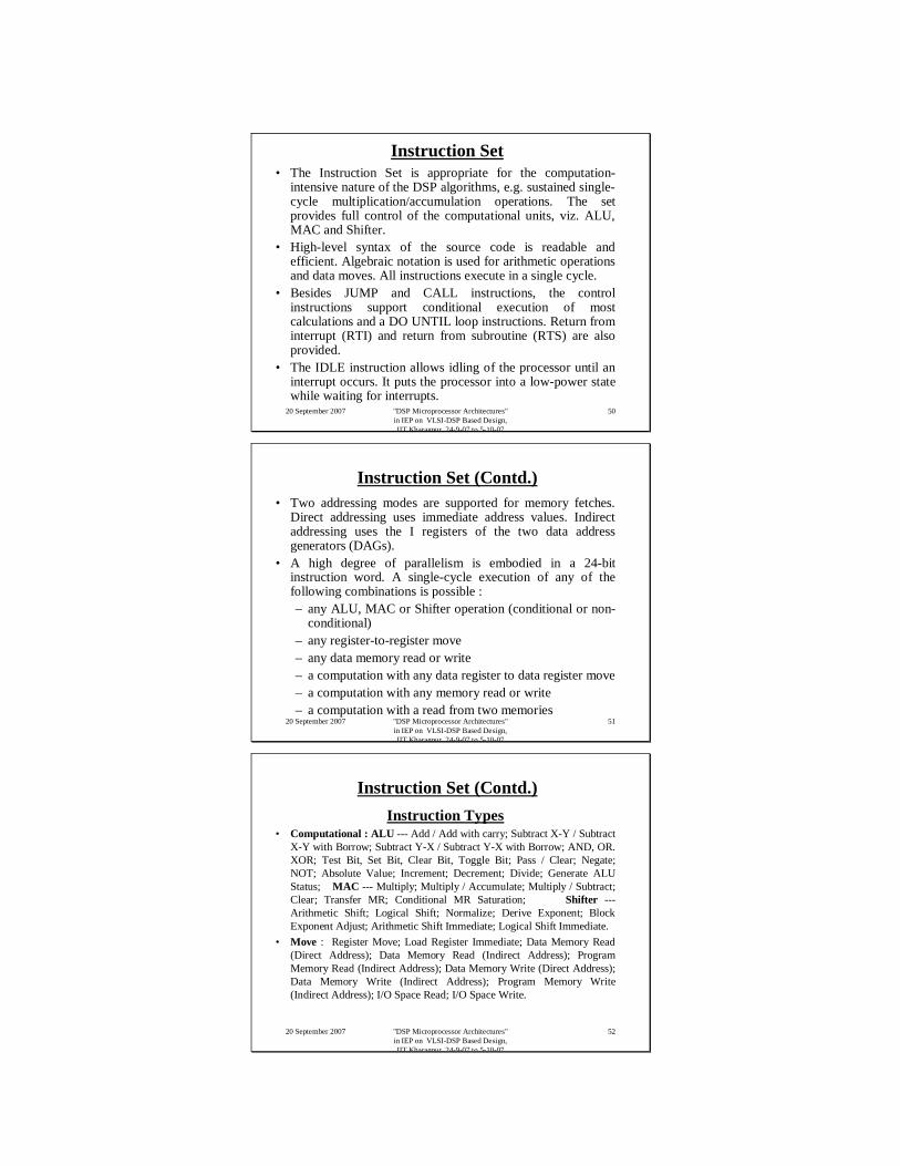
Instruction Set• The Instruction Set is appropriate for the computation-
intensive nature of the DSP algorithms, e.g. sustained single-cycle multiplication/accumulation operations. The set provides full control of the computational units, viz. ALU, MAC and Shifter.
• High-level syntax of the source code is readable and efficient. Algebraic notation is used for arithmetic operations and data moves. All instructions execute in a single cycle.
• Besides JUMP and CALL instructions, the control instructions support conditional execution of most calculations and a DO UNTIL loop instructions. Return from interrupt (RTI) and return from subroutine (RTS) are also provided.
• The IDLE instruction allows idling of the processor until an interrupt occurs. It puts the processor into a low-power state while waiting for interrupts.
20 September 2007 "DSP Microprocessor Architectures" in IEP on VLSI-DSP Based Design, IIT Kharagpur 24-9-07 to 5-10-07
51
Instruction Set (Contd.)• Two addressing modes are supported for memory fetches.
Direct addressing uses immediate address values. Indirect addressing uses the I registers of the two data address generators (DAGs).
• A high degree of parallelism is embodied in a 24-bit instruction word. A single-cycle execution of any of the following combinations is possible : – any ALU, MAC or Shifter operation (conditional or non-
conditional)– any register-to-register move– any data memory read or write– a computation with any data register to data register move – a computation with any memory read or write– a computation with a read from two memories
20 September 2007 "DSP Microprocessor Architectures" in IEP on VLSI-DSP Based Design, IIT Kharagpur 24-9-07 to 5-10-07
52
Instruction Set (Contd.)Instruction Types
• Computational : ALU --- Add / Add with carry; Subtract X-Y / Subtract X-Y with Borrow; Subtract Y-X / Subtract Y-X with Borrow; AND, OR. XOR; Test Bit, Set Bit, Clear Bit, Toggle Bit; Pass / Clear; Negate; NOT; Absolute Value; Increment; Decrement; Divide; Generate ALU Status; MAC --- Multiply; Multiply / Accumulate; Multiply / Subtract; Clear; Transfer MR; Conditional MR Saturation; Shifter ---Arithmetic Shift; Logical Shift; Normalize; Derive Exponent; Block Exponent Adjust; Arithmetic Shift Immediate; Logical Shift Immediate.
• Move : Register Move; Load Register Immediate; Data Memory Read (Direct Address); Data Memory Read (Indirect Address); Program Memory Read (Indirect Address); Data Memory Write (Direct Address); Data Memory Write (Indirect Address); Program Memory Write (Indirect Address); I/O Space Read; I/O Space Write.

20 September 2007 "DSP Microprocessor Architectures" in IEP on VLSI-DSP Based Design, IIT Kharagpur 24-9-07 to 5-10-07
53
Instruction Set (Contd.)Instruction Types (Contd.)
• Program Flow : JUMP, CALL, JUMP or CALL on Flag In Pin, Modify Flag Out Pin, Return from Subroutine, Return from Interrupt, Do Until, IDLE
• Miscellaneous : Stack Control, Mode Control, Modify Address Register, NOP, Interrupt Enable & Disable
• Multi-function : ALU/MAC/SHIFT with Memory Read, ALU/MAC/SHIFT with Data Register Move, ALU/MAC/SHIFT with Memory Write, Data & Program Memory Read, ALU/MAC with Data & Program Memory Read– It may be noted that the multi-function operations take advantage of
the inherent parallelism of the ADSP-2181 architecture by providing combinations of data moves, memory reads / memory writes, and computation, all in a single cycle.
20 September 2007 "DSP Microprocessor Architectures" in IEP on VLSI-DSP Based Design, IIT Kharagpur 24-9-07 to 5-10-07
54
Instruction Set (Contd.)Examples of Multi-function Instructions
• ALU/MAC with Data and Program Memory Read : The single most common operation in DSP algorithms is the sum of products, performed as :– Fetch two operands (such as a coefficient and a data point)– Multiply the operands and sum the result with previous products– Both the data fetch and the multiplication/accumulation can be
executed in a single cycle. An example of such an instruction is :MR = MR + MX0 * MY0 (SS), MX0=DM(I0,M0),MY0=PM(I4,M5);
• Computation with Memory Read --- allowed computations include all ALU operations except division, all Mac operations and all shifter operations except SHIFT IMMEDIATE. Computation must be unconditional. For example,
AR = AX0 + AY0, AX0 = DM (I0, M3);
• Computation with Data Register Move --- this instruction performs a data register to data register move in parallel with a computation. For example,
AR = AX0 + AY0, AX0 = MR2;
20 September 2007 "DSP Microprocessor Architectures" in IEP on VLSI-DSP Based Design, IIT Kharagpur 24-9-07 to 5-10-07
55
Program ExampleAn FIR filter program that exhibits much of the usefulness of the ADSP-2181 architecture and instruction set./**Beginning of Setup and Main Loop Routine**/
{ADSP FIR Filter Routine– Serial port 0 used for I/O– Internally generated serial clock– 12.288 MHz processor clock rate is divided to1.536 MHz serial clock– Serial clock divided to 8 KHz frame sampling rate}
.MODULE/RAM/ABS=0 main_routine; {program loaded from} { EPRwith MMAP=0}
A .INCLUDE <const.h>;B .VAR/DM/RAM/ABS=0x3800/CIRC data_buffer[taps]; {on-chip data
buffer} .VAR/PM/RAM/CIRC coefficient[taps];.GLOBAL data_buffer, coefficient;.EXTERNAL fir_start;.INIT coefficient:<coeff.dat>;
OM,
20 September 2007 "DSP Microprocessor Architectures" in IEP on VLSI-DSP Based Design, IIT Kharagpur 24-9-07 to 5-10-07
56
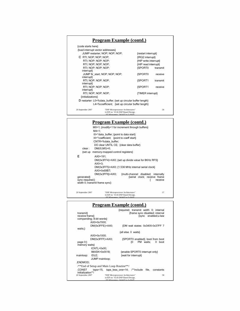
Program Example (contd.){code starts here}{load interrupt vector addresses}
JUMP restarter; NOP; NOP; NOP; {restart interrupt}
C RTI; NOP; NOP; NOP; {IRQ2 interrupt}RTI; NOP; NOP; NOP; {HIP write interrupt}RTI; NOP; NOP; NOP; {HIP read interrupt}RTI; NOP; NOP; NOP; {SPORT0 transmit
interrupt}JUMP fir_start; NOP; NOP; NOP; {SPORT0 receive
interrupt}RTI; NOP; NOP; NOP; {SPORT1 transmit
interrupt}RTI; NOP; NOP; NOP; {SPORT1 receive
interrupt}RTI; NOP; NOP; NOP; {TIMER interrupt}
{initializations}
D restarter: L0=%data_buffer; {set up circular buffer length}L4=%coefficient; {set up circular buffer length}
20 September 2007 "DSP Microprocessor Architectures" in IEP on VLSI-DSP Based Design, IIT Kharagpur 24-9-07 to 5-10-07
57
Program Example (contd.)M0=1; {modify=1 for increment through buffers}M4=1;I0=^data_buffer; {point to data start}I4=^coefficient; {point to coeff start}CNTR=%data_buffer;DO clear UNTIL CE; {clear data buffer}
clear : DM(I0,M0)=0;{set up memory-mapped control registers}
E AX0=191;DM(0x3FF4)=AX0; {set up divide value for 8KHz RFS}AX0=3;DM(0x3FF5)=AX0; {1.536 MHz internal serial clock}AX0=0x69B7;DM(0x3FF6}=AX0; {multi-channel disabled; internally
generated} {serial clock; receive frame sync required;} { receive width 0; transmit frame sync}
20 September 2007 "DSP Microprocessor Architectures" in IEP on VLSI-DSP Based Design, IIT Kharagpur 24-9-07 to 5-10-07
58
Program Example (contd.){required; transmit width 0; internal
transmit} {frame sync disabled; internal receive frame} {sync enabled;u-law companding; 8-bit words}
AX0=0x7000;DM(0x3FFE)=AX0; {DM wait states: 0x3400-0x37FF 7
waits;}{all else 0 waits}
AX0=0x1000; DM(0x3FFF)=AX0; {SPORT0 enabled}; boot from boot
page 0;} {0 PM waits; 0 boot memory waits}
ICNTL=0x00;IMASK=0x0018; {enable SPORT0 interrupt only}
mainloop: IDLE; {wait for interrupt}JUMP mainloop;
.ENDMOD;
/**End of Setup and Main Loop Routine**/.CONST taps=15, taps_less_one=14; /**include file, constants initialization**/
20 September 2007 "DSP Microprocessor Architectures" in IEP on VLSI-DSP Based Design, IIT Kharagpur 24-9-07 to 5-10-07
59
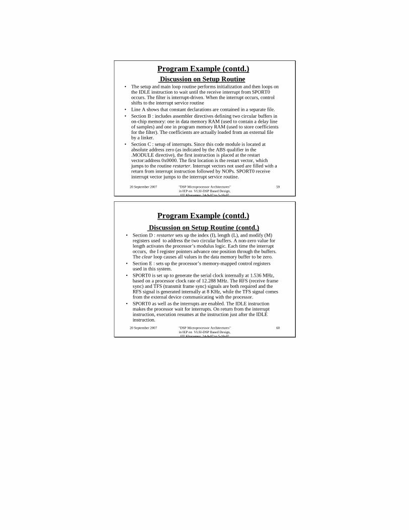
Program Example (contd.)Discussion on Setup Routine
• The setup and main loop routine performs initialization and then loops on the IDLE instruction to wait until the receive interrupt from SPORT0 occurs. The filter is interrupt-driven. When the interrupt occurs, control shifts to the interrupt service routine
• Line A shows that constant declarations are contained in a separate file.• Section B : includes assembler directives defining two circular buffers in
on-chip memory: one in data memory RAM (used to contain a delay line of samples) and one in program memory RAM (used to store coefficients for the filter). The coefficients are actually loaded from an external file by a linker.
• Section C : setup of interrupts. Since this code module is located at absolute address zero (as indicated by the ABS qualifier in the .MODULE directive), the first instruction is placed at the restart vector:address 0x0000. The first location is the restart vector, which jumps to the routine restarter. Interrupt vectors not used are filled with a return from interrupt instruction followed by NOPs. SPORT0 receive interrupt vector jumps to the interrupt service routine.
20 September 2007 "DSP Microprocessor Architectures" in IEP on VLSI-DSP Based Design, IIT Kharagpur 24-9-07 to 5-10-07
60
Program Example (contd.)Discussion on Setup Routine (contd.)
• Section D : restarter sets up the index (I), length (L), and modify (M) registers used to address the two circular buffers. A non-zero value for length activates the processor’s modulus logic. Each time the interrupt occurs, the I register pointers advance one position through the buffers. The clear loop causes all values in the data memory buffer to be zero.
• Section E : sets up the processor’s memory-mapped control registers used in this system.
• SPORT0 is set up to generate the serial clock internally at 1.536 MHz, based on a processor clock rate of 12.288 MHz. The RFS (receive frame sync) and TFS (transmit frame sync) signals are both required and the RFS signal is generated internally at 8 KHz, while the TFS signal comes from the external device communicating with the processor.
• SPORT0 as well as the interrupts are enabled. The IDLE instruction makes the processor wait for interrupts. On return from the interrupt instruction, execution resumes at the instruction just after the IDLE instruction.
20 September 2007 "DSP Microprocessor Architectures" in IEP on VLSI-DSP Based Design, IIT Kharagpur 24-9-07 to 5-10-07
61
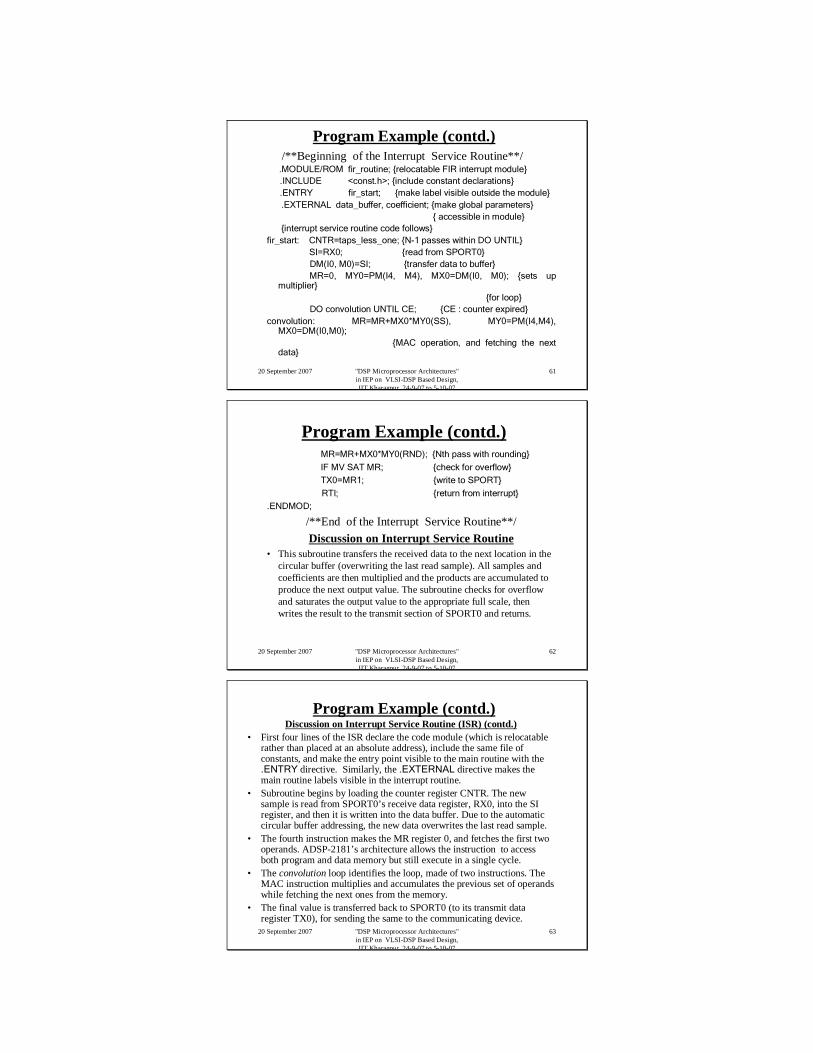
Program Example (contd.)/**Beginning of the Interrupt Service Routine**/
.MODULE/ROM fir_routine; {relocatable FIR interrupt module}.INCLUDE <const.h>; {include constant declarations}.ENTRY fir_start; {make label visible outside the module}.EXTERNAL data_buffer, coefficient; {make global parameters}
{ accessible in module}{interrupt service routine code follows}
fir_start: CNTR=taps_less_one; {N-1 passes within DO UNTIL}SI=RX0; {read from SPORT0}DM(I0, M0)=SI; {transfer data to buffer}MR=0, MY0=PM(I4, M4), MX0=DM(I0, M0); {sets up
multiplier}{for loop}
DO convolution UNTIL CE; {CE : counter expired}convolution: MR=MR+MX0*MY0(SS), MY0=PM(I4,M4),
MX0=DM(I0,M0);{MAC operation, and fetching the next
data}
20 September 2007 "DSP Microprocessor Architectures" in IEP on VLSI-DSP Based Design, IIT Kharagpur 24-9-07 to 5-10-07
62
Program Example (contd.)MR=MR+MX0*MY0(RND); {Nth pass with rounding}
IF MV SAT MR; {check for overflow}
TX0=MR1; {write to SPORT}
RTI; {return from interrupt}
.ENDMOD;
/**End of the Interrupt Service Routine**/Discussion on Interrupt Service Routine
• This subroutine transfers the received data to the next location in the circular buffer (overwriting the last read sample). All samples and coefficients are then multiplied and the products are accumulated to produce the next output value. The subroutine checks for overflow and saturates the output value to the appropriate full scale, then writes the result to the transmit section of SPORT0 and returns.
20 September 2007 "DSP Microprocessor Architectures" in IEP on VLSI-DSP Based Design, IIT Kharagpur 24-9-07 to 5-10-07
63
Program Example (contd.)Discussion on Interrupt Service Routine (ISR) (contd.)
• First four lines of the ISR declare the code module (which is relocatablerather than placed at an absolute address), include the same file of constants, and make the entry point visible to the main routine with the .ENTRY directive. Similarly, the .EXTERNAL directive makes the main routine labels visible in the interrupt routine.
• Subroutine begins by loading the counter register CNTR. The new sample is read from SPORT0’s receive data register, RX0, into the SI register, and then it is written into the data buffer. Due to the automatic circular buffer addressing, the new data overwrites the last read sample.
• The fourth instruction makes the MR register 0, and fetches the first two operands. ADSP-2181’s architecture allows the instruction to access both program and data memory but still execute in a single cycle.
• The convolution loop identifies the loop, made of two instructions. The MAC instruction multiplies and accumulates the previous set of operands while fetching the next ones from the memory.
• The final value is transferred back to SPORT0 (to its transmit data register TX0), for sending the same to the communicating device.
20 September 2007 "DSP Microprocessor Architectures" in IEP on VLSI-DSP Based Design, IIT Kharagpur 24-9-07 to 5-10-07
64
TMS320C54xTM DSPA fixed-point digital signal processor (DSP) in
TMS320TM DSP family
C54xTM DSP meets the need of embedded applications like telecommunications
High system performance of C54x is due to
Modified Harvard architecture
Minimized power consumption
High degree of parallelism
Versatile addressing modes and instruction set
20 September 2007 "DSP Microprocessor Architectures" in IEP on VLSI-DSP Based Design, IIT Kharagpur 24-9-07 to 5-10-07
65
Key Features of C54x DSPsCPU
one program bus, three data buses and four address buses
40-bit ALU (including 40-bit barrel shifter and two independent 40-bit accumulators)
17-bit by 17-bit multiplier coupled to a 40-bit adder for single-cycle multiply-accumulate (MAC) operation
compare, select, store unit (CCSU) for add-compare-selection of Viterbi operator
exponent encoder to compute exponent of 40-bit accumulator value in a single cycle
two address generators including 8 auxiliary registers
20 September 2007 "DSP Microprocessor Architectures" in IEP on VLSI-DSP Based Design, IIT Kharagpur 24-9-07 to 5-10-07
66
Key Features of C54x DSPs (contd.)Memory
192K words X 16-bit addressable memory space (64K-words program, 64K-words data and 64K-words I/O)
Instruction setSingle-instruction repeat and block repeat operations
Block memory move instructions for better program and data management
Instructions with 2- or 3-operand simultaneous reads
Arithmetic instructions with parallel store and parallel load
Fast return from interrupt

20 September 2007 "DSP Microprocessor Architectures" in IEP on VLSI-DSP Based Design, IIT Kharagpur 24-9-07 to 5-10-07
67
Key Features of C54x DSPs (contd.)On-chip peripherals
software-programmable wait-state generator
on-chip PLL clock generator
Programmable bank-switching logic
programmable timer
Ports (25 ns (40 MIPs) to 10 ns (100 MIPs)
PowerPower consumption control (power-down mode instructions
Control to disable CLKOUT signal
20 September 2007 "DSP Microprocessor Architectures" in IEP on VLSI-DSP Based Design, IIT Kharagpur 24-9-07 to 5-10-07
68
Architectural OverviewModified Harvard architecture with eight buses
Separate program and data spaces enable parallelism, e.g. 3 reads and 1 write in a single cycle
Data transfer between data and program spaces
Instructions with parallel store and application-specific instructions utilize this architecture
Parallelism supports a set of arithmetic, logic and bit-manipulation ops that can be done in a single cycle
C54x has control mechanisms for interrupts, repeated ops and function calling
20 September 2007 "DSP Microprocessor Architectures" in IEP on VLSI-DSP Based Design, IIT Kharagpur 24-9-07 to 5-10-07
69
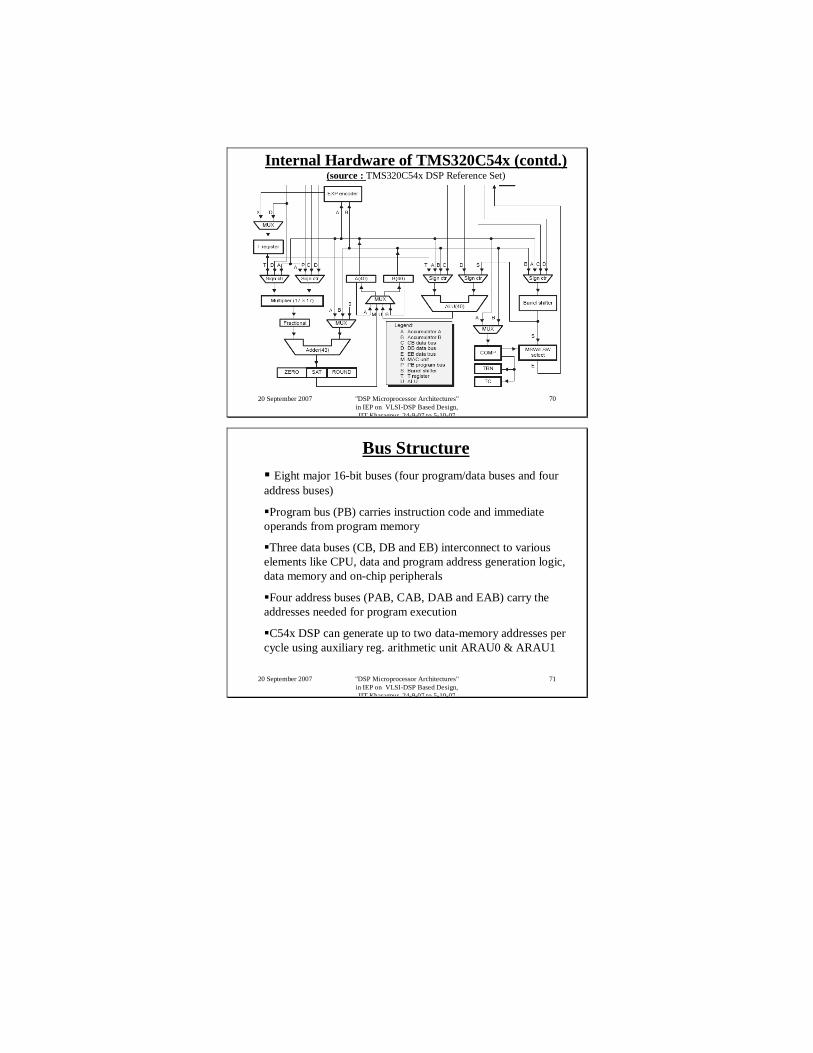
Internal Hardware of TMS320C54x (source : TMS320C54x DSP Reference Set)
20 September 2007 "DSP Microprocessor Architectures" in IEP on VLSI-DSP Based Design, IIT Kharagpur 24-9-07 to 5-10-07
70
Internal Hardware of TMS320C54x (contd.) (source : TMS320C54x DSP Reference Set)
20 September 2007 "DSP Microprocessor Architectures" in IEP on VLSI-DSP Based Design, IIT Kharagpur 24-9-07 to 5-10-07
71
Bus StructureEight major 16-bit buses (four program/data buses and four
address buses)
Program bus (PB) carries instruction code and immediate operands from program memory
Three data buses (CB, DB and EB) interconnect to various elements like CPU, data and program address generation logic, data memory and on-chip peripherals
Four address buses (PAB, CAB, DAB and EAB) carry the addresses needed for program execution
C54x DSP can generate up to two data-memory addresses per cycle using auxiliary reg. arithmetic unit ARAU0 & ARAU1

20 September 2007 "DSP Microprocessor Architectures" in IEP on VLSI-DSP Based Design, IIT Kharagpur 24-9-07 to 5-10-07
72
Internal Memory OrganizationC54x DSP memory space is organized into three individually
selectable space : program, data and I/O space
C54x devices can have RAM and ROM
Types of RAM : dual-access RAM (DARAM), single-access RAM (SARAM), and two-way shared RAM
DARAM and SARAM can be shared within subsystems of a multiple-CPU core device. These can be configured as data memory or program/data memory
In addition 26 CPU registers and peripheral registers are mapped in data memory space. Memory-mapped access gives easy means to save and restore registers for context switches and to transfer values between accumulator & other registers
20 September 2007 "DSP Microprocessor Architectures" in IEP on VLSI-DSP Based Design, IIT Kharagpur 24-9-07 to 5-10-07
73
ConclusionsDigital signal processors (DSPs) are key components
of consumer, communications and medical products
Specialized hardware and instructions make DSPsefficient at executing signal processing computations
Techniques to increase parallelism and clock speed of DSPs are developed for wireless communications and Internet audio/video applications
For many applications, speed is not the most important aspect of a processor’s performance. Minimizing system cost, power, memory capacity, application software, hardware development effort and risk is equally critical
20 September 2007 "DSP Microprocessor Architectures" in IEP on VLSI-DSP Based Design, IIT Kharagpur 24-9-07 to 5-10-07
74
References1. Madisetti, V.K., VLSI Digital Signal Processors,
IEEE Press, Butterworth Heinemann.2. Eyre, J., The Digital Signal Processor Derby, IEEE
Spectrum, June 20013. ADSP-2100 Family User’s Manual, 3rd edition,
Analog Devices, Inc.4. TMS320C54x DSP Reference Set, Vol. 1 : CPU and
Peripherals, Literature No. SPRU131G, Texas Instruments Inc.


![Experiencia I[1].E.C.E](https://img.dokumen.tips/doc/110x75/55a15b2c1a28ab3d0e8b48bd/experiencia-i1ece.jpg)