Embed Size (px)
Citation preview

G
0.6-V
Reference
Comparator
OUT
CMPIN
CMPOUT
VIN-
VIN+
INA200 (G = 20)INA201 (G = 50)
INA202 (G = 100)
RESET
GND
VS
2
3
4
6
5
7
8
1
Copyright © 2017, Texas Instruments Incorporated
Product
Folder
Order
Now
Technical
Documents
Tools &
Software
Support &Community
ReferenceDesign
An IMPORTANT NOTICE at the end of this data sheet addresses availability, warranty, changes, use in safety-critical applications,intellectual property matters and other important disclaimers. PRODUCTION DATA.
INA200, INA201, INA202SBOS374E –NOVEMBER 2006–REVISED SEPTEMBER 2017
INA20x High-Side Measurement Current-Shunt MonitorWith Open-Drain Comparator and Reference
1
1 Features1• Complete Current Sense Solution• Three Gain Options Available:
– INA200 = 20 V/V– INA201 = 50 V/V– INA202 = 100 V/V
• 0.6-V Internal Voltage Reference• Internal Open-Drain Comparator• Latching Capability on Comparator• Common-Mode Range: –16 V to 80 V• High Accuracy: 3.5% Maximum Error Over
Temperature• Bandwidth: 500 kHz (INA200)• Quiescent Current: 1800 μA (Maximum)• Packages: SOIC-8, VSSOP-8
2 Applications• Notebook Computers• Cell Phones• Telecom Equipment• Automotive• Power Management• Battery Chargers• Welding Equipment
3 DescriptionThe INA200, INA201, and INA202 devices are high-side current-shunt monitors with voltage output andintegrated comparator. The INA20x devices cansense drops across shunts at common-modevoltages from –16 V to 80 V. The INA20x series isavailable with three output voltage scales: 20 V/V, 50V/V, and 100 V/V, with a bandwidth up to 500-kHz.
The INA200, INA201, and INA202 devicesincorporate an open-drain comparator and internalreference providing a 0.6-V threshold. Externaldividers set the current trip point. The comparatorincludes a latching capability, that can be madetransparent by grounding (or leaving open) theRESET pin.
The INA200, INA201, and INA202 devices operatefrom a single 2.7-V to 18-V supply, drawing amaximum of 1800 μA of supply current. Packageoptions include the very small VSSOP-8 and theSOIC-8. All versions are specified over the extendedoperating temperature range of –40°C to +125°C.
Device Information(1)
PART NUMBER PACKAGE BODY SIZE (NOM)INA200INA201INA202
SOIC (8) 4.90 mm × 3.91 mm
VSSOP (8) 3.00 mm × 3.00 mm
(1) For all available packages, see the orderable addendum atthe end of the data sheet.
Simplified Schematic

2
INA200, INA201, INA202SBOS374E –NOVEMBER 2006–REVISED SEPTEMBER 2017 www.ti.com
Product Folder Links: INA200 INA201 INA202
Submit Documentation Feedback Copyright © 2006–2017, Texas Instruments Incorporated
Table of Contents1 Features .................................................................. 12 Applications ........................................................... 13 Description ............................................................. 14 Revision History..................................................... 25 Pin Configuration and Functions ......................... 36 Specifications......................................................... 4
6.1 Absolute Maximum Ratings ...................................... 46.2 ESD Ratings.............................................................. 46.3 Recommended Operating Conditions....................... 46.4 Thermal Information .................................................. 46.5 Electrical Characteristics: Current-Shunt Monitor ..... 56.6 Electrical Characteristics: Comparator...................... 76.7 Electrical Characteristics: General ............................ 76.8 Typical Characteristics .............................................. 9
7 Detailed Description ............................................ 137.1 Overview ................................................................. 137.2 Functional Block Diagram ....................................... 13
7.3 Feature Description................................................. 137.4 Device Functional Modes........................................ 19
8 Application and Implementation ........................ 228.1 Application Information............................................ 228.2 Typical Application ................................................. 22
9 Power Supply Recommendations ...................... 239.1 Output vs Supply Ramp Considerations................. 23
10 Layout................................................................... 2510.1 Layout Guidelines ................................................. 2510.2 Layout Example .................................................... 25
11 Device and Documentation Support ................. 2611.1 Related Links ........................................................ 2611.2 Community Resources.......................................... 2611.3 Trademarks ........................................................... 2611.4 Electrostatic Discharge Caution............................ 2611.5 Glossary ................................................................ 26
12 Mechanical, Packaging, and OrderableInformation ........................................................... 26
4 Revision HistoryNOTE: Page numbers for previous revisions may differ from page numbers in the current version.
Changes from Revision D (October 2015) to Revision E Page
• Reformatted Thermal Information table note ......................................................................................................................... 4• Corrected typo in Voltage Output section in Electrical Characteristics table ......................................................................... 6• Added text to Comparator subsection in Feature Description section ................................................................................. 14• Added Figure 31 to Feature Description section .................................................................................................................. 18• Added Output vs Supply Ramp Considerations subsection in Feature Description section................................................ 23• Added Figure 36, Figure 37, and Figure 38 ......................................................................................................................... 23
Changes from Revision C (October 2010) to Revision D Page
• Added ESD Ratings table, Thermal Information table, Feature Description section, Device Functional Modes,Application and Implementation section, Power Supply Recommendations section, Layout section, Device andDocumentation Support section, and Mechanical, Packaging, and Orderable Information section ..................................... 4
Changes from Revision B (October, 2007) to Revision C Page
• Revised front-page figure ....................................................................................................................................................... 1• Changed title of data sheet..................................................................................................................................................... 1• Updated document format to current standards..................................................................................................................... 1

1
2
3
4
8
7
6
5
VIN+
VIN-
CMPOUT
RESET
VS
OUT
CMPIN
GND
3
INA200, INA201, INA202www.ti.com SBOS374E –NOVEMBER 2006–REVISED SEPTEMBER 2017
Product Folder Links: INA200 INA201 INA202
Submit Documentation FeedbackCopyright © 2006–2017, Texas Instruments Incorporated
5 Pin Configuration and Functions
DGK and D Packages8-Pin VSSOP and SOIC
Top View
Pin FunctionsPIN
I/O DESCRIPTIONNAME NO.CMPIN 3 Analog input Comparator input
CMPOUT 6 Analogoutput Comparator output
GND 4 Analog Ground
OUT 2 Analogoutput Output voltage
RESET 5 Analog input Comparator reset pin, active lowVIN– 7 Analog input Connect to shunt low sideVIN+ 8 Analog input Connect to shunt high sideVS 1 Analog Power supply

4
INA200, INA201, INA202SBOS374E –NOVEMBER 2006–REVISED SEPTEMBER 2017 www.ti.com
Product Folder Links: INA200 INA201 INA202
Submit Documentation Feedback Copyright © 2006–2017, Texas Instruments Incorporated
(1) Stresses beyond those listed under Absolute Maximum Ratings may cause permanent damage to the device. These are stress ratingsonly, which do not imply functional operation of the device at these or any other conditions beyond those indicated under RecommendedOperating Conditions. Exposure to absolute-maximum-rated conditions for extended periods may affect device reliability.
(2) This voltage may exceed the ratings shown if the current at that pin is limited to 5 mA.
6 Specifications
6.1 Absolute Maximum Ratingsover operating free-air temperature range (unless otherwise noted) (1)
MIN MAX UNITSupply voltage, Vs 2.7 18 V
Current-shunt monitoranalog inputs, VIN+, VIN–
Differential (VIN+) – (VIN–) –18 18 VCommon-mode (2) –16 80 V
Comparator analog input and reset pins (2) GND – 0.3 (Vs) + 0.3 VAnalog output, OUT (2) GND – 0.3 (Vs) + 0.3 VComparator output, OUT (2) GND – 0.3 18 VInput current into any pin (2) 5 mAOperating temperature –55 150 °CJunction temperature –65 150 °CStorage temperature, Tstg –65 150 °C
(1) JEDEC document JEP155 states that 500-V HBM allows safe manufacturing with a standard ESD control process.(2) JEDEC document JEP157 states that 250-V CDM allows safe manufacturing with a standard ESD control process.
6.2 ESD RatingsVALUE UNIT
V(ESD) Electrostatic dischargeHuman body model (HBM), per ANSI/ESDA/JEDEC JS-001, all pins (1) ±4000
VCharged device model (CDM), per JEDEC specification JESD22-C101, allpins (2) ±1000
6.3 Recommended Operating Conditionsover operating free-air temperature range (unless otherwise noted)
MIN NOM MAX UNITVCM Common-mode input voltage –16 12 80 VVS Operating supply voltage 2.7 12 18 VTA Operating free-air temperature –40 25 125 °C
(1) For more information about traditional and new thermal metrics, see the Semiconductor and IC Package Thermal Metrics applicationreport.
6.4 Thermal Information
THERMAL METRIC (1)INA20x
UNITD (SOIC) DGK (SOIC)8 PINS 8 PINS
RθJA Junction-to-ambient thermal resistance 110.5 162.2 °C/WRθJC(top) Junction-to-case (top) thermal resistance 50.4 37.7 °C/WRθJB Junction-to-board thermal resistance 52.7 82.9 °C/WψJT Junction-to-top characterization parameter 7.8 1.3 °C/WψJB Junction-to-board characterization parameter 51.9 81.4 °C/W

5
INA200, INA201, INA202www.ti.com SBOS374E –NOVEMBER 2006–REVISED SEPTEMBER 2017
Product Folder Links: INA200 INA201 INA202
Submit Documentation FeedbackCopyright © 2006–2017, Texas Instruments Incorporated
(1) Offset is extrapolated from measurements of the output at 20-mV and 100-mV VSENSE.
6.5 Electrical Characteristics: Current-Shunt Monitorat TA = 25°C, VS = 12 V, VCM = 12 V, VSENSE = 100 mV, RL = 10 kΩ to GND, RPULL-UP = 5.1 kΩ connected from CMPOUT to VS,and CMPIN = GND, (unless otherwise noted)
PARAMETER TEST CONDITIONS MIN TYP MAX UNIT
INPUT
VSENSE Full-scale sense input voltage VSENSE = VIN+ – VIN– 0.15 (VS – 0.25) / Gain V
VCM Common-mode input range TA = –40°C to 125°C –16 80 V
CMR Common-mode rejectionVIN+ = –16 V to 80 V 80 100 dB
VIN+ = 12 V to 80 V, TA = –40°C to 125°C 100 123 dB
VOS Offset voltage, RTI (1)
TA = 25°C ±0.5 ±2.5 mV
TA = 25°C to 125°C ±3 mV
TA = –40°C to 25°C ±3.5 mV
dVOS/dT Offset voltage, RTI, vstemperature TMIN to TMAX, TA = –40°C to 125°C 5 μV/°C
PSR Offset voltage, RTI, vs powersupply
VOUT = 2 V, VIN+ = 18 V, 2.7 V, TA = –40°C to125°C 2.5 100 μV/V
IB Input bias current, VIN– pin TA = –40°C to 125°C ±9 ±16 μA

6
INA200, INA201, INA202SBOS374E –NOVEMBER 2006–REVISED SEPTEMBER 2017 www.ti.com
Product Folder Links: INA200 INA201 INA202
Submit Documentation Feedback Copyright © 2006–2017, Texas Instruments Incorporated
Electrical Characteristics: Current-Shunt Monitor (continued)at TA = 25°C, VS = 12 V, VCM = 12 V, VSENSE = 100 mV, RL = 10 kΩ to GND, RPULL-UP = 5.1 kΩ connected from CMPOUT to VS,and CMPIN = GND, (unless otherwise noted)
PARAMETER TEST CONDITIONS MIN TYP MAX UNIT
(2) Total output error includes effects of gain error and VOS.(3) Linearity is best fit to a straight line.(4) For details on this region of operation, see Accuracy Variations section in Device Functional Modes.(5) See Figure 8.(6) Specified by design.
OUTPUT (VSENSE ≥ 20 mV)
G Gain
INA200 20 V/V
INA201 50 V/V
INA202 100 V/V
Gain errorVSENSE = 20 mV to 100 mV ±0.2% ±1%
VSENSE = 20 mV to 100 mV, TA = –40°C to125°C ±2%
Total output error (2)VSENSE = 120 mV, VS = 16 V ±0.75% ±2.2%
VSENSE = 120 mV, VS = 16 V, TA = –40°C to125°C ±3.5%
Nonlinearity error (3) VSENSE = 20 mV to 100 mV ±0.002%
RO Output impedance 1.5 Ω
Maximum capacitive load No sustained oscillation 10 nF
OUTPUT (VSENSE < 20 mV) (4)
Output
INA200, INA201,INA202 –16 V ≤ VCM < 0 V 300 mV
INA200 0 V ≤ VCM ≤ VS, VS =5 V 0.4 V
INA201 0 V ≤ VCM ≤ VS, VS =5 V 1 V
INA202 0 V ≤ VCM ≤ VS, VS =5 V 2 V
INA200, INA201,INA202 VS < VCM ≤ 80 V 300 mV
VOLTAGE OUTPUT (5)
Output swing to the positive rail VIN– = 11 V, VIN+ = 12 V, TA = –40°C to 125°C (Vs) – 0.15 (Vs) – 0.25 V
Output swing to GND (6) VIN– = 0 V, VIN+ = –0.5 V, TA = –40°C to 125°C (GND) + 0.004 (GND) + 0.05 V
FREQUENCY RESPONSE
BW Bandwidth
INA200 CLOAD = 5 pF 500 kHz
INA201 CLOAD = 5 pF 300 kHz
INA202 CLOAD = 5 pF 200 kHz
Phase margin CLOAD < 10 nF 40 °C
SR Slew rate 1 V/μs
Settling time (1%) VSENSE = 10 mVPP to 100 mVPP,CLOAD = 5 pF 2 μs
NOISE, RTI
Voltage noise density 40 nV/√Hz

7
INA200, INA201, INA202www.ti.com SBOS374E –NOVEMBER 2006–REVISED SEPTEMBER 2017
Product Folder Links: INA200 INA201 INA202
Submit Documentation FeedbackCopyright © 2006–2017, Texas Instruments Incorporated
(1) Hysteresis refers to the threshold (the threshold specification applies to a rising edge of a noninverting input) of a falling edge on thenoninverting input of the comparator; refer to Figure 1.
(2) Specified by design.(3) VID refers to the differential voltage at the comparator inputs.(4) Open-drain output can be pulled to the range of 2.7 to 18 V, regardless of VS.(5) The comparator response time specified is the interval between the input step function and the instant when the output crosses 1.4 V.(6) The RESET input has an internal 2 MΩ (typical) pull-down. Leaving RESET open results in a LOW state, with transparent comparator
operation.
6.6 Electrical Characteristics: Comparatorat TA = 25°C, VS = 12 V, VCM = 12 V, VSENSE = 100 mV, RL = 10 kΩ to GND, and RPULL-UP = 5.1 kΩ connected from CMPOUT toVS, (unless otherwise noted)
PARAMETER TEST CONDITIONS MIN TYP MAX UNIT
OFFSET VOLTAGE
ThresholdTA = 25°C 590 608 620 mV
TA = –40°C to 125°C 586 625 mV
Hysteresis (1) TA = –40°C to 85°C –8 mV
INPUT BIAS CURRENT (2)
Input bias current, CMPin PIN 0.005 10 nA
Input bias current, CMPin PIN, vs temperature TA = –40°C to 125°C 15 nA
INPUT VOLTAGE RANGE
Input voltage range, CMPin PIN 0 V to VS – 1.5 V V
OUTPUT (OPEN-DRAIN)
Large-signal differential voltage gain CMP VOUT 1 V to 4 V,RL ≥ 15 kΩ connected to 5 V 200 V/mV
ILKG High-level leakage current (3) (4) VID = 0.4 V, VOH = VS 0.0001 1 μA
VOL Low-level output voltage (3) VID = –0.6 V, IOL = 2.35 mA 220 300 mV
RESPONSE TIME
Response time (5) RL to 5 V, CL = 15 pF, 100-mV InputStep with 5-mV overdrive 1.3 μs
RESET
RESET threshold (6) 1.1 V
Logic input impedance 2 MΩ
Minimum RESET pulse width 1.5 μs
RESET propagation delay 3 μs
(1) The INA200, INA201, and INA202 are designed to power-up with the comparator in a defined reset state as long as RESET is open orgrounded. The comparator is in reset as long as the power supply is below the voltage shown here. The comparator assumes a statebased on the comparator input above this supply voltage. If RESET is high at power-up, the comparator output comes up high andrequires a reset to assume a low state, if appropriate.
6.7 Electrical Characteristics: Generalat TA = 25°C, VS = 12 V, VCM = 12 V, VSENSE = 100 mV, RL = 10 kΩ to GND, RPULL-UP = 5.1 kΩ connected from CMPOUT to VS,and CMPIN = 1 V, unless otherwise noted.
PARAMETER TEST CONDITIONS MIN TYP MAX UNIT
POWER SUPPLY
VS Operating power supply TA = –40°C to 125°C 2.7 18 V
IQ Quiescent currentVOUT = 2 V 1350 1800 μA
VSENSE = 0 mV, TA = –40°C to 125°C 1850 μA
Comparator power-on resetthreshold (1) 1.5 V
TEMPERATURE
Specified temperature –40 125 °C
Operating temperature –55 150 °C
Storage temperature –65 150 °C
θJA Thermal resistanceVSSOP-8 Surface-Mount 200 °C/W
SOIC-8 150 °C/W

Hysteresis = V 8mV-THRESHOLD
VTHRESHOLD
Input Voltage
0.6V0.592V
8
INA200, INA201, INA202SBOS374E –NOVEMBER 2006–REVISED SEPTEMBER 2017 www.ti.com
Product Folder Links: INA200 INA201 INA202
Submit Documentation Feedback Copyright © 2006–2017, Texas Instruments Incorporated
Figure 1. Typical Comparator Hysteresis

0.1
0.09
0.08
0.07
0.06
0.05
0.04
0.03
0.02
0.01
0-16 -12 -8 -4 0 4 128 2016
Ou
tpu
t E
rro
r (%
)
Common-Mode Voltage (V)
... 76 80
4.0
3.5
3.0
2.5
2.0
1.5
1.0
0.5
0
0 50 100 150 200 250 300 350
Ou
tpu
t E
rro
r
(% e
rro
r o
f th
e id
ea
l o
utp
ut
va
lue
)
V (mV)SENSE
400 450 500
20
18
16
14
12
10
8
6
4
2
0
20 100 200 300 400 500 600 700
V(V
)O
UT
V (mV)DIFFERENTIAL
800 900
50V/V
20V/V
100V/V
140
130
120
110
100
90
80
70
60
50
40
10 100 1k 10k
Co
mm
on
-Mo
de
an
d
Po
we
r-S
up
ply
Re
jectio
n (
dB
)
Frequency (Hz)
100k
CMR
PSR
45
40
35
30
25
20
15
10
510k 100k
Ga
in (
dB
)
Frequency (Hz)
1M
G = 100 C = 1000pFLOAD
G = 50
G = 20
45
40
35
30
25
20
15
10
510k 100k
Ga
in (
dB
)
Frequency (Hz)
1M
G = 100
G = 50
G = 20
9
INA200, INA201, INA202www.ti.com SBOS374E –NOVEMBER 2006–REVISED SEPTEMBER 2017
Product Folder Links: INA200 INA201 INA202
Submit Documentation FeedbackCopyright © 2006–2017, Texas Instruments Incorporated
6.8 Typical Characteristicsat TA = 25°C, VS = 12 V, VIN+ = 12 V, and VSENSE = 100 mV, (unless otherwise noted)
Figure 2. Gain vs Frequency Figure 3. Gain vs Frequency
Figure 4. Gain Plot Figure 5. Common-Mode and Power-Supply Rejection vsFrequency
Figure 6. Output Error vs VSENSE Figure 7. Output Error vs Common-Mode Voltage

Ou
tpu
t V
olta
ge
(5
0m
V/d
iv)
Time (2 s/div)m
G = 20
V = 20mV to 30mVSENSE
Time (2 s/div)m
G = 20
Ou
tpu
t V
olta
ge
(5
00
mV
/div
)
V = 20mV to 110mVSENSE
34
30
26
22
18
14
10
6
2.5 3.5 4.5 5.5 6.5 7.5 8.5 9.5 10.5
Outp
ut S
hort
-Circuit C
urr
ent (m
A)
Supply Voltage (V)
11.5 17 18
- °40 C
+ °25 C
+125 C°
2.00
1.75
1.50
1.25
1.00
0.75
0.50
-16 -12 -8 -4 0 4 8 12 16 20 24 28
I(m
A)
Q
V (V)CM
32 36
V = 0mVSENSE
V = 12VS
V = 2.7VS
V = 100mVSENSE
V = 12VSV = 2.7VS
12
11
10
9
8
7
6
5
4
3
2
1
00 5 10 15 20
Ou
tpu
t V
olta
ge
(V
)
Output Current (mA)
25 30
V = 12VS
+25 C°
+25 C°
- °40 C
- °40 C
+125 C°
+125 C°
Sourcing Current
V = 3VS
Sourcing Current
Output stage is designed
to source current. Current
sinking capability is
approximately 400 A.m
3.5
3.0
2.5
2.0
1.5
1.0
0.5
0
0 1 2 3 4 5 6 7
I(m
A)
Q
Output Voltage (V)
8 9 10
10
INA200, INA201, INA202SBOS374E –NOVEMBER 2006–REVISED SEPTEMBER 2017 www.ti.com
Product Folder Links: INA200 INA201 INA202
Submit Documentation Feedback Copyright © 2006–2017, Texas Instruments Incorporated
Typical Characteristics (continued)at TA = 25°C, VS = 12 V, VIN+ = 12 V, and VSENSE = 100 mV, (unless otherwise noted)
Figure 8. Positive Output Voltage Swing vs Output Current Figure 9. Quiescent Current vs Output Voltage
Figure 10. Quiescent Current vs Common-Mode Voltage Figure 11. Output Short-Circuit Current vs Supply Voltage
Figure 12. Step Response Figure 13. Step Response
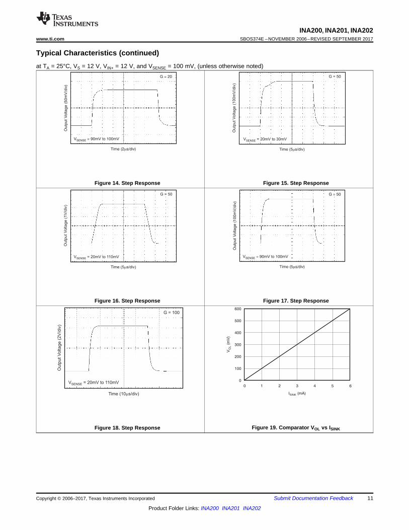
Time (10 s/div)m
G = 100
Outp
ut V
oltage (
2V
/div
)
V = 20mV to 110mVSENSE
600
500
400
300
200
100
0
0 1 2 3 4 5
V(m
V)
OL
I (mA)SINK
6
Time (5 s/div)m
G = 50
Outp
ut V
oltage (
1V
/div
)
V = 20mV to 110mVSENSE
Time (5 s/div)m
G = 50
Ou
tpu
t V
olta
ge
(1
00
mV
/div
)
V = 90mV to 100mVSENSE
Time (2 s/div)m
G = 20
Ou
tpu
t V
olta
ge
(5
0m
V/d
iv)
V = 90mV to 100mVSENSE
Time (5 s/div)m
G = 50
Outp
ut V
oltage (
100m
V/d
iv)
V = 20mV to 30mVSENSE
11
INA200, INA201, INA202www.ti.com SBOS374E –NOVEMBER 2006–REVISED SEPTEMBER 2017
Product Folder Links: INA200 INA201 INA202
Submit Documentation FeedbackCopyright © 2006–2017, Texas Instruments Incorporated
Typical Characteristics (continued)at TA = 25°C, VS = 12 V, VIN+ = 12 V, and VSENSE = 100 mV, (unless otherwise noted)
Figure 14. Step Response Figure 15. Step Response
Figure 16. Step Response Figure 17. Step Response
Figure 18. Step Response Figure 19. Comparator VOL vs ISINK

Input
200mV/div
Output
2V/div
2 s/divm
V = 5mVOD
300
275
250
225
200
175
150
125
-50 -25 0 25 50 75 100
Pro
pagation D
ela
y (
ns)
Temperature ( C)°
125
200
175
150
125
100
75
50
0 20 40 60 80 100 120 140 160 180
Pro
pa
ga
tio
n D
ela
y (
ns)
Overdrive Voltage (mV)
200
1.2
1.0
0.8
0.6
0.4
0.2
0
2 4 6 8 10 12 14 16
Re
se
t V
olta
ge
(V
)
Supply Voltage (V)
18
600
599
598
597
596
595
594
593
592
591
5902 4 6 8 10 12 14 16
Re
se
t V
olta
ge
(m
V)
Supply Voltage (V)
18
602
601
600
599
598
597
596
-50 -25 0 25 50 75 100
Co
mp
ara
tor
Trip
Po
int
(mV
)
Temperature ( C)°
125
12
INA200, INA201, INA202SBOS374E –NOVEMBER 2006–REVISED SEPTEMBER 2017 www.ti.com
Product Folder Links: INA200 INA201 INA202
Submit Documentation Feedback Copyright © 2006–2017, Texas Instruments Incorporated
Typical Characteristics (continued)at TA = 25°C, VS = 12 V, VIN+ = 12 V, and VSENSE = 100 mV, (unless otherwise noted)
Figure 20. Comparator Trip Point vs Supply Voltage Figure 21. Comparator Trip Point vs Temperature
Figure 22. Comparator Propagation Delay vs OverdriveVoltage
Figure 23. Comparator Reset Voltage vs Supply Voltage
Figure 24. Comparator Propagation Delay vs Temperature Figure 25. Comparator Propagation Delay

G
0.6-VReference
Comparator
OUT
RESETGND
VS
CMPOUT
VIN+
VIN-
CMPIN
13
INA200, INA201, INA202www.ti.com SBOS374E –NOVEMBER 2006–REVISED SEPTEMBER 2017
Product Folder Links: INA200 INA201 INA202
Submit Documentation FeedbackCopyright © 2006–2017, Texas Instruments Incorporated
7 Detailed Description
7.1 OverviewThe INA200, INA201, and INA202 devices are high-side current-shunt monitors with voltage output. The INA20xdevices can sense drops across shunts at common-mode voltages from –16 V to 80 V. The INA200–INA202devices are available with three output voltage scales: 20 V/V, 50 V/V, and 100 V/V, with up to 500-kHzbandwidth. The INA200, INA201, and INA202 devices incorporate an open-drain comparator and internalreference providing a 0.6-V threshold. External dividers set the current trip point. The comparator includes alatching capability, that can be made transparent by grounding (or leaving open) the RESET pin. The INA200,INA201, and INA202 devices operate from a single 2.7 to 18-V supply, drawing a maximum of 1800 μA of supplycurrent. Package options include the very small MSOP-8 and the SO-8. All versions are specified over theextended operating temperature range of –40°C to +125°C.
7.2 Functional Block Diagram
7.3 Feature Description
7.3.1 Basic ConnectionsFigure 26 shows the basic connections of the INA20x devices. The input pins (VIN+ and VIN–) must be connectedas closely as possible with Kelvin connections to the shunt resistor to minimize any resistance in series with theshunt resistance.
Power-supply bypass capacitors are required for stability. Applications with noisy or high-impedance powersupplies may require additional decoupling capacitors to reject power-supply noise. Connect bypass capacitorsclose to the device pins.

G
Comparator
INA200(G = 20)
2
3
4
6
5
7
8
1
Latch
Transparent / Reset
Load
5-V Supply
0.6-VReference
RESET
CMPOUT
VIN+
VIN-
OUT
GND
CMPIN
VS
R2
R1CBYPASS 0.01 µF
SW
RSHUNT 3 m Load Supply
-18 V to 80 V
RPULLUP
4.7 k
Copyright © 2017, Texas Instruments Incorporated
14
INA200, INA201, INA202SBOS374E –NOVEMBER 2006–REVISED SEPTEMBER 2017 www.ti.com
Product Folder Links: INA200 INA201 INA202
Submit Documentation Feedback Copyright © 2006–2017, Texas Instruments Incorporated
Figure 26. INA200 Basic Connections
7.3.2 Selecting RS
The selected value for the shunt resistor, RS, depends on the application and is a compromise between small-signal accuracy and maximum permissible voltage loss in the measurement line. High values of RS provide betteraccuracy at lower currents by minimizing the effects of offset, while low values of RS minimize voltage loss in thesupply line. For most applications, using an RS value that provides a full-scale shunt voltage range of 50 mV to100 mV results in the best performance. Maximum input voltage for accurate measurements is 500 mV, butoutput voltage is limited by supply.
7.3.3 ComparatorThe INA200, INA201, and INA202 devices incorporate an open-drain comparator. This comparator typically has2 mV of offset and a 1.3-μs (typical) response time. The output of the comparator latches and is reset throughthe RESET pin; see Figure 28.
When Vs and RESET are different, TI recommends adding a low-pass filter (LPF) on the RESET pin to avoidcomparator behavior inconsistent with the data sheet. For instance, with a 12-V supply and a 3.3-V RESET, arise time of 400 ns is appropriate. Similarly, with an 18-V supply and a 2.7-V RESET, a 1-µs rise time isappropriate; see Figure 31.

0V
0.6V
VIN
CMPOUT
RESET
LoadINA200-INA202
SO-14, TSSOP-14
1
G
0.6-VReference
Comparator
OUT
RESETGND
VS
CMPOUT
VIN+
VIN-
CMPIN
CFILTER
RFILTER < 100
RSHUNT << RFILTER 3 m
RFILTER < 100
VSUPPLY
f-3dB =2(2RFILTER)CFILTER
f-3dB
Copyright © 2017, Texas Instruments Incorporated
15
INA200, INA201, INA202www.ti.com SBOS374E –NOVEMBER 2006–REVISED SEPTEMBER 2017
Product Folder Links: INA200 INA201 INA202
Submit Documentation FeedbackCopyright © 2006–2017, Texas Instruments Incorporated
Figure 27. Input Filter (Gain Error: 1.5% to 2.8%)
Figure 28. Comparator Latching Capability

G
0.6-V
Reference
Comparator
OUT
CMPIN
CMPOUT
RESET
VIN-
VIN+
INA200 (G = 20)
INA201 (G = 50)
INA202 (G = 100)
GND
2
3
4
6
5
7
8
1
Shunt
Option 3
Shunt
Option 1
R3
R4
Supply
To VIN-To VIN+To VIN-To VIN+
R1
R2
From
Shunt Option
1, 2, or 3
RESET
4.5 V to 5.5 V
Q1
2N3904
Shunt
Option 2
Load
To VIN-
To VIN+
VS
Copyright © 2017, Texas Instruments Incorporated
16
INA200, INA201, INA202SBOS374E –NOVEMBER 2006–REVISED SEPTEMBER 2017 www.ti.com
Product Folder Links: INA200 INA201 INA202
Submit Documentation Feedback Copyright © 2006–2017, Texas Instruments Incorporated
(1) Q1 cascodes the comparator output to drive a high-side FET (the 2N3904) shown is good up to 60 V. The shunt canbe located in any one of the three locations shown. The latching capability must be used in shutdown applications toprevent oscillation at the trip point.
Figure 29. High-Side Switch Overcurrent Shutdown

Supply
4.5 V to 5.5 V
R7 200 k
CMPOUT
G
Comparator
2
3
4
6
5
7
8
1
0.6-VReference
RESET
CMPOUT
VIN+
VIN-
OUT
GND
CMPIN
VS
INA200 (G = 20)INA201 (G = 50)INA202 (G = 100)
R3
R4
G
Comparator
2
3
4
6
5
7
8
1
0.6-VReference
RESET
CMPOUT
VIN+
VIN-
OUT
GND
CMPIN
VS
INA200 (G = 20)INA201 (G = 50)INA202 (G = 100)
R3
R4
R6 2.2 k
R5 2.2 k
RSHUNT
Copyright © 2017, Texas Instruments Incorporated
17
INA200, INA201, INA202www.ti.com SBOS374E –NOVEMBER 2006–REVISED SEPTEMBER 2017
Product Folder Links: INA200 INA201 INA202
Submit Documentation FeedbackCopyright © 2006–2017, Texas Instruments Incorporated
(1) It is possible to set different limits for each direction.
Figure 30. Bidirectional Overcurrent Comparator

G
0.6-VReference
Comparator
OUT
RESETGND
VS
CMPOUT
VIN+
VIN-
CMPIN
5 RfController
Cf
GND
18
INA200, INA201, INA202SBOS374E –NOVEMBER 2006–REVISED SEPTEMBER 2017 www.ti.com
Product Folder Links: INA200 INA201 INA202
Submit Documentation Feedback Copyright © 2006–2017, Texas Instruments Incorporated
Figure 31. Filter on RESET Pin

V RTI (Referred-To-Input) =OS
VOUT1
G- 100mV
G =V V-
OUT1 OUT2
100mV 20mV-
Gain Error % = 100 -5kW
5k + RWFILT
100 ´
19
INA200, INA201, INA202www.ti.com SBOS374E –NOVEMBER 2006–REVISED SEPTEMBER 2017
Product Folder Links: INA200 INA201 INA202
Submit Documentation FeedbackCopyright © 2006–2017, Texas Instruments Incorporated
7.4 Device Functional Modes
7.4.1 Input FilteringAn obvious and straightforward location for filtering is at the output of the INA20x series; however, this locationnegates the advantage of the low output impedance of the internal buffer. The only other option for filtering is atthe input pins of the INA20x devices, which is complicated by the internal 5 kΩ + 30% input impedance. This isshown in Figure 27. Using the lowest possible resistor values minimizes the initial shift in gain and effects oftolerance. The effect on initial gain is shown in Equation 1:
(1)
Total effect on gain error can be calculated by replacing the 5-kΩ term with 5 kΩ – 30%, (or 3.5 kΩ) or 5 kΩ +30% (or 6.5 kΩ). The tolerance extremes of RFILT can be inserted into the equation. If a pair of 100-Ω 1%resistors are used on the inputs, the initial gain error equals 1.96%. Worst-case tolerance conditions alwaysoccur at the lower excursion of the internal 5-kΩ resistor (3.5 kΩ), and the higher excursion of RFILT – 3% in thiscase.
The specified accuracy of the INA20x devices must then be combined in addition to these tolerances. While thisdiscussion treated accuracy worst-case conditions by combining the extremes of the resistor values, it isappropriate to use geometric mean or root sum square calculations to total the effects of accuracy variations.
7.4.2 Accuracy Variations as a Result of VSENSE and Common-Mode VoltageThe accuracy of the INA200, INA201, and INA202 current shunt monitors is a function of two main variables:VSENSE (VIN+ – VIN–), common-mode voltage, (VCM), relative to the supply voltage (VS). VCM is expressed as (VIN++ VIN–) / 2; however, in practice, VCM is seen as the voltage at VIN+ because the voltage drop across VSENSE istypically small.
This section addresses the accuracy of these specific operating regions:• Normal Case 1: VSENSE ≥ 20 mV, VCM ≥ VS• Normal Case 2: VSENSE ≥ 20 mV, VCM < VS• Low VSENSE Case 1: VSENSE < 20 mV, –16 V ≤ VCM < 0• Low VSENSE Case 2: VSENSE < 20 mV, 0 V ≤ VCM ≤ VS• Low VSENSE Case 3: VSENSE < 20 mV, VS < VCM ≤ 80 V
7.4.2.1 Normal Case 1: VSENSE ≥ 20 mv, VCM ≥ VS
This region of operation provides the highest accuracy. Here, the input offset voltage is characterized andmeasured using a two-step method. First, the gain is determined by Equation 2.
where• VOUT1 = output voltage with VSENSE = 100 mV• VOUT2 = output voltage with VSENSE = 20 mV (2)
Then the offset voltage is measured at VSENSE = 100 mV, and referred to the input (RTI) of the current shuntmonitor, as shown in Electrical Characteristics: Current-Shunt Monitor.
(3)
In the Typical Characteristics, Figure 7 shows the highest accuracy for the this region of operation. In this plot,VS = 12 V. For VCM ≥ 12 V, the output error is at the minimum value. This case creates the VSENSE ≥ 20-mVoutput specifications in Electrical Characteristics: Current-Shunt Monitor .

2.0
1.8
1.6
1.4
1.2
1.0
0.8
0.6
0.4
0.2
0
0 2 4 6 8 10 12 14 16 18
V(V
)O
UT
V (mV)SENSE
20
Actual
Ideal
20
INA200, INA201, INA202SBOS374E –NOVEMBER 2006–REVISED SEPTEMBER 2017 www.ti.com
Product Folder Links: INA200 INA201 INA202
Submit Documentation Feedback Copyright © 2006–2017, Texas Instruments Incorporated
Device Functional Modes (continued)7.4.2.2 Normal Case 2: VSENSE ≥ 20 mv, VCM < VS
This region of operation is less accurate than normal case 1 as a result of the common-mode operating area inwhich the part functions, as shown in the Figure 7 curve (Figure 7). As noted, for this graph VS = 12 V; for VCM <12 V, the output error increases as VCM decreases to less than 12 V, with a typical maximum error of 0.005% atthe most negative VCM = –16 V.
7.4.2.3 Low VSENSE Case 1: VSENSE < 20 mV, –16 V ≤ VCM < 0and Low VSENSE Case 3: VSENSE < 20 mV, VS < VCM ≤ 80 V
Although the INA200 family of devices are not designed for accurate operation in these regions, someapplications are exposed to these conditions. For example, when monitoring power supplies that are switched onand off while VS is still applied to the INA20x devices, it is important to know what the behavior of the devices isin these regions.
As VSENSE approaches 0 mV, in these VCM regions, the accuracy of the device output degrades. A larger-than-normal offset can appear at the current shunt monitor output with a typical maximum value of VOUT = 300 mV forVSENSE = 0 mV. As VSENSE approaches 20 mV, VOUT returns to the expected output value with accuracy asshown in Electrical Characteristics: Current-Shunt Monitor. Figure 32 shows this effect using the INA202 (gain =100).
Figure 32. Example For Low VSENSE Cases 1 and 3 (INA202, Gain = 100)
7.4.2.4 Low VSENSE Case 2: VSENSE < 20 mV, 0 V ≤ VCM ≤ VS
This region of operation is the least accurate for the INA20x family. To achieve the wide input common-modevoltage range, these devices use two op amp front ends in parallel. One op amp front end operates in thepositive input common-mode voltage range, and the other in the negative input region. For this case, neither ofthese two internal amplifiers dominates and overall loop gain is low. Within this region, VOUT approaches voltagesclose to linear operation levels for normal case 2. This deviation from linear operation becomes greatest thecloser VSENSE approaches 0 V. Within this region, as VSENSE approaches 20 mV, device operation is closer to thatis described in normal case 2. Figure 33 shows this behavior for the INA202. The VOUT maximum peak for thiscase is tested by maintaining a constant VS, setting VSENSE equal to 0 mV and sweeping VCM from 0 V to VS. Theexact VCM at which VOUT peaks during this test varies from device to device, but the VOUT maximum peak istested to be less than the specified VOUT tested limit.

2.4
2.2
2.0
1.8
1.6
1.4
1.2
1.0
0.8
0.6
0.4
0.2
00 2 4 6 8 10 12 14 16 18 20 22
V(V
)O
UT
V (mV)SENSE
24
INA202 V Tested LimitOUT
(1)
VCM2
VCM1
VCM3
VCM4
V , V , and VCM2 CM3 CM4 illustrate the variance
from part to part of the V that can causeCM
maximum V with V < 20mV.OUT SENSE
V tested limit atOUT
V = 0mV, 0 V£ CM1SENSE V£ .S
NOTE: (1) INA200 V Tested Limit = 0.4V. INA201 V Tested Limit = 1V.OUT OUT
Ideal
21
INA200, INA201, INA202www.ti.com SBOS374E –NOVEMBER 2006–REVISED SEPTEMBER 2017
Product Folder Links: INA200 INA201 INA202
Submit Documentation FeedbackCopyright © 2006–2017, Texas Instruments Incorporated
Device Functional Modes (continued)
Figure 33. Example For Low VSENSE Case 2 (INA202, Gain = 100)
7.4.3 Transient ProtectionThe –16 to 80 V common-mode range of the INA20x devices is ideal for withstanding automotive fault conditionsranging from 12-V battery reversal up to 80-V transients, since no additional protective components are requiredup to those levels. In the event that the INA20x devices are exposed to transients on the inputs in excess of theirratings, then external transient absorption with semiconductor transient absorbers (such as Zeners) are required.TI does not recommend using MOVs or VDRs, except when they are used in addition to a semiconductortransient absorber. Select the transient absorber so the absorber does not allow the INA20x devices to beexposed to transients greater than 80 V (that is, allow for transient absorber tolerance and additional voltage dueto transient absorber dynamic impedance). Despite the use of internal Zener-type ESD protection, the INA20xdevices do not lend themselves to using external resistors in series with the inputs since the internal gainresistors can vary up to ±30%. (If gain accuracy is not important, then resistors can be added in series with theINA200, INA201, and INA202 inputs with two equal resistors on each input.)
7.4.4 Output Voltage RangeThe output of the INA20x devices is accurate within the output voltage swing range set by the power supply pin(VS.) This performance is best illustrated when using the INA202 (a gain of 100 version), where a 100-mV full-scale input from the shunt resistor requires an output voltage swing of 10 V, and a power-supply voltagesufficient to achieve 10 V on the output.

7
ShuntOption 3
FromShunt Option1, 2, or 3
4.5 V to 5.5 V
To VIN-
To VIN+
ShuntOption 2
R3
R4
G
Comparator
2
3
4
6
5
8
1
0.6-VReference
RESET
CMPOUT
VIN+
VIN-
OUT
GND
CMPIN
VS
INA200 (G = 20)INA201 (G = 50)INA202 (G = 100)
Supply
RSHUNT
Load
To VIN+ To VIN-
R1 22 k
R4 2.2 k
Q1 2N3904
Copyright © 2017, Texas Instruments Incorporated
To VIN-
To VIN+
22
INA200, INA201, INA202SBOS374E –NOVEMBER 2006–REVISED SEPTEMBER 2017 www.ti.com
Product Folder Links: INA200 INA201 INA202
Submit Documentation Feedback Copyright © 2006–2017, Texas Instruments Incorporated
8 Application and Implementation
NOTEInformation in the following applications sections is not part of the TI componentspecification, and TI does not warrant its accuracy or completeness. TI’s customers areresponsible for determining suitability of components for their purposes. Customers shouldvalidate and test their design implementation to confirm system functionality.
8.1 Application InformationThe INA20x series is designed to enable simple configuration for detecting overcurrent conditions and currentmonitoring in an application. This device is individually targeted towards overcurrent detection of a singlethreshold. However, this device can pair with additional devices and circuitry to create more complex monitoringfunctional blocks.
8.2 Typical Application
(1) In this case, Q inverts the comparator output.
Figure 34. Low-Side Switch Overcurrent Shutdown
8.2.1 Design RequirementsThe device measures current through a resistive shunt with current flowing in one direction that enablesdetection of an overcurrent event only when the differential input voltage exceeds the threshold limit. When thecurrent reaches the set limit of the divider R1 / R2, the output of CMPOUT transitions high, which turns Q1 on,pulls the gate of the pass-FET low, and turns off the flow off current.

*Time0 0.1 0.2 0.3 0.4 0.5 0.6 0.7 0.8 0.9 1
0
0.2
0.4
0.6
0.8
1
1.2Comp_INI_LoadCMP_OUTOUT
23
INA200, INA201, INA202www.ti.com SBOS374E –NOVEMBER 2006–REVISED SEPTEMBER 2017
Product Folder Links: INA200 INA201 INA202
Submit Documentation FeedbackCopyright © 2006–2017, Texas Instruments Incorporated
Typical Application (continued)8.2.2 Detailed Design ProcedureFigure 34 shows the basic connections of the device. The input terminals (IN+ and IN –) must be connected asclosely as possible to the current-sensing resistor to minimize any resistance in series with the shunt resistance.Additional resistance between the current-sensing resistor and input terminals results in errors in themeasurement. When input current flows through this external input resistance, the voltage developed across theshunt resistor differs from the voltage reaching the input terminals.
Use the gain of the INA20x and shunt value to calculate the OUT voltage for the desired trip current. ConfigureR1 and R2 so that the current trip point is equal to the 0.6-V reference voltage.
8.2.3 Application Curve
Figure 35. Low-Side Switch Overcurrent Shutdown Response
9 Power Supply RecommendationsThe input circuitry of the INA20x devices can accurately measure beyond the power-supply voltage, Vs. Forexample, the Vs power supply is 5 V, whereas the load power-supply voltage is up to 80 V. However, the outputvoltage range of the OUT pin is limited by the voltages on the power supply pin.
9.1 Output vs Supply Ramp ConsiderationsFigure 36, Figure 37, and Figure 38 show the typical output voltages for high and low-side configurations with thegiven ramp supply voltage. These fluctuations on the output during power-up may require a controller toincorporate a blanking time to disregard the artifacts.

Time (mSec)
Sup
ply
Vol
tage
(V
)
Out
put V
olta
ge (
V)
0 1 2 3 4 5 6 7 8 9 10 11 12-2.5 -0.5
-2 0
-1.5 0.5
-1 1
-0.5 1.5
0 2
0.5 2.5
1 3
1.5 3.5
2 4
2.5 4.5
3 5
Vs
Vout (Low Side)
Vout (High Side)
D202
Time (mSec)
Sup
ply
Vol
tage
(V
)
Out
put V
olta
ge (
V)
0 1 2 3 4 5 6 7 8 9 10 11 12-2.5 -0.5
-2 0
-1.5 0.5
-1 1
-0.5 1.5
0 2
0.5 2.5
1 3
1.5 3.5
2 4
2.5 4.5
3 5
Vs
Vout (Low Side)
Vout (High Side)
D201
Time (mSec)
Sup
ply
Vol
tage
(V
)
Out
put V
olta
ge (
V)
0 1 2 3 4 5 6 7 8 9 10 11 12-2.5 -0.5
-2 0
-1.5 0.5
-1 1
-0.5 1.5
0 2
0.5 2.5
1 3
1.5 3.5
2 4
2.5 4.5
3 5
Vs
Vout (Low Side)
Vout (High Side)
D200
24
INA200, INA201, INA202SBOS374E –NOVEMBER 2006–REVISED SEPTEMBER 2017 www.ti.com
Product Folder Links: INA200 INA201 INA202
Submit Documentation Feedback Copyright © 2006–2017, Texas Instruments Incorporated
Output vs Supply Ramp Considerations (continued)
Figure 36. Analog Output vs Supply Ramp (INA200)
Figure 37. Analog Output vs Supply Ramp (INA201)
Figure 38. Analog Output vs Supply Ramp (INA202)

Supply Bypass Capacitor
Via to Power or Ground Plane
Via to Internal Layer
Supply Voltage
Shunt Resistor
Output Signal
VS
OUT
CMPIN
GND RESET
CMPOUT
VIN-
VIN+
R1
R2
RPULL-UP
RESET
25
INA200, INA201, INA202www.ti.com SBOS374E –NOVEMBER 2006–REVISED SEPTEMBER 2017
Product Folder Links: INA200 INA201 INA202
Submit Documentation FeedbackCopyright © 2006–2017, Texas Instruments Incorporated
10 Layout
10.1 Layout Guidelines• Connect the input pins to the sensing resistor using a Kelvin or 4-wire connection. This connection technique
ensures that only the current-sensing resistor impedance is detected between the input pins. Poor routing ofthe current-sensing resistor commonly results in additional resistance present between the input pins. Giventhe very-low-ohmic value of the current resistor, any additional high-current carrying impedance causessignificant measurement errors.
• The power-supply bypass capacitor must be placed as close as possible to the supply and ground pins. Therecommended value of this bypass capacitor is 0.1 μF. Additional decoupling capacitance can be added tocompensate for noisy or high-impedance power supplies.
10.2 Layout Example
Figure 39. INA20x Layout Example

26
INA200, INA201, INA202SBOS374E –NOVEMBER 2006–REVISED SEPTEMBER 2017 www.ti.com
Product Folder Links: INA200 INA201 INA202
Submit Documentation Feedback Copyright © 2006–2017, Texas Instruments Incorporated
11 Device and Documentation Support
11.1 Related LinksThe table below lists quick access links. Categories include technical documents, support and communityresources, tools and software, and quick access to sample or buy.
Table 1. Related Links
PARTS PRODUCT FOLDER ORDER NOW TECHNICALDOCUMENTS
TOOLS &SOFTWARE
SUPPORT &COMMUNITY
INA200 Click here Click here Click here Click here Click hereINA201 Click here Click here Click here Click here Click hereINA202 Click here Click here Click here Click here Click here
11.2 Community ResourcesThe following links connect to TI community resources. Linked contents are provided "AS IS" by the respectivecontributors. They do not constitute TI specifications and do not necessarily reflect TI's views; see TI's Terms ofUse.
TI E2E™ Online Community TI's Engineer-to-Engineer (E2E) Community. Created to foster collaborationamong engineers. At e2e.ti.com, you can ask questions, share knowledge, explore ideas and helpsolve problems with fellow engineers.
Design Support TI's Design Support Quickly find helpful E2E forums along with design support tools andcontact information for technical support.
11.3 TrademarksE2E is a trademark of Texas Instruments.All other trademarks are the property of their respective owners.
11.4 Electrostatic Discharge CautionThese devices have limited built-in ESD protection. The leads should be shorted together or the device placed in conductive foamduring storage or handling to prevent electrostatic damage to the MOS gates.
11.5 GlossarySLYZ022 — TI Glossary.
This glossary lists and explains terms, acronyms, and definitions.
12 Mechanical, Packaging, and Orderable InformationThe following pages include mechanical, packaging, and orderable information. This information is the mostcurrent data available for the designated devices. This data is subject to change without notice and revision ofthis document. For browser-based versions of this data sheet, refer to the left-hand navigation.

PACKAGE OPTION ADDENDUM
www.ti.com 26-Aug-2017
Addendum-Page 1
PACKAGING INFORMATION
Orderable Device Status(1)
Package Type PackageDrawing
Pins PackageQty
Eco Plan(2)
Lead/Ball Finish(6)
MSL Peak Temp(3)
Op Temp (°C) Device Marking(4/5)
Samples
INA200AID ACTIVE SOIC D 8 75 Green (RoHS& no Sb/Br)
CU NIPDAU Level-2-260C-1 YEAR -40 to 125 INA200A
INA200AIDGKR ACTIVE VSSOP DGK 8 2500 Green (RoHS& no Sb/Br)
CU NIPDAUAG Level-2-260C-1 YEAR -40 to 125 BQH
INA200AIDGKT ACTIVE VSSOP DGK 8 250 Green (RoHS& no Sb/Br)
CU NIPDAUAG Level-2-260C-1 YEAR -40 to 125 BQH
INA200AIDR ACTIVE SOIC D 8 2500 Green (RoHS& no Sb/Br)
CU NIPDAU Level-2-260C-1 YEAR -40 to 125 INA200A
INA201AID ACTIVE SOIC D 8 75 Green (RoHS& no Sb/Br)
CU NIPDAU Level-2-260C-1 YEAR -40 to 125 INA201A
INA201AIDGKR ACTIVE VSSOP DGK 8 2500 Green (RoHS& no Sb/Br)
CU NIPDAU |CU NIPDAUAG
Level-2-260C-1 YEAR -40 to 125 BQJ
INA201AIDGKT ACTIVE VSSOP DGK 8 250 Green (RoHS& no Sb/Br)
CU NIPDAU |CU NIPDAUAG
Level-2-260C-1 YEAR -40 to 125 BQJ
INA201AIDR ACTIVE SOIC D 8 2500 Green (RoHS& no Sb/Br)
CU NIPDAU Level-2-260C-1 YEAR -40 to 125 INA201A
INA202AID ACTIVE SOIC D 8 75 Green (RoHS& no Sb/Br)
CU NIPDAU Level-2-260C-1 YEAR -40 to 125 INA202A
INA202AIDGKR ACTIVE VSSOP DGK 8 2500 Green (RoHS& no Sb/Br)
CU NIPDAU |CU NIPDAUAG
Level-2-260C-1 YEAR -40 to 125 BQL
INA202AIDGKT ACTIVE VSSOP DGK 8 250 Green (RoHS& no Sb/Br)
CU NIPDAU |CU NIPDAUAG
Level-2-260C-1 YEAR -40 to 125 BQL
INA202AIDR ACTIVE SOIC D 8 2500 Green (RoHS& no Sb/Br)
CU NIPDAU Level-2-260C-1 YEAR -40 to 125 INA202A
(1) The marketing status values are defined as follows:ACTIVE: Product device recommended for new designs.LIFEBUY: TI has announced that the device will be discontinued, and a lifetime-buy period is in effect.NRND: Not recommended for new designs. Device is in production to support existing customers, but TI does not recommend using this part in a new design.PREVIEW: Device has been announced but is not in production. Samples may or may not be available.OBSOLETE: TI has discontinued the production of the device.
(2) RoHS: TI defines "RoHS" to mean semiconductor products that are compliant with the current EU RoHS requirements for all 10 RoHS substances, including the requirement that RoHS substancedo not exceed 0.1% by weight in homogeneous materials. Where designed to be soldered at high temperatures, "RoHS" products are suitable for use in specified lead-free processes. TI mayreference these types of products as "Pb-Free".RoHS Exempt: TI defines "RoHS Exempt" to mean products that contain lead but are compliant with EU RoHS pursuant to a specific EU RoHS exemption.

PACKAGE OPTION ADDENDUM
www.ti.com 26-Aug-2017
Addendum-Page 2
Green: TI defines "Green" to mean the content of Chlorine (Cl) and Bromine (Br) based flame retardants meet JS709B low halogen requirements of <=1000ppm threshold. Antimony trioxide basedflame retardants must also meet the <=1000ppm threshold requirement.
(3) MSL, Peak Temp. - The Moisture Sensitivity Level rating according to the JEDEC industry standard classifications, and peak solder temperature.
(4) There may be additional marking, which relates to the logo, the lot trace code information, or the environmental category on the device.
(5) Multiple Device Markings will be inside parentheses. Only one Device Marking contained in parentheses and separated by a "~" will appear on a device. If a line is indented then it is a continuationof the previous line and the two combined represent the entire Device Marking for that device.
(6) Lead/Ball Finish - Orderable Devices may have multiple material finish options. Finish options are separated by a vertical ruled line. Lead/Ball Finish values may wrap to two lines if the finishvalue exceeds the maximum column width.
Important Information and Disclaimer:The information provided on this page represents TI's knowledge and belief as of the date that it is provided. TI bases its knowledge and belief on informationprovided by third parties, and makes no representation or warranty as to the accuracy of such information. Efforts are underway to better integrate information from third parties. TI has taken andcontinues to take reasonable steps to provide representative and accurate information but may not have conducted destructive testing or chemical analysis on incoming materials and chemicals.TI and TI suppliers consider certain information to be proprietary, and thus CAS numbers and other limited information may not be available for release.
In no event shall TI's liability arising out of such information exceed the total purchase price of the TI part(s) at issue in this document sold by TI to Customer on an annual basis.
OTHER QUALIFIED VERSIONS OF INA200, INA201, INA202 :
• Automotive: INA200-Q1, INA201-Q1, INA202-Q1
NOTE: Qualified Version Definitions:
• Automotive - Q100 devices qualified for high-reliability automotive applications targeting zero defects

TAPE AND REEL INFORMATION
*All dimensions are nominal
Device PackageType
PackageDrawing
Pins SPQ ReelDiameter
(mm)
ReelWidth
W1 (mm)
A0(mm)
B0(mm)
K0(mm)
P1(mm)
W(mm)
Pin1Quadrant
INA200AIDGKR VSSOP DGK 8 2500 330.0 12.4 5.3 3.4 1.4 8.0 12.0 Q1
INA200AIDGKT VSSOP DGK 8 250 330.0 12.4 5.3 3.4 1.4 8.0 12.0 Q1
INA200AIDR SOIC D 8 2500 330.0 12.4 6.4 5.2 2.1 8.0 12.0 Q1
INA201AIDGKR VSSOP DGK 8 2500 330.0 12.4 5.3 3.4 1.4 8.0 12.0 Q1
INA201AIDGKR VSSOP DGK 8 2500 330.0 12.4 5.3 3.4 1.4 8.0 12.0 Q1
INA201AIDGKT VSSOP DGK 8 250 180.0 12.4 5.3 3.4 1.4 8.0 12.0 Q1
INA201AIDGKT VSSOP DGK 8 250 330.0 12.4 5.3 3.4 1.4 8.0 12.0 Q1
INA201AIDR SOIC D 8 2500 330.0 12.4 6.4 5.2 2.1 8.0 12.0 Q1
INA202AIDGKR VSSOP DGK 8 2500 330.0 12.4 5.3 3.4 1.4 8.0 12.0 Q1
INA202AIDGKR VSSOP DGK 8 2500 330.0 12.4 5.3 3.4 1.4 8.0 12.0 Q1
INA202AIDGKT VSSOP DGK 8 250 180.0 12.4 5.3 3.4 1.4 8.0 12.0 Q1
INA202AIDGKT VSSOP DGK 8 250 330.0 12.4 5.3 3.4 1.4 8.0 12.0 Q1
INA202AIDR SOIC D 8 2500 330.0 12.4 6.4 5.2 2.1 8.0 12.0 Q1
PACKAGE MATERIALS INFORMATION
www.ti.com 3-Aug-2017
Pack Materials-Page 1

*All dimensions are nominal
Device Package Type Package Drawing Pins SPQ Length (mm) Width (mm) Height (mm)
INA200AIDGKR VSSOP DGK 8 2500 366.0 364.0 50.0
INA200AIDGKT VSSOP DGK 8 250 366.0 364.0 50.0
INA200AIDR SOIC D 8 2500 367.0 367.0 35.0
INA201AIDGKR VSSOP DGK 8 2500 366.0 364.0 50.0
INA201AIDGKR VSSOP DGK 8 2500 367.0 367.0 35.0
INA201AIDGKT VSSOP DGK 8 250 210.0 185.0 35.0
INA201AIDGKT VSSOP DGK 8 250 366.0 364.0 50.0
INA201AIDR SOIC D 8 2500 367.0 367.0 35.0
INA202AIDGKR VSSOP DGK 8 2500 366.0 364.0 50.0
INA202AIDGKR VSSOP DGK 8 2500 367.0 367.0 35.0
INA202AIDGKT VSSOP DGK 8 250 210.0 185.0 35.0
INA202AIDGKT VSSOP DGK 8 250 366.0 364.0 50.0
INA202AIDR SOIC D 8 2500 367.0 367.0 35.0
PACKAGE MATERIALS INFORMATION
www.ti.com 3-Aug-2017
Pack Materials-Page 2


IMPORTANT NOTICE
Texas Instruments Incorporated (TI) reserves the right to make corrections, enhancements, improvements and other changes to itssemiconductor products and services per JESD46, latest issue, and to discontinue any product or service per JESD48, latest issue. Buyersshould obtain the latest relevant information before placing orders and should verify that such information is current and complete.TI’s published terms of sale for semiconductor products (http://www.ti.com/sc/docs/stdterms.htm) apply to the sale of packaged integratedcircuit products that TI has qualified and released to market. Additional terms may apply to the use or sale of other types of TI products andservices.Reproduction of significant portions of TI information in TI data sheets is permissible only if reproduction is without alteration and isaccompanied by all associated warranties, conditions, limitations, and notices. TI is not responsible or liable for such reproduceddocumentation. Information of third parties may be subject to additional restrictions. Resale of TI products or services with statementsdifferent from or beyond the parameters stated by TI for that product or service voids all express and any implied warranties for theassociated TI product or service and is an unfair and deceptive business practice. TI is not responsible or liable for any such statements.Buyers and others who are developing systems that incorporate TI products (collectively, “Designers”) understand and agree that Designersremain responsible for using their independent analysis, evaluation and judgment in designing their applications and that Designers havefull and exclusive responsibility to assure the safety of Designers' applications and compliance of their applications (and of all TI productsused in or for Designers’ applications) with all applicable regulations, laws and other applicable requirements. Designer represents that, withrespect to their applications, Designer has all the necessary expertise to create and implement safeguards that (1) anticipate dangerousconsequences of failures, (2) monitor failures and their consequences, and (3) lessen the likelihood of failures that might cause harm andtake appropriate actions. Designer agrees that prior to using or distributing any applications that include TI products, Designer willthoroughly test such applications and the functionality of such TI products as used in such applications.TI’s provision of technical, application or other design advice, quality characterization, reliability data or other services or information,including, but not limited to, reference designs and materials relating to evaluation modules, (collectively, “TI Resources”) are intended toassist designers who are developing applications that incorporate TI products; by downloading, accessing or using TI Resources in anyway, Designer (individually or, if Designer is acting on behalf of a company, Designer’s company) agrees to use any particular TI Resourcesolely for this purpose and subject to the terms of this Notice.TI’s provision of TI Resources does not expand or otherwise alter TI’s applicable published warranties or warranty disclaimers for TIproducts, and no additional obligations or liabilities arise from TI providing such TI Resources. TI reserves the right to make corrections,enhancements, improvements and other changes to its TI Resources. TI has not conducted any testing other than that specificallydescribed in the published documentation for a particular TI Resource.Designer is authorized to use, copy and modify any individual TI Resource only in connection with the development of applications thatinclude the TI product(s) identified in such TI Resource. NO OTHER LICENSE, EXPRESS OR IMPLIED, BY ESTOPPEL OR OTHERWISETO ANY OTHER TI INTELLECTUAL PROPERTY RIGHT, AND NO LICENSE TO ANY TECHNOLOGY OR INTELLECTUAL PROPERTYRIGHT OF TI OR ANY THIRD PARTY IS GRANTED HEREIN, including but not limited to any patent right, copyright, mask work right, orother intellectual property right relating to any combination, machine, or process in which TI products or services are used. Informationregarding or referencing third-party products or services does not constitute a license to use such products or services, or a warranty orendorsement thereof. Use of TI Resources may require a license from a third party under the patents or other intellectual property of thethird party, or a license from TI under the patents or other intellectual property of TI.TI RESOURCES ARE PROVIDED “AS IS” AND WITH ALL FAULTS. TI DISCLAIMS ALL OTHER WARRANTIES ORREPRESENTATIONS, EXPRESS OR IMPLIED, REGARDING RESOURCES OR USE THEREOF, INCLUDING BUT NOT LIMITED TOACCURACY OR COMPLETENESS, TITLE, ANY EPIDEMIC FAILURE WARRANTY AND ANY IMPLIED WARRANTIES OFMERCHANTABILITY, FITNESS FOR A PARTICULAR PURPOSE, AND NON-INFRINGEMENT OF ANY THIRD PARTY INTELLECTUALPROPERTY RIGHTS. TI SHALL NOT BE LIABLE FOR AND SHALL NOT DEFEND OR INDEMNIFY DESIGNER AGAINST ANY CLAIM,INCLUDING BUT NOT LIMITED TO ANY INFRINGEMENT CLAIM THAT RELATES TO OR IS BASED ON ANY COMBINATION OFPRODUCTS EVEN IF DESCRIBED IN TI RESOURCES OR OTHERWISE. IN NO EVENT SHALL TI BE LIABLE FOR ANY ACTUAL,DIRECT, SPECIAL, COLLATERAL, INDIRECT, PUNITIVE, INCIDENTAL, CONSEQUENTIAL OR EXEMPLARY DAMAGES INCONNECTION WITH OR ARISING OUT OF TI RESOURCES OR USE THEREOF, AND REGARDLESS OF WHETHER TI HAS BEENADVISED OF THE POSSIBILITY OF SUCH DAMAGES.Unless TI has explicitly designated an individual product as meeting the requirements of a particular industry standard (e.g., ISO/TS 16949and ISO 26262), TI is not responsible for any failure to meet such industry standard requirements.Where TI specifically promotes products as facilitating functional safety or as compliant with industry functional safety standards, suchproducts are intended to help enable customers to design and create their own applications that meet applicable functional safety standardsand requirements. Using products in an application does not by itself establish any safety features in the application. Designers mustensure compliance with safety-related requirements and standards applicable to their applications. Designer may not use any TI products inlife-critical medical equipment unless authorized officers of the parties have executed a special contract specifically governing such use.Life-critical medical equipment is medical equipment where failure of such equipment would cause serious bodily injury or death (e.g., lifesupport, pacemakers, defibrillators, heart pumps, neurostimulators, and implantables). Such equipment includes, without limitation, allmedical devices identified by the U.S. Food and Drug Administration as Class III devices and equivalent classifications outside the U.S.TI may expressly designate certain products as completing a particular qualification (e.g., Q100, Military Grade, or Enhanced Product).Designers agree that it has the necessary expertise to select the product with the appropriate qualification designation for their applicationsand that proper product selection is at Designers’ own risk. Designers are solely responsible for compliance with all legal and regulatoryrequirements in connection with such selection.Designer will fully indemnify TI and its representatives against any damages, costs, losses, and/or liabilities arising out of Designer’s non-compliance with the terms and provisions of this Notice.
Mailing Address: Texas Instruments, Post Office Box 655303, Dallas, Texas 75265Copyright © 2017, Texas Instruments Incorporated