Embed Size (px)
Citation preview

Improved FTO/NiOx interfaces forinverted planar triple cation perovskite
solar cellsAfzaal, M, Yates, HM, Walter, A and Nicolay, S
http://dx.doi.org/10.1109/JPHOTOV.2019.2927927
Title Improved FTO/NiOx interfaces for inverted planar triple cation perovskite solar cells
Authors Afzaal, M, Yates, HM, Walter, A and Nicolay, S
Publication title IEEE Journal of Photovoltaics
Publisher IEEE
Type Article
USIR URL This version is available at: http://usir.salford.ac.uk/id/eprint/51951/
Published Date 2019
USIR is a digital collection of the research output of the University of Salford. Where copyright permits, full text material held in the repository is made freely available online and can be read, downloaded and copied for non-commercial private study or research purposes. Please check the manuscript for any further copyright restrictions.
For more information, including our policy and submission procedure, pleasecontact the Repository Team at: [email protected].
Abstract—Front electrodes of fluorine doped tin oxide (FTO)
thin films and hole transporting layers of nickel oxide thin films
have been combined to fabricate 1.063 cm2 inverted planar solar
cells with cesium-containing triple cation perovskites as absorber
layers. Using atmospheric pressure chemical vapor deposition
FTO layers were obtained with low sheet resistance, decreased
root mean square roughness, increased transmission, and reduced
optical haze values compared to a widely used commercial FTO
substrate. Cell performance outperformed the equivalent cells
fabricated using the commercial FTO. With full illumination
under maximum power point tracking, a stabilized power
conversion efficiency of 13.78 % was obtained for the champion
device.
Index Terms—triple cations, perovskite, fluorine doped tin
oxide, optical haze, transmission
I. INTRODUCTION
The meteoritic rise in the popularity of single junction
perovskite (PK) solar cells is attributed to the strong broadband
absorption, long electron-hole diffusion lengths and ambipolar
charge transport properties of the organo-halide PK absorber
[1]-[3]. These properties along with the availability of low-cost
precursors and processing technologies make the PK cell an
attractive commercial possibility [4], [5]. Usually, the cells have
either planar or infiltrated mesoporous metal oxide structures in
a n-i-p or p-i-n solar cell configuration, with the n-i-p reported
from suffering from severe hysteresis when measuring the
current-voltage characteristic of the devices [6].
For mesoporous (n-i-p) solar cells, fluorine doped tin oxide
(FTO) thin films are conventionally used as front electrodes due
to their thermal stability during the sintering of the titania
scaffolds (the electron-transporting material), which requires
high temperatures of 450-500 °C [7]. Such high temperatures
are detrimental to indium tin oxide (ITO) surfaces, so these are
preferred in inverted planar devices, i.e. p-i-n cells as this
allows removal of the mesoporous structure [8], [9]. However,
in a highly competitive photovoltaic market, using expensive
and limited indium resources faces a massive challenge in large
market deployment.
This paragraph of the first footnote will contain the date on which you
submitted your paper for review. This work is part of the CHEOPS project,
which has received funding from the European Union’s Horizon 2020 research and innovation programme under grant agreement No. 653296. We thank G.
Parr, Salford Analytical Services for the SEM images. (Corresponding author:
Mohammad Afzaal.) M. Afzaal was with the Materials and Physics Research Centre, University
of Salford, Manchester, M5 4WT, United Kingdom. He is now with the Math
Looking for cost-effective and competitive transparent
conductive oxides (TCOs), we exploited FTO’s deposited by
atmospheric pressure chemical vapor deposition (APCVD) and
a commonly used commercial TCO TEC 7 [10] to construct
inverted, p-i-n, planar PK solar cells. TEC 7 itself is produced
by a CVD in line process by NSG. Various modifications of
chemical and physical deposition process are available,
however, APCVD is often preferred because of its ability to
yield fast deposition rates, high volume, low operating costs,
and improved thin film characteristics. In contrast, all physical
vapour deposition techniques must be operated at low pressure,
which adds considerable operating costs and complexity. In
addition, the deposition rates are very much slower. TEC 7 is
mainly chosen for PK solar cells due to is its low sheet
resistance (Rs = 7.1 □-1) [10]. For a direct comparison, we
deposited APCVD FTOs of similar Rs (7.4 □-1), by directing
the film thickness through the number of passes of the substrate
under the coating head, but with lower root mean square (RMS)
roughness, increased transmission (T) and low haze (H).
Instability and/or adverse effects of the organic hole
transporting layers (HTLs) in PK solar cells has shifted
considerable attention towards the use of metal oxide HTLs
[11] – [13]. One promising p-type candidate, nickel oxide
(NiOx) is receiving increasing attention because of its high
optical transparency, good chemical stability, wide bandgap
(3.6 eV) and deep valence band that aligns well with that of
the PK layers [11], [14], [15]. NiOx is in fact seen as a viable
alternative to replace the commonly used spiro-OMeTAD,
which apart from its costliness has a complex multi-stage
synthesis and poor temperature stability. We demonstrate
inverted planar triple cation PK solar cells with an aperture area
of 1.063 cm2 having a configuration of
FTO/NiO/Cs0.05(MA0.17FA0.83)0.95Pb(I0.83Br0.17)3./C60/Cu which
resulted in power conversion efficiency (PCE) of up to 13.78%.
The triple cation PK was used in preference to the
methylammonium cation as it is known to result in stabilized
structures and increase thermal and moisture stability under
operating conditions [16]. To deposit 20 nm NiOx HTLs on
FTO surfaces, magnetron sputtering was utilized. A spin
coating process was used to deposit ≈ 300 nm thick triple cation
PK coatings. In addition, a mixed halide, rather than just the
& Natural Science Division, Higher Colleges of Technology, P.O.Box: 7947,
Sharjah, United Arab Emirates (email: [email protected])
H. M. Yates is with the Materials and Physics Research Centre, University of Salford, Manchester, M5 4WT, United Kingdom (e-mail:
A. Walter and S. Nicolay are with the Centre Suisse d’Electronique et de Microtechnique (CSEM), PV-Center, Jaquet-Droz 1, 2002 Neuchatel,
Switzerland (e-mail: [email protected]; [email protected]).
Improved FTO/NiOx Interfaces for Inverted
Planar Triple Cation Perovskite Solar Cells
Mohammad Afzaal, Heather M. Yates, Arnaud Walter, and Sylvain Nicolay

iodide, was used as this has the potential to produce a wider
bandgap perovskite solar absorber with a higher voltage output
as there is a less potential loss between the work function of
NiOx and valence band of bromine-contained PK [17]. The
resulting devices demonstrate the feasibility of producing
excellent quality inverted planar triple cation PK solar cells,
which generally have better compatibility to high throughput
manufacturing processes, than that of the more traditional n-i-p
structure. These devices showed minimal hysteresis between
forward and reverse IV scans, along with high efficiencies for
cells > 1cm2. It is worth pointing out here that higher PCEs are
reported for mainly ITO, although with some FTO based
inverted planar PK solar cells (see later discussion). However,
their small cell sizes typically 0.1 cm2 can significantly
contribute to the measurement errors [18]. In general, to
compare PK solar cells with other competing technologies,
efficiencies of cell sizes with a minimum of 1 cm2 should be
recorded.
II. EXPERIMENTAL DETAILS
All the chemicals were purchased from Sigma Aldrich
Company Ltd and used as received. 1.1 mm borosilicate glass
(Corning Eagle) was cleaned with detergent, water, propan-2-
ol and dried in air.
Prior to any growth experiments, the atmospheric-pressure
chemical vapour deposition system was purged continuously
with nitrogen (N2) for several hours. Thin films were deposited
at 600 5 °C using monobutyltin trichloride (MBTC) and 1M
aqueous trifluoroacetic acid (TFAA) solution delivered with a
Sn precursor to H2O molar ratio of 1:5. MBTC was vaporised
at 123 °C (0.6 L min−1 carrier gas) and aqueous TFAA solution
was flash evaporated (0.7 L min−1 carrier gas). N2 diluted with
15% oxygen (at a total flow of 1.5 L min-1) was used as the
carrier gas. A heated susceptor was translated under the static
CVD head in an extracted, open atmosphere, enclosure
allowing film growth over 10 × 10 cm (± 2 %) area. The number
of passes was fixed at 8 to give multiple samples of the same
sheet resistivity and thickness.
X-ray diffraction measurements were performed on a Bruker
D8 using a Cu Kα source. Scanning electron microscope images
were recorded on a Quanta 250 ESEM. The surface roughness
was analysed by atomic force microscopy (NanoScope IIIa,
Digital Inst. Ltd., Santa Barbara, California, USA) over a 5 5
μm area. Prior to thickness measurements, samples were part
etched using zinc powder and hydrochloric acid to form a well-
defined step edge. A Dektak 3ST surface profilometer was used
to measure film thickness at various points of the samples. Hall
effect measurements were performed to determine the carrier
concentration and the electron mobility with a lab-built system
using an electromagnetic with a pole separation of 10 mm and
current of 1 A to give a magnetic flux density of 0.66 T. A lab-
built spectrometer consisting of a 75 W xenon lamp and four
broadband filters centering on four wavelengths (450, 531, 650,
800 nm) was used to measure haze properties. Transmission
and reflection properties were measured on a
spectrophotometer (nkd8000, Aquila Instruments Ltd,)
between 350 nm and 1100 nm at an incident angle of 30° using
s polarisation.
The as-deposited FTO layers were cleaned in a professional
glass cleaning machine (Miele) using alkaline and acidic
solutions. The NiOx deposition was carried out in a PVD
ClusterTool from Evatec from a NiOx target. The deposition
chamber was evacuated to ~5e-7mbar, and the substrate stage
was kept at 60°C throughout the deposition. The sputtering
process was conducted under a 150sccm flux of Ar, at a
pressure of ~7e-3mbar. The RF power on the target is 150W.
The substrates were subsequently annealed in air at 300°C. After annealing the substrates were transferred to a glovebox
under a N2 atmosphere for spin coating of the perovskite
solution.
Two 1.5M stock solutions of PbI2 and PbBr2 in DMF/DMSO
(4:1 vol.:vol.) were prepared. From these solutions,
intermediate solutions of FAPbI3 and MAPbBr3 (1.22M) were
made. Finally, both solutions were mixed in 5:1 (FAPbI3:
MAPbBr3) volume ratio and 5% vol. of CsI from a 1.5M
solution in DMSO were added. The spin coating of the solution
was made in two steps: first 1000rpm for 10s, second at
6000rpm for 18s. Chlorobenzene was used as the antisolvent
and dripped on the spinning substrate 5s before the end of the
second step. Substrates were then annealed inside the glovebox
at 100°C for 1h.
After annealing substrates were transferred to a thermal
evaporation chamber where 20 nm of C60 was evaporated as
the ETL followed by the Ag contact.
The cells were characterized under a two-lamp class
AAA WACOM sun simulator with an AM1.5g irradiance
spectrum at 1000 W/m2. A cell area of 1.063 cm2 was
defined using a metal mask. The I-V characteristics of the
cells were determined under both reverse (from VOC to JSC)
and forward (from JSC to VOC) bias. External Quantum
Efficiency spectra were acquired on a custom-made
spectral response setup equipped with a xenon lamp, a
grating monochromator and lock-in amplifiers.
III. RESULTS
Thin films of FTOs were deposited by thermal APCVD at
600 5 oC using vaporized monobutyl tin trichloride (as a tin
precursor at 123 oC), flash evaporated 1M aqueous solution of
trifluoroacetic acid (as a fluorine dopant source) and nitrogen
as a carrier gas, with 15% oxygen gas. Deposited films showed
good adhesion to the borosilicate glass and cannot be easily
scratched. X-ray powder diffraction patterns of the films (Fig.
1) confirmed the cassiterite phase with a tetragonal structure
(JCPDS No: 021-1250). No impurities such as Sn or SnO were
detected by XRD in the deposited FTOs, suggesting fully
oxidized surfaces. One obvious difference between the
commercial TEC 7 and our FTOs is the APCVD increased
preferred orientation. It has previously been reported that
favorable electrical properties are obtained in polycrystalline
FTOs films that exhibit a desired preferred orientation along the
(200) plane parallel to the substrate surface [19]. The observed
(200) preferred growth can be linked to high film growth rates
due to high precursor concentrations [20] (Sn/H2O ratio 1:5 in
the present work), low atomic density and favourable minimum
interfacial energy [21], and suppression of flat {101} and {110}

faces in the presence of high halogen-rich gases [22] such as
hydrogen fluoride, a by-product of the initial precursors.
Fig. 1. XRD patterns of FTOs.
The morphological properties of TCOs contribute
significantly towards how effectively the excitons are
generated. For example, extensively used TEC 7 has a highly
textured surface morphology largely composed of pyramidal
crystallites with a RMS of 35 nm (Figs. 2a and c) which is
ideal for scattering light at the interface and increasing the
optical path length of the incident light. As silicon (Si) has poor
light absorption properties, this highly rough surface (further
discussed below) is ideal for Si-based solar cells [23]. Now the
important factor is to maximize the light reaching the absorber
layer (without compromising optical and electrical
characteristics) to increase the number of electron and hole
pairs being produced. A smoother TCO surface scatters less
light, so less incident light losses and hence more should be
available for transmission. For APCVD FTOs, the morphology
is notable different to that of TEC 7 as the films are composed
of smaller aggregates (Fig. 2d) and the resulting AFM images
(Fig. 2b) showed a smoother surface (RMS 26 nm).
Fig. 2. Images of TEC 7 (a, c) and APCVD FTOs (b, d).
The smooth surfaces of the APCVD deposited FTOs is
further corroborated by the haze measurements where the
scattering values vary between 0.4 – 8.6 % (wavelength
dependent). In contrast, the rougher TEC7 surfaces gave much
higher haze values over the same wavelength range of between
2.2 – 14.3 % (Fig. 3). Another important parameter of TCOs is
their transmission (T) where the deposited FTOs yield excellent
T values, averaging ~ 83 % between 350 – 1100 nm. For TEC
7, the average decreases to 76 % in the same wavelength range.
It is also worth mentioning that due to the geometry of our
instrument, T and reflection (R) measurements are carried out
at 30°, not 90° which will marginally reduce T and increase R.
The APCVD FTOs are thicker than TEC 7 (716 28 nm vs
600 16 nm), which leads to more prominent interference
oscillations for both T and R spectra. TEC 7 contains an
additional thin silica barrier layer between the substrate and
FTO thin film [24]. This too modifies and broadens the T and
R spectra for TEC 7.
The APCVD FTOs optical and morphological properties are
more suited for use in PK solar cells than the reference FTO.
Interestingly, carrier concentrations (N) for APCVD FTOs are
marginally lower than TEC 7 (N = 4.0 × 1020 cm−3 vs. 4.8 × 10²⁰
cm−3), which is often needed because of a resulting decrease in
free carrier absorption. Our APCVD FTOs are found to be more
resistive than TEC 7 (5.30 × 10⁻⁴ Ω cm vs. 4.25 × 10⁻⁴ Ω cm).
The improvement in T is helped by the lower carrier
concentration and reduction in optical scatter. As far as the
mobility is concerned, APCVD FTOs have a similar value (29
cm2/Vs) to that of TEC 7 (31 cm2/Vs).
Fig. 3. Optical characteristics of FTOs.
Sputtered NiOx was used as the HTL due to its reported
stability, high optical transparency and ability to provide a
much-reduced cell current-voltage hysteresis. Due to this,
although the main thrust of the paper is the importance of the
FTO properties and how they impinge on the performance of
the cells, this section covers some NiOx characterisation.
Samples of NiOx sputtered directly on glass, on TEC7 and our
APCVD FTO were characterised and compared.
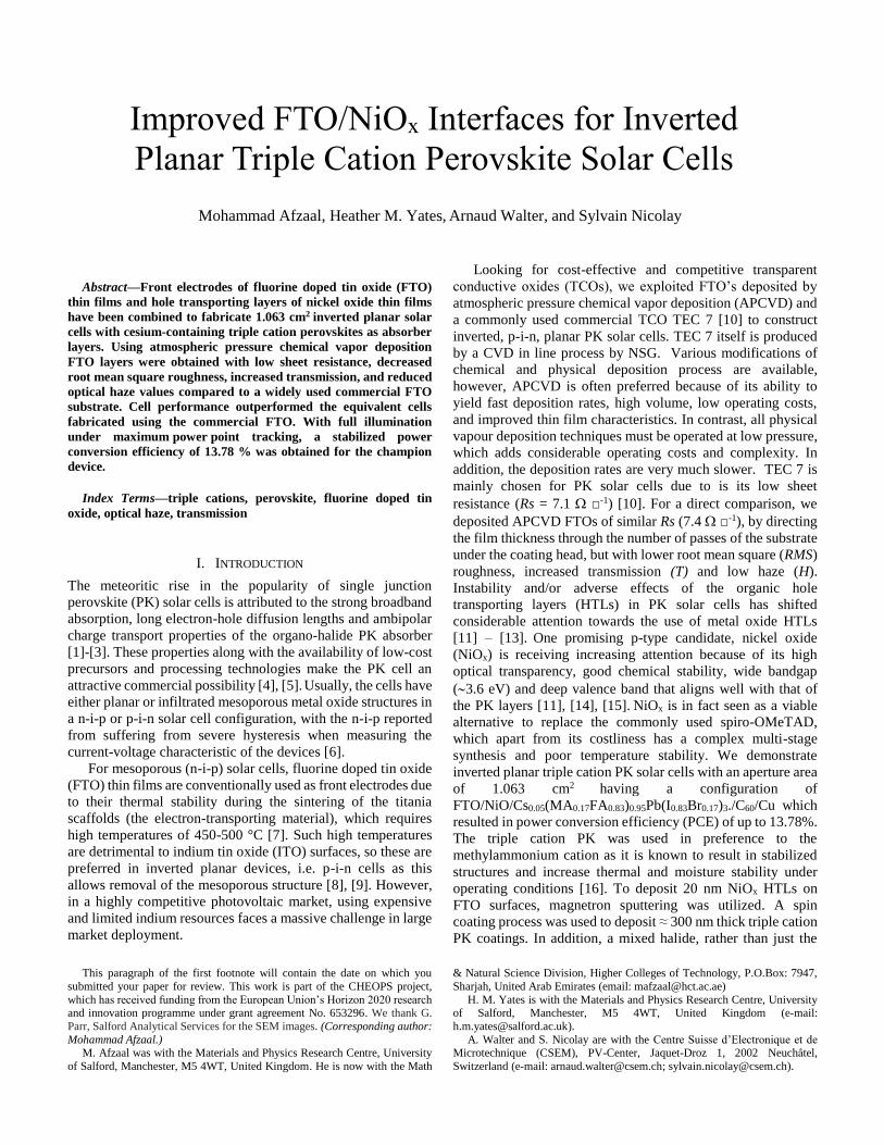
Deposition directly on glass established polycrystalline cubic
NiO (JCPDS-47-1049) with diffraction signals at 37.0o (111)
and 43.3o (200). The signal is relatively weak due to the thinness
of the film (20 nm). There was no obvious change in
crystallinity when sputtered onto FTO with the NiO (200) peak
and (111) as a shoulder on the FTO (200) peak (Fig.4).
The AFM (not given here) and SEM established the very
smooth nature of the NiOx when deposited directly on glass
with a mean roughness of approximately 1 nm. When deposited
on the FTO the surfaces looked very similar to the original FTO
surfaces, with only marginally lower roughness values,
suggesting the NiOx was deposited conformally. The RMS
values for TEC 7
Fig. 4. XRD patterns for sputtered NiO on glass and FTOs.
dropped from 35 nm to 32 nm on NiOx coating and that of the
APCVD FTO showed no change (18 nm).
The presence of the Ni and O was determined by EDAX.
The SEM and AFM for the NiOx/APCVD sample came from a
masked FTO sample so only selected areas of the film were
coated with NiOx. The images and EDAX were taken at both
positions where NiOx had been deposited and in between. The
lack of morphology changes on addition of the NiOx confirmed
the conformal nature of the coating.
Fig. 5. SEM images of a) NiO on glass, b) NiOx/APCVD FTO,
c) masked area on NiO/FTO film (i.e. no NiOx), d) NiOx/TEC7,
e) TEC7 and f) EDAX of two areas on patterned APCVD
FTO/NiOx sample.
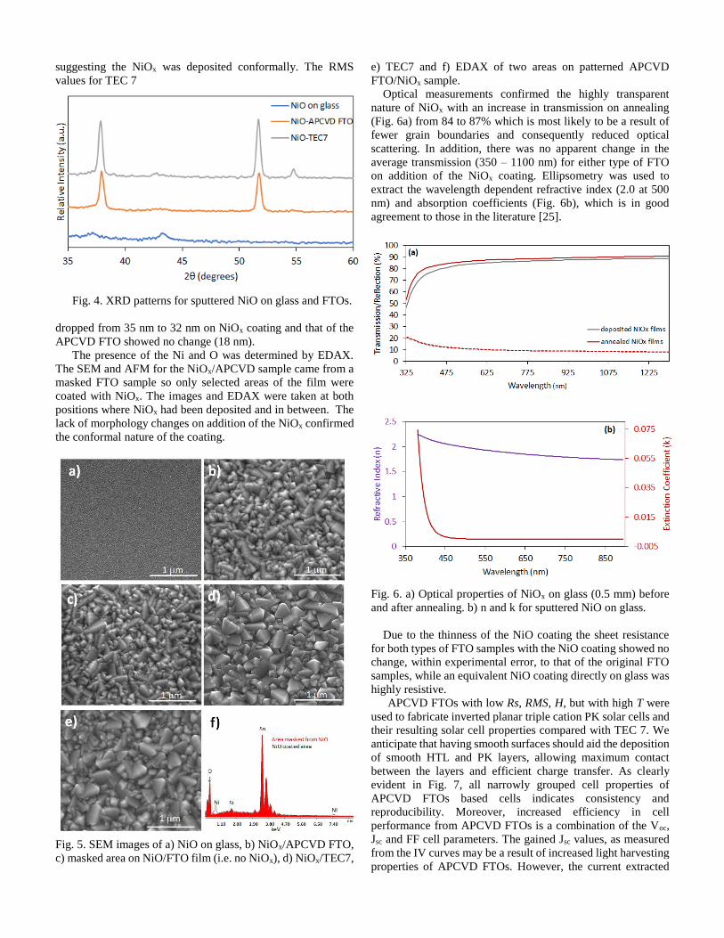
Optical measurements confirmed the highly transparent
nature of NiOx with an increase in transmission on annealing
(Fig. 6a) from 84 to 87% which is most likely to be a result of
fewer grain boundaries and consequently reduced optical
scattering. In addition, there was no apparent change in the
average transmission (350 – 1100 nm) for either type of FTO
on addition of the NiOx coating. Ellipsometry was used to
extract the wavelength dependent refractive index (2.0 at 500
nm) and absorption coefficients (Fig. 6b), which is in good
agreement to those in the literature [25].
Fig. 6. a) Optical properties of NiOx on glass (0.5 mm) before
and after annealing. b) n and k for sputtered NiO on glass.
Due to the thinness of the NiO coating the sheet resistance
for both types of FTO samples with the NiO coating showed no
change, within experimental error, to that of the original FTO
samples, while an equivalent NiO coating directly on glass was
highly resistive.
APCVD FTOs with low Rs, RMS, H, but with high T were
used to fabricate inverted planar triple cation PK solar cells and
their resulting solar cell properties compared with TEC 7. We
anticipate that having smooth surfaces should aid the deposition
of smooth HTL and PK layers, allowing maximum contact
between the layers and efficient charge transfer. As clearly
evident in Fig. 7, all narrowly grouped cell properties of
APCVD FTOs based cells indicates consistency and
reproducibility. Moreover, increased efficiency in cell
performance from APCVD FTOs is a combination of the Voc,
Jsc and FF cell parameters. The gained Jsc values, as measured
from the IV curves may be a result of increased light harvesting
properties of APCVD FTOs. However, the current extracted

from the External Quantum Efficiency (EQE) showed a much
smaller improvement with an average of 20.29 mA/cm2 ( =
0.15 mA/cm2) and 19.72 mA/cm2 ( = 0.35 mA/cm2) for the
APCVD FTO and TEC 7 based cells, respectively. This
suggests that there are other facts having a greater impact such
as improved charge collection due to maximized contact
between the layers on the smoother FTO. However, a plateau
of over 80 % EQE (410 nm to 740 nm) suggests high photon-
to-electron conversion in the cells (Fig. 8a). Improved FF and
reduced series resistance is usually related to reduced pinholes
(low recombination processes) and increased charge collection,
respectively. This again aided by the smoother surface of the
APCVD FTO, which may lead to better interface integrity with
subsequent layers and hence improved quality of the perovskite
deposition and so a reduction in cell shunts. Similarly, the mean
Vl value for APCVD FTO is significantly higher than that of the
TEC 7 derived cells. Current-voltage scans of champion
APCVD FTO based device demonstrated PCE of 13.78 % (Fig.
8b). From the external quantum efficiency curve, derived
current density of 20.3 mA cm-2 is consistent with the measured
value under simulated light.
Fig. 7. Statistical box plots of the inverted planar triple cation
PK solar cells (note: set 11 FTO labelled on x axis denotes
APCVD FTO).
Due to the wide variation in p-i-n device composition within the
scientific literature, it is very difficult to make direct
comparisons between results. Additionally, as previously
mentioned, the size of the reported cell can make a large
difference in PCE due to the increased likelihood of inclusion
of pinholes and/or defects within the area studied [26]. These in
turn leading to low resistance shunting paths and a reduction in
light absorption. The majority of work on inverted planar cell
structures is based on ITO substrates to achieve smooth
interfaces. For example, Lai et al. reported a PCE of 7.75 % for
ITO/NiOx/CH3NH3PbI3/PCBM/BCP/Al cell structures which
involved additional high-temperature annealing at 450 °C [27].
More recently, Weber et al. reported a PCE of 12.8% for a small
scale (0.09 cm2) p-i-n device with a cell configuration of
ITO/NiOx/PK/PC60BM/Ag using a
Cs0.08(MA0.17FA0.83)0.92Pb(I0.83Br0.17)3 based PK [28]. This
device, although closer to our device material structure is based
on an ITO rather than FTO TCO. Other recent work using FTO
along with a NiO HTL includes Tang et al [29] who achieved a
PCE of 11.82% when using similar thickness NiO to that used
by us, with an optimum of 15.47% for a much thicker HTL,
albeit with a much smaller cell size of 0.12 cm2. The authors
also emphasized the variation in PCE that is achieved by other
researchers dependent on the size, shape, and crystallinity of the
NiO. Zhu et al [30] reported PCE of 18.8% for a
FTO/NiO/MAPbI3/C60/SnO2/Ag configuration, is again not
directly comparable due to differences in perovskite
composition and use of nanocrystallite SnO2 as the ETL. The
effect on cell performance of differing NiOx, perovskite and
PCBM thicknesses is clearly reported by Yin et al [30] showing
a wide range in PCE highly dependent on the various film
thicknesses. Both Zhu [30] and Yin [31] reported high PCE’s
for their optimum FTO/NiO based devices, again not directly
comparable due to very different film thicknesses, use of only
the methylammonium cation and of greater importance the very
small sizes of the cells at 0.06 cm2 and 0.112 cm2.
Fig. 8: (a) EQE (b) current-voltage measurements for
champion perovskite solar cell.

In addition, the use of NiOx to enable the formation of a
planar p-i-n rather than n-i-p solar cell configuration showed a
reduction in hysteresis between the forward and reverse
current-voltage characteristics. A comparison between results
for planar MALI on our CVD FTO (with TiO2-x ETL) to the
present cells showed a factor of 10 reduction in hysteresis as
determined from the areas under the forward and reverse IV
curves. Hysteresis has been ascribed to the perovskite
crystallinity, degree of interface contact [32], excess mobile
ionic species and interfacial charge traps [33]. Previous
research suggested that perovskite quality is strongly influenced
by the underlying substrate [34] so possibly deposition on NiOx
rather than a TiO2-x surface, along with changes to the chemical
structure may have improved the crystallinity and interface
contact leading to a reduction in interfacial charge traps.
Although, a much bigger factor on the cell parameters is the
change from the use of NiOx as the HTL to TiO2-x as an ETL.
IV. CONCLUSION
We have successfully demonstrated that APCVD
deposited FTO front electrodes in conjunction with
sputtered NiOx HTL could be effectively used to construct
competitive large area inverted planar triple cation PK
solar cells. Unlike commonly used FTO surfaces, smooth
FTOs not only aids with improved physical contact
between the layers, but also reduces light scattering effects
at the surface. The outcome is evident in the form of
improved FF/lower series resistance pointing towards
reduced pinhole/reduced alternative recombinations.
REFERENCES
[1] M. M. Lee, J. Teuscher, T. Miyasaka, T. N. Murakami, and H. J.
Snaith, “Efficient Hybrid Solar Cells Based on Meso-Superstructured Organometal Halide Perovskites” Science, vol. 338, pp. 643-647, 2012,
doi: 10.1126/science.1228604.
[2] M. Liu, M. B. Johnston, and H. J. Snaith, “Efficient Planar Heterojunction Perovskite Solar Cells by Vapour Deposition” Nature,
vol. 501, pp. 395-398, 2013, doi: 10.1038/nature12509.
[3] N. J. Jeon, J. H. Noh, Y. C. Kim, W. S. Yang, S. Ryu, and S. I. Seok, “Compositional Engineering of Perovskite Materials for High-
Performance Solar Cells” Nature, vol. 517, pp. 476-480, 2015, doi:
10.1038/nature14133. [4] G. Xing, N. Mathews, S. Sun, S. S. Lim, Y. M. Lam, M. Grätzel, S.
Mhaisalkar, and T. C. Sum, “Long-range Balanced Electron-and Hole-
Transport Lengths in Organic-Inorganic CH3NH3PbI3” Science, vol. 342, pp. 344-347, 2013, doi: 10.1126/science.1243167.
[5] Q. Dong, Y. Fang, Y. Shao. P. Mulligan, J. Qiu, L. Cao, and J. Huang,
“Electron-Hole Diffusion Lengths > 175 μm in Solution-Grown
CH3NH3PbI3 Single Crystals” Science, vol. 347, pp. 967-970, 2015, doi:
10.1126/science.aaa5760.
[6] (a) J. H. Heo, H. J. Han, D. Kim, T. K. Ahn, and S. H. Im, “Hysteresis-less Inverted CH3NH3PbI3 Planar Perovskite Hybrid Solar Cells with 18.1%
Power Conversion Efficiency” Energy Environ. Sci. vol. 8 pp. 1602-1608,
2015, doi: 10.1039/C5EE00120J. (b) J. Seo, S. Park, Y. C. Kim, N. J. Jeon, J. H. Noh, S. C. Yoon, and S. I. Seok, “Benefits of Very Thin PCBM and
LiFL for Solution-Processed p–i–n Perovskite Solar Cells” Energy Environ.
Sci. vol. 7, pp. 2642-2646, 2014, doi: 10.1039/C4EE01216J. (c) N. J. Jeon, J. H. Noh, Y. C. Kim, W. S. Yang, S. Ryu, and S. I. Seok, “Solvent
Engineering for High-Performance Inorganic–Organic Hybrid
Perovskite Solar Cells” Nature Mater. vol. 13, pp. 897-903, 2014, doi: 10.1038/nmat4014.
[7] W. S. Yang, J. H. Noh, N. J. Jeon, Y. C. Kim, S. Ryu, J. Seo, and S. I. Seok, “High-Performance Photovoltaic Perovskite Layers Fabricated
through Intramolecular Exchange” Science, vol. 348, pp. 1234−1237.
2015, doi: 10.1126/science.aaa9272.
[8] P. S. C. Schulze, A. J. Bett, K. Winkler, A. Hinsch, S. Lee, S.
Mastroianni, L. E. Mundt, M. Mundus, U. Wurfel, S. W. Glunz, M.
Hermle, and J. C. Goldschmidt, “Novel Low-Temperature Process for Perovskite Solar Cells with a Mesoporous TiO2 Scaffold” ACS Appl.
Mater. Interfaces vol. 9, pp. 30567−30574, 2017, doi:
10.1021/acsami.7b05718. [9] https://www.ossila.com/products/ito-glass-substrate
[10] http://www.mtixtl.com/FTO-252522TEC7-25.aspx
[11] M. B. Islam, M. Yanagida, Y. Shirai, Y. Nabetani and K. Miyano, “NiOx Hole Transport Layer for Perovskite Solar Cells with Improved
Stability and Reproducibility” ACS Omega vol. 2, pp. 2291-2299, 2017,
doi: 10.1021/acsomega.7b00538. [12] J. H. Park, J. Seo, S. Park, S. S. Shin, Y. C. Kim, N. J. Jeon, H. W. Shin,
T. K. Ahn, J. H. Noh, S. C. Yoon, C. S. Hwang, and S. I. Seok, “Efficient
CH3NH3PbI3 Perovskite Solar Cells Employing Nanostructured p-Type NiO Electrode Formed by a Pulsed Laser Deposition” Adv. Mater. Vol.
27, pp. 4013−4019, 2015, doi: 10.1002/adma.201500523.
[13] A. B. Huang, J. T. Zhu, J. Y. Zheng, Y. Yu, Y.Liu, S. W. Yang, S. H.
Bao, L. Lei and P. Jin, “Achieving high-performance planar perovskite
solar cells with co-sputtered Co-doping NiOx hole transport layers by
efficient extraction and enhanced mobility” J. Mater. Chem. C vol. 4, pp. 10839-10846, 2016, doi: 10.1039/C6TC03624D.
[14] A. Liu, G. Liu, H. Zhu, B. Shin, E. Fortunato, R. Martins and F. Shan,
“Hole Mobility Modulation of Solution-Processed Nickel Oxide Thin-
Film Transistor Based on High-K Dielectric” Appl. Phys. Lett. Vol. 108, pp. 233506, doi: 10.1063/1.4953460.
[15] C. Park, J. Kim, K. Lee, S. K. Oh, H. J. Kang and N. S. Park, “Electronic,
Optical and Electrical Properties of Nickel Oxide Thin Films Grown by RF Magnetron Sputtering” Appl. Sci. Converg. Technol. Vol. 24, pp. 72-
76, 2015, do: 10.5757/ASCT.2015.24.3.72.
[16] M. Saliba, T. Matsui, J.-Y. Seo, K. Domanski, J.-P. Correa-Baena M. K. Nazeeruddin, W. Tress, A. Abate, A. Hagfeldtd and M. Grätzel,
“Cesium-containing triple cation perovskite solar cells: improved
stability, reproducibility and high efficiency” Energy Environ. Sci. vol. 9, pp. 1989-1997, 2016, doi: 10.1039/C5EE03874J.
[17] A. Sahu, and A. Dixit, “Inverted structure perovskite solar cells: A
theoretical study” Curr. Appl. Phys. vol. 18, pp. 1583-1591, 2018, doi: 10.1016/j.cap.2018.10.008.
[18] W. Chen, Y. Wu, Y. Yue, J. Liu, J. W. Zhang, X. Yang, H. Chen, E. Bi,
I. Ashraful, M. Grätzel, and L. Han, “Efficient and Stable Large-Area Perovskite Solar Cells With Inorganic Charge Extraction Layers” Science
vol. 350. pp. 944-948, 2015, doi: 10.1126/science.aad1015.
[19] M. Soliman, M. M. Hussein, S. El-Atway and M. E. El-Gamal, “Effect of Doping and Spraying Technique on the Properties of Tin Oxide Films”
Renewable Energy vol. 23, pp. 463–470, 2001, doi: 10.1016/S0960-
1481(00)00151-8. [20] C. Agashe, M. Takwale, V. Bhide, S. Mahamuni, S. K. Kulkarni, “Effect
of Sn Incorporation on the Growth Mechanism of Sprayer SnO2 Films”
J. Appl. Phys. vol. 70, pp. 7382–7386, 1991, doi: 10.1016/0167-577X(91)90135-S.
[21] A. Smith, J.-M. Laurent, D. S. Smith, J.-P. Bonnet and R. Clemente,
“Relation Between Solution Chemistry and morphology of SnO2-based Thin Films Deposited by a Pyrosol Process” Thin Solid Films vol. 266,
pp. 20-30, 1995, doi: 10.1016/0040-6090(95)06648-9.
[22] J. T. Wang, X. L. Shi, X. H. Zhong, J. N. Wang, L. Pyrah, K. D.
Sanderson, P. M. Ramsey, M. Hirata and K. Tsuri, “Morphology Control
of Fluorine-Doped Tin Oxide Thin Films For Enhanced Light Trapping”
Sol. Energy Mater. Sol. Cells vol. 132, pp. 578-588, 2015, doi: 10.1016/j.solmat.2014.09.043.
[23] H. M. Yates, P. Evans, D. W. Sheel, S. Nicolay, L. Ding, and C. Ballif,
“High-Performance Tandem Silicon Solar Cells on F:SnO2” Surf. Coat. Technol. Vol. 230, pp. 228–233, 2013, doi:
10.1016/j.surfcoat.2013.05.029.
[24] A. Mills, N. Elliott, I. P. Parkin, S. A. O’Neill and R. J. Clark, “Novel TiO2 CVD Films for Semiconductor Photocatalysis” J. Photochem.
PhotoBiol. A vol. 151, pp. 171-179, 2002, doi: 10.1016/S1010-
6030(02)00190-9. [25] B. Sasi K. G. Gopchandran, P. K. Manoj, P. Koshy, P. P. Rao and V. K.
Vaidyan, “Preparation of Transparent and Semiconducting NiO Films”

Vacuum. Vol. 68, pp. 149–154, 2003, doi: https://doi.org/10.1016/S0042-207X(02)00299-3.
[26] J. Werner, C. H. Weng, A. Walter, L. Fesquet, J. P. Seif, S. De Wolf, B.
Niesen and C. Ballif, “Efficient Monolithic Perovskite/Silicon Tandem
Solar Cell with Cell Area >1 cm2” J. Phys. Chem. Lett. Vol. 7, pp. 161-
166, 2016, doi: 10.1021/acs.jpclett.5b02686.
[27] W.-C. Lai, K.-W. Lin, T.-F. Guo and J. Lee, “Perovskite-based solar cells with nickel-oxidized nickel oxide hole transfer layer” IEEE Trans.
Electron Dev. vol. 62, pp. 1590–1595, 2015, doi:
10.1109/TED.2015.2413671. [28] S. Weber, T. Rath, J. Mangalam, B. Kunert, A. M. Coclite, M. Bauch, T.
Dimopoulos, and G. Trimmel, “Investigation of NiOx-hole transport
layers in triple cation perovskite solar cells” J. Mater. Sci. Mater. Electron vol. 29, pp. 1847-1855, 2018, doi: 10.1007/s10854-017-8094-
9.
[29] S. Tang, D. Jiao L. Zhang, X. Zhang, C. Xu, C. Yao, J. Wu, Z. Lan, “High-performance inverted planar perovskite solar cells based on
efficient hole-transporting layers from well-crystalline NiO
nanocrystals” Solar Energy, vol. 161, pp.100-108, 2018, doi: 10.1016/j.solener.2017.12.045.
[30] Z. Zhu, Y. Bai, X. Liu, C. C. Chueh, S. Yang and A. K. Jen, “Enhanced
efficiency and stability of inverted perovskite solar cells using highly
crystalline SnO2 nanocrystals as the robust electron transporting layer”
Adv. Mater. vol. 28, pp. 6478-6484, 2016, doi:
10.1002/adma.201600619. [31] X. Yin, Z. Yao, Q. Luo, X. Dai, Y. Zhou, Y. Zhang, Y. Zhou, S. Luo, J.
Li, N. Wang and H. Lin, “High efficiency inverted planar perovskite solar cells with solution-processed NiOx hole contact” ACS Appl. Mater. Interf.
vol. 9, pp. 2439−2448, 2017, doi: 10.1021/acsami.6b13372.
[32] E. L. Unger, E. T. Hoke, C. D. Bailie, W. H. Nguyen, A. R. Bowring, T. Heumüller, M. G. Christoforo and M. D. McGehee, “Hysteresis and
transient behavior in current-voltage measurements of hybrid perovskite
absorber solar cells” Energy Environ. Sci. vol. 7, pp. 3690-3698, 2014, doi: 10.1039/C4EE02465F.
[33] Y. Zhang, M. Liu, G. E. Eperon, C. T. Leijtens, D. McMeekin, M. Saliba,
W. Zhang, M. de Bastiani, A. Petrozza, L. M. Herz, M. B. Johnston, H. Lin, H. J. Snaith, “Charge selective contacts, mobile ions and anomalous
hysteresis in organo-inorganic perovskite solar cells” Mater. Horiz. vol.
2, pp. 315-322, 2015, doi: 10.1039/C4MH00238E. [34] J. You, L. Meng, T. B. Song, T. F. Guo, Y. M. Yang, W. H. Chang, Z.
Hong, H. Chen, H. Zhou, Q. Chen, Y. Liu, N. De Marco, and Y. Yang,
“Improved air stability of perovskite solar cells via solution processed metal oxide transport layers” Nat. Nanotechnol. vol. 11, pp. 75-81, 2016,
doi: 10.1038/nnano.2015.230.


![lbuf] ljsf;sf nIox¿ - UN Nepal Information Platform](https://img.dokumen.tips/doc/110x75/6291631db7b57c39db6663d3/lbuf-ljsfsf-niox-un-nepal-information-platform.jpg)


