Embed Size (px)
Citation preview

Institutionen för systemteknikDepartment of Electrical Engineering
Examensarbete
Implementation of LTE baseband algorithms for a
highly parallel DSP platform
Examensarbete utfört i Datorteknikvid Tekniska högskolan vid Linköpings universitet
av
Markus Keller
LiTH-ISY-EX--16/4941--SE
Linköping 2016
Department of Electrical Engineering Linköpings tekniska högskolaLinköpings universitet Linköpings universitetSE-581 83 Linköping, Sweden 581 83 Linköping


Implementation of LTE baseband algorithms for ahighly parallel DSP platform
Examensarbete utfört i Datorteknik
vid Tekniska högskolan i Linköpingav
Markus Keller
LiTH-ISY-EX--16/4941--SE
Handledare: Dake Liuisy, Linköpings universitet
Di Wuisy, Linköpings universitet
Examinator: Andreas Ehliarisy, Linköpings universitet
Linköping, 25 April, 2016


Avdelning, Institution
Division, Department
Division of Computer EngineeringDepartment of Electrical EngineeringLinköpings universitetSE-581 83 Linköping, Sweden
Datum
Date
2016-04-25
Språk
Language
� Svenska/Swedish
� Engelska/English
�
⊠
Rapporttyp
Report category
� Licentiatavhandling
� Examensarbete
� C-uppsats
� D-uppsats
� Övrig rapport
�
⊠
URL för elektronisk version
http://www.da.isy.liu.se
http://www.ep.liu.se
ISBN
—
ISRN
LiTH-ISY-EX--16/4941--SE
Serietitel och serienummer
Title of series, numberingISSN
—
Titel
TitleGenomförandet av LTE basband algoritmer för en parallell DSP plattform
Implementation of LTE baseband algorithms for a highly parallel DSP platform
Författare
AuthorMarkus Keller
Sammanfattning
Abstract
The division of computer engineering at Linköping’s university is currentlydeveloping an innovative parallel DSP processor architecture called ePUMA. Onepossible future purpose of the ePUMA that has been thought of is to implement itin base stations for mobile communication. In order to investigate the performanceand potential of the ePUMA as a processing unit in base stations, a model of theLTE physical layer uplink receiving chain has been simulated in Matlab and thenpartially mapped onto the ePUMA processor.
The project work included research and understanding of the LTE standard andsimulating the uplink processing chain in Matlab for a transmission bandwidth of5 MHz. Major tasks of the DSP implementation included the development of a300-point FFT algorithm and a channel equalization algorithm for the SIMD unitsof the ePUMA platform. This thesis provides the reader with an introduction tothe LTE standard as well as an introduction to the ePUMA processor. Further-more, it can serve as a guidance to develop mixed point radix FFTs in general orthe 300 point FFT in specific and can help with a basic understanding of channelequalization. The work of the thesis included the whole developing chain from un-derstanding the algorithms, simplifying and mapping them onto a DSP platform,and testing and verification of the results.
Nyckelord
Keywords SIMD, DSP, FFT, DFT, LTE, OFDM, ePUMA, sleipnir, Cooley Tukey, Zero-forcing, Channel equalization


Abstract
The division of computer engineering at Linköping’s university is currentlydeveloping an innovative parallel DSP processor architecture called ePUMA. Onepossible future purpose of the ePUMA that has been thought of is to implement itin base stations for mobile communication. In order to investigate the performanceand potential of the ePUMA as a processing unit in base stations, a model of theLTE physical layer uplink receiving chain has been simulated in Matlab and thenpartially mapped onto the ePUMA processor.
The project work included research and understanding of the LTE standardand simulating the uplink processing chain in Matlab for a transmission bandwidthof 5 MHz. Major tasks of the DSP implementation included the development of a300-point FFT algorithm and a channel equalization algorithm for the SIMD unitsof the ePUMA platform. This thesis provides the reader with an introduction tothe LTE standard as well as an introduction to the ePUMA processor. Further-more, it can serve as a guidance to develop mixed point radix FFTs in general orthe 300 point FFT in specific and can help with a basic understanding of channelequalization. The work of the thesis included the whole developing chain from un-derstanding the algorithms, simplifying and mapping them onto a DSP platform,and testing and verification of the results.
v


Acknowledgments
First of all, I would like to thank both professor Dake Liu for the opportunity towork with this interesting thesis topic as well as my examiner Andreas Ehliar forhis valuable input regarding my thesis report. Also I would like to thank AndreasKarlsson for his helpful support with any questions I had regarding programmingthe sleipnir processor and Di Wu for his support with LTE related questions.
Another thanks goes to my opponent Mohamed Lababidi for his commentsregarding my thesis, which helped me to improve the quality of the report.
Last but not least I would like to thank my parents for giving me the oppor-tunity to study abroad and for their love, support and patience.
vii


Contents
1 Introduction 31.1 Background . . . . . . . . . . . . . . . . . . . . . . . . . . . . . . . 31.2 Scope . . . . . . . . . . . . . . . . . . . . . . . . . . . . . . . . . . 31.3 Outline . . . . . . . . . . . . . . . . . . . . . . . . . . . . . . . . . 4
2 LTE, Long Term Evolution 72.1 Background . . . . . . . . . . . . . . . . . . . . . . . . . . . . . . . 72.2 Design targets . . . . . . . . . . . . . . . . . . . . . . . . . . . . . . 8
2.2.1 Capabilities . . . . . . . . . . . . . . . . . . . . . . . . . . . 82.2.2 System performance . . . . . . . . . . . . . . . . . . . . . . 82.2.3 Deployment-related aspects . . . . . . . . . . . . . . . . . . 92.2.4 Strategies to meet the design targets . . . . . . . . . . . . . 9
2.3 OFDM . . . . . . . . . . . . . . . . . . . . . . . . . . . . . . . . . . 102.3.1 Multi-carrier transmission . . . . . . . . . . . . . . . . . . . 102.3.2 Physical Resource . . . . . . . . . . . . . . . . . . . . . . . 112.3.3 Orthogonality . . . . . . . . . . . . . . . . . . . . . . . . . . 122.3.4 Cyclic prefix . . . . . . . . . . . . . . . . . . . . . . . . . . 132.3.5 Modulation using FFT processing . . . . . . . . . . . . . . 132.3.6 Advantages and drawbacks . . . . . . . . . . . . . . . . . . 16
2.4 SC-FDMA . . . . . . . . . . . . . . . . . . . . . . . . . . . . . . . . 172.4.1 DFT-spread OFDM processing chain . . . . . . . . . . . . . 17
2.5 Frame structure . . . . . . . . . . . . . . . . . . . . . . . . . . . . . 182.6 Reference signals . . . . . . . . . . . . . . . . . . . . . . . . . . . . 20
2.6.1 Downlink reference signals . . . . . . . . . . . . . . . . . . . 212.6.2 Uplink reference signals . . . . . . . . . . . . . . . . . . . . 22
3 Project implementation 253.1 Project overview . . . . . . . . . . . . . . . . . . . . . . . . . . . . 25
3.1.1 General assumptions . . . . . . . . . . . . . . . . . . . . . . 253.1.2 Transmission bandwidths . . . . . . . . . . . . . . . . . . . 263.1.3 The uplink receiving processing chain . . . . . . . . . . . . 26
3.2 Channel estimation and signal equalization . . . . . . . . . . . . . 273.2.1 Channel estimation . . . . . . . . . . . . . . . . . . . . . . . 283.2.2 Channel equalization with Zero forcing . . . . . . . . . . . . 29
ix
x Contents
3.3 Implementation in Matlab . . . . . . . . . . . . . . . . . . . . . . . 29
4 The ePuma DSP platform 334.1 Background . . . . . . . . . . . . . . . . . . . . . . . . . . . . . . . 334.2 The ePUMA architecture . . . . . . . . . . . . . . . . . . . . . . . 344.3 Memory subsystem and data communication . . . . . . . . . . . . 35
4.3.1 Memory hierarchy . . . . . . . . . . . . . . . . . . . . . . . 364.3.2 Data communication . . . . . . . . . . . . . . . . . . . . . . 37
4.4 The ePUMA Master . . . . . . . . . . . . . . . . . . . . . . . . . . 384.5 The SIMD processors . . . . . . . . . . . . . . . . . . . . . . . . . 39
4.5.1 Supported datatypes . . . . . . . . . . . . . . . . . . . . . . 394.5.2 Sleipnir datapath . . . . . . . . . . . . . . . . . . . . . . . . 404.5.3 Memory components and registers . . . . . . . . . . . . . . 414.5.4 Data access of LVMs and vector register file . . . . . . . . . 414.5.5 Programming the sleipnir . . . . . . . . . . . . . . . . . . . 43
5 FFT implementation 515.1 DFT and IDFT relation . . . . . . . . . . . . . . . . . . . . . . . . 515.2 Fast Fourier Transformation . . . . . . . . . . . . . . . . . . . . . . 53
5.2.1 Cooley-Tukey FFT algorithm . . . . . . . . . . . . . . . . . 535.2.2 Radix-4 and Radix-2 FFTs . . . . . . . . . . . . . . . . . . 58
5.3 300 point FFT Implementation for Sleipnir . . . . . . . . . . . . . 585.3.1 Cycle cost estimations . . . . . . . . . . . . . . . . . . . . . 595.3.2 Assembly implementation . . . . . . . . . . . . . . . . . . . 615.3.3 Cycle costs . . . . . . . . . . . . . . . . . . . . . . . . . . . 63
6 Implementing the channel equalization 656.1 Implementing the computation of the channel estimate . . . . . . . 656.2 Implementing the zero-forcing equalizer . . . . . . . . . . . . . . . 66
6.2.1 Kernel for 1/x . . . . . . . . . . . . . . . . . . . . . . . . . 686.2.2 Assembly code and cycle cost . . . . . . . . . . . . . . . . . 68
6.3 Cycle cost . . . . . . . . . . . . . . . . . . . . . . . . . . . . . . . . 71
7 Results and discussion 737.1 Cycle cost of FFT algorithm . . . . . . . . . . . . . . . . . . . . . 737.2 Evaluation of the results . . . . . . . . . . . . . . . . . . . . . . . . 747.3 Challenges of the implementation . . . . . . . . . . . . . . . . . . . 76
8 Conclusions 798.1 Future work . . . . . . . . . . . . . . . . . . . . . . . . . . . . . . . 80
Bibliography 83
A Kernel for 300 point FFT 85

List of abbreviations
3G Third generation3GPP Third generation partnership projectALU Arithmetic logic unitBS Base stationBW BandwidthCM Constant memoryCP Cyclic prefixCPU Central processing unitD/A Digital to analogDAC Digital to analog converterDL DownlinkDFT Discrete fourier transformDMA Direct memory accessDFTS-OFDM DFT spread OFDMDSP Digital signal processor/processingePUMA Embedded parallel DSP processor with Unique Memory AccessFDD Frequency divsion duplexFFT Fast fourier transformHSPA High speed packet accessIDFT Inverse discrete fourier transformIFFT Inverse fast fourier transformISY Institutionen för systemteknikLTE Long term evolutionLVM Local vector memoryMBMS Multimedia broadcast multicast serviceMIMO Multiple input multiple outputMMSE Minimum Mean Square ErrorPM Program memoryPPU Packet processing unitOFDM Orthogonal frequency-division multiplexingQAM Quadrature amplitude modulation
1

2 Contents
QPSK Quadrature phase-shift keyingRB Resource blockRF Radio frequencyRISC Reduced instruction set computingSC-FDMA Single carrier frequency division multiple accessSIMD Single instruction multiple datapathTDD Time divison duplexUL UplinkVRF Vector register fileWCDMA Wideband code division multiple access

Chapter 1
Introduction
1.1 Background
Recent trends in the development of computer technology show an increasingimportance of parallel computing methods to fulfill the ever rising demands oncomputational performance. With this development trend in line, the division ofcomputer engineering at Linköping’s university is currently developing a highlyparallel DSP platform called ePUMA. The platform consists of a master-processorand eight SIMD co-processors called sleipnir, which are capable of 128-bit vec-tor operations. By combining the multi-core processor design approach with theSIMD approach, an embedded DSP platform capable of high performance parallelcomputing shall be created.
The ePUMA is considered to be used in various DSP fields like, for example,baseband signal and radar signal processing, video games and video coding anddecoding [12]. This thesis will investigate the ePUMA’s potential of serving as aprocessing unit in base stations supporting LTE, the latest developed standard formobile communication. For this purpose, a model of the LTE uplink communica-tion has been developed and parts of the processing chain have been mapped ontothe ePUMA.
1.2 Scope
In order to achieve the goal of implementing LTE-baseband algorithms for theePUMA, the software Matlab has been used as a tool for implementing a sim-plified model of the complete LTE physical layer processing chain at the uplinkreceiver side. The communication was modeled for a transmission bandwidth of5 MHz, for which the LTE baseband processing includes the computation of a300 point IFFT computation. For the ePUMA platform, the main focus was toimplement certain algorithms which were included in this processing chain for theSIMD sleipnir co-processors. The implementations that have been made for theco-processors are a 300-point FFT computation and a channel equalization algo-
3

4 Introduction
rithm. This thesis provides the theoretical background for understanding the LTEbaseband processing that has been modeled in Matlab and for understanding thealgorithm implementations that have been made for the ePUMA. Since the imple-mentation of the baseband uplink receiving chain is a challenging task, a highlysimplified model of the uplink LTE baseband receiver has been used as a basis forthe implementations made in this thesis.
1.3 Outline
The thesis is organized into the following chapters:
• Chapter 2 - LTE Introduction gives an introduction to the LTE stan-dard. The chapter begins with a discussion of the driving forces mostrelevant for the market of mobile communications and explains to whichLTE design targets these driving forces have led. Based on that, thereader can get a deeper understanding of the motivations for using cer-tain technologies in the LTE standard. The chapter mainly focuses onaspects that help understanding the LTE physical layer processing andthe baseband algorithms that were implemented in this thesis. In par-ticular it will be clarified why the LTE baseband processing includesFFT computations and how the LTE standard defines reference sym-bols that can be used for channel equalization.
• Chapter 3 - Project Implementation presents an overview of the projectand the scope of the implementations that have been made in Matlaband for the ePUMA. With the basic knowledge about the LTE standarddiscussed in the previous chapter, we will have a basis to understandthe model of the physical layer LTE uplink chain that has been imple-mented. This chapter discusses which assumptions and simplificationshave been made to derive the Matlab model of the LTE uplink base-band processing at the receiver side. Furthermore, it will be clarifiedwhich parts of the uplink processing chain have been mapped onto theePUMA.
• Chapter 4 - The ePUMA platform gives an introduction to the ePUMADSP platform. This chapter discusses why the concept of the ePUMAplatform of utilizing different forms of computing parallelism is coherentwith recent trends in processor technologies. Furthermore, it providesthe reader with an overview of the architecture of the platform. Themain focus of the chapter however, is to explain how the eight SIMDprocessors of the ePUMA are programmable in order to enable thereader to understand the implementations that have been made in thisthesis.
• Chapter 5 - Implementing 300 point FFT provides a detailed descrip-tion of how the 300 point FFT has been implemented for the SIMD

1.3 Outline 5
processors of the ePUMA. The chapter begins with presenting the the-oretical background that is the base for deriving the FFT algorithmwhich has been used. Furthermore, it will be shown which minimumcycle cost is theoretically achievable with the approach used for thealgorithm implementation in this work.
• Chapter 6 - Implementing the channel equalization This chapter de-scribes how the channel equalization has been implemented for theSIMD processors of the ePUMA, and which cycle cost the executionof the algorithm requires.
• Chapter 7 - Results and discussion Presents the results of the thesis.The chapter discusses the cycle cost that has been achieved and thechallenges that have been faced during the implementation. Based onthat, some potential improvements for the SIMD co-processors are sug-gested.
• Chapter 8 - Conclusion The last chapter concludes the thesis with a sum-mary of the work, a final discussion about ePUMA’s potential as aprocessing unit in base stations, and suggestions for future work.


Chapter 2
LTE, Long Term Evolution
2.1 Background
The demands on mobile communication systems are continuously growing, dueto the rapidly increasing numbers of mobile users worldwide and a hard compe-tition between various existing and new network operators and vendors [4]. Thiscompetition leads to a constant development of new standards and technologiesin order to provide new services for the mobile users as well as existing services inbetter ways and at a lower cost [4]. More and more people are interested in broad-band data access everywhere in order to use services like email-synchronization,internet access, file download, video streaming, teleconferencing and other specificapplications for their mobile devices [10],[14].
Due to the challenge of increasing numbers of mobile users on the one handand their requests for more advanced services on the other hand, the requirementson advanced mobile systems of today are very widely spread and include highdemands on service data rates, user throughput, mobility, cell coverage, spectrumefficiency, spectrum flexibility, system complexity and many more [3]. There-fore, developing mobile systems has become a very complex and challenging task,which is being carried out by global standard-developing organizations such as theThird Generation Partnership Project (3GPP) including thousands of people [4].With over 3 billion users, the mobile system technologies specified by 3GPP arethe most widely distributed in the world and the partners of the project includeorganizations from China, Europe, Japan, Korea and the USA [4]. Long TermEvolution (LTE) is the latest standard for mobile communication systems devel-oped by 3GPP and was first launched for commercial use in December 2009 inStockholm and Oslo. The number of users have been continuously growing sinceand in 2015 LTE has been launched in 93 countries while the total number of LTEsubscription was reported to have reached the 500 million mark.
7

8 LTE, Long Term Evolution
2.2 Design targets
In the following some important design targets of LTE will be explained. Weshould note here, that all of those design targets have even been surpassed bythe current performance of LTE. The LTE requirements can be divided into sevendifferent categories [4]:
• Capabilities: Uplink and downlink data-rates
• System performance: User throughput, spectrum efficiency, mobility andcoverage
• Deployment related aspects: Spectrum flexibility, spectrum deployment,and coexistence with other 3GPP standards
• Architecture and migration: LTE Radio Access Network architecture de-sign targets
• Radio resource management: Specification for support of higher-layertransmission and for load sharing and authority management betweendifferent radio access technologies
• Complexity: Overall system-complexity as well as complexity of the mobileterminal
• General aspects: Cost and service related aspects
We will discuss the first three categories in more detail, as it will help tounderstand the motivation for implementing certain technologies in LTE, whichare relevant for the algorithms implemented in this thesis.
2.2.1 Capabilities
The LTE standard offers peak data rates which are around ten times higher thanprevious third generation (3G) standards. For the downlink (DL) transmission,that means from the base stations (BS) to the mobile user, data rates up to100 Mbit/s can be achieved in the maximum supported transmission bandwidthof 20 MHz[3]. The uplink (UL) communication (from mobile user to BS) offersdata rates up to 50 Mbit/s for this bandwidth [3]. Decreasing the transmissionbandwidth will proportionally decrease the peak data rate and thus we can expressthe LTE data rate requirements as 5 bit/s/Hz for the DL and 2.5 bit/s/Hz for theUL [4].
2.2.2 System performance
The system performance specifications define the targets for user throughput, spec-trum efficiency, mobility, coverage and Multimedia Broadcast or Multicast Services(MBMS). In the LTE specifications these design targets are defined in comparisonto an earlier 3GPP standard namely Release 6 HSPA [4].

2.2 Design targets 9
User throughput describes how many mobile users can be served simultaneouslyby the LTE system in a certain cell, or in other words, in the coverage area ofa certain base station. Compared to the earlier HSPA standard, the averageuser throughput is aimed to be 3 to 4 times higher for DL and 2 to 3 timeshigher for UL.[4]
Spectrum efficiency describes the system throughput within one cell per band-width and is thus measured in bit/s/MHz/cell. Similar to the average userthroughput, the LTE spectrum efficiency shall be improved around 3 to 4times for DL and 2 to 3 times for UL. [4]
Mobility requirements address the mobile terminals’ speed. According to thedesign targets, maximum performance can be achieved for low mobile ter-minal speeds between 0-15 km/h and for speeds up to 120 km/h LTE isstill able to provide a relatively high performance. The maximum speed ofa mobile terminal that can be handled by LTE depends on the frequencybands and lies within 350 to 500 km/h [4].
Coverage requirements deal with the cell radius, which defines the maximumpossible distance between a base station and the mobile terminal connectedto the base station. The requirements for the user throughput, spectrumefficiency and mobility mentioned above shall be achieved for a cell radiusup to 5 km, while a slight decrease in performance is tolerated for a cellrange up to 30 km [4].
MBMS requirements deal with the so called point to multipoint services thatallow sending the same data to many mobile users simultaneously. PossibleMBMS services could include for example mobile TV or radio broadcastingand shall have a higher performance than in previous standards. The designtarget for the spectral efficiency of MBMS services is defined as 1 bit/s/Hz[4].
2.2.3 Deployment-related aspects
The deployment-related aspects deal mainly with the frequencies used by the LTEsystem. Since it should be possible to install LTE step by step in frequency bandswhich are already allocated by other 2G or 3G standards, the requirements onthe spectrum flexibility of LTE are very high. The specifications define that LTEshould support both TDD and FDD which makes it possible that LTE can beused both in paired and unpaired spectrum allocations [10]. Furthermore LTEshould be usable in different frequency bands and support scalable transmissionbandwidths. The standard includes 6 different transmission bandwidths whichrange from 1.4 MHZ up to 20 MHz[10].
2.2.4 Strategies to meet the design targets
We can summarize here that some of the main design targets of LTE are a highsystem performance in terms of data rate, spectrum efficiency and user through-put on the one hand, as well as high spectrum flexibility in order to make LTE

10 LTE, Long Term Evolution
compatible with other already existing mobile systems on the other hand. Thetechnical innovations included in LTE are enormous and it is beyond the scope ofthis thesis to discuss all of them in detail. Instead we will focus on some aspectsof the LTE standard, which are important to meet the ambitious design targets,and which will help us to understand the uplink processing algorithms developedfor the ePUMA processor in this thesis work.
Two of the key technologies for LTE to achieve the design targets mentionedabove are multi antenna techniques and Orthogonal Frequency Division Multi-plexing (OFDM)[10]. Multi antenna techniques have already been widely usedin former mobile standards. The usage of more than one antenna at transmitterand/or receiver side can significantly increase the system performance in respectto user throughput, coverage, and data rates. Despite of the importance of multiantenna techniques for the LTE standard, they are somewhat out of the scope ofthis thesis. In the following section we will describe OFDM, which is another veryimportant technique of LTE and more relevant for the algorithms implemented inthis thesis.
2.3 OFDM
OFDM has been adopted for LTE downlink communication after it had previouslysuccessfully been used for several other technologies including for example digitalaudio and video broadcasting for local area networks [17]. It offers several bene-fits for achieving the LTE design targets including a high spectral efficiency androbustness against frequency selective fading caused by multipath propagation [3].
2.3.1 Multi-carrier transmission
OFDM is a special form of a multi-carrier transmission scheme. In a multi-carriertransmission the data that shall be transmitted is divided into several smaller datastreams, which are then being transmitted in parallel and on different frequencybands as illustrated in Figure 2.1 [3]. These signals with a smaller bandwidth areoften called subcarriers.
���������
�������
�� �����
�
����������������
����������������
����������������
����������������
�����������
�����������
�����������
�����������
�� �
Figure 2.1. Dividing data stream on multiple carriers
The input Xk represents a data stream of complex modulated symbols from

2.3 OFDM 11
any complex alphabet like for example QPSK. Depending on the chanel quality thetransmission is either performed with modulation schemes corresponding to higherdata rates (such as 64QAM), or with modulation schemes offering lower data rates(such as QPSK)[2]. Since the data streams are transmitted over different carrierfrequencies they can be restored at the receiver side by the use of correlators[3]. Figure 2.2 [3] illustrates the corresponding spectrum of the multicarriertransmission with four subcarriers, considered in our example.
One of the main differences between OFDM and other multi-carrier transmis-sion schemes used in previous standards like for example in Wideband Code Divi-sion Multiple Access (WCDMA) is that OFDM uses a significantly higher numberof subcarriers which allocate relatively small frequency bands. A transmissionbandwidth of 20 MHz for example would be equivalent to four subcarriers withapproximately 5Mhz bandwidth each in WCDMA, but in LTE the same overalltransmission bandwidth consists of 1200 subcarriers [4]. Another difference be-
Figure 2.2. Spectrum multi-carrier transmission
tween OFDM and ordinary multi carrier transmission is that in the later one thespectra of the different subcarriers should not overlap (compare 2.2), in order toprevent them from interfering and distorting each other. Therefore multi-carriertransmission schemes usually do not offer a very high spectral efficiency as thesubcarriers cannot be packed very closely together [4]. However OFDM, despite ofbeing a multicarrier transmission scheme, offers a relatively high spectral efficiency[3]. This is achieved by introducing orthogonal subcarriers which will be explainedin more detail later.
2.3.2 Physical Resource
Since in OFDM transmission the data stream gets transmitted over such a rela-tively large number of different carrier frequencies in parallel, it is common practiceto illustrate the physical resource of the transmitted signal in both time and fre-quency domain, as shown in Figure 2.3.
In the horizontal axis, representing the time domain, we can see the OFDMsymbols, each of which are transmitted during a time-duration Ts. In the verticalaxis we can see the frequency band, containing the NC subcarriers of the OFDMsignal. It is important to understand here that this picture only illustrates howthe OFDM signal can be interpreted while it is transmitted over the radio channelbut not how the LTE signal looks like during baseband processing. After the

12 LTE, Long Term Evolution
Figure 2.3. OFDM time frequency grid
receiver has executed steps like down-conversion, sampling and parallel to serialconversion, obviously this signal illustration is no longer valid. We will explain thecomplete transmission chain later in this chapter.
Figure 2.4 [3] illustrates a possible implementation for modulating an OFDMsignal. This image shows what happens during one symbol duration time Ts.
2.3.3 Orthogonality
As mentioned before, multi carrier transmission schemes do not generally offera high spectral efficiency due to the required guard bands between neighboringsubcarriers. OFDM solves this problem by creating subcarriers which have gotoverlapping spectra and are pairwise orthogonal to each other. Due to their or-thogonality, the subcarriers can be transmitted over carrier-frequencies which arevery close to each other in frequency domain, but still do not interfere with eachother. The orthogonality of the subcarriers is achieved by a rectangular pulseshaping and by choosing a suitable subcarrier spacing of ∆f = 1/Ts [4], whereTs stands for the symbol duration time. The rectangular pulse shaping leads toa sinc-shaped spectrum for each subcarrier. In Figure 2.5 it can be seen how thesinc-shaped spectra of five OFDM subcarriers overlap with each other. A proof ofthe pairwise orthogonality of the LTE subcarriers can be found in [4].
In LTE the subcarrier spacing ∆f is specified as 15 kHz [17]. Depending onthe total transmission BW, this means that the total number of subcarriers Nc

2.3 OFDM 13
Figure 2.4. OFDM modulation
lays in the range between 75 and 1200.
2.3.4 Cyclic prefix
As mentioned previously, the subcarriers are pairwise orthogonal to each other dueto the specific subcarrier spacing on the one hand and the sinc shaped spectrum ofthe subcarriers on the other hand. However, a time-dispersive radio channel canchange the spectrum shape of a transmitted signal. If such a change in spectrumshape befalls the subcarriers of an OFDM signal, they will to some extent losetheir pairwise orthogonality and since the spectra of the different subcarriers fun-damentally overlap with each other, it is a reasonable assumption that this mayresult in strong interferences between the subcarriers. Another problem is that aninter-symbol interference might occur within single subcarriers due to multipathpropagation. In order to make the OFDM signal robust against the corruptioncaused by time dispersive channels and multipath propagation, a so called cyclicprefix is added to the OFDM symbols in time domain. [3] This means that thelast part of the OFDM symbol is copied and added again in front of the OFDMsymbol.
2.3.5 Modulation using FFT processing
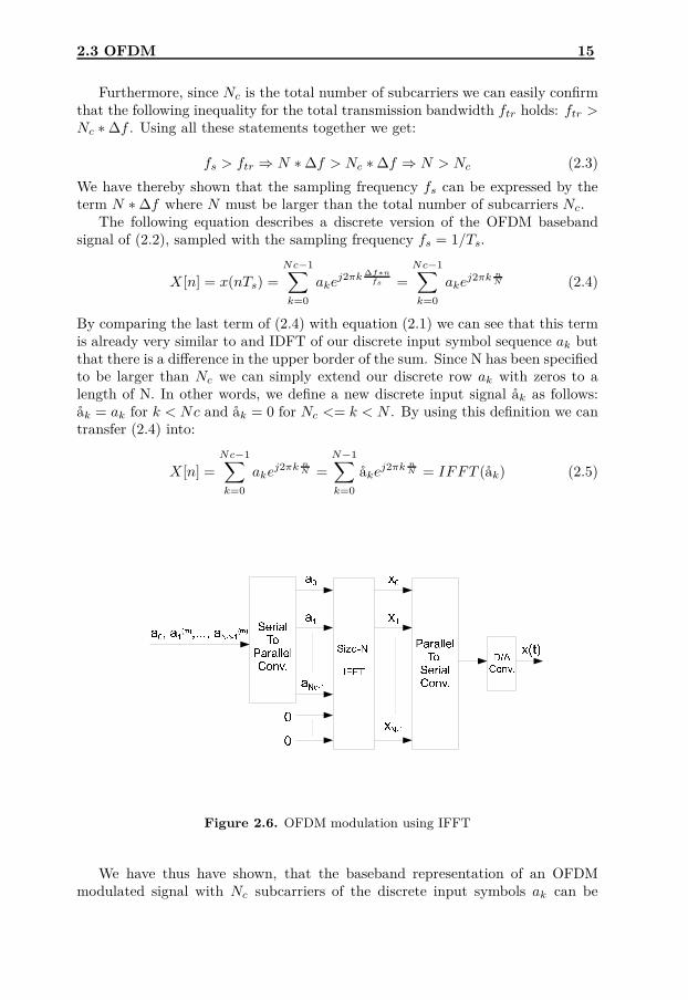
While Figure 2.4 illustrates the theoretical principle of creating an OFDM mod-ulated signal, there is in common practice a faster method being used for OFDMmodulation which includes FFT processing. In order to understand how FFT andIFFT processing can be used for OFDM modulation, we first recall that the for-mula for an inverse Discrete Fourier Transform X of a sampled signal x of length

14 LTE, Long Term Evolution
−4 −3 −2 −1 0 1 2 3 4−0.4
−0.2
0
0.2
0.4
0.6
0.8
1
1.2
Normalized frequency in ∆f=1/TS
Mag
nitu
de
∆ f = 1/TS
Figure 2.5. OFDM subcarrier spectra
N is defined as [18]:
X [n] =N−1∑
k=0
xkej2πnk/N (2.1)
Let us now have another look at Figure 2.4 and recall that the differencebetween any two neighboring subcarrier-frequencies is always constant and definedas ∆f . We can then conclude that it is possible to express an OFDM signal inbaseband notation as:
X(t) =
Nc−1∑
k=0
akej2πk∆ft (2.2)
When we talk about baseband notation here, we assume the OFDM signal hasbeen down-converted, or not yet up-converted. In other words, if we modulatean OFDM signal by means of IFFT processing, we do not need several mixers forup-converting every single carrier frequency, but instead we can just up-convertthe whole sum of subcarrier signals to a center frequency in the middle of thefrequency band allocated by the carrier frequencies. Before up-conversion or afterdown-conversion the OFDM signal can be described as in (2.2).
In the following, we will consider a time-discrete version X [n] of the signal,which can be obtained by sampling X(t) with a sampling rate of fs. We recallthat in order to be able to fully reconstruct a time continuos signal from its time-discrete sampled form, the sampling theorem has to be fulfilled, which defines howhigh the sampling frequency fs has to be in comparism to the highest frequencycomponent included in the signal. For the LTE standard it has been specified,that the sampling frequency fs should be a multiple of the subcarrier spacing ∆fand should be sufficiently higher than the transmission bandwidth ftr [3]. We canthen express the sampling frequency as fs = N ∗ ∆f .
2.3 OFDM 15
Furthermore, since Nc is the total number of subcarriers we can easily confirmthat the following inequality for the total transmission bandwidth ftr holds: ftr >Nc ∗ ∆f . Using all these statements together we get:
fs > ftr ⇒ N ∗ ∆f > Nc ∗ ∆f ⇒ N > Nc (2.3)
We have thereby shown that the sampling frequency fs can be expressed by theterm N ∗ ∆f where N must be larger than the total number of subcarriers Nc.
The following equation describes a discrete version of the OFDM basebandsignal of (2.2), sampled with the sampling frequency fs = 1/Ts.
X [n] = x(nTs) =
Nc−1∑
k=0
akej2πk ∆f∗n
fs =
Nc−1∑
k=0
akej2πk nN (2.4)
By comparing the last term of (2.4) with equation (2.1) we can see that this termis already very similar to and IDFT of our discrete input symbol sequence ak butthat there is a difference in the upper border of the sum. Since N has been specifiedto be larger than Nc we can simply extend our discrete row ak with zeros to alength of N. In other words, we define a new discrete input signal åk as follows:åk = ak for k < Nc and åk = 0 for Nc <= k < N . By using this definition we cantransfer (2.4) into:
X [n] =
Nc−1∑
k=0
akej2πk nN =
N−1∑
k=0
åkej2πk nN = IFFT (åk) (2.5)
Figure 2.6. OFDM modulation using IFFT
We have thus have shown, that the baseband representation of an OFDMmodulated signal with Nc subcarriers of the discrete input symbols ak can be

16 LTE, Long Term Evolution
created by means of IFFT processing. Figure 2.6 [4] shows a schematic drawing ofhow the modulation is achieved. The demodulation can be achieved accordinglyby using FFT processing as illustrated in Figure 2.7 [4].
Figure 2.7. OFDM de-modulation using FFT
We should note here that OFDM modulation and de-modulation by usingFFTs and IFFTs are very attractive implementation methods due to their lowcomputational cost [3].
2.3.6 Advantages and drawbacks
We can conclude that some of the main advantages of OFDM include its high spec-tral efficiency and a good robustness against frequency selective fading, due to therelatively narrow bandwidths of the subcarriers. Furthermore, it allows for highlyefficient modulation methods by use of FFT/IFFT processing and for a straight-forward realization of flexible transmission bandwidths, simply by adjusting thenumber of subcarriers which are allocated by the user of interest. Note that thisflexibility was defined as one of the main LTE design targets in the specifications.
There are other advantages of OFDM that are beneficial from a mobile systemperspective point of view. It offers for example a very good support for multi-broadcast transmission, which are transmissions that are sent simultaneously toall users in the system like for instance, mobile television [3]. Cell edge users whotypically have a relatively poor performance can experience significant benefits formulti-broadcast reception in an OFDM system, because the received signals fromdifferent surrounding cells can be combined in their mobile [3]. The combination ofsignals from different cells usually introduces time dispersion due to the differentdistances between user and BS. However, in the case of OFDM, the cyclic prefixescan compensate for a big part of this time dispersion which may significantly

2.4 SC-FDMA 17
increase the signal quality [3]. There are more mobile system benefits of OFDMlike its suitability as a user-multiplexing and multiple-access scheme which we willnot discuss in detail since they are beyond the scope of this thesis.
One of the main drawbacks of OFDM is that it typically introduces largevariations in the instantaneous transmission power [3]. This simply results fromthe fact that it is a multi carrier transmission scheme. We can understand thisin a somewhat simplified way, if we just assume that introducing a larger numberof subcarriers, will naturally cause the total transmission power to vary strongerover time. The problem with rapid and relatively strong changes in transmissionpower is, that they typically can produce nonlinearities in the transmitter whichdistort the signal [4]. In order to avoid or mitigate this issue, it is necessary toover-dimension the transmitter. But that consequently decreases the transmitter’sefficiency and increases power consumption. Thus OFDM is more suitable for theDL than for the UL, since in mobile terminals the power efficiency is much morecrucial than in the base stations [4].
2.4 SC-FDMA
SC-FDMA (Single carrier frequency division multiple access) has been chosen asthe transmission scheme for the LTE uplink. It is very similar to OFDM butthe instantaneous transmission power variations are reduced by execution of anadditional FFT processing step. For this reason SC-FDMA is also referred to asDFT-spread OFDM [4].
2.4.1 DFT-spread OFDM processing chain
One simple way to interprete the SC-FDMA transmission scheme is to see it asa conventional OFDM transmission, combined with a DFT based pre-coding [3].Figure 2.8 shows some of the processing steps to be executed for SC-FDMA trans-mission. The receiver part of this chain has been implemented in Matlab and forthe ePUMA. We should note here that some processing steps are missing in thisfigure such as, for instance, the channel equalization part. A more complete chainwill be presented in chapter 3. However, we can observe that this processing chainlooks very similar to conventional OFDM transmission except for one additionalFFT processing step, namely an extra smaller length FFT processing block in thetransmitter part and, anologously, one extra IFFT block in the receiver part. Thisextra FFT processing reduces the instantaneous power variations which makesSC-FDMA more suitable for uplink communication than OFDM [17]. Despite ofthis difference, SC-FDMA has got a lot of similarities with OFDM. So can, forexample, the SC-FDMA physical resource as well be seen as a time-frequency gridwith a subcarrier spacing of ∆f = 15 kHz [10]. A difference is here though that,in case of SC-FDMA, the resources allocated to certain mobile users must consistof a set of consecutive subcarriers. The reason for this is that otherwise the single-carrier property of the uplink transmission would be lost. User multiplexing hasnot been considered in this thesis and thus this issue will not be explained anyfurther here. For more details the reader is referred to [3] or [10].
18 LTE, Long Term Evolution
Figure 2.8. DFT-spread OFDM transmitter and receiver
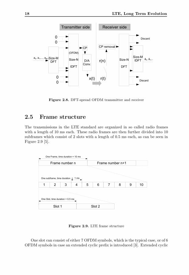
2.5 Frame structure
The transmissions in the LTE standard are organized in so called radio frameswith a length of 10 ms each. These radio frames are then further divided into 10subframes which consist of 2 slots with a length of 0.5 ms each, as can be seen inFigure 2.9 [5].
Figure 2.9. LTE frame structure
One slot can consist of either 7 OFDM symbols, which is the typical case, or of 6OFDM symbols in case an extended cyclic prefix is introduced [3]. Extended cyclic

2.5 Frame structure 19
prefixes are typically used if it is necessary to compensate for a high delay-spreadintroduced by the channel, or in case of multicast or broadcast transmissions [3],where the different time delays from different base stations to the user need to becompensated for. Figure 2.10 illustrates the time lengths of the cyclic prefixes inboth normal and extended versions.
Figure 2.10. Slot structure
In this picture, Tu represents the useful symbol time, and Tcp and Tcp−e standfor the normal and extended cyclic prefix time durations. In case a normal cyclicprefix length is used, the length of the first of the 7 OFDM symbols is with a totaltime duration of 5.1 µs a bit longer than the other six prefixes [3]. The reasonfor this is simply that all time durations in LTE are defined as multiple of a baseunit Ts and one slot with a time duration of 0.5 ms has got a number of 15360of these time intervalls Ts [3]. Since this number cannot be divided by seven, thefirst cyclic prefix has been specified to be slightly longer than the others.
The time frequency grid in LTE is furthermore divided into so called resourceblocks and schedule blocks. One resource block consists of 12 subcarriers in thefrequency domain and of one slot in the time domain. A schedule block consistsof two resource blocks and thus has got the time duration of one subframe. As thename implies, a schedule block is the smallest unit of the physical resource gridthat can be scheduled for a certain user. The reason for also defining the smallerresource blocks is, that LTE supports a so called frequency hopping transmissionmode for which the transmission frequency of the user of interest changes on a slotbasis [3].
In Figure 2.11 it is illustrated how the schedule and resource blocks are definedin the time frequency grid. The image shows four schedule blocks which are spreadover two slots and a total bandwidth of 360 kHz. One resource block consists ofup to 12 * 7 = 84 resource elements in total, which are the smallest physical units

20 LTE, Long Term Evolution
Figure 2.11. Scheduleblocks
of the time frequency grid. One resource element carries the information of onecomplex modulated symbol.
One reason for organizing LTE in a radio frame structure including slots andsubframes is related to LTE control signals as will be explained in the followig. Theradio signals, that are transmitted in the LTE standard, do not carry only the datawhich is is of direct interest for the user, but they also contain many different typesof control data, which ensures a sufficient service quality for the user. This controldata includes for example signals for estimating and communicating the channelquality between users and base station in order to choose suitable modulation andcoding schemes and to adapt the transmission power. Some of these control signalsin LTE need to be transmitted more often than others and therefore certain controlsignals could for example allocate specific resources in just every radio frame andothers in every single subframe.
In the next section we are going to discuss one specific control signal calleddemodulation reference signal which has been used for channel equalization in thebaseband processing chain implemented in this thesis work.
2.6 Reference signals
Since radio channels vary over time and over different frequencies, it is necessaryto estimate how the channel affects and corrupts the transmitted signal, in order

2.6 Reference signals 21
to successfully demodulate and recover the transmitted data at the receiver. Wediscussed earlier that in OFDM each subcarrier has got a relatively narrow band-width in frequency domain. Therefore, we can assume the corresponding channelof each subcarrier can be assumed to be non frequency selective, which meansthat its transfer function will not vary over different frequencies in this frequencyband [14]. In the case of OFDM it is therefore not necessary to define a continuoschannel transfer function H(f) over the whole transmission bandwidth at a certainpoint in time. We can instead describe the channel conditions in a discrete form bydefining a complex value Hk for each of the n subcarriers. These complex valueswill naturally vary over time, as the channels of the subcarriers vary over time. Inorder to equalize the received signal, an estimate of these complex values is neededat the receiver side. A convenient solution for retrieving these channel estimatesis to insert so called demodulation reference symbols, which are known at the re-ceiver side, into the time frequency grid. The channel estimates Hk can then becalculated simply by dividing the received symbols yk by the known transmittedreference symbols xk: Hk = yk/xk. In LTE there are differences between thedefinitions of these reference signals for the up and downlink, as will be describedin the following.
2.6.1 Downlink reference signals
The reference symbols in LTE are inserted into every single resource block in or-der to take the channel variations in time and frequency domains into account.In Figure 2.12 we can see an example of how the reference symbols are typicallyspread inside one schedule block for a downlink transmission [4]. The image il-lustrates only one out of six possible frequency shifts which are specified for thereference symbols [4]. Since we have got 12 subcarriers in total of which only twoare allocated for the reference symbols, there are five more possibilities how thereference symbols can be divided in a schedule block. One benefit of this is thatneighboring cells can use different frequency shifts for the reference signals, whichreduces the interference of reference signals between cells [4].
Obviously the resource elements reserved for reference symbols cannot be usedfor user data transmission. The decision about how many reference symbols shouldbe inserted into the time-frequency grid thus represents a tradeoff between priori-tising data throughput or accuracy of the channel estimates. We should notehere that it is furthermore possible in certain scenarios to improve the quality ofthe channel estimates, by averaging them over a certain number in time domainand/or in frequency domain. Wether such an averaging is beneficial, depends onthe channel conditions more specifically its coherence time and coherence band-width. The coherence time of a channel is the maximum time period during whichthis channel can be assumed to be time invariant while coherence bandwidth isthe maximum frequency band for which the channel can be considered to be nonfrequency selective [1]. Averaging over channel estimates of different time slots cantherefore be beneficial if the coherence time of the channel is not too small, meansthat the channel conditions are not varying too fast over time. Analogously aver-aging over channel estimates from different resource blocks in frequency domain

22 LTE, Long Term Evolution
Figure 2.12. Downlink reference signals
would typically give better results in case of a high channel coherence bandwidth.
2.6.2 Uplink reference signals
In the uplink the reference signals are not defined for specific resource elements,but instead they are defined in certain DFTS-OFDM symbols and allocate thecomplete transmission frequency band as illustrated in Figure 2.13 [4]. As we cansee, the reference signals are defined for every fourth OFDM symbol inside a slotso that every subframe contains two reference signal transmissions.
The main reason for defining complete DFTS-OFDM symbols as referencesignals, is the previously discussed uplink requirement for low power variationsduring transmissions [4]. In order to keep power variations low, it is not suit-able to frequency multiplex reference signal transmissions with other uplink datatransmissions like it is the case for the downlink [4].
A reference signal consists of a certain number of complex reference symbolswhich are known to the receiver. Since the uplink reference signal is transmittedover the complete transmission bandwidth, this implies that the number of complexsymbols of a reference signal sequence is equal to the total number of subcarriersincluded in this transmission bandwidth. Furthermore, since the transmissionbandwidths are always defined over certain numbers of resource blocks with 12subcarriers each, the number of complex symbols in a reference signal sequence

2.6 Reference signals 23
Figure 2.13. Uplink reference signals
will also be a multiple of 12 [4]. In general it is desirable for uplink referencesignals to have the following properties [4]:
• The power should not vary too strong in frequency domain, in order to ensurerelatively similar quality of channel estimation for different frequencies.
• The power variations in time domain should not be too strong either, sincestrong variations would decrease the power-amplifier efficiency.
• Neighboring cells should be able to use different reference signal sequencesfrom each other, in order to reduce inter cell interference. This implies that itshould be possible to define a sufficient number of different reference signals.
In order to achieve these targets in LTE, the uplink reference signals are de-fined to be extended versions of so-called Zadoff-Chu sequences, which have gotconstant power in both time and frequency domain and that makes them very suit-able as reference signals[4]. A Zadoff-Chu sequence is expressed by the followingequation[4]:
XZCk = e−jπu(k(k+1)/MZc ) · · · 0 <= k < MZc (2.6)
The variable MZc stands for the length of the Zadoff-Chu sequence. For aspecific length MZc, not only one single Zadoff-Chu sequence exists, but rather

24 LTE, Long Term Evolution
a set of different Zadoff-Chu sequences. This is indicated by the value u in theequation, which is an index value that defines a specific sequence of the set ofZadoff-Chu sequences with length MZc. The varialbe u can take all integer valueswhich are smaller than MZc and relatively prime to MZc. Thus, we can concludethat if we define the length MZc of a set to be a prime number, there will be moreZadoff-Chu sequences available, compared to choosing a non primary number in asimilar order of magnitude as length. Since it is desirable to be able to define asmany different reference signals as possible, Zadoff-Chu sequences with a prime-number length would be a very suitable choice as reference signals for LTE [3].However, this is not possible because the sequence must be a multiple of 12 as wediscussed earlier. Instead, the LTE standard defines the uplink reference signals tobe cyclic extensions of prime-number Zadoff-Chu sequences [3]. This simply meansthat from a given transmission bandwidth with a certain number of subcarriers n,the largest prime-number smaller than n is chosen as MZc [3]. Any of the Zadoff-Chu sequences of the set defined by MZc can then be transformed into a referencesignal sequence with length n, by adding to it n − MZc cyclic extensions of theSequence.
Figure 2.14 shows an example, created with matlab, of an LTE reference signalsequence of length n=300, defined by a Zadoff-Chu sequence of length MZc = 293.We can see in the figure the constant power of the complex symbols, as they forma circle.
The reference signal length of 300, which has been used here, is equivalentto a transmission bandwidth of 5 MHz, as will be explained in more detail in thefollowing chapter which describes the actual algorithms implemented in this thesis.
−1 −0.8 −0.6 −0.4 −0.2 0 0.2 0.4 0.6 0.8 1
−1
−0.8
−0.6
−0.4
−0.2
0
0.2
0.4
0.6
0.8
1
Qua
drat
ure
In−Phase
Scatter plot
Figure 2.14. Zadoff Chu reference sequence

Chapter 3
Project implementation
In the following, we will present a high level description of the LTE uplink al-gorithms that have been implemented for the ePUMA processor. This chapterwill provide the reader with an understanding of the project content and how theuplink chain was simulated in Matlab. The detailed ePUMA implementation willbe described in later chapters.
3.1 Project overview
The purpose of this project work was to evaluate the potential of the ePUMA as aprocessing unit inside an LTE base station, which implies that it was of interest toeither implement the downlink transmission part, or the uplink receiving part onthe ePUMA. For this thesis, it has been decided to focus on the uplink receivingpart. The complete chain for uplink baseband processing on the receiver side hasbeen implemented first in Matlab and parts of it have then been mapped onto theePUMA. However, since designing a complete functional LTE uplink receiver isa very challenging task, we had to make certain assumptions and simplificationsin order to reduce the complexity to a suitable level. We can therefore describethe thesis work as an implementation of a highly simplified model for the physicallayer processing of an LTE uplink receiver.
3.1.1 General assumptions
The following assumptions have been made for the transmitted signal which shouldbe processed at the receiver side in this project.
• Total transmission bandwidth of 5 MHz
• No MIMO activated
• Frequency hopping deactivated
• One user transmits over the complete bandwidth
25

26 Project implementation
• 64 QAM modulation
The specific bandwidth of 5 MHz has mainly been chosen because it corre-sponds to a 300 point IFFT processing, which was useful to implement for theePUMA because it would make implementation of other FFT sizes defined inLTE, a relatively easy task.
3.1.2 Transmission bandwidths
In line with the LTE design targets for a high spectrum flexibility, LTE supportsa total of six different transmission bandwidths [4]. Since different transmissionbandwidths correspond to different numbers of OFDM subcarriers, they also intro-duce different FFT lengths in the OFDM modulation and demodulation process-ing blocks. The following table shows the transmission bandwidths defined by theLTE specifications and their corresponding FFT/IFFT sizes. “Number of RB’s”describes how many resource blocks are included in the respective transmissionbandwidth and the total number of subcarriers within the bandwidth is definedby the value “M”. We should recall here that the M-FFT sizes are only relevantfor the uplink because they are a part of the SC-FDMA processing chain, but theyare not included in the case of OFDM transmissions.
Table 3.1. Transmission bandwidths and corresponding FFT/IFFT sizes
Transmission BW 1.4 MHz 3 MHz 5 MHz 10 MHz 15 MHz 20 MHz
Nr of RB’s 6 15 25 50 75 100M-FFT size 72 180 300 600 900 1200N-FFT size 128 256 512 1024 1536 2048
As we can see modulation/demodulation of an OFDM signal with a 5 MHztransmission bandwidth includes 512 point and 300 point FFT/IFFT processingsteps. While a 512 point FFT algorithm had already been implemented for theePUMA previous to this thesis work, implementing the 300 point FFT for theePUMA was one of the main workloads of the project.
3.1.3 The uplink receiving processing chain
In the following section we will present all the processing steps that had to be exe-cuted by the ePUMA. Figure 3.1 illustrates the computational operations includedin LTE UL layer 1 processing and highlights which of them were implemented forthe ePUMA platform.
We can see in the illustration that as a first step the subcarrier spacing needsto be removed, which can be achieved by multiplying the input sequence with asequence of appropriate phase shifts. This step is only necessary in the uplinkprocessing chain, not in the downlink. Then, after cyclic prefix removal and 512point FFT processing, the channel has to be estimated with help of the referencesignal included in the fourth DFTS-OFDM symbol in every slot. By using the

3.2 Channel estimation and signal equalization 27
inverse of the estimate, the six remaining OFDM symbols can then be equalized.In the project we used a simple straightforward solution called zero forcing asequalization method, which will be explained in more detail later. Finally, after300 point IFFT processing the complex symbols can be recovered and detected.
Figure 3.1. Uplink physical layer processing chain for 5MHz BW
It should be noted here, that the detection block has not been implemented inthe ePUMA. Since we did not assume channel estimation errors in our simplifiedmodel, the complex symbols could perfectly be recovered after channel equalizationwithout using a detector. Furthermore, rather than implementing a 300 pointIFFT, a 300 point FFT was implemented for the ePUMA because an IFFT canbe computed in a relatively simple way by using an FFT computation of equallength as will be shown in chapter 5. The illustrated processing chain has beenimplemented for the ePUMA from the subcarrier spacing removal step to thechannel equalization step. For the 300 point IFFT part we limited our workloadto merely developing a 300 point FFT kernel for the sleipnir and a theoreticalproof of how the IFFT can be computed from the FFT results in a simple way.
3.2 Channel estimation and signal equalization
In the algorithm implementation for the channel estimation, we did not use anyaveraging between consecutive channel estimates over time or frequency domain.Instead, 300 complex channel estimates have been calculated for each slot, usingthe 300 reference symbols which are known at the receiver side and which arelocated in the slot’s forth OFDM symbol. These channel estimates have then

28 Project implementation
been used for equalizing the six remaining DFTS-OFDM symbols in the slot,which contain the data to be transmitted.
3.2.1 Channel estimation
If we assume that the coherence time of our channel is shorter than 0.5 ms, wecan consider the channel to be time invariant for the time duration of one slot.It is therefore possible to model the channel for that time duration by a transferfunction H(f) which is only dependent on the frequency. In frequency domain wethen have the following relation between the signal X which is transmitted overthe channel and the received signal Y:
Y (f) = H(f) ∗ X(f) (3.1)
However, as we mentioned before the subcarriers have got a narrow transmission-band which can be considered to be non frequency selective. In other words if thebandwidth of the subcarriers is smaller than the correlation bandwidth of thechannel, the channel response will not vary over frequency within the band of onesubcarrier. This is illustrated in Figure 3.2.
Figure 3.2. Frequency selective channel transfer function
We can see that the channel response varies over different frequencies, but atthe same time the channel response inside a subcarrier band is relatively constant.Thus, the narrow bandwidths of the subcarriers allow us to model the channelresponse of one subcarrier to be independent of the frequency domain. If we recallfurthermore that each subcarrier carries exactly one complex symbol inside oneDFTS-OFDM symbol we can define a vector Xk containing all complex symbolsinside one DFTS-OFDM symbol, with 0 < k <= M .
M represents here the total number of subcarriers included in the transmissionbandwidth (300 in our case). From a baseband perspective, the channel transfer

3.3 Implementation in Matlab 29
function for each of the subcarriers can simply be represented by a complex valueHk which is multiplied with the complex symbol Xk, carried by the subcarrier. Ifwe then define the corresponding vector Yk, containing the received data symbols,we get the following representation:
Yk = Hk ∗ Xk (3.2)
The channel estimates Hk can therfore be calculated by:
Hk =Yk
Xk= Yk ∗
1
|Xk|∗ Xk (3.3)
3.2.2 Channel equalization with Zero forcing
The channel equalization has been realized by implementing a zero forcing al-gorithm. Zero forcing is a straightforward method for equalization, where thereceived signal gets multiplied with the inverse of the channel response. The namezero forcing has been chosen, because this algorithm reduces the intersymbol in-terference to zero in case of noise free scenarios [1]. The main disadvantage of thisequalization methods is, that filtering the received filter with the inverse channelresponse may amplify noise at specific frequencies where the channel spectrum hasgot a high attenuation [1]. For this reason zero forcing is typically not as oftenused for radio communication systems, as more robust methods like for exampleLeast-Mean Square Equalization. However, for low noise scenarios the method pe-forms well and can therefore be used for our simplified model in order to perfectlyrecover the data. The zero forcing equalization can be realized by implementingthe following equation:
Xk = Yk ∗ Hk−1
= Yk ∗1
ˆ|Hk|2 ∗
¯Hk (3.4)
The expression¯
Hk represents here the complex conjugate of the channel es-timates. The reader might wonder here why the last term in (3.4) represents asimplification compared to Xk = Yk ∗ 1
Hk
. As we will see in more detail later, for
the ePUMA, being a fixed point processing platform, division is not a trivial taskand it is therefore more convenient to implement a division with a real value, in
this case represented by ˆ|Hk|, instead of dividing by the complex value Hk.
3.3 Implementation in Matlab
The receiver part of the previously described uplink processing chain has beenimplemented both in Matlab and for the ePUMA. Another software has been usedto generate a digital DFTS-OFDM modulated LTE uplink signal with a transmis-sion bandwidth of 5 MHz and 64 QAM as modulation scheme. We implementedthen a simple channel model in Matlab in order to simulate the changes the LTEsignal experiences, when being transmitted over a radio channel. Throughout the

30 Project implementation
complete project work matlab has been used as a reference and assisting tool fordeveloping the different kernels or algorithms for the ePUMA.
Figure 3.3. The project realization
The Matlab code for the uplink processing steps can be seen in the code ex-ample 3.1.
Listing 3.1. Matlab code LTE uplink processing chain
1 %% Import LTE s i g n a l2 mydata= lte_fdd_UL_5MHz_64QAM_nofilter_basic ( 1 : end , 1 )3 +lte_fdd_UL_5MHz_64QAM_nofilter_basic ( 1 : end , 2 )∗ 1 i ;45 %% Create channel r e sponse6 hcoe f=randn (3 ,1)+ randn (3 ,1 )∗1 i ;7 h = [ hcoe f (1 )∗3 0 0 2∗ hcoe f (2 ) 0 hcoe f ( 3 ) ] ;8 h = h/norm(h ) ;9
10 % Create r e c e i v e d s i g n a l by convo lut ing transmitted11 % s i g n a l with channel r e sponse12 rx_s igna l=conv ( mydata . ’ , h ) . ’ ;13 rx_s igna l=rx_s igna l ( 1 : end −5);1415 % Cyc l i c p r e f i x removal16 sym(: ,1 )= rx_s igna l (41 : (41+511 ) ) ;17 o f f s e t =40+512;18 sym16=rx_s igna l ( o f f s e t +1:( o f f s e t +(512+36)∗6));19 sym16=reshape ( sym16 , 5 1 2 + 3 6 , [ ] ) ;2021 % Subca r r i e r spac ing removal22 sym ( : , 2 : 7 ) = sym16 ( 3 7 : end , : ) ;

3.3 Implementation in Matlab 31
23 ha l fcShi f tSym=sym . ∗ repmat ( exp(−1 i ∗ pi / 5 1 2 ∗ ( 1 : 5 1 2 ) . ’ ) , 1 , 7 ) ;2425 % 512 po int FFT p r o c e s s i n g step26 rx_sym_fft=1/ s q r t (512)/ s q r t (512/300)∗ f f t ( ha l fc_shi fted_sym ) ;27 rx_shi f=c i r c s h i f t ( rx_sym_fft , 1 5 0 ) ;2829 % Compute channel e s t imate s30 hest=re fe rence_s igna l_mul . ∗ r x_sh i f t ( 1 : 3 0 0 , 4 ) ;31 conj ( hes t )=c_h ;3233 % Channel e q u a l i z a t i o n34 rx_sh i f t (1 : 300 ,1 )=1 ./ ( hes t . ∗ c_h ) . ∗ c_h . ∗ r x_sh i f t ( 1 : 3 0 0 , 1 ) ;35 rx_sh i f t (1 : 300 ,2 )=1 ./ ( hes t . ∗ c_h ) . ∗ c_h . ∗ r x_sh i f t ( 1 : 3 0 0 , 2 ) ;36 rx_sh i f t (1 : 300 ,3 )=1 ./ ( hes t . ∗ c_h ) . ∗ c_h . ∗ r x_sh i f t ( 1 : 3 0 0 , 3 ) ;37 rx_sh i f t (1 : 300 ,5 )=1 ./ ( hes t . ∗ c_h ) . ∗ c_h . ∗ r x_sh i f t ( 1 : 3 0 0 , 5 ) ;38 rx_sh i f t (1 : 300 ,6 )=1 ./ ( hes t . ∗ c_h ) . ∗ c_h . ∗ r x_sh i f t ( 1 : 3 0 0 , 6 ) ;39 rx_sh i f t (1 : 300 ,7 )=1 ./ ( hes t . ∗ c_h ) . ∗ c_h . ∗ r x_sh i f t ( 1 : 3 0 0 , 7 ) ;4041 % 300 po int IFFT p r o c e s s i n g step42 rx_sym=s q r t (300)∗ i f f t ( r x_sh i f t ( 1 : 3 0 0 , : ) ) ;4344 s c a t t e r p l o t ( reshape ( rx_sym ( : , 1 : 3 ) , [ ] , 1 ) ) ;
Executing the code above will generate the following figure, in which we cansee the 64QAM constellation, which indicates, that the signal has succesfully beendemodulated.
−0.4 −0.2 0 0.2 0.4
−0.4
−0.3
−0.2
−0.1
0
0.1
0.2
0.3
0.4
Qua
drat
ure
In−Phase
Scatter plot
Figure 3.4. 64QAM constellation after signal demodulation


Chapter 4
The ePuma DSP platform
In the following chapter we will give an introduction to the ePUMA architectureand its processing components. The main scope of this chapter is to provide thereader with the necessary background for understanding the implementations thathave been made in this thesis, rather than including all details of the ePUMA ar-chitecture. For a more complete introduction to the ePUMA the reader is referredto [12] and [21].
4.1 Background
Recent trends in the development of computer technology show an increasing im-portance of parallel computing methods to fulfill the ever rising demands on com-putational performance. Parallel computing methods can be distinguished intothe following three different categories.
1. The development and programming of multi-core processors which is calledtask parallelism.
2. The usage of processors that operate on vectorized data which utilizes theso called data parallelism. An example for this kind of processors operatingon vectorized data are SIMD’s, which stands for “Single instruction multipledata” [15].
3. A third form of parallelism finally, that can be exploited by parallel comput-ing methods is the instruction level parallelism, where the general idea is toexecute different instructions simultaneously, if their results do not dependon each other. One technique that makes use of instruction level parallelismis the pipelining approach, where the execution times of consecutive instruc-tions partially overlap with each other.
Several reasons for the increased usage of parallel computing methods in gen-eral and the development towards multi-core processors in particular can be found.
33

34 The ePuma DSP platform
Many of them are related to the following three factors, which cause significant lim-itations for further performance improvements of traditional single core processors[13]:
• Performance improvements reached by using higher CPU clock frequencieshave basically come to an end mainly because this method causes unsatis-factory high levels of power consumption.
• The instruction level parallelism has already been exploited to large degreesand thus in general little further performance gains are to be expected fromthis method.
• Memory speeds so far cannot keep up with the ever increasing processorspeeds, whichs limits the overall performance improvements reached withhigher processor speeds.
The trend towards higher computing parallelism can be observed both for gen-eral purpose computers as well as for embedded systems which typically targetreal-time signal processing. The development of the highly parallel ePUMA DSPplatform is therefore coherent with the current developments in computing tech-nology.
The ePUMA is planned to be used in various DSP fields like for examplebaseband signal and radar signal processing, video games and video coding anddecoding [12]. The main design goal is to offer an embedded platform capable ofhigh performance parallel computing while simultaneously consuming little powerand having low silicon cost [21]. In order to achieve that purpose ePUMA has beendesigned in an innovative way that enables the platform to exploit different formsof computing parallelism. The design combines the multi-core approach with theSIMD approach and furthermore includes a unique memory subsystem which isaimed at hiding memory access time behind the computing time of the program[21],[12].
4.2 The ePUMA architecture
In the following we will give a brief overview of the ePUMA architecture. The plat-form contains a master RISC (Reduced Instruction Set Computing) DSP processorand eight SIMD co-processors together on a single chip [12]. This multi-core designincluding eight processors with vectorized data processing capabilities is the keyto epumas potential for high performance computations since it allows for strongutilization of task- and data-parallelism simultaneously. Signal processing tasks,that can be vectorized, can be divided onto up to eight SIMD processors, whichare all capable of high throughput for arithmetic calculations. The SIMD coresare therefore intended to be used as the main data processing units of the ePUMAplatform. The master DSP processor on the other hand, has got various tasksincluding:
• Control of the overall ePUMA program flow and execution which includesfor example the transmission of start commands to the SIMDs.

4.3 Memory subsystem and data communication 35
• Control of the data transfer between main memory and SIMDs by configu-ration and initialization of DMA transactions.
• Calculating parts of application algorithms which cannot be vectorized andtherefore not efficiently handled by the SIMD processors.
• Computation of smaller tasks for which transferring them to the SIMDswould mean waste of computational resources.
A schematic overview of the ePUMA architecture can be seen in Figure 4.1 withthe master processor in the center, which is surrounded by the eight SIMD co-processors. The switching nodes N1 - N8 are part of the the on-chip network which
Figure 4.1. ePUMA architecture. The picture is inspired by Figure 1 in [21]
enables communication between master and SIMD processors. The communicationfrom master (or main memory) to the SIMD processors or vice versa is executedover the so called “star -network”, named according to the shape of the overallePUMA chip design. We can also see the ring network, which is highlighted bya thicker line in Figure 4.1 and which connects the SIMD processors with eachother. For data access on the main memory a DMA controller is used.
4.3 Memory subsystem and data communication
In this section we will give a more detailed description of the ePUMA memorysubsystem and memory hierarchy and how the data is communicated betweendifferent memory components over the on-chip network.

36 The ePuma DSP platform
4.3.1 Memory hierarchy
The complete ePUMA architecture contains various different types of memory. Fora better overview it is convenient to divide the different memory components intothree different groups according to the accessibility of the data stored in them. In[6] the different groups are named level 1-3, while level 1 represents the memorywith highest accessibility by the master or SIMD co-processors. We will refer tothe memory groups by these titles in the following. In Figure 4.2 the differentmemory levels are illustrated [6].
Figure 4.2. ePUMA architecture
As we can see in the figure, level 3 memory is not located on the chip but anexternal memory. It is the biggest sized memory and contains all program andcomputing data [6]. Its access is handled by a DMA-controller, which is configuredand controlled by the master processor.
Both level 1 and level 2 memory components on the other hand are locatedon-chip and can thus directly be accessed by the processor. We can observe thatfor both processor types (master and SIMDs) the level 1 memory consists exclu-sively of a vector register file (VRF). The level 2 memory group contains programmemory (PM) and additional memory components which differ for master andSIMD processors. In case of the master processor these components consist of twodata memories (DM0/DM1) while each of the eight SIMDs contains one constantmemory (CM) and three local vector memories (LVM1-LVM3).
Despite of the fact that both level 1 and level 2 memory components can bedirectly accessed by the processors there are still differences in the accessibilitybetween the two groups. The level 1 memory offers the highest data accessibility

4.3 Memory subsystem and data communication 37
because the registers contained in the vector register file have got less limitationswith respect to how often they can be accessed per clock cycle. It would forexample be possible for an unlimited amount of time to continuously execute aninstruction that adds two registers of the VRF together and writes the result into athird register. This means the VRF is accessed three times per clock cycle namelyfor reading the two operands and for storing one result. In case of the LVMs inlevel 2 this would not be possible, because this memory type can only be accessedtwice per clock cycle, once for reading and once for writing to it.
4.3.2 Data communication
In order to start the data processing on the ePUMA platform both input data aswell as the programs running on the SIMDs have to be moved from the externalmain memory to the level 2 local memory components of the ePUMA chip. At thebeginning of any ePUMA data processing, the master processor would typicallyinitialize a data transfer of the SIMD programs (or kernels) into the programmemories (PM) of the SIMD co-processors which shall be involved in the dataprocessing. This communication of program data is configured exclusively by themaster program. That is also the case for initializing the constant memory (CM)of the SIMDs via data transfer from the main memory.
After the kernels of the SIMDs have been successfully loaded a typical nextstep could be to load input data from main memory to the local vector memories(LVMs) of the SIMDs. This type of communication now requires, except forconfiguration in the master software, additionally a configuration in the SIMDkernel, which then controls a packet processing unit (PPU). Each of the eightSIMDs has got such a PPU which is involved in any communication of input-datafrom main memory to the LVMs or of output data which shall be communicatedfrom LVMs to main memory. The different types of star-network communicationthat are possible on the ePUMA are illustrated in Figure 4.3.
As we can see the PPU is involved in every communication between mainmemory and the level 2 memory components of the SIMD co-processors. Howeveronly data transfer with the local vector memories (LVMs) needs PPU configurationby the SIMD software. The reason for this is simply, that the loading of programmemory and constant memory is done before the SIMD of interest has started anyprocessing. The SIMDs will be initialized in an IDLE state, where they merely waitfor program- and constant data which does not require any further configurationof the PPU. Any data exchange with the LVMs on the other hand will take placeduring SIMD program execution and thus it is necessary to coordinate at whichpoint in the SIMD program the data communication shall take place. Furthermoreit is possible to specify inside the SIMD software the exact addresses inside theLVMs, were the PPU shall store or read the data. Similarly the master softwarespecifies the addresses in the main memory where the data that shall be exchangedis located.
The ring network communication, means the data transfer between LVMs ofdifferent SIMDs, is executed by the two PPUs of data transmitting and data re-ceiving SIMDs. Naturally this type of communication requires configuration in the

38 The ePuma DSP platform
Figure 4.3. Star network communication
programs of both SIMDs participating in the data transfer. Since ring networkcommunication does not include level 3 memory no DMA controller configura-tion is required. However, the master processor is nevertheless involved in thiscommunication since it is responsible for setting up the switching nodes on theon-chip network in order to create the physical connection between the two SIMDsof interest. If two SIMDs are configured to exchange data with each other, but nophysical connection between them exists, they will interrupt the master processor,and as part of the interrupt routine, the master will configure the necessary linkon the on-chip network [6].
4.4 The ePUMA Master
The master processor of the ePUMA is commonly referred to by the name “senior”or “senior processor” by the ePUMA research team. It is a so called single issueDSP processor, which means that exactly one instruction can be announced ineach clock cycle [12]. The processors intended usage areas include many differ-ent DSP applications like for example voice and audio coding and decoding, bitmanipulations and program flow control for video coding and decoding [7]. Asmentioned earlier, when used as a master processor for ePUMA, the senior proces-sor will have to handle various tasks including SIMD control, coordination of datatransfers via DMA controller and on-chip network and execution of smaller com-putational tasks. Due to this relatively big variety of tasks it is assumed that thesenior processor might become a bottle-neck of the ePUMA platform in certainsituations and therefore a future replacement by another processor with highercomputational performance is possible [6]. At the time of the thesis work the se-
4.5 The SIMD processors 39
nior processor had to be programmed in assembly language but today it supportsthe usage of a higher level programming language.
In this project work the master processor has merely been used for coordinat-ing the flow of the computation data between the SIMD co-processors and mainmemory. Data processing has exclusively been implemented for the SIMD proces-sors. It is therefore beyond the scope of this thesis to provide a detailed discussionof topics like the instruction set or pipeline architecture of the senior processor.For this type of information the reader is referred to [7].
4.5 The SIMD processors
The eight SIMD-co processors are the main data processing units of the ePUMAplatform and are as well referred to by the name sleipnir processor. Each sleipniris capable of arithmetic operations on vectors with a length of 128 bits which isthe key contributor to the high parallel computation power of the ePUMA. In thisthesis work kernels for 300 point FFT computation as well as for a zero forcingchannel estimator have been implemented for the SIMD processors. Therefore wewill in the following give some introduction to the sleipnirs architecture, datapath,pipeline and instruction set to provide the reader with the necessary backgroundknowledge for understanding the implementations made in this thesis.
4.5.1 Supported datatypes
The sleipnir is as mentioned earlier a fixed point processor that is able to computearithmetic operations on data vectors with a total size of 128 bits. (For an in-depth explanation of fixed-point numerical representation the reader is referred to[15].) The number of data values which are included in one 128 bit vector canvary and depends on the format of the data which shall be processed. The sleipnirprocessor is capable of interpreting the 128 bits in different ways by supportingthe following data formats which are listed in order of increasing lengths of thedata values[9]:
• Bytes: Represent data values with a length of 8 bits.
• Words: Data values with a length of 16 bits.
• Double words: Data values with a length of 32 bits.
• Complex words: Complex data values with a length of 32 bits, where thefirst 16 bits represent the real part and the last 16 bits the imaginarypart of the complex data.
• Complex double words: Complex data value with a total length of 64bits and 32 bit real and imaginary parts.
All of these data types can furthermore be interpreted as signed or unsigneddata values by the sleipnir processor. In Figure 4.4 all the data formats which are

40 The ePuma DSP platform
Figure 4.4. Sleipnir data types
supported for the 128 bit data vectors are illustrated. We can see that one vectorscan contain between 2 and 16 data values depending on their format.
The SIMDs ability to handle all these different types of data is achieved byintroducing and adding different instructions for different data formats to theprocessors instruction set. There are for example different instructions defined formultiplication of different data types. We should furthermore mention that thesleipnir can also operate on data vectors of smaller size than 128 bits. It is forexample possible for the processor to execute certain instructions on half vectors(64 bits), double words (32 bits) and words (16 bits). In the following sections wewill discuss the hardware components included on the sleipnir more specifically itsdatapath.
4.5.2 Sleipnir datapath
The data path is the part inside a processor were the actual data processing isexecuted. It typically includes various hardware components like multipliers orarithmetic logic units (ALU) for data manipulation. Operands (input data values)are moved from processor registers or memories to the datapath, were they areprocessed and afterwards the results are saved back to registers or memories [15].Based on the instructions issued inside the processor, the hardware componentsinside the data path will be connected by switches in specific ways, so that differentcomputational operations correspond to different instructions. In modern DSPprocessors, the datapath is usually of a pipelined structure, which means, that aninstruction will take more than one clock cycle until its execution is completed.The processing of consecutive instructions will partially overlap with each other

4.5 The SIMD processors 41
as they move step-wise through the different stages of the data path [15].For the sleipnir co-processor, the data path consists of three stages of processing
hardware elements. The first one is the multiplying stage, which consists of sixteen16-bit multipliers and which is followed by two ALU stages [12]. In order to enablethe sleipnir of data processing for all the different data-formats mentioned earlier,the 128 bits supported by the data path are split up into eight 16-bit paths (usuallyreferred to as 16-bit lanes) before entering the data path.
Execution time of instructions can vary significantly in the sleipnir processordue to their different ways through the datapath and their different numbers ofpipeline stages. The shortest instructions only have got two pipeline stages whilemore complex instructions consist of up to thirteen different pipeline stages. Thisneeds to be taken into account when writing kernels for the sleipnir processor aswill be discussed in more detail later.
4.5.3 Memory components and registers
In this section we will give an overview of all the sleipnir’s memory componentswhile explaining their functionality and mention some of their technical details.These components include [9]:
• Vector register file (VRF) Main register file of the processor with thehighest data accessibility. Can save up to eight vectors of 128 bit.
• Local vector memory (LVM) The main storage unit for the data beingprocessed. Each sleipnir has got access to three LVMs with a storagecapacity of 4096 128-bit vectors each.
• Program memory (PM) Saves the software of the sleipnir and has got atotal saving capacity for 1024 instructions in the program.
• Constant memory (CM) A memory for constant data values and per-mutation and access patterns, which are used for addressing LVMs orVRF. It can save up to 128 vectors of 128-bit length.
Furthermore does the sleipnir contain eight 40-bit accumulator register, a vec-tor flag register which saves the eight flags caused by the operations in the eightdatapath lanes, and a number of so called special purpose registers. These regis-ters fulfill particular tasks by saving data that enables specific operations like forexample addressing the LVMs or the constant memory. In the following sectionwe will explain some limitations about the accessibility of the data in the memorycomponents.
4.5.4 Data access of LVMs and vector register file
While the LVMs represent the main storage for the data to be processed, the VRFtypically would save intermediate data due to its highly flexible data accessibility.There are, however, some limitations for how data can be accessed from these twomemory components. Both vector register file and LVMs are each organized in

42 The ePuma DSP platform
eight so called memory banks with sizes of 16 bits. If one specific data vector isfetched from one of these memory components (LVM or VRF) each of the eightmemory banks can be accessed only one time. Similarly if a 128-bit data vector iswritten into the VRF or one of the three LVMs, each of their eight memory banksis available for receiving exactly one 16-bit value. Figure 4.5 shows an illustrationof the VRF which is capable of storing eight 128-bit vectors. Each of the numbersfrom 1 to 64 represents a 16-bit data value. The rows represent the eight vectorregisters and the columns represent the eight memory banks. The only limitationsfor data access which follows from the data organization in memory banks is, thatany two values which are saved in the same memory bank can never be accessedsimultaneously like for example data value 1 and data value 9. Two examples fordata-value vectors that can be fetched from the vector register file in this case arethe data sets 1,2....8 or 9,26,35,20,53,62,47,48 as illustrated in Figure 4.5.
Figure 4.5. Memory banks
The LVMs are organized exactly in the same way with the difference, that eachmemory bank is not only able to store a number of eight 16 bit values as the VRFbut 4096 instead. When we consider that for each of the eight memory banks anysingle data value of these 4096 potentially stored values can be fetched for a 128bit operand at any time, we can conclude that despite of this afore mentionedlimitation the LVMs still offer quite a high flexibility with respect to their overalldata accessibility. Let us now return to our example illustrated in Figure 4.5 andassume that the 64 16-bit values represent a Matrix of size 8 ∗ 8. If we were forexample interested in calculating both the sum of the row vectors as well as thesum of the column vectors of this matrix by using SIMD vector operations, wewould realize that this would not be possible with the current data arrangement,because the data inside the column vectors cannot be accessed simultaneously.

4.5 The SIMD processors 43
The solution to this problem is to permute the data as illustrated in Figure 4.6.
Figure 4.6. Data permutation in the VRF
We can see that the circular shifting of the data values contained in the rowvectors allows for data access of both row and column vectors. It is illustrated howthe data values which were located in memory banks 1 and 5 in Figure 4.5, can nowbe fetched into a single data vector simultaneously due to the fact that they arenow located in different memory banks. This general concept of data permutationfor better accessibility is a technique that typically is used a lot when implementingkernels for SIMD processors and has also been used in the implementations forthe sleipnir processor in this thesis. After the eight data values have been fetchedfrom the eight memory banks, it is furthermore possible to permute their exactposition inside the 128-bit vector in any desired way. An example of this methodis illustrated in Figure 4.6 for the data values previously located in memory bank5.
4.5.5 Programming the sleipnir
As mentioned earlier the sleipnir processor is programmable in assembly language.Higher level language would currently not be able to efficiently exploit the parallelcomputing potential of the processor due to the limitations of the latest compilertechnology and even in the future the usage of a higher level language for pro-gramming the sleipnir is considered to be relatively unlikely[12]. In the followingwe will provide a brief introduction to the assembly programming of the sleipnirwith focus on instructions that have been used in this thesis work.

44 The ePuma DSP platform
Addressing methods
In this section we will explain how the different memory components and theiraddresses can be referred to by the sleipnir software. In order to do so we needto first give a brief introduction to the assembly instructions, which have got thefollowing basic structure:
• operation destination scr1 src2
“Operation” represents the instruction to be executed, which could for example bean arithmetic calculation like an addition. “Destination” defines were the resultshall be saved and “scr1” and “scr2” are the input operands on which the oper-ation shall be executed. Source operands and destinations are defined as specificaddresses in either VRF, LVMs or the constant memory with the limitation thatthe CM cannot be specified as destination. We see from the basic structure, thata sleipnir assembly instruction includes up to three addresses. (Obviously lessaddresses may be required for certain instructions like for example a copy com-mand.) In the following we will explain the different methods for specifying theseaddresses, which are supported by the sleipnir assembly language. Table 4.1 listshow the different memory types can be referred to by the sleipnir assembly code.
Table 4.1. Assembly reference to sleipnir memory components
Memory component Assembly referrence
Vector Register file (VRF) “vr0” - “vr7” or “vrf[address]”Local vector memory (LVM) “m0[address]” or “m1[address]”
Constant memory (CM) “cm[address]”
We notice that there are two ways of addressing data vectors inside the VRF. Ifthe expressions “vr0” to “vr7” are used, one of the eight 128-bit vectors, which areillustrated as rows in Figure 4.6, will be the address that the program refers to. Ifthe reference ”vrf“ is used instead, more flexible addressing methods are possibleincluding permutation of data values and accessing any of the eight addressesinside each memory bank.
Two of the sleipnirs local vector memories can be addressed as ”m0“ and ”m1“,and the addressing offers the same flexibility as the addressing of the vector registerfile by the name ”vrf“ with regard to permutation and memory bank access. Thereader might wonder here, why only two of the three LVMs can be referred to bythe assembly code. The reason for this is, that one of the LVMs will always beavailable for data exchange with the ring or the star network while only the othertwo will be used for data processing. This way it is possible to hide memory accesstime behind program execution time. Which of the three LVMs shall be used fordata exchange and which of the other two data memories will be referred to as m0and m1 can be configured and changed at any time during SIMD execution viaswitches, which are controlled by the sleipnir program.
The constant memory finally is always referred to by ”cm“ and can be accessedby specifying an address to any of the up to 128 data vectors (of length 128-bits

4.5 The SIMD processors 45
each) which it can store. If a vector is accessed the CM does not support anypermutation of the 16-bit data values that are contained in this vector. Howeverthe access of smaller data-sizes than 128-bits, like for example half-vectors, ispossible.
For a better understanding of the sleipnir assembly language let us consider thefollowing example code 4.1 which includes some vector addition and multiplicationinstructions. We should mention here that in all the following code examples anytext in a line behind ”//“ signs merely represents comments that are added toprovide a better understanding for the reader and do not belong to the sleipnircode.
Listing 4.1. Sleipnir example code
1 addw vr2 vr0 vr12 addw v r f [ 3 2 ] . v v r f [ 2 4 ] . v v r f [ 0 ] . v // = addw vr4 vr3 vr03 cmulwww m0 [ 0 ] . v vr2 m1 [ 0 ] . v4 cmulwww m0 [ 8 ] . v vr2 cm [ 0 ] . v
The instruction addw stands for addition of 16-bit data words. The first lineadds the eight 16-bit data values located in register vr0 together with the eightvalues stored in vr1 and writes the eight 16-bit results into register vr2. The secondline performs the same operation but for different registers (see comment) and thealternative syntax for vrf addressing is used.
The command cmulwww defines a complex multiplication. The three w’s spec-ify, that both operands and the destination-vector contain 32-bit complex wordsas data values. Thus each of these instructions executes four complex multiplica-tions of 32-bit complex data words. Furthermore we see that LVMs and CM areinvolved as addresses for operands and destinations. We should note here thatcontrary to the cmulwww instruction, the addw instruction does not specify if the16-bit words represent complex data or real data. That is not necessary since thereis no computational difference between the addition of eight 16-bit real words orfour 32-bit complex words.
The notation .v in the code specifies, that a complete vector shall be accessed.This is not necessary when using the references ”vr0“ to ”vr7“, since these ex-pressions already define by themselves complete vector registers. Access of shorterdata lengths can be achieved as illustrated in Table 4.2.
Table 4.2. Addressing of different vector lengths
Type Length VRF syntax1 VRF syntax 2 LVMVector 128 bit vr0 vrf[addr].v m0[addr].v
Half Vector 64 bit vr0.Yh vrf[addr].h m0[addr].hDouble Word 32 bit vr0.Yd vrf[addr].d m0[addr].d
Word 16 bit vr0.Y vrf[addr].w m0[addr].w

46 The ePuma DSP platform
For better readability we merely illustrated examples for vr0 and m0. TheY specifies from which starting position inside the complete vector, the data ofshorter length shall be fetched from and thus its range of values depends on thebit size of the data values that shall be accessed. In case of the data type word forexample, Y could be defined as any integer value between 0 and 7, representingthe eight 16-bit values included in the complete vector. It is furthermore possiblefor certain instructions to define different lengths for operands and destinations asshown in listing 4.2.
Listing 4.2. Different operand and destination data types
1 addw vr2 vr0 vr1 . 7w2 tcmacw vr3 . 0 d vr1 vr2 // mult ip ly and accumulate
We can see that for the addw instruction one of the two operands merely consistsof a 16-bit data word, while the other operand and the destination are addressedas complete vectors. This instruction will simply add the data word stored in theend of register vr1 to each of the eight data words in vr0. The eight 16-bit resultsof these eight additions will then be written to vr2.
The instruction tcmacw performs four complex multiplications of complexwords and adds the four results together. Therefore the output of this instructionconsists only of one 32-bit complex word and the destination needs to be addressedas a double word. The tcmacw instructions has been an important instruction forimplementing the 300 point FFT kernel for the sleipnir processor in this thesis.
So far we only discussed addressing the LVMs and VRF by usage of immediatevalues. If we for example address m0[0].v the first eight 16 bit values inside theLVM will be accessed, means LVM addresses 0 to 7. However the address gener-ation for the LVM is actually more complex and does not necessarily consist ofonly one immediate value. The address gets generated by two parts, one scalarpart for the start address and one pattern part, which is a vector that specifiesthe permutation pattern for the eight data values to be accessed [9]. The scalarpart can be further divided into a sum of an index value and an offset value. Wecan then write the generated vector address as [9]:
address[i] = index + offset︸ ︷︷ ︸
scalar part
+pattern[i], i ∈ [0, 1...7]
The offset part is a 16 bit scalar value, that can either be an immediate valueor can be fetched from the vector register file [9]. The index part is fetched fromone of the special purpose registers used for addressing [9]. If index and/or offsetvalues are not defined in the instruction they will be set to zero by default. If thepattern instruction is not specified, it will be defined according to Table 4.3 [9].
If we look at these default permutation patterns we can understand why ad-dressing m0[0].v will fetch the first eight consecutive 16-bit addresses in the LVMand why the addition of data types of different sizes will work the way we statedearlier for our code example 4.2. In the following we will take a closer look at howthe index part of the address is provided by the special purpose registers.

4.5 The SIMD processors 47
Table 4.3. Default permutation patterns
Syntax Type Patternv Vector 0,1,2,3,4,5,6,7h Half Vector 0,1,2,3,0,1,2,3d Double Word 0,1,0,1,0,1,0,1w Word 0,0,0,0,0,0,0,0
As mentioned earlier, the sleipnir processor design includes a number of regis-ters that are exclusively reserved for addressing purposes. In total the processorincludes ten of these registers and each of them is used for addressing one specificmemory component of VRF, LVMs or constant memory. A complete overview ofthe addressing registers can be seen in Table 4.4.
Table 4.4. Special purpose registers for addressing
Component Nr of registers Register nameCM 2 car0, car1LVM 4 ar0-ar3VRF 4 rar0-rar3
The main purpose of these addressing registers is to reduce the sleipnir codesize, because they support automatic incrementing of their values between consec-utive instructions, which will decrease the number of necessary code lines signifi-cantly. There are a number of differences between the address registers for differentmemory components and their usage, which will be discussed in the following.
The constant memory is only vector addressable. The expression cm[0] refersfor example to the first 128-bit vector and cm[1] to the second vector stored inCM. The address registers car0 and car1 therefore support incrementing or decre-menting of the value 1, which is then equivalent to accessing the next or previousvector inside the constant memory.
The LVMs on the other hand can address any 16-bit value in any memorybank as their start address and thus the addressing is not defined on a 128-bitvector basis but for 16-bit data words instead. When addressing the LVM, theexpression m0[0].v will refer to the first vector stored in the LVM with the eight16-bit addresses 0 to 7. However m0[1].v will refer to addresses 1 to 8. If thesecond vector of the LVM shall be accessed, means addresses 8 to 16 we wouldhave to use the reference m0[8].v. Incrementing the registers ar0-ar3 (referred to asarX in the following) with the value 1 will therefore not access the next vector butinstead move the address pointer one 16-bit address further. Moving the pointerto the consecutive 128-bit vector could be achieved by incrementing with the value8. The arX registers thus support incrementing or decrementing its pointer withthe values 1,2,4 and 8. Furthermore can each of the arX registers store a stepvalue, which can be configured during program execution with any desired valueand which can as well be used for incrementing the arX pointers.

48 The ePuma DSP platform
Both arX and carX registers furthermore support so called cyclic addressing,by storing a top and a bottom address. If the the carX or arX register getsincremented while pointing at their top address, the pointer will jump back tothe bottom address, if cyclic addressing was activated. Cyclic addressing can beindicated in the sleipnir code by using a % after the incrementing operand. (Forexample ar0+=1% instead of ar0+=1)
The VRF supports cyclic addressing as well, but the bottom register is alwaysthe first address in the VRF (address 0) and the top register is the last addressincluded in the VRF(address 63) and cannot be specified otherwise. Anotherdifference for the VRF is, that the values of its address registers rarX can be setimmediately and not only by copy commands like it is the case for arX and carXregisters. For better understanding how the addressing with these special purposeregisters helps reducing the code size let us consider the following sleipnir codeexample 4.3.
Listing 4.3. Adressing methods with special purpose registers
1 // i n i t i a l i z i n g LVM addres s r e g i s t e r s2 copy ar0 cm [ AR0_init ] //cm [ 0 ]3 copy ar1 cm [ AR1_init ] //cm [ 1 ]4 // no new i n s t r u c t i o n s u n t i l copy commands are f i n i s h e d5 7∗nop6 // I s s u e s e i g h t vec to r a d d i t i o n s7 8∗addw m0[ ar0 +=8].v m1[ ar1+=s %].v v r f [ ra r1 =0, rar1 +=8].v89 . cm //Constant memory s e c t i o n
10 AR0_init11 // s t a r t bottom top step12 23 0 0 0 0 0 0 013 AR1_init14 0 0 63 16 0 0 0 0
Firstly, we should note that this example program consists of two sectionswhich are separated by the ”.cm“ in number nine. Everything above this line isthe program code while everything below represents the data that the constantmemory of the sleipnir processor shall be initialized with. As we can see theconstant memory stores in our example only two 128-bit vectors with eight 16-bit data-values each. The expressions ”AR0_init“ and ”AR1_init“ are stringsthat can be used to reference these two addresses inside the constant memory.The instructions ”cm[0]“ (first vector in cm) and ”cm[AR0_init]” would thus beidentical references pointing to the same data vector inside the CM.
In the code section in line 2 and 3 the special purpose registers for LVM address-ing ar0 and ar1 get initialized with the two vectors stored in CM. The comment inline 11 illustrates the structure of how these registers are initialized. The first four16-bit data values include the start address, top and bottom addresses for cyclicaddressing, and the step value for incrementing the address value. The last four

4.5 The SIMD processors 49
values of the vectors are not used for the special registers. Before ar0 and ar1 canbe used, seven so called “nop” instructions are executed. The command “nop”stands for “no operation” and is needed due to the pipelined architecture of thesleipnir. Since consecutive instructions partially overlap with each other these nopcommands are needed here in order to ensure that the initialization of the registershas been finished before they are used for addressing. In line number seven we cansee how the addressing methods of the special purpose registers can be used toreduce the sleipnir code size. This code line represents eight vector-additions withdifferent addresses for destination and source operands. The destination addressis located in the LVM referred to as “m0” and the first vector-result will be storedstarting at address 23, the value which ar0 has been initialized with. After eachaddition the ar0 pointer will be incremented by eight so in this example the eightresults from the vector-additions will be stored in the LVM without any gaps inbetween them. The two operands addresses consist of another LVM referred toby m1 and the VRF. We can see that the VRF address is as well incremented bythe value eight after each addition and that the start address for its used specialregister rar1 is initialized to zero by an immediate value. For the LVM operands inm1 we see that the address is incremented between additions with the step value“s” which has been initialized to 16 in this case. Furthermore, cyclic addressingis activated (indicated by the %) which means that after four additions when thetop value 63 is reached, the address pointer will jump back to the bottom address0.
Sleipnir instruction structure
As we saw in the previous code example, the sleipnir language allows the repetitionof instructions simply by using a scalar value in front of the code line. The completestructure of sleipnir instructions is as we could see a bit more complex as earlierdescribed and looks as follows [8]:
• N* operation.cdt <options> destination scr1 src2
The new parts here are the previously mentioned “N” which simply definesthe number of times that the code-line shall be executed. The “.cdt” stands for“condition” and can for example be used to execute the instruction only undercertain conditions. Since conditions have not been used in this project, we will notexplain them in more detail here. The “options” finally can for example be usedto specify if the data of the operands should be interpreted as signed or unsigneddata or if the result shall be rounded or saturated.
Simulator
Since the ePUMA has not been developed as a chip yet the programming of theePUMA has been done with help of a simulator, which had been developed atthe ISY department. The simulator is python based and allows for cycle-accuratetesting of the kernels for the sleipnir co-processors and the senior master proces-sor. Furthermore the simulator takes the pipeline structure of the processors into

50 The ePuma DSP platform
account so that it can help with debugging problems caused by data-dependencies.If for example an intermediate data result is used too early, before a previous in-struction has been completely finished, it will show up as a wrong result in thesimulator. This is very convenient for the programmer since there are many dif-ferent instuctions which require different numbers of pipeline stages and thus datadependency problems can easily occur. This is especially the case when aimingfor an implementation with a fast kernel-execution time and including the lowestnumber of nop operations as possible.
Notation
Due to the fact that the sleipnir assembly instructions can include multiple optionsand up to three addresses with potentially complicated addressing patterns, thesleipnir code-lines tend to get relatively long. Therefore we will introduce a shorternotation for the code examples presented in this thesis as exemplified in listing5.1. The first thing we should note here is the indentation in line 2. Whenevera line is indented in any sleipnir code example presented in this report, it means,that this line is a continuation of the instruction of the previous line in the code.
Listing 4.4. Sleipnir code-example notations
1 cmulwww <rnd , ss , mul=2, conj> m1[ ar1+=s ] . v2 v r f [ ra r0 +=8].v m0[ ar2 +=8].v34 cmulwww <..> m1 [ . . ] . v v r f [ . . ] . v m0 [ . . ] . v
In order to avoid the need to divide the majority of the sleipnir instructionsover multiple lines in our code examples, we introduce the place-holder “..” whichrepresents the options or addressing patterns of the previous complete sleipnirinstruction of the code example. The two instructions in Line 1 and 2 thus containexactly the same sleipnir instruction as Line 4.
Now after we have looked into how the ePUMA platform and more specificallythe sleipnir processors can be programmed, we will discuss in the following chaptersthe actual ePUMA implementations that have been developed in this thesis.

Chapter 5
FFT implementation
The following chapter will describe in detail how the 300 point IFFT has beenimplemented for the ePUMA. Matlab has been used as assisting tool for verifyingall the computational steps, that needed to be executed. In the end of the chap-ter the achieved cycle cost of the FFT is evaluated and suggestions for possibleimprovements of the ePUMA architecture are made.
5.1 DFT and IDFT relation
We explained earlier that demodulating an LTE signal with 5MHz bandwidthrequires both a 512 FFT and 300 point IFFT computation at the receiver side.While kernels for FFT calculations of sizes 16, 32, 64, 128, 512, 1024 and 2048had already been implemented for the ePUMA, the 300 point IFFT needed tobe derived from scratch. In the project work this task has been achieved byimplementing a 300 point FFT, rather than an IFFT, because it is relativelysimple to use an FFT algorithm for IFFT calculations, if the data is manipulatedin a suitable way, as we will demonstrate in the following.
Let us first recall the equations for DFT and IDFT calculations. An N-pointDFT of the in general complex input values xn can be calculated by:
Xk =N−1∑
n=0
xne−i2πk nN (5.1)
where Xk is defined for 0<=k<N and represents the DFT of xn. Accordingly aninverse discrete Fourier transformation is defined by the equation
xk =1
N
N−1∑
n=0
Xnei2πk nN (5.2)
where xk represente the IDFT of Xn.An N-point IDFT can now be calculated by using an N-point DFT by executing
the following steps:
51

52 FFT implementation
1. Swap the imaginary and real parts of the complex input data.
2. Compute the N-point DFT
3. Swap the imaginary and real parts of the results
4. Divide the results by N
In the following we are going to proof that the above mentioned steps are equivalentto an IDFT calculation. Let us first define the mathematical operation “swap” ofany complex data value Z = a + bi as follows,
swap(Z) = swap(a + bi) = b + ai (5.3)
We then want to proof what we described earlier in words that
1
Nswap[DFT (swap(xn))] = IFFT (xn) (5.4)
where xn represents any complex input data sequence of length N.Using equations 5.1 and 5.2 this means we want to show that:
1
Nswap(
N−1∑
n=0
swap(xn)e−i2πk nN ) =
1
N
N−1∑
n=0
xnei2πk nN (5.5)
The input data sequence xn shall be represented by R(xn) + I(xn)i and obvi-ously swap(xn) is defined as I(xn)+R(xn)∗i. In order to simplify the notation, wedefine α(n,k) = 2πk n
N and we furthermore need to recall Euler’s formula accordingto which eαi = cos(α) + i ∗ sin(α). We can now simplify 5.5 to the followingequation.
swap(
N−1∑
n=0
swap(xn)e−iα) =
N−1∑
n=0
xneiα (5.6)
We will show that 5.6 is true by manipulating both sides seperatly startingwith the left side:
swap(N−1∑
n=0
(I(xn) + R(xn) ∗ i)e−iα) (5.7)
= swap(
N−1∑
n=0
(I(xn) + R(xn) ∗ i)(cos(−α) + sin(−α)i) (5.8)
= swap[N−1∑
n=0
(I(xn)cos(α) + R(xn)sin(α)) + (R(xn)cos(α) − I(xn)sin(α))i] (5.9)
=
N−1∑
n=0
(R(xn)cos(α) − I(xn)sin(α)) + (R(xn)sin(α) + I(xn)cos(α))i (5.10)
Manipulating the right side of equation 5.6 gives us:

5.2 Fast Fourier Transformation 53
N−1∑
n=0
xneiα =
N−1∑
n=0
(R(xn) + I(xn) ∗ i)eiα (5.11)
=
N−1∑
n=0
(R(xn) + I(xn) ∗ i)(cos(α) + sin(α)i) (5.12)
=
N−1∑
n=0
(R(xn)cos(α) − I(xn) ∗ sin(α)) + (R(xn) ∗ sin(α) + I(xn) ∗ cos(α))i (5.13)
We can see that the result is identical with the expression in 5.9 and thereforewe have shown, that it is possible to compute an IFFT by using an FFT asdescribed above.
5.2 Fast Fourier Transformation
The fast fourier transformation (FFT) is, as the name implies, a quick method tocompute a DFT. A more specific and generally accepted definition states, that allfast algorithms which can be used to calculate a DFT, are collectively known asFFT algorithms [11]. In this thesis a very common algorithm for FFT computationhas been used, which is described in the following section.
5.2.1 Cooley-Tukey FFT algorithm
In 1965 J. W. Cooley and J. W. Tukey revolutionized the DFT calculation by intro-ducing a fast algorithm, which dramatically reduced the amount of computationalsteps to be performed for calculating DFTs, if their lengths were matching certainconditions [22]. Cooley and Tukey’s discovery led to several of the most widelystudied FFT algorithms and is considered to be one of the greatest contributionsto numerical analysis of the twentieth century [11, 22].
Let us consider any discrete input data sequence xn with a length N on whichan FFT shall be performed. We furthermore specify that the sequence length shallbe non prime so that we can express N as a product of two integer numbers asN = a ∗ b with a, b 6= 1. According to the Cooley-Tukey algorythm it is in thiscase possible to calculate the N-point DFT by
1. calculating a number of “a” DFTs of length “b” each,
2. N multiplications with so called twiddle-factors,
3. calculating a number of “b” DFTs of length “a”.
Before we describe this algorithm in more detail, we will give an example inthe following for demonstrating why performing these three steps can significantlyreduce the total number of computations compared to conventional DFT calcula-tions.

54 FFT implementation
Example 5.1: Algorythm cost evaluation for 12 point FFT
Let us consider an input data sequence of length N=12 for which we want tocalculate the DFT. If we compute the DFT by using the convenient method, thesum in eq. (5.1) will have to be calculated 12 times. The total number of necessarycomplex additions and complex multiplications can thus be calculated as:
Operations = 12 ∗ (11add + 12mul) = 132add + 144mul (5.14)
If we now evaluate the Algorythm cost for the Cooley-Tukey method for N=12=a*b=3*4,we will have to perform 3 DFT’s of length 4, 4 DFT’s of length 3 and 12 multipli-cations and the number of operations decreases to:
Operations = 3∗4∗(3add+4mul)+4∗3∗(2add+3mul)+12mul = 60add+96mul(5.15)
As we can see, there is already a significant reduction in compuational com-plexity for this relatively short FFT length of N=12. Evidently the decrease ofnecessary arithmetic operations will be even more dramatic when using the algo-rithm for larger DFT lengths where N can be expressed as a product of significantlysmaller prime numbers.
Furthermore can the principal of the algorithm be used more than one time ifN can be factorized into more than two numbers. A 16-point FFT for examplecould first be split into 8-point and 2-point FFT computations and then the 8-point FFTs could further be split up into 4-point and 2-point FFTs and so on. Weshould mention here though that in practise a 4-point FFT is not split into two 2-point FFTs because no additional speed can be gained by this as will be explainedin more detail later. A 16 point FFT would therefore typically be calculatedby 2 layers of four 4-point FFTs means N=16 would be factorized into the nonprimenumbers a,b=4.
The table 5.1 below lists some examples of computational cost reductions fordifferent FFT lengths when using the Cooley-Tukey algorithm. The number ofmultiplicators which N contains describes the number of layers of “shorter” FFT-processing phases, that are required to calculate the complete FFT.
In the following section we will explain the mathematical background for theCooley Tukey algorithm and demonstrate how the algorithm can be implementedin a practical way. In order to simplify the notation we define a weighting kernel
WN = e−2πi/N , (5.16)
which is constant for a specific FFT length N and which will help us to expressthe twiddle-factors in a convenient way. The equation (5.1) for DFT computationcan then be expressed as:
Xk =
N−1∑
n=0
xn(WN )kn, k ∈ [0, N − 1] (5.17)

5.2 Fast Fourier Transformation 55
Table 5.1. Computational cost reductions of Cooley Tukey algorithm
N 16 64 256 300 1024 4096Factors 44 43 44 52 ∗ 4 ∗ 3 45 46
Nr of layers 2 3 4 4 5 6
Nr of additions 240 4032 65280 89700 1047552 16773120Nr of multiplications 256 4096 65536 90000 1048576 16777216Nr of additions cooley 96 576 3072 3900 15360 73728Nr of multiplications cooley 144 896 4864 6000 24576 118784Reduction of additions 60% 85,7% 95,3% 95,7% 98,5% 99,6%Reduction of multiplications 43,8% 78,1% 92,6% 93,3% 97,7% 99,3%
In accordance with the prerequisites for the algorithm N = a ∗ b with a, b 6= 1.We can then introduce index replacements for n and k as shown below [22].
n = a ∗ n1 + n2, n1 ∈ [0, b − 1], n2 ∈ [0, a − 1] (5.18)
k = b ∗ k2 + k1, k1 ∈ [0, b − 1], k2 ∈ [0, a − 1] (5.19)
Inserting the index replacements into (5.17) we get:
Xbk2+k1=
a−1∑
n2=0
b−1∑
n1=0
xan1+n2∗ (WN )(bk2+k1)(an1+n2) (5.20)
which we can further simplify to:
=
a−1∑
n2=0
b−1∑
n1=0
xan1+n2∗ e− 2πi
ab[bn2k2+abn1k2+an1k1+n2k1]
=
a−1∑
n2=0
e− 2πiab
n2k1
b−1∑
n1=0
xan1+n2∗ e− 2πi
bn1k1 ∗ 1 ∗ e− 2πi
an2k2
Xbk2+k1=
a-point FFT︷ ︸︸ ︷
a−1∑
n2=0
(Wn)n2k1
︸ ︷︷ ︸
Twiddle-factors
[
b−1∑
n1=0
xan1+n2∗ (Wb)n1k1 ]
︸ ︷︷ ︸
b-point FFT
∗(Wa)n2k2 (5.21)
With (5.21) we developed a mathematical expression that leads to the Cooley-Tukey algorithm [22]. We can easily verify by comparing with (5.17), that calculat-ing the inner sum in (5.21) for b times is eqivalent to computing one FFT of lengthb and that determining the outer sum for a number of a times corresponds to oneFFT calculation of length a. As mentioned earlier, the Cooley-Tukey algorithmreduces the computational complexity for one N-point FFT to the compelxity of“a” b-point FFT calculations, N twiddle factor multiplications and “b" a-pointFFT computations. This can be verified from (5.21) as follows:
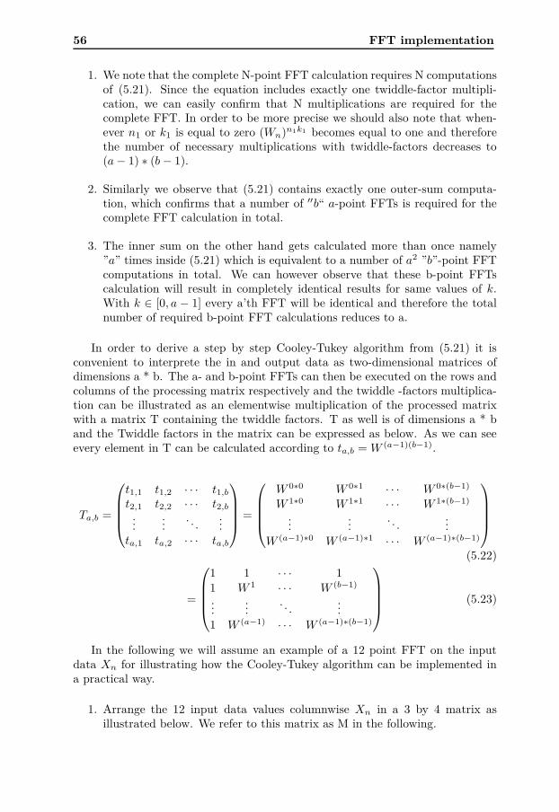
56 FFT implementation
1. We note that the complete N-point FFT calculation requires N computationsof (5.21). Since the equation includes exactly one twiddle-factor multipli-cation, we can easily confirm that N multiplications are required for thecomplete FFT. In order to be more precise we should also note that when-ever n1 or k1 is equal to zero (Wn)n1k1 becomes equal to one and thereforethe number of necessary multiplications with twiddle-factors decreases to(a − 1) ∗ (b − 1).
2. Similarly we observe that (5.21) contains exactly one outer-sum computa-tion, which confirms that a number of ′′b“ a-point FFTs is required for thecomplete FFT calculation in total.
3. The inner sum on the other hand gets calculated more than once namely”a” times inside (5.21) which is equivalent to a number of a2 ”b”-point FFTcomputations in total. We can however observe that these b-point FFTscalculation will result in completely identical results for same values of k.With k ∈ [0, a − 1] every a’th FFT will be identical and therefore the totalnumber of required b-point FFT calculations reduces to a.
In order to derive a step by step Cooley-Tukey algorithm from (5.21) it isconvenient to interprete the in and output data as two-dimensional matrices ofdimensions a * b. The a- and b-point FFTs can then be executed on the rows andcolumns of the processing matrix respectively and the twiddle -factors multiplica-tion can be illustrated as an elementwise multiplication of the processed matrixwith a matrix T containing the twiddle factors. T as well is of dimensions a * band the Twiddle factors in the matrix can be expressed as below. As we can seeevery element in T can be calculated according to ta,b = W (a−1)(b−1).
Ta,b =
t1,1 t1,2 · · · t1,b
t2,1 t2,2 · · · t2,b
......
. . ....
ta,1 ta,2 · · · ta,b
=
W 0∗0 W 0∗1 · · · W 0∗(b−1)
W 1∗0 W 1∗1 · · · W 1∗(b−1)
......
. . ....
W (a−1)∗0 W (a−1)∗1 · · · W (a−1)∗(b−1)
(5.22)
=
1 1 · · · 1
1 W 1 · · · W (b−1)
......
. . ....
1 W (a−1) · · · W (a−1)∗(b−1)
(5.23)
In the following we will assume an example of a 12 point FFT on the inputdata Xn for illustrating how the Cooley-Tukey algorithm can be implemented ina practical way.
1. Arrange the 12 input data values columnwise Xn in a 3 by 4 matrix asillustrated below. We refer to this matrix as M in the following.

5.2 Fast Fourier Transformation 57
Xn →
X1 X5 X9
X2 X6 X10
X3 X7 X11
X4 X8 X12
= M
2. Compute a 3-point FFT for each row of M. We define the resulting valuesto be named as Xn and the resulting Matrix as M .
M =
X1 X5 X9
X2 X6 X10
X3 X7 X11
X4 X8 X12
F F T s−−−−→
X1 X5 X9
X2 X6 X10
X3 X7 X11
X4 X8 X12
= M
3. Elementwise multiplication of M with the matrix T, containing the twiddlefactors. We define the operator ⊛ to represent elementwise multiplication ofmatrices.
M ⊛ T = M ⊛
1 1 1
1 w w2
1 w2 w4
1 w3 w6
=
X1 X5 X9
X2 X6w X10w2
X3 X7w2 X11w4
X4 X8w3 X12w6
4. Compute a 4-point FFT for each column of the matrix M ⊛T . The resultingmatrix Yout contains the scrambled output sequence Yn = FFT (Xn).
X1 X5 X9
X2 X6w X10w2
X3 X7w2 X11w4
X4 X8w3 X12w6
F F T s−−−−→
Y1 Y2 Y3
Y4 Y5 Y6
Y7 Y8 Y9
Y10 Y11 Y12
= Yout

58 FFT implementation
5. Read out the data contained in Yout on a row by row basis for obtaining theordered output sequence Yn.
Y1 Y2 Y3
Y4 Y5 Y6
Y7 Y8 Y9
Y10 Y11 Y12
→ Y1, Y2, Y3, ..., Y12
While the implementation of the algorithm is as we can see relatively simplefor FFTs consisting of two layers, it can get rather complicated for FFTs consistingof multiple layers.
We can conclude from the previous discussion, that the main challenges inimplementing the 300 point FFT where suitable data arrangements in all layers,which allowed for parallel vector computations, on the one hand, and rapid imple-mentations of 5-point and 3-point FFTs (radix-5 and radix-3 computation kernels)on the other hand.
5.2.2 Radix-4 and Radix-2 FFTs
In table 5.1 we gave some example for computational costs savings achieved byusing the Cooley Tukey algorithm. However we still need to discuss another aspectof the algorithm, which concerns FFTs of length two and four, and which leads toeven bigger computational cost savings whenever certain layers consist of smallerFFTs of these two specific lengths. If we take another look at equations (5.16)and (5.17) for calculating an N-point FFT we can easily verify, that if N = 2 orN = 4 the exponential factor (WN )kn = e−2πikn/N can in all cases be simplifiedto one of the following values: e0 = 1, ei π
2 = i, eiπ = −1 and ei 3π2 = −i. This
means that for FFTs of lengths two or four, the multiplications with the term(WN )kn can be replaced by additions and subtractions of the real and imaginaryparts of the input data, which obviously will reduce the computational complexityeven further. Due to this property the most rapid Cooley- Tukey algorithms thatcan be implemented are the so called radix-4 and radix-2 FFTs for FFT lengthswhere N can be factorized exclusively into the numbers 4 or 2 or combinationsof the two. For this reason the computation of for example a 300 point FFT(N = 52 ∗ 3 ∗ 4) cannot be executed at the same speed as a 256-point (N = 44)or even a 512-point FFT (N = 44 ∗ 2). We should furthermore note here that theradix-4 and radix-2 computations in FFT computations are typicaly also referredto as butterfly operations due to the shape of the data-flow diagram with whichthe FFTs can be illustrated.
5.3 300 point FFT Implementation for Sleipnir
The 300 point FFT implementation for the sleipnir SIMD processor was a majortask of this thesis work. When implementing the 300 point FFT for the sleipnirprocessor Matlab has been used as assisting tool throughout the process. It wasused for development and verification of the Cooley Tukey algorithm, computation

5.3 300 point FFT Implementation for Sleipnir 59
of twiddle factors, and verifying the intermediate results during the algorithmimplementation for the SIMD processor. The algorithm has been developed forthe input data type ”complex word“, means for complex data with 16 bit real andimaginary parts, so that four complex data values can be stored in one 128-bitvector.
5.3.1 Cycle cost estimations
In this section we will calculate a lower bound for the clock cycle time needed forrunning the 300 point FFT-algorithm on the sleipnir. As basis for this calculationwe will consider the pure processing time of the computational instructions whichwere used in our approach towards this algorithm implementation. Any additionalprocessing time caused by for example addressing operations, data movementsbetween different memory components or delays due to data-dependencies willbe neglected. This lower bound cycle cost estimation will serve us as a basis forevaluating the actual cycle cost that has been achieved for the sleipnir processor.
The 512 point FFT, which is needed as well in this thesis work, has got anexecution duration of around 900 clock cycles. For the 300 point FFT, despiteof its shorter length, a longer execution time was to be expected because of itsthree layers that do not consist of radix-4 or radix-2 instructions. Due to thebutterfly instructions included in the sleipnir instruction set, a complete 4-pointFFT (radix-4 operation) can be computed in merely one clock cycle effectively.We recall that the 300-point FFT algorithm consists of two layers of radix-5, onelayer of radix-3 and one layer of radix-4 computations. The layers with radix-5calculations were expected to add longer execution times to the algorithm than theother layers. Thus it has been decided to start with radix-5 computations in thefirst layer, as this is the only layer that does not require any multiplication withtwiddle factors. The estimated cycle costs of the different layers will be discussedin the following.
First layer of FFT algorithm
With a total FFT length of 300, a number of 60 5-point FFTs had to be calculatedin each of the first two layers of the algorithm. From (5.17) we can see that one5-point FFT requires the computation of 25 complex multiplications (mulC) and20 complex additions (addC). Taking into account all the cases where the factor(WN )kn is equal to one (which is the case for n = 0 or k = 0) the number of nontrivial complex multiplications decreases to 16 and we get the following expressionfor the total number of complex operations for one 5-point FFT computation,which we refer to as opRadix5:
opRadix5 = 4 ∗ (4 ∗ mulC + 4 ∗ addC) + 4 ∗ addC (5.24)
Since the sleipnir is a SIMD processor, the computations should be executed ondata vectors for optimum performance and speed. As mentioned earlier eachvector can contain up to four complex data values referred to as complex words asit was illustrated in Figure 4.4. The instrcutions which were used for the complex

60 FFT implementation
additions were addw or addwq depending on the fact if the situation requiredfast results or high parallization. One addw instruction can handle the additionof four complex words per clock cycle. For the complex multiplications tcmacwinstructions have been used, which can compute four complex word multiplicationsand accumulate these four results together. Thus tcmacw instructions can executefour complex word multiplications and three complex word additions per clockcycle. We can then compute the total number of instructions needed for the firstlayer of the FFT processing as:
operP erRadix5 = 4 ∗ (4 ∗ mulC + 3 ∗ addC)︸ ︷︷ ︸
1 tcmacw instr.
+ 8 ∗ addC︸ ︷︷ ︸
1 addw instr.
(5.25)
nrInstl1 = 60 ∗ (4 ∗ tcmacw + 8 ∗addw
8) = 240 ∗ tcmacw + 60 ∗ addw (5.26)
Since each of these two instruction types included in the processing can be is-sued once per clock cycle our estimated minimum execution time for the processingin the first stage of the algorithm is equal to 240 + 60 = 300 clock cycles.
Second layer of FFT algorithm
The second layer of processing is very similar to the first layer since it containsas well 60 computations of 5-point FFTs. The execution time for this part cantherefore also be estimated as 300. However, there is an additional computationalstep, which has to be performed in the second stage and that is the multiplicationwith twiddle factors. We could initially assume here that all 300 complex valueswould need to be multiplied with twiddle factors, however as mentioned earliersome of the twiddle factors are tivial having the value one. Since we are in thesecond stage of the algorithm with the second layer of radix-5 computations we caninterpret the computations at this step as the calculation of a number of twelve25-point FFT computations and thus the number of complex multiplications withtwiddle factors reduces to 12*4*4=192 (compare (5.21) ), which can be calculatedby 192
4 = 48 complex word vector multiplications. Thus the minimum estimatedprocessing time for layer 2 is equal to 300 + 48 = 348 clock cycles.
Third layer of FFT algorithm
Layer three of the algorithm consists of a number of hundred radix-3 computations.From (5.17) we can easily verify that one radix-3 computation requires 9 complexmultiplications and 6 complex additions in total. Again some of the multiplicationsare trivial, which reduces the total number of mulC operations. However for thislayer it has been decided to combine the twiddle factors with the exponentialfactors used in the radix-3 computations. This means that these two factors havebeen multiplied together in advance, so that no extra multiplication with twiddlefactors is necessary in this layer. Therefore the complex multiplications are onlytrivial in cases where both the twiddle-factor as well as the radix-3 exponentfactor (WN )kn are equal to one. This is the case for 3 of the nine multiplications,

5.3 300 point FFT Implementation for Sleipnir 61
reducing the total number of operations for one 3-point FFT computation to 6complex multiplications and 6 complex additions.
Again sleipnir tmac-instructions, capable of complex multiplication and resultaccumulation have been used for the implementation. But since in this layer onlytwo results of complex word multiplications need to be accumulated (and not fouras in the radix-5 layers) the instruction tcmacdbw has been used instead. Oneof these instructions is able to execute two times the addition of the results oftwo complex word multiplications. Thus the instruction will be able to handle 4complex word multiplications and 2 complex additions. We can now calculate thetotal number of instructions needed for layer 3 as follows:
operP erRadix3 = 6 ∗ mulC + 6 ∗ addC = 3 ∗ (2 ∗ mulC + 1 ∗ addC)︸ ︷︷ ︸
1/2 tcmacdbw
+3 ∗ addc︸︷︷︸
addw/8
(5.27)
nrInstl3 = 100 ∗ (3 ∗tcmacdbw
2+ 3 ∗
addw
8) = 150 ∗ tcmacdbw+ 38 ∗ addw (5.28)
We see that a total of 225 instruction is needed for the computations includedin layer 3. Neverless the estimated cycle cost is higher than that, due to the factthat it is not possible to issue one tcmacdbw instruction in each clock cycle. Sincewe included the complex twiddle factor multiplications the number of complexmultipliers is too large for being saved in the constant memory. Thus both sourceoperands are fetched from LVMs and the destination is located in the LVMs as well.As mentioned before in each cycle it is only possible to access the LVMs exactly twotimes, one time for reading data from them and one time for writting data intothem. Therefore the tcmacdbw instructions can merely be issued every secondclock cycle and the estimated number of clock cycles for layer 3 computationsincreases to: nrCyclesL3 = 2 ∗ 150 + 75 = 375
Fourth layer of FFT algorithm
Since this layer only consists of radix-4 operations it was relatively straightforwardto be implemented for the sleipnir. As mentioned earlier one complete radix-4operation can be calculated by just one butterfly operation in the ePUMA whichare referred to as cr4bf in the sleipnir assembly code (cr4bf stands for complexradix-4 butterfly). Since layer 4 requires a number of 75 radix-4 computations thesleipnir is able to compute this layer with 75 instructions. As it has been the casein layer 3, due to the limitations of the LVM accessibility, each of these instructionscan only be issued every second clock cycle and thus the estimated cycle cost forlayer 4 is equal to 150 clock-cycles.
5.3.2 Assembly implementation
The complete assembly code of the 300-point FFT algorithm, that has been de-veloped for the sleipnir can be seen in appendix X. Since the code got relativelylong it has been split up into four parts according to the different layers of the

62 FFT implementation
algorithm. Due to the fact that it would take too long to discuss every singlestep of the kernel in detail, we will rather focuss on explaining some specific codeexamples and the challenges, that were faced during the implementation.
The following code example 5.1 shows the tcmacw instructions which havebeen used in layer 1. The repeat command in line 1 means, that the following 15lines will be executed four times. Thus we can easily verify that a total number of240 tcmacw instructions will be issued in this code example, which matches theestimation for layer 1 in the previous section. The operands, which are saved inthe LVM referred to by m0, are the input data values to the FFT algorithm. Theoperands stored in the constant memory have been precalculated in Matlab andrepresent the exponential factors (WN )kn necessary for radix-5 computations.
We can see that this section does not include a single nop operation and thatone tcmacw instruction is issued every clock cycle. Therefore this part of the FFTalgorithm, which represents a big part of the total computational cost, could nothave been implemented in a faster way for the sleipnir processor. The possibility ofissuing one instruction every clock cycle is achieved by using the constant memoryfor one of the operands rather than the LVM for both operands. Therefore theLVM limitation of being only accessible twice per clock cycle does not affect thenumber of instructions per clock cycle in a negative way.
Listing 5.1. radix-5 computations in layer1
1 repeat 15 42 5∗tcmacw <c l r , ss , sat , div=1>3 m1[ ar1 +=2].d m0[ ar0 +cm[ car0 +=1%]].v cm[ r5twid1 ]4 5∗tcmacw <..> m1[ ar1 +=2].d m0[ ar0 +cm [ . . ] ] . v cm[ r5twid2 ]5 5∗tcmacw <..> m1[ ar1 +=2].d m0[ ar0 +cm [ . . ] ] . v cm[ r5twid3 ]6 4∗tcmacw <..> m1[ ar1 +=2].d m0[ ar0 +cm [ . . ] ] . v cm[ r5twid4 ]7 tcmacw <..> m1[ ar1+=s ] . d m0[ ar0+=8 +cm [ . . ] ] . v cm[ r5twid4 ]89 5∗tcmacw <..> m1[ ar1 +=2].d m0[ ar0 +cm [ . . ] ] . v cm[ r5twid1 ]
10 5∗tcmacw <..> m1[ ar1 +=2].d m0[ ar0 +cm [ . . ] ] . v cm[ r5twid2 ]11 5∗tcmacw <..> m1[ ar1 +=2].d m0[ ar0 +cm [ . . ] ] . v cm[ r5twid3 ]12 4∗tcmacw <..> m1[ ar1 +=2].d m0[ ar0 +cm [ . . ] ] . v cm[ r5twid4 ]13 tcmacw <..> m1[ ar1+=s ] . d m0[ ar0+=8 +cm [ . . ] ] . v cm[ r5twid4 ]1415 5∗tcmacw <..> m1[ ar1 +=2].d m0[ ar0 +cm [ . . ] ] . v cm[ r5twid1 ]16 5∗tcmacw <..> m1[ ar1 +=2].d m0[ ar0 +cm [ . . ] ] . v cm[ r5twid2 ]17 5∗tcmacw <..> m1[ ar1 +=2].d m0[ ar0 +cm [ . . ] ] . v cm[ r5twid3 ]18 4∗tcmacw <..> m1[ ar1 +=2].d m0[ ar0 +cm [ . . ] ] . v cm[ r5twid4 ]19 tcmacw <..> m1[ ar1+=s ] . d m0[ ar0+=s% +cm [ . . ] ] . v cm[ r5twid4 ]
We should also note here that in order to allow for a faster execution time, theinput data to the FFT algorithm had to be loaded into the LVM with four gapsof 32 bits which separated the input data values into five blocks of 60 complexdata-values each. This was necessary for circumventing the need of rearranging

5.3 300 point FFT Implementation for Sleipnir 63
the data before algorithm execution in order to allow for vectorized instructionswithout memory-bank conflicts. Obviously the data had to be arranged in suitableways as well in between different layers in order to satisfy both memory bankrequirements of the output of the previously processed layer as well as of the inputdata to the following processing layer.
The following listing 5.1 contains the complete implementation of the fourthlayer of the algorithm which contains the 75 radix-4 butterfly instructions. Aswe can see the actual cycle cost matches the estimated cycle cost exactly for thislayer. When we compare this code of the fourth layer with the overall length ofthe 300 point FFT algorithm, it becomes obvious that the implementation of FFTalgorithms containing non-radix4/radix-2 layers is a significantly bigger challengefor the sleipnir than implementing radix-2/radix-4 FFT algorithms.
Listing 5.2. layer4 implementation
1 repeat 2 752 cr4bf<ss , rnd , sat> m1[ ar0+=2 + cm[ s h i f t l 4 ] ] . v3 m0[ ar1+=2 + cm[ s h i f t l 4 ] ] . v m1 [ ar2 +=8].v4 1∗nop
5.3.3 Cycle costs
The lower bound for the cycle cost on the sleipnir can be calculated by summingup the previously estimated cycle costs of the four layers different layers as follows:
Lowerbound = 300 + 348 + 375 + 150 = 1173 (5.29)
In the result chapter we will present the actual cycle cost that has been achievedfor the FFT implementation and discuss the various factors that limit the executionspeed of the processor.


Chapter 6
Implementing the channelequalization
In the following chapter we will describe how the channel estimation and zero-forcing equalization has been implemented for the sleipnir processor. The algo-rithm has been realized by a number of consecutive computational steps that willbe presented in the following.
6.1 Implementing the computation of the channelestimate
In order to calculate the complex channel estimates it was first necessary to extractfrom the received signal the complex reference symbols transmitted in the fourthOFDM symbol. We shall denote the received reference symbol sequence of length300 as Y refk. The transmitted reference symbol sequence Xrefk is known at thereceiver side. We can thus calculate the complex channel estimates Hk as:
Hk =Y refk
Xrefkk ∈ [0, 299] (6.1)
Instead of dividing the received symbols by the known transmitted reference sym-bols, which would have required 300 complex divisions, the reciprocals of theReference sequence (Xrefk)−1 have been pre-calculated in Matlab, and thus thecomputation of the 300 complex channel estimates can be reduced to 300 complexmultiplications.
Hk = Y refk ∗ (Xrefk)−1 k ∈ [0, 299] (6.2)
The reciprocals of the reference symbol sequence have been loaded into the localvector memory before starting the algorithm execution. Since the sleipnir’s vectoroperations support 4 complex multiplications per clock cycle we might assumehere, that the computation of the 300 complex channel estimates could be realizedin 75 clock cycles. The listing 6.1 shows the actual sleipnir kernel implementation.
65

66 Implementing the channel equalization
Listing 6.1. Channel estimate computation
1 channe l e s t imat i on :23 copy ar0c cm[AR0b]4 dcopy ar1c cm[AR1b]5 dcopy ar2c cm[AR2b]6 4∗nop78 repeat 2 379 cmulwww <rnd , ss , mul=2>
10 m0[ ar0 +=8].v m1[ ar1 +=8].v m0[ ar2 +=8].v11 nop1213 cmulwww <..> m0[ ar0 +=4].h m1[ ar1+=8%].h m0[ ar2 +=4].h14 nop1516 repeat 2 3717 nop18 cmulwww <..> m0[ ar0 +=8].v m1[ ar1 +=8].v m0[ ar2 +=8].v1920 nop21 cmulwww <..> m0[ ar0+=4%].h m1[ ar1+=s %].h m0[ ar2+=4%].h
After this code has been executed, the LVM referred to by m0 contains the300 complex channel estimates Hk. We can observe from the code, that a totalof 76 complex multiplication instructions are executed instead of 75. We neededone instruction more because two half word-instructions had to be included. Thereason for this is, that there exists a gap of half a vector in the middle of thedata after the 512-point FFT algorithm execution, which is needed in order toavoid memory bank conflicts. Additionally we can see that a nop instructionis required between two consecutive cmulwww instructions which consequentlyincreases the cycle cost by a factor of two. As it already has been the case forthe FFT implementation, the limiting factor here is, that only two LVMs canbe accessed per clock cycle, one for reading and one for writing. And since thereference symbol sequence is with a length of 300 too large for being stored in theconstant memory, both source operands as well as the destination of the cmulwwwinstructions have to be LVMs, which makes the nop operations necessary. Inconclusion the channel estimate computation requires 152 clock cycles plus a fewextra cycles for addressing purposes.
6.2 Implementing the zero-forcing equalizer
For the equalization of the received data-symbols, there are different alternativeshow the channel estimates can be used. The simplest approach, which has been

6.2 Implementing the zero-forcing equalizer 67
used in this thesis, is to assume the channel estimates to remain relatively con-stant over the duration of one time-slot. This means that the channel estimates,calculated by using the reference symbols in the fourth OFDM symbol of the slot,will be used for equalization of the six surrounding OFDM symbols of the slot,which contain data. Alternative enhanced channel estimation methods would in-clude averaging or interpolation between consecutive channel estimates in order topotentially gain even more accurate channel estimates for the equalization of theOFDM data symbols. Naturally the benefit of these different methods depends onthe channel conditions and the coherence time of the channel in particular. Bothaveraging and interpolation methods have not been considered in this thesis. It isworth mentioning, that the approach that has been chosen for the project imple-mentation can be considered sufficient for the majority of radio-channel scenarios.Since the time duration of a slot is with 0.5 ms relatively short, interpolationbetween channel estimates of consecutive slots for instance can only be expectedto give substantial throughput gains in certain special scenarios like for exam-ple for very fast moving mobile users, which would correspond to a very shortchannel-coherence time.
The zero-forcing equalization can then be realized according to the followingequation,
Xk = Yk ∗ Hk−1
= Yk ∗1
ˆ|Hk|2 ∗
¯Hk
︸ ︷︷ ︸
Equalization factor
(6.3)
where Xk represents the equalized complex symbol sequence, and Yk denotesthe received data symbol sequence that shall be equalized.
The term referred to as “equalization factor” in 6.3 only needs to be calculatedone time for each slot, and its result will then be multiplied with the data sequencesof all six OFDM-Data symbols within the slot. In the sleipnir the computation ofthis equalization factor has then been realized by executing the following steps:
1. Compute the 300 complex channel estimates Hk
2. Calculate the complex conjugate of the estimates¯
Hk
3. Calculate the square of the absolute value of the estimates ˆ|Hk|2
by multi-
plying Hk with¯
Hk
4. Computing the reciprocal of the result, 1ˆ|Hk|
2
5. Multiplying the complex conjugates¯
Hk with the reciprocals 1ˆ|Hk|
2
While the implementation of most of these steps is relatively straightforwardfor the sleipnir processor, the division in step 4 needs an additional algorithm,since the sleipnir, as mentioned before, does not support instructions for division,due to its fixed point architecture.

68 Implementing the channel equalization
6.2.1 Kernel for 1/x
The division 1/x has been implemented with a kernel that has been investigatedfor the ePUMA SIMD co-processors in [19]. The kernel uses a polynomial approx-imation as follows:
1
x≈ 1.2307 − 1.5166y + 1.8691y2 − 2.1248y3 + 2.8013y4 − 7.0989y5 (6.4)
with y = x − 0.8125 and x ∈ [0.5, 1] For details regarding how this polynomialapproximation can be derived the reader is referred to [19]. We can see that it isnecessary to subtract the value 0.8125 from the input to the reciprocal algorithm,and that the approximation is valid for input values within the interval 0.5 to 1.In our case for problem simplification we chose a channel transfer function, whichallowed the results from the 512-point FFT algorithm to be scalable in such a waythat they lay inside this range between 0.5 and 1.
6.2.2 Assembly code and cycle cost
The following listing 6.2 shows how the computation of ˆ|Hk|2
has been imple-mented for the sleipnir processor, which corresponds to step 2 and 3 of the earlierlisted algorithm steps.
Listing 6.2. Channel equalization 1
1 dcopy ar1c cm[ AR0c ]2 dcopy ar3c cm[ AR3a ]34 repeat 10 9 // execute the next 10 l i n e s 9 times5 8∗dcopy v r f [ ra r0 =0 ,+=8].v m0[ ar0 +=8].v6 1∗nop7 cmulwww <rnd , ss , mul=2, conj> m1[ ar1+=s ] . v8 v r f [ ra r0 +=8].v m0[ ar2 +=8].v9 cmulwww <..> m1[ ar3+=s ] . v v r f [ ra r0 +=8].v m0[ ar2 +=8].v
10 cmulwww <..> m1[ ar1+=s ] . v v r f [ ra r0 +=8].v m0[ ar2 +=8].v11 cmulwww <..> m1[ ar3+=s ] . v v r f [ ra r0 +=8].v m0[ ar2 +=8].v12 cmulwww <..> m1[ ar1+=s ] . v v r f [ ra r0 +=8].v m0[ ar2 +=8].v13 cmulwww <..> m1[ ar3+=s ] . v v r f [ ra r0 +=8].v m0[ ar2 +=8].v14 cmulwww <..> m1[ ar1+=s ] . v v r f [ ra r0 +=8].v m0[ ar2 +=8].v15 cmulwww <..> m1[ ar3+=s ] . v v r f [ ra r0 +=8].v m0[ ar2 +=8].v16 ///////// end repeat (72 out o f 75 v e c t o r s are f i n i s h e d )1718 3∗dcopy v r f [ ra r0 =0 ,+=8].v m0[ ar0 +=8].v19 1∗nop20 cmulwww <..> m1[ ar1+=s ] . v v r f [ ra r0 =0 ,+=8].v m0[ ar2 +=8].v21 cmulwww <..> m1[ ar3+=s ] . v v r f [ ra r0 +=8].v m0[ ar2 +=8].v

6.2 Implementing the zero-forcing equalizer 69
22 cmulwww <..> m1[ ar1+=s %].v v r f [ ra r0 +=8].v m0[ ar2 +=8].v2324 //// Al l abs (h^2) va lue s are now s to r ed in m1.
The input to the algorithm are the 300 complex channel estimates, stored inthe LVM “m0”. The algorithm first copies as many of these values as possible intothe vector register file (VRF). Afterwards the values in the VRF are multipliedwith the identical values that are still stored in the LVM “m0” with the option“conj” activated. This option means that the complex conjugate of the secondoperand will be used as input for the multiplication. We recall that for a complexNumber Z with its complex conjugate Z the following equation holds:
Z ∗ Z = |Z|2 (6.5)
Thus after execution of the code in listing 6.2, the LVM “m1” contains the squareof the absolute value of the channel estimates which is the input to the reciprocalcomputing algorithm that is presented in the next code example.
As we can see in listing 6.3 the data first gets scaled to match the input rangebetween [0.5, 1] before the value 0.8125 gets subtracted for polynomial approx-imation. The polynomial approximation is executed in the vector register filefor eight complex values during each loop iteration. The algorithm uses the in-struction mulfbwww which stands for “multiplication feedback”. This operationexecutes a multiplication in which one operand is the result of a multiplication inthe previous cycle. This instruction is very suitable for polynomial computation,because no nop operations are necessary between computations of different expo-nents of the input value. After the mulfbwww instructions have been executed theVRF contains the values y, y2, y3, y4 and y5 for each of the eight input valuesy = x − 0.8125. Furthermore these values have been permuted in such a way thatfor each of the eight polynomials all its exponential values can be accessed simulta-neously. The polynomial coefficients are stored in the constant memory (referredto as Coeff in the code) and the computation of the polynomials has been realizedby usage of tmacw instructions.
Listing 6.3. Channel equalization 2
1 // s c a l i n g the data in to the range [ 0 . 5 , 1 ]2 37∗cmulwww <rnd , ss , mul=2>3 m0[ ar0 +=8].v m1[ ar1+=s+cm[ v2 ] ] . v cm[ s c a l e 1 ]4 cmulwww <..> m0[ ar0 +=8].v m1[ ar1+=8+cm[ v2 ] ] . v cm[ s c a l e 1 ]5 7∗nop67 // subt ra c t va lue 0 .8125 f o r polynomial aproximation8 38∗addw <s , sat , rnd , div=0> m1[ ar1 +=8].v m0[ ar2 +=8].v cm[ subb ]9
10 //Setup a d r e s s i n g r e g i s t e r s11 dcopy vr0 cm[ ones ]12 dcopy ar0c cm [AR0d]

70 Implementing the channel equalization
13 dcopy ar3c cm[ AR0a ]14 dcopy ar1c cm[ AR0a ]15 2∗nop1617 repeat 24 38 // execute f o l l o w i n g 24 l i n e s f o r 38 times18 dcopy vr7 m1[ ar0 +=8].v19 1∗nop20 mulwww <rnd , sat , ss , mul=1>21 v r f [ ra r0=8,+=8 +cm[PTT1 ] ] . v vr7 cm[ ones ]22 mulfbwww <rnd , sat , s , mul=1> v r f [ ra r0+=8+cm [PTT2 ] ] . v vr723 mulfbwww <rnd , sat , s , mul=1> v r f [ ra r0+=8+cm [PTT3 ] ] . v vr724 mulfbwww <rnd , sat , s , mul=1> v r f [ ra r0+=8+cm [PTT4 ] ] . v vr725 mulfbwww <rnd , sat , s , mul=1> v r f [ ra r0+=8+cm [PTT5 ] ] . v vr726 6∗nop27 tmacw <rnd , sat , ss , mul=2, c l r >28 vr6 . 0 v r f [ ra r0=0+cm[PPT1 ] ] . v cm [ Coe f f ]29 tmacw <... > vr6 . 1 v r f [ ra r0=0+cm[PPT2 ] ] . v cm [ Coe f f ]30 tmacw <... > vr6 . 2 v r f [ ra r0=0+cm[PPT3 ] ] . v cm [ Coe f f ]31 tmacw <... > vr6 . 3 v r f [ ra r0=0+cm[PPT4 ] ] . v cm [ Coe f f ]32 tmacw <... > vr6 . 4 v r f [ ra r0=0+cm[PPT5 ] ] . v cm [ Coe f f ]33 tmacw <... > vr6 . 5 v r f [ ra r0=0+cm[PPT6 ] ] . v cm [ Coe f f ]34 tmacw <... > vr6 . 6 v r f [ ra r0=0+cm[PPT7 ] ] . v cm [ Coe f f ]35 tmacw <... > vr6 . 7 v r f [ ra r0=0+cm[PPT8 ] ] . v cm [ Coe f f ]36 5∗nop37 dcopy vr3 cm[ ze r o s ]38 dcopy v r f [ ra r0 =33] . v cm[ ze r o s ]3940 // Sca l ing r e s u l t s back to o r i g i n a l range41 cmulwww <rnd , ss , mul=2> v r f [ ra r0=24 +cm [ pt1 ] ] . v42 vr6 cm [ s c a l e 1 ]43 //At t h i s po int e i g h t va lue s o f "1/ abs (h ) " are s to r ed in44 // vr3 and vr4 , which s t i l l have to be m u l t i p l i e d with h∗4546 6∗nop47 cmulwww <rnd , ss , mul=2, conj> m1[ ar1 +=8].v vr3 m0[ ar3 +=8].v48 cmulwww <rnd , ss , mul=2, conj> m1[ ar1 +=8].v v r f [ ra r0 =33] . v49 m0[ ar3 +=8].v50 1∗nop51 //end o f repeat
We should furthermore note here that this loop computes in total 38 ∗ 8 = 304values while only 300 equalization factors need to be calculated. The 4 additionalvalues that get computed are garbage values that appear due to the vectorizedoperations of the algorithm, since in the last loop execution only 4 values areleft to be computed. It might be possible to achieve a minimal improvement incomputational cost if we would replace the last (the 38th) loop iteration with

6.3 Cycle cost 71
other code that only computes four values instead of eight. However the potentialbenefit in cycle cost would not even reach 10 clock cycles and thus it did not seemreasonable to introduce the redundant code lines that would have been necessaryfor this purpose.
6.3 Cycle cost
The total implementation cost of the channel equalization algorithm is 1854 cycles.This number consists of 159 cycles for computation of the channel estimates and1695 cycles for the computation of the equalization factors.
We can see from this channel equalizer implementation that the restriction ofhaving only two accessible LVM’s per clock cycle significantly limits the overallexecution time of algorithms on the sleipnir-processor. As we will further discussin the following chapter on the example of the 300 point FFT kernel, a largerconstant memory or the possibility of accessing three LVMs per clock cycle, wouldgreatly increase the overall execution speed of algorithms on the sleipnir processor.

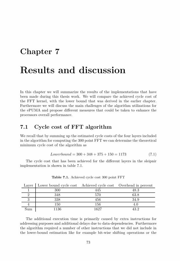
Chapter 7
Results and discussion
In this chapter we will summarize the results of the implementations that havebeen made during this thesis work. We will compare the achieved cycle cost ofthe FFT kernel, with the lower bound that was derived in the earlier chapter.Furthermore we will discuss the main challenges of the algorithm utilizations forthe ePUMA and propose different measures that could be taken to enhance theprocessors overall performance.
7.1 Cycle cost of FFT algorithm
We recall that by summing up the estimated cycle costs of the four layers includedin the algorithm for computing the 300 point FFT we can determine the theoreticalminimum cycle cost of the algorithm as
Lowerbound = 300 + 348 + 375 + 150 = 1173 (7.1)
The cycle cost that has been achieved for the different layers in the sleipnirimplementation is shown in table 7.1.
Table 7.1. Achieved cycle cost 300 point FFT
Layer Lower bound cycle cost Achieved cycle cost Overhead in percent1 300 445 48.32 348 570 63.83 338 456 34.94 150 156 4.0
Sum 1136 1627 43.2
The additional execution time is primarily caused by extra instructions foraddressing purposes and additional delays due to data-dependencies. Furthermorethe algorithm required a number of other instructions that we did not include inthe lower-bound estimation like for example bit-wise shifting operations or the
73

74 Results and discussion
movements of data between different memory components like LVMs and VRF. Wecan see that the percentage in overhead varies significantly between the differentprocessing layers. This does not come as a surprise since the amount of overheadcompared to the lower bound increases with higher complexity of the processinglayer regarding to computation, data arrangements and addressing patterns.
7.2 Evaluation of the results
In order to evaluate the performance of the FFT implementation, presented inthis work, we are going to compare the achieved cycle cost to several other FFTimplementations in the following. In [16] three non-power-of-two point FFTs havebeen implemented for the ePUMA with sizes 1152, 1200 and 1536. In order tocompare the cycle cost in [16] with our FFT implementation we will first estimatewhich cycle cost we could expect if we would use the 300 point FFT implementationpresented in this thesis, in order to compute a 1200 point FFT, as such an extensionwould be relatively straightforward.
Applying the Cooley-Tukey algorithm once more we would simply have tocalculate a number of four 300 point FFTs and add one more layer of radix 4operations. With the total FFT length of 1200, this means that we would needan extra number of 300 radix-4 (cr4bf) operations, which could be executed everysecond clock cycle. Assuming an additional overhead of 4 % for this additionallayer (equivalent to the overhead we saw for the radix-4 layer implemented in the300 point FFT) we can compute an estimate for the total cycle cost of an 1200FFT as follows:
Cyclecost(FFT 1200) ≈ 4 ∗ (1627) + (300 ∗ 2) ∗ 1.04 = 6508 + 624 = 7132 (7.2)
The following table shows the cycle costs that have been achieved in [16] andalso the performance for these FFTs on the T1 dedicated FFT co-processor, whichhas also been used in [16] for evaluating the FFT implementations.
Table 7.2. Achieved cycle cost in [16]
FFT size 1152 1200 1536ePUMA (one SIMD) cycle cost in [16] 4074 7657 4296
T1 dedicated FFT co-processor (FFTC) 3026 3063 3795
We can see that our estimated cycle cost of 7132 based on the 300 point FFTimplementation made in this thesis is below the achieved cycle cost for a 1200point FFT in [16], which gives an indication of the efficiency of the FFT imple-mentation done in this thesis work. However, we have to keep in mind that thecycle cost is only an estimate and adressing cost may potentially be somewhathigher when implementing the complete 1200 point FFT in reality. As we can seethe T1 dedicated FFT co-processor shows a better performance in cycle cost, butit also has got more than double the computing ability and resources than one of

7.2 Evaluation of the results 75
ePUMA’s SIMDs [16]. Due to this differences in computing power, the results stillshow a reasonable performance of the ePUMA as an FFT processing unit. Formore details regarding the comparism between ePUMA and the FFTC processor,the readier is referred to [16].
From the cycle cost estimate for the 1200 FFT we can also develop a minimumclock frequency for the ePUMA processor as a baseband processing unit in LTEbase stations.
In [20] the throughput requirements as illustrated in table 7.3 have been usedin order to derive minimum requirement for FFT and IFFT processing units im-plementing the LTE standard.
Table 7.3. Aggregate throughput (TP) performance requirements for 3GPP LTE-Auplink receiver [20]
Standard MIMO scheme TP FFT TP IFFT3GPP LTE-A uplink 4 x 4 427 MS/s 250 MS/s
Future extension for 3GPPwith large-scale MIMO
128 x 8 13.65 GS/s 500 MS/s
We recall that an IFFT of size 1200 is part of the baseband processing chain ofthe biggest transmission bandwidth defined for LTE of 20 MHz. (compare table3.1) As we can see in table 7.3, the required throughput of LTE uplink is 250 Megasymbols per second.
With the same approach as used in [20] we can calculate the maximum pro-cessing time tmax for an FFT of length 1200 as:
tmax =1
250∗106∗1/s1200
= 4.8µs (7.3)
Assuming that one FFT shall be processed by one of ePUMA’s SIMDs we cannow calculate a rough estimate for the minimum clock period that the ePUMAshould operate with in order to handle the IFFT processing for the biggest LTEbandwidth:
tclk =4.8 ∗ 10−6
7132≈ 6.73 ∗ 10−10s (7.4)
And the minmum required clock frequency for the ePUMA can then be calcu-lated as:
fclkmin=
1
6.73 ∗ 10−10s≈ 1.486GHz (7.5)
With an equivlanet computation, and using the clock cycle cost for our imple-mented FFT of length 300, we can determine the minimum clock frequency forprocessing a BW of 5 MHz to be fclkmin
≈ 339MHzUsing different SIMDs for processing various FFTs in parallel, it may how-
ever be possible to execute the neccessary baseband computation steps with evenlower clock frequencies for the ePUMA. Such an approach would naturally cause

76 Results and discussion
extra delays and the question how far the clock frequency could be reduced viaparallelization needs to be further investigated and is not covered by this thesis.
7.3 Challenges of the implementation
The major challenges of this FFT implementation for the ePUMA were relatedto the fact that the different processing layers consisted of different smaller FFTsizes, and thus the layers varied significantly in the way they had to be computed.This fact together with the limitations of the LVMs memory banks accessibilityput a lot of different requirements on the data-arrangements throughout the wholealgorithm. In order to fully utilize the vector-operation potential of the sleipnira big amount of various data-permutation patterns had to be used which had tobe stored in the CM. Furthermore the big number of different data-arrangementsmade many different re-initializations of the special purpose registers for addressingnecessary. The big number of permutation patterns on the one hand and thevarious vectors for address-register initialization on the other hand caused the CMto fill up quite rapidly. In fact the 128 vectors-storage capacity of the CM turnedout to be the bottle-neck during the algorithm-implementation.
Cyclic addressing was used in order to reduce the necessary amount of address-register re-initializations, however the fact that only one step size could be con-figured by the user limited the benefit of this method. The gain of the cyclicaddressing methods with respect to address-register re-initialization efforts couldbe increased significantly if it would be possible to configure a bigger number ofdifferent step sizes for incrementing the address pointers. An option to achievethis would be to remove the standard step-sizes 1,2,4,8 in order to enable the pro-grammer to specify five different step sizes during address-register initializationinstead of only one. That would have been very beneficial during this algorithmimplementation, especially since the step-sizes 1, 2 and 4 have almost never beenused for LVM addressing, due to the fact that vector operations were used most ofthe time. The possibility of using five configurable step sizes would have reducedthe amount of address-register re-initializations and freed up more CM capacityas well.
Additional available CM capacity brings another advantage namely that moreprocessing data like for example in this case Twiddle factors could be stored inthe CM. This can speed up the execution time because computational instructionsincluding one CM operand can be executed twice as often as instructions requiringthree LVM accesses for the two operands and the destination. Due to all previousmentioned facts it might be worth considering if a bigger CM memory might bemore desirable for the sleipnir processor. Of course that would increase the costof the processor as it would also be the case for another potential improvementwhich could be to make the LVMs accessible three times per clock-cycle.
In conclusion we can summarize, that the limitations of the LVMs accessibilityper clock cycle and/or the relatively small size of the CM should probably beaddressed if the ePUMA should work as a processing unit for computational tasksof high complexity like for example baseband processing algorithms. Even if a

7.3 Challenges of the implementation 77
larger CM and a better LVM accessibility should turn out to be too expensiveimprovements, it is strongly proposed to at least give the programmer the flexibilityof specifying more different step sizes for the address register in order to relax therestraints on the sleipnir’s CM capacity.


Chapter 8
Conclusions
In this thesis a simplified model of the LTE uplink receiving chain has been imple-mented in Matlab and parts of it have been mapped onto the ePUMA platform.We however need to keep in mind that from our highly simplified model there isstill a very long way to go to developing a complete working LTE uplink basebandreceiver which could run in LTE base stations. The ePUMA indeed offers a strongcomputational power due to its multi-core SIMD approach and it seems a reason-able assumption, based on the implementations made in this thesis work, that theplatform has the computational potential to handle many of the algorithms used inan LTE base station. However, since the design of an LTE uplink baseband receiveris a very challenging task, wich includes a big number of different algorithms ofhigh complexity, it seems questionable if a platform which only supports assemblylanguage will offer a comfortable enough programming environment for softwaredevelopers in order to finish such an enormous task in reasonable time. A higherlevel language would certainly be desirable when implementing a project of sucha high complexity like an LTE baseband receiver. The problem however is that ahigh level language could not efficiently exploit the full potential of the ePUMAplatform and this puts some restraints on the general potential of the ePUMA forprojects of high complexity. Another problem is, that the strong competition inthe telecommunication field leads to ongoing efforts by vendors to continuouslyimprove the LTE networks performance. Since the LTE standard is constantlyenhanced and improved and base stations are being upgraded all the time by newproduct releases in an iterative process of product improvements it might be avery challenging task for any vendor to completely change the hardware platformfor the baseband processing modules in their base stations.
During the kernel implementation of the 300 point FFT for the SIMD pro-cessors a number of challenges had to be surpassed. A main problem was thatthe algorithm required a lot of different addressing patterns and thus the con-stant memory filled up rapidly. For this specific algorithm development the con-stant memory really appeared to be a bottle-neck of the sleipnir. Based on theexperiences made during the implementation it became clear that the constantmemory allocation used for initialization of special purpose address registers could
79

80 Conclusions
be significantly reduced if more than one step size would have been available forincrementing the pointers stored in the addressing registers. An easy achievableand very beneficial solution would be to allow the specification of five step sizesinstead of having only one configurable step size and the four standard step sizes1,2,4 and 8 since many of them have never or rarely been used in the whole al-gorithm implementation. Another issue worth considering might be to increasethe constant memory size, because a bigger constant memory furthermore allowsfor faster algorithm computations in many circumstances. Since we need to keepin mind the fact that a large constant memory produces high cost, an alternativesolution might be to include SIMDs with different CM sizes in order to provide areasonable trade-off between reducing cost while simultaneously not limiting theplatforms capabilities too much.
8.1 Future work
The work on the ePUMA processor at ISY is currently ongoing. With respect toLTE baseband processing algorithms a lot of different work items can be thoughtoff. It would be possible to further improve the model of the LTE baseband receiverchain implemented in this thesis. Such improvements could for example include thedevelopment of an MMSE equalizer, or the support of a wider range of transmissionbandwidths or investigating different methods of dividing the workloads betweenthe SIMD processors. Furthermore it might be interesting to compare the ePUMAscomputational performance and cost with the actual performance and costs ofthe hardware modules that are used by vendors in their base stations in orderto evaluate the theoretical potential of the ePUMA. Independent of the fact, ifthe ePUMA one day will serve as a processing unit in LTE base stations, theplatform surely has got a very interesting concept, and further investigation of itspotential as LTE base station unit is encouraged, due to the platforms enormouscomputational potential on the one hand and due to the great variety of learningopportunities that such a project offers for students on the other hand.

8.1 Future work 81


Bibliography
[1] Lars Ahlin, Jens Zander, and Slimane Ben Slimane. Principles of wirelesscommunications. 2006.
[2] Raad Farhood Chisab and CK Shukla. Performance evaluation of 4g-lte-scfdma scheme under sui and itu channel models. International Journal ofEngineering & Technology IJET-IJENS February, 2014.
[3] Erik Dahlman, Stefan Parkvall, and Johan Sköld. 4G: LTE/LTE-Advancedfor Mobile Broadband. Academic Press, 1 edition, 2011. ISBN 978-0-12-385489-6.
[4] Erik Dahlman, Stefan Parkvall, Johan Sköld, and Per Beming. 3G Evolution:HSPA and LTE for mobile broadband. Addison-Wesley, 2 edition, 2008. ISBN978-0-12-374538-5.
[5] Johannes Demel, Sebastian Koslowski, and Friedrich K Jondral. A lte receiverframework implementation in gnu radio.
[6] ePUMA research team. Epuma memory subsystem user manual. LinköpingUniversity, Computer Engineering, The Institute of Technology, Version 4.17,27 September 2011.
[7] ePUMA research team. Senior instruction set manual. Linköping Univer-sity, Computer Engineering, The Institute of Technology, Version 4.17, 27September 2011.
[8] ePUMA research team. Sleipnir instruction set manual. Linköping Univer-sity, Computer Engineering, The Institute of Technology, Version 4.17, 27September 2011.
[9] ePUMA research team. Sleipnir programming manual. Linköping Univer-sity, Computer Engineering, The Institute of Technology, Version 4.17, 27September 2011.
[10] Borko Furht and Syed A. Ahson. Long Term Evolution: 3GPP LTE Radioand Cellular Technology. Auerbach, 1 edition, 2009. ISBN 978-1-420-07210-5.
[11] Hari Krishna Garg. Digital Signal Processing Algorithms. CRC Press, 1edition, 1998. ISBN 0-8493-7178-3.
83

84 Bibliography
[12] Andreas Karlsson. Algorithm adaptation and optimization of a novel dsp vec-tor co-processor. Master’s thesis, Master thesis done at Linköping University,Computer Engineering, The Institute of Technology.
[13] Rainer Keller, David Kramer, and Jan-Philipp Weiss. Facing the Multicore-Challenge II: Aspects of New Paradigms and Technologies in Parallel Com-puting. Springer, 1 edition, 2012.
[14] Farooq Khan. LTE for 4G Mobile Broadband. Cambridge, 1 edition, 2009.ISBN 978-0-521-88221-7.
[15] Dake Liu. Embedded DSP Processor Design. Morgan Kaufmann, 1 edition,2008. ISBN 978-0-12-374123-3.
[16] Zhenyu Liu, Qunfang Xie, Hongkai Wang, Yanjun Zhang, and Dake Liu. Ahigh performance implementation of non-power-of-two fft with epuma plat-form. Procedia Engineering, 29:3408–3412, 2012.
[17] Hyung G. Myung and David Goodman. Single Carrier FDMA: A New AirInterface for Long Term Evolution. Wiley, 1 edition, 2008.
[18] Mikael Olofsson. Tables and Formulas for Signal Theory. Studentlitteratur,1 edition, 2011. ISBN 978-91-44-07328-6.
[19] Orri Tómasson. Implementation of elementary functions for a fixed point simddsp coprocessor. Master’s thesis, Master thesis done at Linköping University,Computer Engineering, The Institute of Technology.
[20] Guohui Wang, Bei Yin, Inkeun Cho, Joseph R Cavallaro, Souvik Bhat-tacharyya, and Jarmo Takala. Efficient architecture mapping of fft/ifftfor cognitive radio networks. In Acoustics, Speech and Signal Processing(ICASSP),2014 IEEE International Conference on, pages 3933–3937. IEEE,2014.
[21] Jian Wang, Joar Sohl, Olof Kraigher, and Dake Liu. epuma: A novel embed-ded parallel dsp platform for predictable computing. In Education Technologyand Computer (ICETC), 2010 2nd International Conference on, volume 5,pages V5–32. IEEE, 2010.
[22] H. Joseph Weaver. Applications of discrete and continuous Fourier analysis.Krieger, 2 edition, 1992. ISBN 0-89464-735-0.

Appendix A
Kernel for 300 point FFT
1 FFT300 :2 //////////////////////////////////////////////////////////////////////3 // Layer14 //////////////////////////////////////////////////////////////////////5 dcopy ar0c cm[ AR0a ]6 dcopy ar1c cm[ AR1a ]7 dcopy ar2c cm[ AR1c ]8 dcopy ar3c cm[ AR3a ]9 dcopy car0c cm [ car 0_i n i t ]
10 dcopy car1c cm [ car 1_i n i t ]11 //////////////////////////////////////////////////////////////////////12 4∗ dcopy v r f [ r a r 0 =0, +=8].v m0[ ar0 +=8].v13 4∗ dcopy v r f [ r a r 0 +=8].v m0[ ar1 +=8].v14 3∗addwq <s , sat , rnd , div=1>15 v r f [ r a r 0 =0,+=8]. v v r f [ r a r 1 =0,+=8]. v m0[ ar3 +=8].v16 addwq <..> v r f [ r a r 0 +=8].v v r f [ r a r 1 +=8].v m0[ ar3+=s ] . v17 3∗addwq <s , sat , rnd , div=1> v r f [ r a r 0 +=8].v v r f [ r a r 1 +=8].v m0[ ar3 +=8].v18 addwq <..> v r f [ r a r 0 +=8].v v r f [ r a r 1 +=8].v m0[ ar3+=s %]. v19 3∗nop20 2∗addwq <..> m1[ ar2+=s+cm [ v1 ] ] . v v r f [ r a r 0 =0,+=8]. v v r f [ r a r 1 =32, +=8].v21 addwq <..> m1[ ar2+=s%+cm [ v1 ] ] . v v r f [ r a r 0 +=8].v v r f [ r a r 1 +=8].v22 addwq <..> m1[ ar2+=s+cm [ v1 ] ] . v v r f [ r a r 0 ] . v v r f [ r a r 1 ] . v23 //////////////////////////////////////////////////////////////////////24 4∗ dcopy v r f [ r a r 0 =0,+=8].v m0[ ar0 +=8].v25 4∗ dcopy v r f [ r a r 0 +=8].v m0[ ar1 +=8].v26 3∗addwq <..>27 v r f [ r a r 0 =0,+=8]. v v r f [ r a r 1 =0,+=8]. v m0[ ar3 +=8].v28 addwq <..> v r f [ r a r 0 +=8].v v r f [ r a r 1 +=8].v m0[ ar3+=s ] . v29 3∗addwq <..> v r f [ r a r 0 +=8].v v r f [ r a r 1 +=8].v m0[ ar3 +=8].v30 addwq <..> v r f [ r a r 0 +=8].v v r f [ r a r 1 +=8].v m0[ ar3+=s %]. v31 3∗nop32 addwq <..>33 m1[ ar2+=s+cm [ v1 ] ] . v v r f [ r a r 0 =0, +=8].v v r f [ r a r 1 =32 ,+=8].v34 addwq <..>35 m1[ ar2+=s%+cm [ v1 ] ] . v v r f [ r a r 0 +=8].v v r f [ r a r 1 +=8].v36 2∗addwq <..>37 m1[ ar2+=s+cm [ v1 ] ] . v v r f [ r a r 0 +=8].v v r f [ r a r 1 +=8].v38 //////////////////////////////////////////////////////////////////////39 4∗ dcopy v r f [ r a r 0 =0, +=8].v m0[ ar0 +=8].v40 4∗ dcopy v r f [ r a r 0 +=8].v m0[ ar1 +=8].v41 3∗addwq <..>42 v r f [ r a r 0 =0,+=8]. v v r f [ r a r 1 =0,+=8]. v m0[ ar3 +=8].v43 addwq <..> v r f [ r a r 0 +=8].v v r f [ r a r 1 +=8].v m0[ ar3+=s ] . v44 3∗addwq <..> v r f [ r a r 0 +=8].v v r f [ r a r 1 +=8].v m0[ ar3 +=8].v
85

86 Kernel for 300 point FFT
45 addwq <..> v r f [ r a r 0 +=8].v v r f [ r a r 1 +=8].v m0[ ar3+=s %]. v46 dcopy ar3c cm [ AR3b ]47 2∗nop48 addwq <..>49 m1[ ar2+=s%+cm [ v1 ] ] . v v r f [ r a r 0 =0,+=8]. v v r f [ r a r 1 =32 ,+=8].v50 2∗addwq <..>51 m1[ ar2+=s+cm [ v1 ] ] . v v r f [ r a r 0 +=8].v v r f [ r a r 1 +=8].v52 addwq <..>53 m1[ ar2+=s%+cm [ v1 ] ] . v v r f [ r a r 0 +=8].v v r f [ r a r 1 +=8].v54 //////////////////////////////////////////////////////////////////////55 2∗ dcopy v r f [ r a r 0 =0, +=8].v m0[ ar0 +=8].v56 dcopy v r f [ r a r 0 +=8].v m0[ ar0+=8%].v // ar0 =12257 2∗ dcopy v r f [ r a r 0 +=8].v m0[ ar1 +=8].v58 dcopy v r f [ r a r 0 +=8].v m0[ ar1+=8%].v59 2∗addwq <..>60 v r f [ r a r 0 =0, +=8].v v r f [ r a r 1 =0, +=8].v m0[ ar3 +=8].v61 addwq <..> v r f [ r a r 0 +=8].v v r f [ r a r 1 +=8].v m0[ ar3+=s ] . v62 2∗addwq <..> v r f [ r a r 0 +=8].v v r f [ r a r 1 +=8].v m0[ ar3 +=8].v63 addwq <..> v r f [ r a r 0 +=8].v v r f [ r a r 1 +=8].v m0[ ar3 ] . v64 3∗nop65 2∗addwq <..>66 m1[ ar2+=s+cm[ v1 ] ] . v v r f [ r a r 0 =0, +=8].v v r f [ r a r 1 =24, +=8].v67 addwq <..> m1[ ar2+cm [ v1 ] ] . v v r f [ r a r 0 ] . v v r f [ r a r 1 ] . v68 //////////////////////////////////////////////////////////////////////69 dcopy ar2c cm [ AR1c ]70 dcopy ar3c cm [ AR1c ]71 nop72 r epeat 15 473 5∗tcmacw <c l r , ss , sat , d iv=1>74 m1[ ar1 +=2].d m0[ ar0 +cm [ car0 +=1%]].v cm [ r5twid1 ]75 5∗tcmacw <..> m1[ ar1 +=2].d m0[ ar0 +cm [ car0 +=1%]].v cm [ r5twid2 ]76 5∗tcmacw <..> m1[ ar1 +=2].d m0[ ar0 +cm [ car0 +=1%]].v cm [ r5twid3 ]77 4∗tcmacw <..> m1[ ar1 +=2].d m0[ ar0 +cm [ car0 +=1%]].v cm [ r5twid4 ]78 tcmacw <..> m1[ ar1+=s ] . d m0[ ar0+=8 +cm [ car0 +=1%]].v cm [ r5twid4 ]79 5∗tcmacw <..> m1[ ar1 +=2].d m0[ ar0 +cm [ car0 +=1%]].v cm [ r5twid1 ]80 5∗tcmacw <..> m1[ ar1 +=2].d m0[ ar0 +cm [ car0 +=1%]].v cm [ r5twid2 ]81 5∗tcmacw <..> m1[ ar1 +=2].d m0[ ar0 +cm [ car0 +=1%]].v cm [ r5twid3 ]82 4∗tcmacw <..> m1[ ar1 +=2].d m0[ ar0 +cm [ car0 +=1%]].v cm [ r5twid4 ]83 tcmacw <..> m1[ ar1+=s ] . d m0[ ar0+=8 +cm [ car0 +=1%]].v cm [ r5twid4 ]84 5∗tcmacw <..> m1[ ar1 +=2].d m0[ ar0 +cm [ car0 +=1%]].v cm [ r5twid1 ]85 5∗tcmacw <..> m1[ ar1 +=2].d m0[ ar0 +cm [ car0 +=1%]].v cm [ r5twid2 ]86 5∗tcmacw <..> m1[ ar1 +=2].d m0[ ar0 +cm [ car0 +=1%]].v cm [ r5twid3 ]87 4∗tcmacw <..> m1[ ar1 +=2].d m0[ ar0 +cm [ car0 +=1%]].v cm [ r5twid4 ]88 tcmacw <..> m1[ ar1+=s ] . d m0[ ar0+=s% +cm [ car0 +=1%]].v cm[ r5twid4 ]89 4∗nop90 dcopy ar1c cm [ AR1b ]91 dcopy ar0c cm [ AR0b ]92 8∗ asrwq v r f [ r a r 0 =0, +=8].v m0[ ar2 +=8].v cm [ vaa ]93 7∗ asrwq m1[ ar1 +=8].v m0[ ar2 +=8].v cm [ vaa ]94 dcopy ar1c cm [ AR1c ]95 dcopy car0c cm[ car 1_i n i t ]96 nop97 copy ar2c cm [ AR0b]98 2∗addw <s , sat , rnd , div=0>99 m0[ ar1+=s+cm [ v1 ] ] . v m1[ ar3+=s+cm [ v1 ] ] . v v r f [ r a r 0 =0, +=8].v
100 addw <..> m0[ ar1+=s%+cm[ v1 ] ] . v m1[ ar3+=s%+cm [ v1 ] ] . v v r f [ r a r 0 +=8].v101 2∗addw <..> m0[ ar1+=s+cm [ v1 ] ] . v m1[ ar3+=s+cm [ v1 ] ] . v v r f [ r a r 0 +=8].v102 addw <..> m0[ ar1+=s%+cm[ v1 ] ] . v m1[ ar3+=s%+cm [ v1 ] ] . v v r f [ r a r 0 +=8].v103 2∗addw <..> m0[ ar1+=s+cm [ v1 ] ] . v m1[ ar3+=s+cm [ v1 ] ] . v v r f [ r a r 0 +=8].v104 r epeat 6 2105 3∗addw <..> m0[ ar0+cm [ car1 +=1]] . v m1[ ar2+cm [ car0 +=1]] . v v r f [ r a r 0 ] . v106 addw <..> m0[ ar0+=s+cm [ car1 +=1%]].v107 m1[ ar2+=s+cm [ car0 +=1%]].v v r f [ r a r 0 +=8].v108 3∗addw <..> m0[ ar0+cm [ car1 +=1]] . v m1[ ar2+cm [ car0 +=1]] . v v r f [ r a r 0 ] . v109 addw <..> m0[ ar0+=s+cm [ car1 +=1%]].v110 m1[ ar2+=s+cm [ car0 +=1%]].v v r f [ r a r 0 +=8].v

87
111 3∗addw <..> m0[ ar0+cm [ car1 +=1]] . v m1[ ar2+cm [ car0 +=1]] . v v r f [ r a r 0 ] . v112 addw <..> m0[ ar0+=s%+cm [ car1 +=1%]].v113 m1[ ar2+=s%+cm [ car0 +=1%]].v v r f [ r a r 0 +=8].v114 dcopy ar1c cm[ AR1b ]115 r epeat 2 2116 3∗addw <..> m0[ ar0+cm [ car1 +=1]] . v m1[ ar2+cm [ car0 +=1]] . v v r f [ r a r 0 ] . v117 addw <..> m0[ ar0+=s+cm [ car1 +=1%]].v118 m1[ ar2+=s+cm [ car0 +=1%]].v v r f [ r a r 0 +=8].v119 7∗ copy v r f [ r a r 1 =0, +=8].v m1[ ar1 +=8].v120 dcopy ar1c cm[ AR1d ]121 3∗addw <..> m0[ ar0+cm [ car1 +=1]] . v m1[ ar2+cm [ car0 +=1]] . v v r f [ r a r 0 ] . v122 addw <..> m0[ ar0+=s%+cm [ car1 +=1%]].v123 m1[ ar2+=s%+cm [ car0 +=1%]].v v r f [ r a r 0 +=8].v124 r epeat 6 2125 3∗addw <..> m0[ ar0+cm [ car1 +=1]] . v m1[ ar2+cm [ car0 +=1]] . v v r f [ r a r 0 ] . v126 addw <..> m0[ ar0+=s+cm [ car1 +=1%]].v127 m1[ ar2+=s+cm [ car0 +=1%]].v v r f [ r a r 0 +=8].v128 3∗addw <..> m0[ ar0+cm [ car1 +=1]] . v m1[ ar2+cm [ car0 +=1]] . v v r f [ r a r 0 ] . v129 addw <..> m0[ ar0+=s+cm [ car1 +=1%]].v130 m1[ ar2+=s+cm [ car0 +=1%]].v v r f [ r a r 0 +=8].v131 3∗addw <..> m0[ ar0+cm [ car1 +=1]] . v m1[ ar2+cm [ car0 +=1]] . v v r f [ r a r 0 ] . v132 addw <..> m0[ ar0+=s%+cm [ car1 +=1%]].v133 m1[ ar2+=s%+cm [ car0 +=1%]].v v r f [ r a r 0 +=8].v134 //////////////////////////////////////////////////////////////////////135 addw <..> m0[ ar1+=s%+cm [ v1 ] ] . v m1[ ar3+=s%+cm [ v1 ] ] . v v r f [ r a r 0 =0, +=8].v136 r epeat 2 2137 2∗addw <..> m0[ ar1+=s+cm [ v1 ] ] . v m1[ ar3+=s+cm[ v1 ] ] . v v r f [ r a r 0 +=8].v138 addw <..> m0[ ar1+=s%+cm [ v1 ] ] . v m1[ ar3+=s%+cm[ v1 ] ] . v v r f [ r a r 0 +=8].v
1 //////////////////////////////////////////////////////////////////////2 // Layer23 //////////////////////////////////////////////////////////////////////4 dcopy ar0c cm[ AR0c ]5 dcopy ar2c cm[ AR2c ]6 dcopy car0c cm [ car 0_i n i tb ]7 dcopy car1c cm [ car 1_i n i tc ]8 dcopy ar3c cm[ s t a r t ] //AR3d9 2∗nop
10 2∗dcopy v r f [ r a r 0 =0, +=8].v m0[ ar0+=s+cm [ v3 ] ] . v11 dcopy v r f [ r a r 0 +=8].v m0[ ar0+=s%+cm [ v3 ] ] . v12 2∗dcopy v r f [ r a r 0 +=8].v m0[ ar0+=s+cm [ v3 ] ] . v13 dcopy v r f [ r a r 0 +=8].v m0[ ar0+=s%+cm [ v3 ] ] . v1415 2∗addwq <s , sat , rnd , div=1>16 v r f [ r a r 0 =0, +=8].v v r f [ r a r 1 =0, +=8].v m0[ ar0+=s+cm [ v3 ] ] . v17 addwq <..> v r f [ r a r 0 +=8].v v r f [ r a r 1 +=8].v m0[ ar0+=s%+cm[ v3 ] ] . v18 2∗addwq <..> v r f [ r a r 0 +=8].v v r f [ r a r 1 +=8].v m0[ ar0+=s+cm [ v3 ] ] . v19 addwq <..> v r f [ r a r 0 +=8].v v r f [ r a r 1 +=8].v m0[ ar0+=s%+cm[ v3 ] ] . v2021 dcopy ar1c cm[ AR1e ]22 2∗nop23 addwq <s , sat , rnd> m1[ ar2+=2+cm [ car0 +=1]] . v24 v r f [ r a r 0 =0,+=8]. v v r f [ r a r 1 =24, +=8].v25 addwq <..> m1[ ar2+cm [ car0 +=1]] . v v r f [ r a r 0 +=8].v v r f [ r a r 1 +=8].v26 addwq <..> m1[ ar2+=s+cm [ car0 +=1]] . v v r f [ r a r 0 +=8].v v r f [ r a r 1 +=8].v27 3∗nop28 //////////////////////////////////////////////////////////////////////29 dcopy ar0c cm[ AR0d ]3031 r epeat 47 632 dcopy ar3c cm [ car1+=1] //AR3d33 // complex m u l t i p l i c a t i o n with twi dd l e f a c t o r s34 cmulwww <rnd , ss , mul=1> v r f [ r a r 0 =0, +=8].v cm [ r25twid1 ] m0[ ar2+=s ] . v35 cmulwww <..> v r f [ r a r 0+=8+cm [ car0 +=1]] . v cm[ r25twid2 ] m0[ ar2+=s ] . v36 cmulwww <..> v r f [ r a r 0+=8+cm [ car0 +=1]] . v cm[ r25twid3 ] m0[ ar2+=s ] . v

88 Kernel for 300 point FFT
37 cmulwww <..> v r f [ r a r 0+=8+cm [ car0 +=1%]].v cm [ r25twid4 ] m0[ ar2+=s ] . v38 cmulwww <..> v r f [ r a r 0 +=8].v cm [ r25twid1 ] m0[ ar1+=s ] . v39 cmulwww <..> v r f [ r a r 0+=8+cm [ car0 +=1]] . v cm [ r25twid2 ] m0[ ar1+=s ] . v40 cmulwww <..> v r f [ r a r 0+=8+cm [ car0 +=1]] . v cm [ r25twid3 ] m0[ ar1+=s ] . v41 cmulwww <..> v r f [ r a r 0+=8+cm [ car0 +=1%]].v cm [ r25twid4 ] m0[ ar1+=s ] . v4243 dcopy ar2c cm [ car1+=1] //AR2d44 dcopy ar1c cm [ car1+=1] //AR1d45 3∗nop46 tcmacw <c l r , ss , sat > m1[ ar3+=s ] . d cm [ r5twid1 ] m0[ ar0 ] . v47 tcmacw <..> m1[ ar3+=s ] . d cm [ r5twid1 ] v r f [ r a r 0 =0, +=8].v48 3∗tcmacw <..> m1[ ar3+=s ] . d cm [ r5twid1 ] v r f [ r a r 0+=8+cm [ car0 +=1%]].v49 tcmacw <..> m1[ ar3+=s ] . d cm [ r5twid2 ] m0[ ar0 ] . v50 tcmacw <..> m1[ ar3+=s ] . d cm [ r5twid2 ] v r f [ r a r 0 =0, +=8].v51 3∗tcmacw <..> m1[ ar3+=s ] . d cm [ r5twid2 ] v r f [ r a r 0+=8+cm[ car0 +=1%]].v52 tcmacw <..> m1[ ar3+=s ] . d cm [ r5twid3 ] m0[ ar0 ] . v53 tcmacw <..> m1[ ar3+=s ] . d cm [ r5twid3 ] v r f [ r a r 0 =0, +=8].v54 3∗tcmacw <..> m1[ ar3+=s ] . d cm [ r5twid3 ] v r f [ r a r 0+=8+cm [ car0 +=1%]].v55 tcmacw <..> m1[ ar3+=s ] . d cm [ r5twid4 ] m0[ ar0+=s ] . v56 tcmacw <..> m1[ ar3+=s ] . d cm [ r5twid4 ] v r f [ r a r 0 =0, +=8].v57 3∗tcmacw <..> m1[ ar3+=s ] . d cm [ r5twid4 ] v r f [ r a r 0+=8+cm [ car0 +=1%]].v58 tcmacw <..> m1[ ar1+=s ] . d cm [ r5twid1 ] m0[ ar0 ] . v59 tcmacw <..> m1[ ar1+=s ] . d cm [ r5twid1 ] v r f [ r a r 0 =32, +=8].v60 3∗tcmacw <..> m1[ ar1+=s ] . d cm [ r5twid1 ] v r f [ r a r 0+=8+cm [ car0 +=1%]].v61 tcmacw <..> m1[ ar1+=s ] . d cm [ r5twid2 ] m0[ ar0 ] . v62 tcmacw <..> m1[ ar1+=s ] . d cm [ r5twid2 ] v r f [ r a r 0 =32, +=8].v63 3∗tcmacw <..> m1[ ar1+=s ] . d cm [ r5twid2 ] v r f [ r a r 0+=8+cm [ car0 +=1%]].v64 tcmacw <..> m1[ ar1+=s ] . d cm [ r5twid3 ] m0[ ar0 ] . v65 tcmacw <..> m1[ ar1+=s ] . d cm [ r5twid3 ] v r f [ r a r 0 =32, +=8].v66 3∗tcmacw <..> m1[ ar1+=s ] . d cm [ r5twid3 ] v r f [ r a r 0+=8+cm [ car0 +=1%]].v67 tcmacw <..> m1[ ar1+=s ] . d cm [ r5twid4 ] m0[ ar0+=s ] . v68 tcmacw <..> m1[ ar1+=s ] . d cm [ r5twid4 ] v r f [ r a r 0 =32, +=8].v69 3∗tcmacw <..> m1[ ar1+=s ] . d cm [ r5twid4 ] v r f [ r a r 0+=8+cm [ car0 +=1%]].v70 3∗nop71 addwq <s , sat , rnd , div=1> v r f [ cm [ v r f 1 ] ] . v72 v r f [ cm [ v r f 1 ] ] . v v r f [ cm [ v r f 2 ] ] . v73 addwq <..> v r f [ cm [ v r f 3 ] ] . v v r f [ cm [ v r f 3 ] ] . v v r f [ cm [ resu1 ] ] . v74 addwq <..> v r f [ cm [ v r f 5 ] ] . v v r f [ cm [ v r f 5 ] ] . v v r f [ cm [ v r f 6 ] ] . v75 2∗nop76 dcopy ar1c cm [ car1+=1]77 addwq <..> v r f [ cm [ v r f 7 ] ] . v v r f [ cm [ v r f 7 ] ] . v v r f [ cm [ v r f 8 ] ] . v78 addwq <s , sat , rnd> m1[ cm [ car1 +=1]] . v v r f [ cm [ v r f 1 ] ] . v v r f [ cm [ v r f 3 ] ] . v79 2∗nop // opt80 addwq <..> m1[ cm [ car1 +=1]] . v v r f [ cm [ v r f 5 ] ] . v v r f [ cm [ v r f 7 ] ] . v81 4∗nop82 // end r epeat83 //////////////////////////////////////////////////////////////////////84 dcopy ar0c cm [ car1+=1] // Ar0f85 dcopy car0c cm[ car 0_i n i tc ]86 dcopy ar1c cm [ AR1b ]8788 3∗ asrwq v r f [ r a r 0 =0, +=8].v m0[ cm [ car1 +=1]] . v cm [ vbb ]89 5∗ asrwq v r f [ r a r 0 +=8].v m0[ ar0+=s+cm [ s h i f t 1 ] ] . v cm [ vbb ]90 7∗ asrwq m1[ ar1 +=8].v m0[ ar0+=s+cm [ s h i f t 1 ] ] . v cm [ vbb ]9192 dcopy ar1c cm [ AR1f ]93 dcopy ar2c cm [ AR1f ]94 dcopy ar0c cm [ AR0ea ]95 dcopy ar3c cm [ AR0ea ]96 1∗nop97 3∗addw <s , sat , rnd> m0[ cm [ car1 +=1]] . v v r f [ r a r 0 +=8].v m1[ cm [ car0 +=1]] . v98 2∗addw <..> m0[ ar0+=2+cm [ car1 ] ] . v99 m1[ ar3+=2+cm [ car0 ] ] . v v r f [ r a r 1 =0, +=2].d
100 addw <..> m0[ ar0+=s+cm [ car1 ] ] . v m1[ ar3+=s+cm [ car0 ] ] . v v r f [ r a r 1 +=2].d101102 r epeat 2 3

89
103 2∗addw<..>m0[ ar0+=2+cm [ car1 ] ] . v m1[ ar3+=2+cm [ car0 ] ] . v v r f [ r a r 1 +=2].d104 addw<..>m0[ ar0+=s+cm [ car1 ] ] . v m1[ ar3+=s+cm [ car0 ] ] . v v r f [ r a r 1 +=2].d105106107 5∗addw <..> m0[ ar1+=s%+cm [ s h i f t ] ] . v108 m1[ ar2+=s%+cm [ s h i f t ] ] . v v r f [ r a r 0 =24] . v109 dcopy ar0c cm[ AR0e ]110 dcopy ar3c cm[ AR0e ]111 5∗addw<> m0[ ar1+=s%+cm [ . . ] ] . v m1[ ar2+=s%+cm [ s h i f t ] ] . v v r f [ r a r 0 =32] . v112 5∗addw<> m0[ ar1+=s%+cm [ . . ] ] . v m1[ ar2+=s%+cm [ s h i f t ] ] . v v r f [ r a r 0 =40] . v113 5∗addw<> m0[ ar0+=s%+cm [ . . ] ] . v m1[ ar3+=s%+cm [ s h i f t ] ] . v v r f [ r a r 0 =48] . v114115 dcopy vr0 m1 [ 6 0 8 ] . v116 dcopy vr1 m1 [ 6 1 6 ] . v117 dcopy vr2 m1 [ 6 2 4 ] . v118 dcopy vr3 m1 [ 6 3 2 ] . v119 dcopy vr4 m1 [ 6 4 0 ] . v120 dcopy vr5 m1 [ 6 4 8 ] . v121 dcopy vr6 m1 [ 6 5 6 ] . v122 dcopy ar1c cm[ AR1g ]123 dcopy ar2c cm[ AR1g ]124 5∗addw<> m0[ ar0+=s%+cm [ . . ] ] . v m1[ ar3+=s%+cm [ s h i f t ] ] . v v r f [ r a r 0 =56] . v125 5∗addw<> m0[ ar0+=s%+cm [ . . ] ] . v m1[ ar3+=s%+cm [ s h i f t ] ] . v v r f [ r a r 0 =0] . v126 5∗addw<> m0[ ar1+=s%+cm [ . . ] ] . v m1[ ar2+=s%+cm [ s h i f t ] ] . v v r f [ r a r 0 =8] . v127 dcopy ar0c cm[ AR0f ]128 dcopy ar3c cm[ AR0f ]129 5∗addw<> m0[ ar1+=s%+cm [ . . ] ] . v m1[ ar2+=s%+cm [ s h i f t ] ] . v v r f [ r a r 0 =16] . v130 5∗addw<> m0[ ar1+=s%+cm [ . . ] ] . v m1[ ar2+=s%+cm [ s h i f t ] ] . v v r f [ r a r 0 =24] . v131 5∗addw<> m0[ ar0+=s%+cm [ . . ] ] . v m1[ ar3+=s%+cm [ s h i f t ] ] . v v r f [ r a r 0 =32] . v132 5∗addw<> m0[ ar0+=s%+cm [ . . ] ] . v m1[ ar3+=s%+cm [ s h i f t ] ] . v v r f [ r a r 0 =40] . v133 5∗addw<> m0[ ar0+=s%+cm [ . . ] ] . v m1[ ar3+=s%+cm [ s h i f t ] ] . v v r f [ r a r 0 =48] . v134 \ begin { l s t l i s t i n g }
1 //////////////////////////////////////////////////////////////////////2 // Layer33 //////////////////////////////////////////////////////////////////////4 dcopy ar3c cm[ AR3e ]5 dcopy ar1c cm[ AR1h ]6 dcopy ar2c cm[ AR2e ]7 dcopy ar0c cm[ AR0g ]8 3∗nop9 7∗ asrwq v r f [ r a r 0 =0, +=8].v m0[ ar3+=s+cm [ s h i f t ] ] . v cm [ vbb ]
10 tcmacdbw <c l r , ss , sat> m1[ ar0+=2+cm [ w1 ] ] . h11 m1 [ 8 0 0 ] . v m0[ ar2+=s+cm [ w2 ] ] . v12 tcmacdbw <..> m1[ ar0+=s+cm [ w1 ] ] . h m1 [ 8 0 8 ] . v m0[ ar1+=s+cm[ w2 ] ] . v13 tcmacdbw <..> m1[ ar0+=2+cm [ w1 ] ] . h m1[ 8 2 4 ] . v m0[ ar1+=s+cm [ w2 ] ] . v14 tcmacdbw <..> m1[ ar0+=2+cm [ w1 ] ] . h m1[ 8 3 2 ] . v m0[ ar2+=s+cm [ w2 ] ] . v15 tcmacdbw <..> m1[ ar0+=s+cm [ w1 ] ] . h m1[ 8 4 0 ] . v m0[ ar1+=s+cm [ w2 ] ] . v16 tcmacdbw <..> m1[ ar0+=2+cm [ w1 ] ] . h m1[ 8 4 8 ] . v m0[ ar2+=s+cm [ w2 ] ] . v17 7∗nop18 tcmacdbw <..> m1[ ar0+=s+cm [w ] ] . h m1 [ 8 5 6 ] . v m0[ ar1+=s+cm [ w2 ] ] . v19 tcmacdbw <..> m1[ ar0+=2+cm [w ] ] . h m1 [ 8 6 4 ] . v m0[ ar2+=s+cm [ w2 ] ] . v20 tcmacdbw <..> m1[ ar0+=s+cm [w ] ] . h m1 [ 8 7 2 ] . v m0[ ar1+=s+cm [ w2 ] ] . v21 tcmacdbw <..> m1[ ar0+=2+cm [w ] ] . h m1 [ 8 8 0 ] . v m0[ ar2+=s+cm[ w2 ] ] . v22 tcmacdbw <..> m1[ ar0+=s+cm [w ] ] . h m1 [ 8 8 8 ] . v m0[ ar1+=s%+cm[ w2 ] ] . v23 tcmacw <..> m1[ ar0 +=2].d m1 [ 8 9 6 ] . v m0[ ar2+=s%+cm[ w2 ] ] . v24 //////////////////////////////////////////////////////////////////// 125 tcmacdbw <..> m1[ ar0+=2+cm [w ] ] . h m1 [ 9 0 4 ] . v m0[ ar1+=s+cm[ w2 ] ] . v26 7∗nop27 tcmacdbw <..> m1[ ar0+=s+cm [w ] ] . h m1[ 9 1 2 ] . v m0[ ar2+=s+cm [ w2 ] ] . v28 tcmacdbw <..> m1[ ar0+=2+cm [w ] ] . h m1 [ 9 2 0 ] . v m0[ ar1+=s+cm[ w2 ] ] . v29 tcmacdbw <..> m1[ ar0+=s+cm [w ] ] . h m1 [ 9 2 8 ] . v m0[ ar2+=s+cm [ w2 ] ] . v30 tcmacdbw <..> m1[ ar0+=2+cm [w ] ] . h m1 [ 9 3 6 ] . v m0[ ar1+=s+cm[ w2 ] ] . v31 tcmacdbw <..> m1[ ar0+=s+cm [w ] ] . h m1 [ 9 4 4 ] . v m0[ ar2+=s+cm[ w2 ] ] . v32 tcmacdbw <..> m1[ ar0+=2+cm [w ] ] . h m1 [ 9 5 2 ] . v m0[ ar1+=s+cm[ w2 ] ] . v

90 Kernel for 300 point FFT
33 tcmacdbw <..> m1[ ar0+=s+cm[w ] ] . h m1 [ 9 6 0 ] . v m0[ ar2+=s+cm [ w2 ] ] . v34 7∗nop35 tcmacdbw <..> m1[ ar0+=2+cm[w ] ] . h m1 [ 9 6 8 ] . v m0[ ar1+=s+cm [ w2 ] ] . v36 tcmacdbw <..> m1[ ar0+=s+cm[w ] ] . h m1 [ 9 7 6 ] . v m0[ ar2+=s+cm [ w2 ] ] . v37 tcmacdbw <..> m1[ ar0+=2+cm[w ] ] . h m1 [ 9 8 4 ] . v m0[ ar1+=s+cm [ w2 ] ] . v38 tcmacdbw <..> m1[ ar0+=s+cm[w ] ] . h m1 [ 9 9 2 ] . v m0[ ar2+=s%+cm[ w2 ] ] . v39 tcmacw <..> m1[ ar0 +=2].d m1[ 1 0 0 0 ] . v m0[ ar1+=s+cm [ w2 ] ] . v40 2∗nop41 //////////////////////////////////////////////////////////////////// 142 dcopy ar1c cm [ AR1h ]43 dcopy ar2c cm [ AR2e ]44 3∗nop45 tcmacdbw <..> m1[ ar0+=2+cm[w ] ] . h m1[ 1 0 0 8 ] . v m0[ ar2+=s+cm[ w2 ] ] . v46 tcmacdbw <..> m1[ ar0+=s+cm[w ] ] . h m1[ 1 0 1 6 ] . v m0[ ar1+=s+cm [ w2 ] ] . v47 tcmacdbw <..> m1[ ar0+=2+cm[w ] ] . h m1[ 1 0 2 4 ] . v m0[ ar2+=s+cm[ w2 ] ] . v48 tcmacdbw <..> m1[ ar0+=s+cm[w ] ] . h m1[ 1 0 3 2 ] . v m0[ ar1+=s+cm[ w2 ] ] . v49 tcmacdbw <..> m1[ ar0+=2+cm[w ] ] . h m1[ 1 0 4 0 ] . v m0[ ar2+=s+cm[ w2 ] ] . v50 tcmacdbw <..> m1[ ar0+=s+cm[w ] ] . h m1[ 1 0 4 8 ] . v m0[ ar1+=s+cm[ w2 ] ] . v51 tcmacdbw <..> m1[ ar0+=2+cm[w ] ] . h m1[ 1 0 5 6 ] . v m0[ ar2+=s+cm[ w2 ] ] . v52 7∗nop53 tcmacdbw <..> m1[ ar0+=s+cm[w ] ] . h m1[ 1 0 6 4 ] . v m0[ ar1+=s+cm [ w2 ] ] . v54 tcmacdbw <..> m1[ ar0+=2+cm[w ] ] . h m1[ 1 0 7 2 ] . v m0[ ar2+=s+cm [ w2 ] ] . v55 tcmacdbw <..> m1[ ar0+=s+cm[w ] ] . h m1[ 1 0 8 0 ] . v m0[ ar1+=s+cm [ w2 ] ] . v56 tcmacdbw <..> m1[ ar0+=2+cm[w ] ] . h m1[ 1 0 8 8 ] . v m0[ ar2+=s+cm[ w2 ] ] . v57 tcmacdbw <..> m1[ ar0+=s+cm[w ] ] . h m1[ 1 0 9 6 ] . v m0[ ar1+=s%+cm[ w2 ] ] . v58 tcmacw <..> m1[ ar0 +=2].d m1[ 1 1 0 4 ] . v m0[ ar2+=s%+cm [ w2 ] ] . v59 //////////////////////////////////////////////////////////////////// 160 7∗nop61 addw <s , sat , rnd , div=0> m0 [ 0 ] . v m1 [ 0 ] . v vr062 addw <..> m0 [ 8 ] . v m1 [ 8 ] . v vr163 addw <..> m0 [ 1 6 ] . v m1 [ 1 6 ] . v vr264 addw <..> m0 [ 2 4 ] . v m1 [ 2 4 ] . v vr365 addw <..> m0 [ 3 2 ] . v m1 [ 3 2 ] . v vr466 addw <..> m0 [ 4 0 ] . v m1 [ 4 0 ] . v vr567 addw <..> m0 [ 4 8 ] . d m1 [ 4 8 ] . d vr6 . 0 d68 addw <..> m0 [ 5 0 ] . v m1 [ 5 0 ] . v vr069 addw <..> m0 [ 5 8 ] . v m1 [ 5 8 ] . v vr170 addw <..> m0 [ 6 6 ] . v m1 [ 6 6 ] . v vr271 addw <..> m0 [ 7 4 ] . v m1 [ 7 4 ] . v vr372 addw <..> m0 [ 8 2 ] . v m1 [ 8 2 ] . v vr473 addw <..> m0 [ 9 0 ] . v m1 [ 9 0 ] . v vr574 addw <..> m0 [ 9 8 ] . d m1 [ 9 8 ] . d vr6 . 0 d75 addw <..> m0[ 1 0 0 ] . v m1 [ 1 0 0 ] . v vr076 addw <..> m0[ 1 0 8 ] . v m1 [ 1 0 8 ] . v vr177 addw <..> m0[ 1 1 6 ] . v m1 [ 1 1 6 ] . v vr278 addw <..> m0[ 1 2 4 ] . v m1 [ 1 2 4 ] . v vr379 addw <..> m0[ 1 3 2 ] . v m1 [ 1 3 2 ] . v vr480 addw <..> m0[ 1 4 0 ] . v m1 [ 1 4 0 ] . v vr581 addw <..> m0[ 1 4 8 ] . d m1 [ 1 4 8 ] . d vr6 . 0 d8283 dcopy ar1c cm [ AR1h ]84 dcopy ar2c cm [ AR2e ]85 dcopy ar0c cm [ AR0g ]86 4∗nop87 7∗ asrwq v r f [ r a r 0 +=8].v m0[ ar3+=s+cm [ s h i f t ] ] . v cm [ vbb ]88 tcmacdbw <c l r , ss , sat > m1[ ar0+=2+cm [ w2 ] ] . h m1 [ 8 0 0 ] . v m0[ ar2+=s+cm[ w22 ] ] . v89 tcmacdbw <..> m1[ ar0+=s+cm[ w2 ] ] . h m1 [ 8 0 8 ] . v m0[ ar1+=s+cm [ w22 ] ] . v90 tcmacdbw <..> m1[ ar0+=2+cm[ w2 ] ] . h m1 [ 8 1 6 ] . v m0[ ar2+=s+cm[ w22 ] ] . v91 tcmacdbw <..> m1[ ar0+=s+cm[ w2 ] ] . h m1 [ 8 2 4 ] . v m0[ ar1+=s+cm[ w22 ] ] . v92 tcmacdbw <..> m1[ ar0+=2+cm[ w2 ] ] . h m1 [ 8 3 2 ] . v m0[ ar2+=s+cm[ w22 ] ] . v93 tcmacdbw <..> m1[ ar0+=s+cm[ w2 ] ] . h m1 [ 8 4 0 ] . v m0[ ar1+=s+cm[ w22 ] ] . v94 tcmacdbw <..> m1[ ar0+=2+cm[ w2 ] ] . h m1 [ 8 4 8 ] . v m0[ ar2+=s+cm[ w22 ] ] . v95 7∗nop96 tcmacdbw <..> m1[ ar0+=s+cm[ w2 ] ] . h m1 [ 8 5 6 ] . v m0[ ar1+=s+cm [ w22 ] ] . v97 tcmacdbw <..> m1[ ar0+=2+cm[ w2 ] ] . h m1 [ 8 6 4 ] . v m0[ ar2+=s+cm [ w22 ] ] . v98 tcmacdbw <..> m1[ ar0+=s+cm[ w2 ] ] . h m1 [ 8 7 2 ] . v m0[ ar1+=s+cm [ w22 ] ] . v

91
99 tcmacdbw <..> m1[ ar0+=2+cm [ w2 ] ] . h m1 [ 8 8 0 ] . v m0[ ar2+=s+cm [ w22 ] ] . v100 tcmacdbw <..> m1[ ar0+=s+cm [ w2 ] ] . h m1 [ 8 8 8 ] . v m0[ ar1+=s%+cm [ w22 ] ] . v101 tcmacw <..> m1[ ar0+=2+cm [ w2 ] ] . d m1 [ 8 9 6 ] . v m0[ ar2+=s%+cm [ w22 ] ] . v102 //////////////////////////////////////////////////////////////////// 2103 tcmacdbw <..> m1[ ar0+=2+cm [ w2 ] ] . h m1[ 9 0 4 ] . v m0[ ar1+=s+cm [ w22 ] ] . v104 7∗nop105 tcmacdbw <..> m1[ ar0+=s+cm [ w2 ] ] . h m1 [ 9 1 2 ] . v m0[ ar2+=s+cm [ w22 ] ] . v106 tcmacdbw <..> m1[ ar0+=2+cm [ w2 ] ] . h m1[ 9 2 0 ] . v m0[ ar1+=s+cm [ w22 ] ] . v107 tcmacdbw <..> m1[ ar0+=s+cm [ w2 ] ] . h m1 [ 9 2 8 ] . v m0[ ar2+=s+cm[ w22 ] ] . v108 tcmacdbw <..> m1[ ar0+=2+cm [ w2 ] ] . h m1[ 9 3 6 ] . v m0[ ar1+=s+cm [ w22 ] ] . v109 tcmacdbw <..> m1[ ar0+=s+cm [ w2 ] ] . h m1[ 9 4 4 ] . v m0[ ar2+=s+cm [ w22 ] ] . v110 tcmacdbw <..> m1[ ar0+=2+cm [ w2 ] ] . h m1[ 9 5 2 ] . v m0[ ar1+=s+cm [ w22 ] ] . v111 tcmacdbw <..> m1[ ar0+=s+cm [ w2 ] ] . h m1[ 9 6 0 ] . v m0[ ar2+=s+cm [ w22 ] ] . v112 7∗nop113 tcmacdbw <..> m1[ ar0+=2+cm [ w2 ] ] . h m1[ 9 6 8 ] . v m0[ ar1+=s+cm [ w22 ] ] . v114 tcmacdbw <..> m1[ ar0+=s+cm [ w2 ] ] . h m1[ 9 7 6 ] . v m0[ ar2+=s+cm [ w22 ] ] . v115 tcmacdbw <..> m1[ ar0+=2+cm [ w2 ] ] . h m1[ 9 8 4 ] . v m0[ ar1+=s+cm [ w22 ] ] . v116 tcmacdbw <..> m1[ ar0+=s+cm [ w2 ] ] . h m1[ 9 9 2 ] . v m0[ ar2+=s%+cm [ w22 ] ] . v117 tcmacw <..> m1[ ar0+=2+cm [ w2 ] ] . d m1[ 1 0 0 0 ] . v m0[ ar1+=s+cm [ w22 ] ] . v118 2∗nop119 //////////////////////////////////////////////////////////////////// 2120 dcopy ar1c cm[ AR1h ]121 dcopy ar2c cm[ AR2e ]122 3∗nop123 tcmacdbw <..> m1[ ar0+=2+cm [ w2 ] ] . h m1[ 1 0 0 8 ] . v m0[ ar2+=s+cm [ w22 ] ] . v124 tcmacdbw <..> m1[ ar0+=s+cm [ w2 ] ] . h m1[ 1 0 1 6 ] . v m0[ ar1+=s+cm [ w22 ] ] . v125 tcmacdbw <..> m1[ ar0+=2+cm [ w2 ] ] . h m1[ 1 0 2 4 ] . v m0[ ar2+=s+cm [ w22 ] ] . v126 tcmacdbw <..> m1[ ar0+=s+cm [ w2 ] ] . h m1[ 1 0 3 2 ] . v m0[ ar1+=s+cm [ w22 ] ] . v127 tcmacdbw <..> m1[ ar0+=2+cm [ w2 ] ] . h m1[ 1 0 4 0 ] . v m0[ ar2+=s+cm [ w22 ] ] . v128 tcmacdbw <..> m1[ ar0+=s+cm [ w2 ] ] . h m1[ 1 0 4 8 ] . v m0[ ar1+=s+cm [ w22 ] ] . v129 tcmacdbw <..> m1[ ar0+=2+cm [ w2 ] ] . h m1[ 1 0 5 6 ] . v m0[ ar2+=s+cm [ w22 ] ] . v130 7∗nop131 tcmacdbw <..> m1[ ar0+=s+cm [ w2 ] ] . h m1[ 1 0 6 4 ] . v m0[ ar1+=s+cm [ w22 ] ] . v132 tcmacdbw <..> m1[ ar0+=2+cm [ w2 ] ] . h m1[ 1 0 7 2 ] . v m0[ ar2+=s+cm [ w22 ] ] . v133 tcmacdbw <..> m1[ ar0+=s+cm [ w2 ] ] . h m1[ 1 0 8 0 ] . v m0[ ar1+=s+cm [ w22 ] ] . v134 tcmacdbw <..> m1[ ar0+=2+cm [ w2 ] ] . h m1[ 1 0 8 8 ] . v m0[ ar2+=s+cm [ w22 ] ] . v135 tcmacdbw <..> m1[ ar0+=s+cm [ w2 ] ] . h m1[ 1 0 9 6 ] . v m0[ ar1+=s%+cm [ w22 ] ] . v136 tcmacw <..> m1[ ar0+=2+cm [ w2 ] ] . d m1[ 1 1 0 4 ] . v m0[ ar2+=s%+cm [ w22 ] ] . v137 //////////////////////////////////////////////////////////////////// 2138 7∗nop139 addw <s , sat , rnd , div=0> m0 [ 1 5 0 ] . v m1 [ 1 5 0 ] . v v r f [ r a r 1 =50 ,+=8].v140 addw <..> m0 [ 1 5 8 ] . v m1[ 1 5 8 ] . v v r f [ r a r 1 +=8].v141 addw <..> m0 [ 1 6 6 ] . v m1[ 1 6 6 ] . v v r f [ r a r 1 +=8].v142 addw <..> m0 [ 1 7 4 ] . v m1[ 1 7 4 ] . v v r f [ r a r 1 +=8].v143 addw <..> m0 [ 1 8 2 ] . v m1[ 1 8 2 ] . v v r f [ r a r 1 +=8].v144 addw <..> m0 [ 1 9 0 ] . v m1[ 1 9 0 ] . v v r f [ r a r 1 +=8].v145 addw <..> m0 [ 1 9 8 ] . d m1[ 1 9 8 ] . d v r f [ r a r 1 ] . d146 addw <..> m0 [ 2 0 0 ] . v m1[ 2 0 0 ] . v v r f [ r a r 1 =50 ,+=8].v147 addw <..> m0 [ 2 0 8 ] . v m1[ 2 0 8 ] . v v r f [ r a r 1 +=8].v148 addw <..> m0 [ 2 1 6 ] . v m1[ 2 1 6 ] . v v r f [ r a r 1 +=8].v149 addw <..> m0 [ 2 2 4 ] . v m1[ 2 2 4 ] . v v r f [ r a r 1 +=8].v150 addw <..> m0 [ 2 3 2 ] . v m1[ 2 3 2 ] . v v r f [ r a r 1 +=8].v151 addw <..> m0 [ 2 4 0 ] . v m1[ 2 4 0 ] . v v r f [ r a r 1 +=8].v152 addw <..> m0 [ 2 4 8 ] . d m1[ 2 4 8 ] . d v r f [ r a r 1 ] . d153 addw <..> m0 [ 2 5 0 ] . v m1[ 2 5 0 ] . v v r f [ r a r 1 =50 ,+=8].v154 addw <..> m0 [ 2 5 8 ] . v m1[ 2 5 8 ] . v v r f [ r a r 1 +=8].v155 addw <..> m0 [ 2 6 6 ] . v m1[ 2 6 6 ] . v v r f [ r a r 1 +=8].v156 addw <..> m0 [ 2 7 4 ] . v m1[ 2 7 4 ] . v v r f [ r a r 1 +=8].v157 addw <..> m0 [ 2 8 2 ] . v m1[ 2 8 2 ] . v v r f [ r a r 1 +=8].v158 addw <..> m0 [ 2 9 0 ] . v m1[ 2 9 0 ] . v v r f [ r a r 1 +=8].v159 addw <..> m0 [ 2 9 8 ] . d m1[ 2 9 8 ] . d v r f [ r a r 1 ] . d160 //////////////////////////////////////////////////////////////////// 3161 dcopy ar1c cm[ AR1h ]162 dcopy ar2c cm[ AR2e ]163 dcopy ar0c cm[ AR0g ]164 4∗nop

92 Kernel for 300 point FFT
165 6∗ asrwq v r f [ r a r 0 +=8].v m0[ ar3+=s+cm [ s h i f t ] ] . v cm [ vbb ]166 tcmacdbw <..> m1[ ar0+=2+cm[ w3 ] ] . h m1 [ 8 0 0 ] . v m0[ ar2+=s+cm[ w23 ] ] . v167 tcmacdbw <..> m1[ ar0+=s+cm[ w3 ] ] . h m1 [ 8 0 8 ] . v m0[ ar1+=s+cm [ w23 ] ] . v168 tcmacdbw <..> m1[ ar0+=2+cm[ w3 ] ] . h m1 [ 8 1 6 ] . v m0[ ar2+=s+cm[ w23 ] ] . v169 tcmacdbw <..> m1[ ar0+=s+cm[ w3 ] ] . h m1 [ 8 2 4 ] . v m0[ ar1+=s+cm[ w23 ] ] . v170 tcmacdbw <..> m1[ ar0+=2+cm[ w3 ] ] . h m1 [ 8 3 2 ] . v m0[ ar2+=s+cm[ w23 ] ] . v171 tcmacdbw <..> m1[ ar0+=s+cm[ w3 ] ] . h m1 [ 8 4 0 ] . v m0[ ar1+=s+cm[ w23 ] ] . v172 tcmacdbw <..> m1[ ar0+=2+cm[ w3 ] ] . h m1 [ 8 4 8 ] . v m0[ ar2+=s+cm[ w23 ] ] . v173 7∗nop174 tcmacdbw <..> m1[ ar0+=s+cm[ w3 ] ] . h m1 [ 8 5 6 ] . v m0[ ar1+=s+cm [ w23 ] ] . v175 tcmacdbw <..> m1[ ar0+=2+cm[ w3 ] ] . h m1 [ 8 6 4 ] . v m0[ ar2+=s+cm [ w23 ] ] . v176 tcmacdbw <..> m1[ ar0+=s+cm[ w3 ] ] . h m1 [ 8 7 2 ] . v m0[ ar1+=s+cm [ w23 ] ] . v177 tcmacdbw <..> m1[ ar0+=2+cm[ w3 ] ] . h m1 [ 8 8 0 ] . v m0[ ar2+=s+cm[ w23 ] ] . v178 tcmacdbw <..> m1[ ar0+=s+cm[ w3 ] ] . h m1 [ 8 8 8 ] . v m0[ ar1+=s%+cm[ w23 ] ] . v179 tcmacw <..> m1[ ar0+=2+cm [ w3 ] ] . d m1 [ 8 9 6 ] . v m0[ ar2+=s%+cm[ w23 ] ] . v180 //////////////////////////////////////////////////////////////////// 3181 tcmacdbw <..> m1[ ar0+=2+cm[ w3 ] ] . h m1 [ 9 0 4 ] . v m0[ ar1+=s+cm[ w23 ] ] . v182 7∗nop183 tcmacdbw <..> m1[ ar0+=s+cm[ w3 ] ] . h m1[ 9 1 2 ] . v m0[ ar2+=s+cm [ w23 ] ] . v184 tcmacdbw <..> m1[ ar0+=2+cm[ w3 ] ] . h m1 [ 9 2 0 ] . v m0[ ar1+=s+cm[ w23 ] ] . v185 tcmacdbw <..> m1[ ar0+=s+cm[ w3 ] ] . h m1 [ 9 2 8 ] . v m0[ ar2+=s+cm [ w23 ] ] . v186 tcmacdbw <..> m1[ ar0+=2+cm[ w3 ] ] . h m1 [ 9 3 6 ] . v m0[ ar1+=s+cm[ w23 ] ] . v187 tcmacdbw <..> m1[ ar0+=s+cm[ w3 ] ] . h m1 [ 9 4 4 ] . v m0[ ar2+=s+cm[ w23 ] ] . v188 tcmacdbw <..> m1[ ar0+=2+cm[ w3 ] ] . h m1 [ 9 5 2 ] . v m0[ ar1+=s+cm[ w23 ] ] . v189 tcmacdbw <..> m1[ ar0+=s+cm[ w3 ] ] . h m1 [ 9 6 0 ] . v m0[ ar2+=s+cm[ w23 ] ] . v190 7∗nop191 tcmacdbw <..> m1[ ar0+=2+cm[ w3 ] ] . h m1 [ 9 6 8 ] . v m0[ ar1+=s+cm[ w23 ] ] . v192 tcmacdbw <..> m1[ ar0+=s+cm[ w3 ] ] . h m1 [ 9 7 6 ] . v m0[ ar2+=s+cm[ w23 ] ] . v193 tcmacdbw <..> m1[ ar0+=2+cm[ w3 ] ] . h m1 [ 9 8 4 ] . v m0[ ar1+=s+cm[ w23 ] ] . v194 tcmacdbw <..> m1[ ar0+=s+cm[ w3 ] ] . h m1 [ 9 9 2 ] . v m0[ ar2+=s%+cm [ w23 ] ] . v195 tcmacw <..> m1[ ar0+=2+cm [ w3 ] ] . d m1[ 1 0 0 0 ] . v m0[ ar1+=s+cm[ w23 ] ] . v196 2∗nop197 //////////////////////////////////////////////////////////////////// 3198 dcopy ar1c cm [ AR1h ]199 dcopy ar2c cm [ AR2e ]200 3∗nop201 tcmacdbw <..> m1[ ar0+=2+cm[ w3 ] ] . h m1[ 1 0 0 8 ] . v m0[ ar2+=s+cm [ w23 ] ] . v202 tcmacdbw <..> m1[ ar0+=s+cm[ w3 ] ] . h m1[ 1 0 1 6 ] . v m0[ ar1+=s+cm[ w23 ] ] . v203 tcmacdbw <..> m1[ ar0+=2+cm[ w3 ] ] . h m1[ 1 0 2 4 ] . v m0[ ar2+=s+cm [ w23 ] ] . v204 tcmacdbw <..> m1[ ar0+=s+cm[ w3 ] ] . h m1[ 1 0 3 2 ] . v m0[ ar1+=s+cm [ w23 ] ] . v205 tcmacdbw <..> m1[ ar0+=2+cm[ w3 ] ] . h m1[ 1 0 4 0 ] . v m0[ ar2+=s+cm [ w23 ] ] . v206 tcmacdbw <..> m1[ ar0+=s+cm[ w3 ] ] . h m1[ 1 0 4 8 ] . v m0[ ar1+=s+cm [ w23 ] ] . v207 tcmacdbw <..> m1[ ar0+=2+cm[ w3 ] ] . h m1[ 1 0 5 6 ] . v m0[ ar2+=s+cm [ w23 ] ] . v208 7∗nop209 tcmacdbw <..> m1[ ar0+=s+cm[ w3 ] ] . h m1[ 1 0 6 4 ] . v m0[ ar1+=s+cm[ w23 ] ] . v210 tcmacdbw <..> m1[ ar0+=2+cm[ w3 ] ] . h m1[ 1 0 7 2 ] . v m0[ ar2+=s+cm[ w23 ] ] . v211 tcmacdbw <..> m1[ ar0+=s+cm[ w3 ] ] . h m1[ 1 0 8 0 ] . v m0[ ar1+=s+cm[ w23 ] ] . v212 tcmacdbw <..> m1[ ar0+=2+cm[ w3 ] ] . h m1[ 1 0 8 8 ] . v m0[ ar2+=s+cm [ w23 ] ] . v213 tcmacdbw <..> m1[ ar0+=s+cm[ w3 ] ] . h m1[ 1 0 9 6 ] . v m0[ ar1+=s%+cm [ w23 ] ] . v214 tcmacw <..> m1[ ar0+=2+cm [ w3 ] ] . d m1[ 1 1 0 4 ] . v m0[ ar2+=s%+cm [ w23 ] ] . v215 //////////////////////////////////////////////////////////////////// 3216 7∗nop217 addw <s , sat , rnd , div=0> m0 [ 3 0 0 ] . v m1[ 3 0 0 ] . v v r f [ r a r 1 =36, +=8].v218 addw <s , sat , rnd , div=0> m0 [ 3 0 8 ] . v m1[ 3 0 8 ] . v v r f [ r a r 1 +=8].v219 addw <s , sat , rnd , div=0> m0 [ 3 1 6 ] . v m1[ 3 1 6 ] . v v r f [ r a r 1 +=8].v220 addw <s , sat , rnd , div=0> m0 [ 3 2 4 ] . v m1[ 3 2 4 ] . v v r f [ r a r 1 +=8].v221 addw <s , sat , rnd , div=0> m0 [ 3 3 2 ] . v m1[ 3 3 2 ] . v v r f [ r a r 1 +=8].v222 addw <s , sat , rnd , div=0> m0 [ 3 4 0 ] . v m1[ 3 4 0 ] . v v r f [ r a r 1 +=8].v223 addw <s , sat , rnd , div=0> m0 [ 3 4 8 ] . d m1[ 3 4 8 ] . d v r f [ r a r 1 ] . d224 addw <s , sat , rnd , div=0> m0 [ 3 5 0 ] . v m1[ 3 5 0 ] . v v r f [ r a r 1 =36 ,+=8].v225 addw <s , sat , rnd , div=0> m0 [ 3 5 8 ] . v m1[ 3 5 8 ] . v v r f [ r a r 1 +=8].v226 addw <s , sat , rnd , div=0> m0 [ 3 6 6 ] . v m1[ 3 6 6 ] . v v r f [ r a r 1 +=8].v227 addw <s , sat , rnd , div=0> m0 [ 3 7 4 ] . v m1[ 3 7 4 ] . v v r f [ r a r 1 +=8].v228 addw <s , sat , rnd , div=0> m0 [ 3 8 2 ] . v m1[ 3 8 2 ] . v v r f [ r a r 1 +=8].v229 addw <s , sat , rnd , div=0> m0 [ 3 9 0 ] . v m1[ 3 9 0 ] . v v r f [ r a r 1 +=8].v230 addw <s , sat , rnd , div=0> m0 [ 3 9 8 ] . d m1[ 3 9 8 ] . d v r f [ r a r 1 ] . d

93
231 addw <s , sat , rnd , div=0> m0 [ 4 0 0 ] . v m1 [ 4 0 0 ] . v v r f [ r a r 1 =36 ,+=8].v232 addw <s , sat , rnd , div=0> m0 [ 4 0 8 ] . v m1 [ 4 0 8 ] . v v r f [ r a r 1 +=8].v233 addw <s , sat , rnd , div=0> m0 [ 4 1 6 ] . v m1 [ 4 1 6 ] . v v r f [ r a r 1 +=8].v234 addw <s , sat , rnd , div=0> m0 [ 4 2 4 ] . v m1 [ 4 2 4 ] . v v r f [ r a r 1 +=8].v235 addw <s , sat , rnd , div=0> m0 [ 4 3 2 ] . v m1 [ 4 3 2 ] . v v r f [ r a r 1 +=8].v236 addw <s , sat , rnd , div=0> m0 [ 4 4 0 ] . v m1 [ 4 4 0 ] . v v r f [ r a r 1 +=8].v237 addw <s , sat , rnd , div=0> m0 [ 4 4 8 ] . d m1 [ 4 4 8 ] . d v r f [ r a r 1 ] . d238 //////////////////////////////////////////////////////////////////// 4239 dcopy ar1c cm[ AR1h ]240 dcopy ar2c cm[ AR2e ]241 dcopy ar0c cm[ AR0g ]242 4∗nop243 6∗ asrwq v r f [ r a r 0 +=8].v m0[ ar3+=s+cm [ s h i f t ] ] . v cm[ vbb ]244 tcmacdbw <..> m1[ ar0+=2+cm [ w4 ] ] . h m1[ 8 0 0 ] . v m0[ ar2+=s+cm [ w24 ] ] . v245 tcmacdbw <..> m1[ ar0+=s+cm [ w4 ] ] . h m1 [ 8 0 8 ] . v m0[ ar1+=s+cm[ w24 ] ] . v246 tcmacdbw <..> m1[ ar0+=2+cm [ w4 ] ] . h m1[ 8 1 6 ] . v m0[ ar2+=s+cm [ w24 ] ] . v247 tcmacdbw <..> m1[ ar0+=s+cm [ w4 ] ] . h m1[ 8 2 4 ] . v m0[ ar1+=s+cm [ w24 ] ] . v248 tcmacdbw <..> m1[ ar0+=2+cm [ w4 ] ] . h m1[ 8 3 2 ] . v m0[ ar2+=s+cm [ w24 ] ] . v249 tcmacdbw <..> m1[ ar0+=s+cm [ w4 ] ] . h m1[ 8 4 0 ] . v m0[ ar1+=s+cm [ w24 ] ] . v250 tcmacdbw <..> m1[ ar0+=2+cm [ w4 ] ] . h m1[ 8 4 8 ] . v m0[ ar2+=s+cm [ w24 ] ] . v251 7∗nop252 tcmacdbw <..> m1[ ar0+=s+cm [ w4 ] ] . h m1 [ 8 5 6 ] . v m0[ ar1+=s+cm[ w24 ] ] . v253 tcmacdbw <..> m1[ ar0+=2+cm [ w4 ] ] . h m1 [ 8 6 4 ] . v m0[ ar2+=s+cm[ w24 ] ] . v254 tcmacdbw <..> m1[ ar0+=s+cm [ w4 ] ] . h m1 [ 8 7 2 ] . v m0[ ar1+=s+cm[ w24 ] ] . v255 tcmacdbw <..> m1[ ar0+=2+cm [ w4 ] ] . h m1 [ 8 8 0 ] . v m0[ ar2+=s+cm [ w24 ] ] . v256 tcmacdbw <..> m1[ ar0+=s+cm [ w4 ] ] . h m1 [ 8 8 8 ] . v m0[ ar1+=s%+cm [ w24 ] ] . v257 tcmacw <..> m1[ ar0+=2+cm [ w4 ] ] . d m1 [ 8 9 6 ] . v m0[ ar2+=s%+cm [ w24 ] ] . v258 //////////////////////////////////////////////////////////////////// 4259 tcmacdbw <..> m1[ ar0+=2+cm [ w4 ] ] . h m1[ 9 0 4 ] . v m0[ ar1+=s+cm [ w24 ] ] . v260 7∗nop261 tcmacdbw <..> m1[ ar0+=s+cm [ w4 ] ] . h m1 [ 9 1 2 ] . v m0[ ar2+=s+cm [ w24 ] ] . v262 tcmacdbw <..> m1[ ar0+=2+cm [ w4 ] ] . h m1[ 9 2 0 ] . v m0[ ar1+=s+cm [ w24 ] ] . v263 tcmacdbw <..> m1[ ar0+=s+cm [ w4 ] ] . h m1 [ 9 2 8 ] . v m0[ ar2+=s+cm[ w24 ] ] . v264 tcmacdbw <..> m1[ ar0+=2+cm [ w4 ] ] . h m1[ 9 3 6 ] . v m0[ ar1+=s+cm [ w24 ] ] . v265 tcmacdbw <..> m1[ ar0+=s+cm [ w4 ] ] . h m1[ 9 4 4 ] . v m0[ ar2+=s+cm [ w24 ] ] . v266 tcmacdbw <..> m1[ ar0+=2+cm [ w4 ] ] . h m1[ 9 5 2 ] . v m0[ ar1+=s+cm [ w24 ] ] . v267 tcmacdbw <..> m1[ ar0+=s+cm [ w4 ] ] . h m1[ 9 6 0 ] . v m0[ ar2+=s+cm [ w24 ] ] . v268 7∗nop269 tcmacdbw <..> m1[ ar0+=2+cm [ w4 ] ] . h m1[ 9 6 8 ] . v m0[ ar1+=s+cm [ w24 ] ] . v270 tcmacdbw <..> m1[ ar0+=s+cm [ w4 ] ] . h m1[ 9 7 6 ] . v m0[ ar2+=s+cm [ w24 ] ] . v271 tcmacdbw <..> m1[ ar0+=2+cm [ w4 ] ] . h m1[ 9 8 4 ] . v m0[ ar1+=s+cm [ w24 ] ] . v272 tcmacdbw <..> m1[ ar0+=s+cm [ w4 ] ] . h m1[ 9 9 2 ] . v m0[ ar2+=s%+cm [ w24 ] ] . v273 tcmacw <..> m1[ ar0+=2+cm [ w4 ] ] . d m1[ 1 0 0 0 ] . v m0[ ar1+=s+cm [ w24 ] ] . v274 2∗nop275 //////////////////////////////////////////////////////////////////// 4276 dcopy ar1c cm[ AR1h ]277 dcopy ar2c cm[ AR2e ]278 3∗nop279 tcmacdbw <..> m1[ ar0+=2+cm [ w4 ] ] . h m1[ 1 0 0 8 ] . v m0[ ar2+=s+cm [ w24 ] ] . v280 tcmacdbw <..> m1[ ar0+=s+cm [ w4 ] ] . h m1[ 1 0 1 6 ] . v m0[ ar1+=s+cm [ w24 ] ] . v281 tcmacdbw <..> m1[ ar0+=2+cm [ w4 ] ] . h m1[ 1 0 2 4 ] . v m0[ ar2+=s+cm [ w24 ] ] . v282 tcmacdbw <..> m1[ ar0+=s+cm [ w4 ] ] . h m1[ 1 0 3 2 ] . v m0[ ar1+=s+cm [ w24 ] ] . v283 tcmacdbw <..> m1[ ar0+=2+cm [ w4 ] ] . h m1[ 1 0 4 0 ] . v m0[ ar2+=s+cm [ w24 ] ] . v284 tcmacdbw <..> m1[ ar0+=s+cm [ w4 ] ] . h m1[ 1 0 4 8 ] . v m0[ ar1+=s+cm [ w24 ] ] . v285 tcmacdbw <..> m1[ ar0+=2+cm [ w4 ] ] . h m1[ 1 0 5 6 ] . v m0[ ar2+=s+cm [ w24 ] ] . v286 7∗nop287 tcmacdbw <..> m1[ ar0+=s+cm [ w4 ] ] . h m1[ 1 0 6 4 ] . v m0[ ar1+=s+cm [ w24 ] ] . v288 tcmacdbw <..> m1[ ar0+=2+cm [ w4 ] ] . h m1[ 1 0 7 2 ] . v m0[ ar2+=s+cm [ w24 ] ] . v289 tcmacdbw <..> m1[ ar0+=s+cm [ w4 ] ] . h m1[ 1 0 8 0 ] . v m0[ ar1+=s+cm [ w24 ] ] . v290 tcmacdbw <..> m1[ ar0+=2+cm [ w4 ] ] . h m1[ 1 0 8 8 ] . v m0[ ar2+=s+cm [ w24 ] ] . v291 tcmacdbw <..> m1[ ar0+=s+cm [ w4 ] ] . h m1[ 1 0 9 6 ] . v m0[ ar1+=s%+cm [ w24 ] ] . v292 tcmacw <..> m1[ ar0+=2+cm [ w4 ] ] . d m1[ 1 1 0 4 ] . v m0[ ar2+=s%+cm [ w24 ] ] . v293 //////////////////////////////////////////////////////////////////// 4294 4∗nop295 dcopy ar0c cm[ AR0ea ]296 dcopy ar1c cm[ AR0ea ]

94 Kernel for 300 point FFT
297 dcopy ar2c cm [ AR2f ]298 addw <s , sat , rnd , div=0> m0 [ 4 5 0 ] . v m1[ 4 5 0 ] . v v r f [ r a r 1 =22 ,+=8].v299 addw <..> m0[ 4 5 8 ] . v m1 [ 4 5 8 ] . v v r f [ r a r 1 +=8].v300 addw <..> m0[ 4 6 6 ] . v m1 [ 4 6 6 ] . v v r f [ r a r 1 +=8].v301 addw <..> m0[ 4 7 4 ] . v m1 [ 4 7 4 ] . v v r f [ r a r 1 +=8].v302 addw <..> m0[ 4 8 2 ] . v m1 [ 4 8 2 ] . v v r f [ r a r 1 +=8].v303 addw <..> m0[ 4 9 0 ] . v m1 [ 4 9 0 ] . v v r f [ r a r 1 +=8].v304 addw <..> m0[ 4 9 8 ] . d m1 [ 4 9 8 ] . d v r f [ r a r 1 ] . d305 addw <..> m0[ 5 0 0 ] . v m1 [ 5 0 0 ] . v v r f [ r a r 1 =22 ,+=8].v306 addw <..> m0[ 5 0 8 ] . v m1 [ 5 0 8 ] . v v r f [ r a r 1 +=8].v307 addw <..> m0[ 5 1 6 ] . v m1 [ 5 1 6 ] . v v r f [ r a r 1 +=8].v308 addw <..> m0[ 5 2 4 ] . v m1 [ 5 2 4 ] . v v r f [ r a r 1 +=8].v309 addw <..> m0[ 5 3 2 ] . v m1 [ 5 3 2 ] . v v r f [ r a r 1 +=8].v310 addw <..> m0[ 5 4 0 ] . v m1 [ 5 4 0 ] . v v r f [ r a r 1 +=8].v311 addw <..> m0[ 5 4 8 ] . d m1 [ 5 4 8 ] . d v r f [ r a r 1 ] . d312 addw <..> m0[ 5 5 0 ] . v m1 [ 5 5 0 ] . v v r f [ r a r 1 =22 ,+=8].v313 addw <..> m0[ 5 5 8 ] . v m1 [ 5 5 8 ] . v v r f [ r a r 1 +=8].v314 addw <..> m0[ 5 6 6 ] . v m1 [ 5 6 6 ] . v v r f [ r a r 1 +=8].v315 addw <..> m0[ 5 7 4 ] . v m1 [ 5 7 4 ] . v v r f [ r a r 1 +=8].v316 addw <..> m0[ 5 8 2 ] . v m1 [ 5 8 2 ] . v v r f [ r a r 1 +=8].v317 addw <..> m0[ 5 9 0 ] . v m1 [ 5 9 0 ] . v v r f [ r a r 1 +=8].v318 addw <..> m0[ 5 9 8 ] . d m1 [ 5 9 8 ] . d v r f [ r a r 1 ] . d
1 //////////////////////////////////////////////////////////////////////2 // Layer43 //////////////////////////////////////////////////////////////////////4 6∗nop5 r epeat 2 756 cr4bf <ss , rnd , sat > m1[ ar0+=2 + cm [ s h i f t l 4 ] ] . v7 m0[ ar1+=2 + cm [ s h i f t l 4 ] ] . v m1[ ar2 +=8].v8 1∗nop


![3GPPChannelModelEmulationwithAnalysisofMIMO-LTE ...downloads.hindawi.com/journals/ijap/2012/239420.pdf · baseband digital IQ symbols [16]. Data processing is done with MATLAB.](https://img.dokumen.tips/doc/110x75/5ab32d557f8b9aea528e07a8/3gppchannelmodelemulationwithanalysisofmimo-lte-digital-iq-symbols-16-data.jpg)