Embed Size (px)
Citation preview

Design of a Baseband Section for
LTE-Advanced Mobile Communication
By
Xiaoqiang Zhang
Delft University of Technology, August 2011
Thesis submitted to the Faculty of Electrical Engineering, Mathematics and
Computer Science, Delft University of Technology in partial fulfillment of the
requirement for the degree of Master of Science
Supervisors:
Prof. John. R. Long TU Delft
Dr. ir. Jan Craninckx IMEC Leuven
Dr. ir. Vito Giannini IMEC Leuven
Delft University of Technology, the Netherlands
© 2011 Xiaoqiang Zhang, August 2011

i
Approval
Name: Xiaoqiang Zhang
Degree: Master of Science
Title of Thesis: Design of a Baseband Section for LTE-Advanced Mobile Communication
Committee in Charge of Approval:
Chair:
Prof. Dr. John R. Long
Department of Electrical Engineering, TU Delft
Committee Members:
Dr. ir. Jan Craninckx
Wireless Group, IMEC Leuven, Belgium
Dr. ir. Gerard. J. M. Janssen
Department of Electrical Engineering, TU Delft
Assistant Prof. Dr. ing Marco Spirito
Department of Electrical Engineering, TU Delft

ii
Abstract
In the upcoming 4G era, wireless communication systems are required to sustain the
ever-increasing data-rate, which should go up to several hundred Mbps or even 1Gbps,
as well as to support more flexibility and intelligence. Wireless standards such as LTE
(long term evolution) and LTE-A (LTE-Advanced) have been developed and standardized.
To achieve the required data-rate, several techniques will be employed, i.e. multiple
antenna, carrier aggregation (CA) and relaying, where bandwidth will go up to 100MHz.
Consequently, the analog baseband section should support variable channel
bandwidths covering all the channels in the LTE-A.
In this thesis, a flexible Gm-C channel filter with variable bandwidth changing from
0.7MHz to 50MHz is designed, which can be used in the future reconfigurable radio.
Main specifications include high linearity, low input referred noise (IRN), low power
consumption, and low chip area. This design is implemented using UMC 130nm
technology, and zero-IF receiver structure is used as the test-bench. Simulation results
show that the filter has an IRN of 28.76μV (at 50MHz) and IIP3 of approximate 13dBm
(measured at the middle of the filter bandwidth). With the supply voltage of 1.2V, this
filter consumes the power of 0.847mW. Finally, layout shows that this filter has a chip
size of 0.38mm×0.3mm.

iii
Acknowledgment
Thanks to the closely research cooperation between TU Delft and IMEC Leuven, I was
offered the chance of doing my thesis at IMEC for six months and at TUD for another
six months. This special experience has already left me a never forgettable memory.
Thereby, I would like to give my sincere thanks to every person who helped me.
First of all, I am very grateful of being offered this opportunity by Prof. John R. Long and
Dr. ir. Jan Craninckx. As my daily advisors, they always gave me quite a few useful
suggestions and supports, which helped me continue my thesis smoothly. In addition,
they have taught me how to analyze and solve a question in a scientific way.
I would like to give my thanks to my direct daily advisors Vito Giannini, for his daily
guiding and support. With endless patience and approachable attitude, he helped me
get familiar with my thesis and Cadence quickly.
I would like to thank Khaled Khalaf, Gunjan Mandal, Vojkan Vidojkovic, Viki Szortyka,
Giovanni Mangraviti, Bertrand Parvais and Wagdy Gaber Mahdihussein for their assists
of solving tough questions of my thesis during my stay at IMEC. In addition, I give my
thanks to my friends Guanyu Yi and Jia Guo for solving my living problems in Leuven.
My thanks also go to my friends in TU delft, i.e. Wenlong Jiang, Jing Li, Xianli Ren, Fan
Guo, Ting Yan, Junfeng Jiang, Ao Ba, Zeng Zeng, Ting Zhou, Chaoran Sun and Xi Shan.
Without their accompanies, I would not have such an unforgettable and fruitful master
study period at TUD, the Netherlands.
Finally, my special thanks are given to Qi Wang and my parents for their understanding,
love, and unconditional supports, which enable I can finish my master study
confidently and successfully. This thesis is dedicated to my parents.

iv
Table of Contents
List of Figures ........................................................................................................................... vii
List of Tables .............................................................................................................................. xi
Chapter 1 .................................................................................................................................... 1
Introduction ................................................................................................................................ 1
1.1 Motivation ........................................................................................................................... 1
1.2 4G Wireless standards: LTE and LTE-Advanced .................................................................. 3
1.2.1 LTE ................................................................................................................................ 4
1.2.2 LTE-A ............................................................................................................................. 5
1.3 Software defined radio ....................................................................................................... 6
1.4 Design challenge and objectives ......................................................................................... 7
1.5 Thesis organization ............................................................................................................. 7
Chapter 2 .................................................................................................................................... 9
Background ................................................................................................................................ 9
2.1 RF front-end basics .............................................................................................................. 9
2.1.1 Zero-IF receiver ............................................................................................................ 9
2.1.2 Receiver sensitivity and linearity ............................................................................... 10
2.1.3 LNA and mixer basics ................................................................................................. 11
2.2 Analog baseband section basics ........................................................................................ 12
2.2.1 Channel filter specifications ....................................................................................... 12
2.2.2 Channel filter architectures........................................................................................ 14
2.3 Gm-C low-pass filter design basics .................................................................................... 15
2.3.1 Filter design methodology ......................................................................................... 15
2.3.2 Passive component realization .................................................................................. 16
2.3.3 Gm linearization techniques ...................................................................................... 18
2.4 Summary ........................................................................................................................... 20
Chapter 3 .................................................................................................................................. 21
v
Gm-C Biquad Design and Simulation Results ......................................................................... 21
3.1 Two Gm-C biquads ............................................................................................................. 21
3.2 Voltage-mode Gm-C filter ................................................................................................. 22
3.2.1 Source-follower based first-order filter ..................................................................... 23
3.2.2 Source-follower based biquad filter........................................................................... 25
3.2.3 Voltage-mode biquad design procedure and simulation results .................................................. 29
3.3 Current-mode filter ........................................................................................................... 34
3.3.1 Common gate based first order filter ........................................................................ 34
3.3.2 Common-gate based biquad filter ............................................................................. 36
3.3.3 Current-mode biquad design procedure and simulation results .................................................. 40
3.4 RF front-ends for voltage-mode and current-mode filters ................................................................ 44
3.5 Conclusion and Summary................................................................................................... 45
Chapter 4 .................................................................................................................................. 46
Flexible Gm-C filter realization and simulation results ........................................................... 46
4.1 Flexible Gm-C biquad design .............................................................................................. 46
4.1.1 Tuning algorithms ...................................................................................................... 46
4.1.2 Flexible transconductance design .............................................................................. 48
4.1.3 Capacitor array design ............................................................................................... 50
4.1.4 Simulation results ....................................................................................................... 53
4.2 Out-of-channel linearity .................................................................................................... 56
4.2.1 LNA with cross-coupled capacitor technique............................................................. 57
4.2.2 Switching pair passive mixer ...................................................................................... 58
4.2.3 Simulation result ........................................................................................................ 60
4.3 Summary ........................................................................................................................... 60
Chapter 5 .................................................................................................................................. 62
Top-view, layout and post-layout simulation results ............................................................... 62
5.1 Receiver noise figure simulation ....................................................................................... 62
5.2 Layout and post simulation result ..................................................................................... 63
5.1.1 Filter layout and post-layout simulation result .......................................................... 63

vi
5.1.2 Total receiver layout .................................................................................................. 65
5.3 Summary ........................................................................................................................... 65
Chapter 6 .................................................................................................................................. 67
Conclusions and Recommendations ........................................................................................ 67
6.1 Summary ........................................................................................................................... 67
6.2 Recommendations ............................................................................................................ 68
6.2.1 Flicker noise problem at lower bandwidth ................................................................ 68
6.2.2 Gm control circuit ........................................................................................................ 69
6.2.3 Proposed structure for high linearity ......................................................................... 69
Appendix A .............................................................................................................................. 71
Appendix B .............................................................................................................................. 74
References ................................................................................................................................ 75

vii
List of Figures
Figure 1.1: Wireless standards evolution versus data-rate [7] ......................................... 2
Figure 1.2: Wireless application evolution over wireless generations [2]........................ 2
Figure 1.3: LTE (a) DL and (b) UL multiple access schemes (each color stands for one
user) [10]. .......................................................................................................................... 4
Figure 1.4: MIMO system diagrams of (a) Multi-User (b) Single User [9]. ....................... 5
Figure 1.5: (a) Contiguous and (b) non-contiguous carrier aggregation [14] ................... 6
Figure 2.1: Zero-IF receiver architecture ........................................................................ 10
Figure 2.2: Signal processing in the analog baseband section [18] ................................ 12
Figure 2.3: (a) in-channel linearity and (b) out-of-channel linearity two-tone test. ...... 13
Figure 2.4: Anti-aliasing filtering ..................................................................................... 14
Figure 2.5: Four types of continuous time active filter (a) active-RC filter (b) MOS-C
filter (c) gm-C filter (d) active gm-RC filter ........................................................................ 15
Figure 2.6: Passive components realization of (a) active resistor, (b) active inductance
with the assistant of Gm cell ........................................................................................... 17
Figure 2.7: (a) active inductor gyrator (b) small-signal model (c) equivalent impedance
circuit .............................................................................................................................. 17
Figure 2.8: Source degeneration technique for gm linearization .................................... 19
Figure 2.9: Parallel differential pair for gm linearization ................................................. 19
Figure 2.10: The Nauta transconductor .......................................................................... 20
Figure 3.1: Two types of biquads (a) voltage mode [30], (b) current mode [31] classified
by their working regions. ................................................................................................ 22
Figure 3.2: Thevenin equivalent circuits of (a) voltage-mode biquad, (b) current-mode
biquad ............................................................................................................................. 22
Figure 3.3: Source-follower based LPF (a) schematic (b) small-signal model (c) loop gain
model. ............................................................................................................................. 23
Figure 3.4: Source-follower based biquad (a) filter circuit, (b) its half circuit small-signal
model .............................................................................................................................. 25

viii
Figure 3.5: (a) noise sources of the biquad and (b) its equivalent input noise. ............. 26
Figure 3.6: Input noise value (integrated from 100 kHz to 50 MHz) versus gm when
Q=0.71 and f0=50MHz. .................................................................................................... 27
Figure 3.7: Supply voltage estimation ............................................................................ 28
Figure 3.8: NMOS and PMOS cutoff frequency versus Vgs at different channel length L:
Red line for L=500nm and blue line for L=800n. ............................................................. 29
Figure 3.9: Loop gain simulation ..................................................................................... 30
Figure 3.10: Biquad gain simulation (|H(s)|) .................................................................. 31
Figure 3.11: Input referred noise (IRN) simulation ......................................................... 31
Figure 3.12: IIP3 vs. the center frequency of the two-tone test with frequency space of
1MHz ............................................................................................................................... 32
Figure 3.13: Out-of-channel linearity two-tone test with one frequency at 100MHz and
the other at 190MHz. Input signal power used for simulation is -15dBm, and the output
spectrum power is shown on the right y-axis. ................................................................ 33
Figure 3.14: THD simulation with input signal frequency of 10MHz.............................. 33
Figure 3.15: Current-mode first-order LPF with its small-signal model ......................... 35
Figure 3.16: Output noise contributed by each of the noise sources at (a) low frequency,
(b) high frequency ........................................................................................................... 36
Figure 3.17: (a) common gate based biquad filter, (b) small signal model .................... 37
Figure 3.18: (a) noise sources of the biquad and (b) its equivalent input noise. ........... 38
Figure 3.19: Integrated input noise value (from 100kHz to 50MHz) versus gm at Q=0.71,
f0=50MHz and gm, I0=gm/2............................................................................................... 38
Figure 3.20: Current-mode filter input impedance versus frequency at gm=5mS, Q=0.71
and f0=50MHz. ................................................................................................................ 39
Figure 3.21: Current mode biquad supply voltage estimation ....................................... 40
Figure 3.22: Current mode biquad filter gain simulation ............................................... 41
Figure 3.23: Current-mode biquad noise simulation of (a) IRN density, (b) proportion of
spot noise at 7MHz. ........................................................................................................ 41
Figure 3.24: Current-mode biquad channel IIP3 versus frequency (two-tone test with
spacing of 1 MHz). Note that IIP3 is expressed in the form of input current amplitude

ix
(zero-to-peak) in mAp. ..................................................................................................... 42
Figure 3.25: Current-mode biquad out-of-channel linearity two-tone test with one
frequency at 100MHz and the other at 190MHz. Input signal power is -16dBm. Note
that the presence of the others spurs is due to the beat frequency used in our
simulation. ...................................................................................................................... 42
Figure 3.26: THD simulation with input signal frequency of 10MHz.............................. 43
Figure 3.27: RF front-ends for (a) voltage-mode filter (b) current-mode filter. ............. 44
Figure 4.1: Flexible Gm-C filter (a) realization diagram (b) capacitors array .................. 47
Figure 4.2: Flexible Gm schematic with 64 units in total. ................................................ 48
Figure 4.3: The impact of switch S2 on-resistance on the filter performance. .............. 49
Figure 4.4: (a) Matlab simulation result of deviation versus S2 on-resistance, (b)
Spectre simulation result of S2 on-resistance versus the channel width W (L=120nm). 50
Figure 4.5: (a) 7-bit controlled capacitor array C1 and (b) 6-bit controlled capacitor
array C2. .......................................................................................................................... 51
Figure 4.6: impedance transformation diagram. ............................................................ 51
Figure 4.7: The impact of the on-resistance of switches on the filter performance. ..... 52
Figure 4.8: (a) Matlab simulation result of deviation versus switch on-resistance, (b)
Spectre simulation result of on-resistance for one transmission gate versus the channel
width W (L=120nm), assume Wp/Wn=2. ....................................................................... 52
Figure 4.9: Cutoff frequency calibration by tuning capacitor unit ΔC ............................ 53
Figure 4.10: Flexible filter bandwidth simulation by tuning Gm when the values of the
two capacitors are (a) kept unchanged, (b) doubled, (c) tripled, (d) quadrupled. ......... 54
Figure 4.11: Flexible filter quality factor (Q) tuning. ...................................................... 55
Figure 4.12: Filter input integrated noise (μV) at different filter bandwidths. ............... 55
Figure 4.13: Flexible filter IIP3 versus cutoff frequency with two-tone test frequency at
the middle of the filter frequency. The two-tone spaces used are 100 kHz, 500 kHz and
1 MHz for frequency ranges of below 1MHz, 10MHz and 50MHz, respectively. ........... 56
Figure 4.14: Zero-IF RF front end with large capacitor CL as the load of the mixer to
realize the filtering ability. .............................................................................................. 56
Figure 4.15: Common gate input low noise amplifier using capacitor cross-coupled

x
technique to decrease the noise figure (NF). ................................................................. 58
Figure 4.16: Switching pair passive mixer driven by large amplitude local oscillator (LO)
signals with duty cycle of 25%. ....................................................................................... 59
Figure 4.17: Passive mixer impedance transformation diagram .................................... 59
Figure 4.18: Out-of-channel blocker attenuation with CL=1pF (red line) and CL=32pF
(blue line). ....................................................................................................................... 60
Figure 5.1: Receiver schematic ....................................................................................... 62
Figure 5.2: Receiver noise figures at filter bandwidths of 0.7MHz and 50MHz. ............ 63
Figure 5.3: Flexible low pass filter layout ....................................................................... 64
Figure 5.4: Total layout including the zero-IF RF front end and the low pass filter ........ 65
Figure 6.1: Modified voltage mode filter with input transistors substituted by two
resistors R, where R=1/gm. ............................................................................................. 69
Figure 6.2: Modified structure IIP3 two-tone test with a frequency spacing of 1MHz .. 70
Figure 6.3: Input impedance characteristic of the modified structure of Fig. 6.1. ........ 70
Figure A.1: LNA circuit with all parameters .................................................................... 71
Figure A.2: S-parameter simulation results: the red line represents the S21, and the
green line is the S11. ....................................................................................................... 72
Figure A.3: Noise figure simulation results: red curve is the minimum noise figure, and
green one is the noise figure. ......................................................................................... 73
Figure B.1: Mixer circuit with all parameters ................................................................. 74

xi
List of Tables
Table 1.1: LTE release 8 key parameters [3] ...................................................................... 5
Table 1.2: Data-rates comparison [12] .............................................................................. 5
Table 3.1: Voltage-mode biquad filter parameters ......................................................... 34
Table 3.2: Voltage-mode filter performance ................................................................... 34
Table 3.3: Current-mode biquad filter parameters ......................................................... 43
Table 3.4: Current-mode filter performance .................................................................. 44
Table 3.5: Comparison between the voltage-mode and current-mode filters ............... 45
Table 4.1: Tuning algorithm for variable bandwidth LPF ................................................ 48
Table 4.2: gm unit parameters ........................................................................................ 50
Table 4.3: Capacitor array parameters ............................................................................ 53
Table 4.4: LNA parameters .............................................................................................. 58
Table 4.5: Mixer parameters ........................................................................................... 60
Table 5.1: PVT simulation results for schematic and layout ........................................... 64
Table 5.2: Performance comparison with the objectives ............................................... 65
Table 5.3: Performance comparison with the similar designs ........................................ 66
Table A.1: LNA general specifications ............................................................................. 71

1
Chapter 1
Introduction
Living in a wireless-centric world, we have been enjoying the convenience of wireless
telecommunication thanks to the rapid development of wireless and silicon IC
technologies. The presence of the mobile phone, which has evolved from early bulky
communicators suffered from high power consumption and low data-rate, to the
present mobiles equipped with multimedia capabilities integrated on one single chip,
has greatly shortened the distance between people and is becoming an indispensable
tool in our daily lives. Now, we are on the way to the fourth generation (4G)
communication era [1, 2], in which, the mobiles can support more aggressive
performance with low power consumption and low cost. The latest wireless standards,
i.e., long term evolution (LTE) [3] and LTE-Advanced (LTE-A) [4], are proposed and
frozen for the coming 4G mobile systems, which aims to supply a seamless roaming
across existing heterogeneous networks as well as high data-rate. Since 4G is a
collection of existing wireless standards, the software-defined radio (SDR) technique
has been proposed for 4G realization [5, 6].
1.1 Motivation
Since the first generation (1G) wireless communication system was launched in 1976 in
Japan [8], wireless communication has changed the way we live our lives and interact
with our relatives and friends. GSM (2G), UMTS/WCDMA (3G) and beyond (3G+)
wireless systems were developed to satisfy ever-increasing data-rate requirements. As
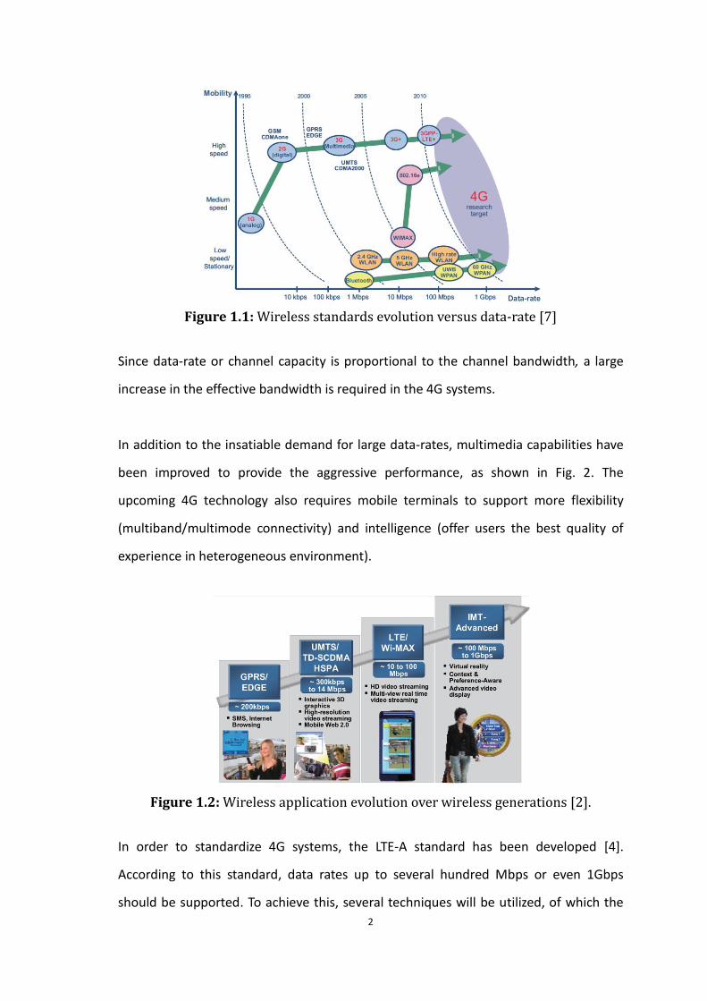
shown in Fig. 1.1, which gives us an overview of wireless standards evolution, the
data-rate has been increased from below 10 kbps (1G) to 100 Mbps (3G+), while in the
upcoming 4G systems, the data-rate is required to go up to 1 Gbps.
2
Figure 1.1: Wireless standards evolution versus data-rate [7]
Since data-rate or channel capacity is proportional to the channel bandwidth, a large
increase in the effective bandwidth is required in the 4G systems.
In addition to the insatiable demand for large data-rates, multimedia capabilities have
been improved to provide the aggressive performance, as shown in Fig. 2. The
upcoming 4G technology also requires mobile terminals to support more flexibility
(multiband/multimode connectivity) and intelligence (offer users the best quality of
experience in heterogeneous environment).
Figure 1.2: Wireless application evolution over wireless generations [2].
In order to standardize 4G systems, the LTE-A standard has been developed [4].
According to this standard, data rates up to several hundred Mbps or even 1Gbps
should be supported. To achieve this, several techniques will be utilized, of which the

3
most visible to the analog/RF part of a 4G smartphone will be the utilization of
multi-antennas and signal paths in parallel, and the use of bandwidths up to 100MHz in
each path. Therefore, we have to design a corresponding analog baseband section
which can sustain such a high bandwidth to achieve the anticipated performance.
1.2 4G Wireless standards: LTE and LTE-Advanced
Although the third-generation mobile communication system has supplied us with
much better services than 2G system has done, e.g., wider bandwidth and multimedia
service, the conflict between the ever-increasing number of mobile users and limited
bandwidth resources drives many countries and organizations to exploit the next
generation systems (4G), such as China Communication Standardization Association
(CCSA) and ITU (International Telecommunication Union). Defined by ITU’s
Radio-communication sector (ITU-R), a 4G terminal should accommodate the following
objectives [8]:
Data-rate of 1Gb/s and 100 Mb/s for stationary and high mobility
Flexible channel bandwidth from 5 MHz to 20 MHz, optionally up to 40 MHz
Smooth handoff and seamless connectivity and global roaming
High Quality of Service (QoS)
An all-IP (internet protocol) packet switched network with IP based femtocells
Interoperability with existing wireless standards
Establishing 4G systems from existing developed wireless systems is more feasible than
developing new ones. Currently, there are just two candidate technologies for 4G
systems: 3GPP LTE-Advanced and IEEE 802.16m. Industry has adopted to LTE
technology as the underpinning of 4G systems, so we will focus on the LTE technology
and its evolution LTE-A in the following section, which is the backbone of the coming
4G system.

4
1.2.1 LTE
LTE is an improvement to the current universal mobile telecommunications system
(UMTS) developed by the third generation partnership project (3GPP) [3]. It is designed
to carry high-speed data as well as support high-capacity voice traffic. It was
standardized in the form of release 8 of the 3GPP evolution. LTE is classified as a 4G
technology although it does not meet all the requirements for 4G. A variety of
techniques are utilized in the LTE systems [9]: multicarrier technology, multiple antenna
technology and packet-switched only network. We will briefly discuss the first two
techniques since they are more related to the thesis.
A. Multicarrier technology
3GPP prescribes orthogonal frequency division multiple access (OFDMA) for downlink
(DL) transmission and single-carrier frequency division multiple access (SC-FDMA) for
the uplink (UL) in order to increase the mobile terminal power efficiency, as shown in
Figure 1.3. Modulation schemes for the data transmission can be QPSK, 16QAM and
64QAM (only supported by the user category 5 for the uplink) for the uplink and
downlink [9].
(a) (b)
Figure 1.3: LTE (a) DL and (b) UL multiple access schemes (each color stands for
one user) [10].
B. Multiple antenna technology
To improve data-rate and spectral efficiency, LTE employs multiple input multiple
output (MIMO) technology. As the name suggests, more than one antenna is used in

5
the transmitter and in the receiver. One direct benefit is that multipath interference is
reduced, resulting in high data throughput. Figure 1.4 presents two applications of the
MIMO technique.
(a) (b)
Figure 1.4: MIMO system diagrams of (a) Multi-User (b) Single User [9].
In table 1.1 the key parameters of the LTE (release 8) are summarized.
Table 1.1: LTE release 8 key parameters [3] LTE release 8
Access scheme DL OFDMA
UL SC-FDMA
Scalable BW [MHz] 1.4/3/5/10/20
Modulation QPSK/16QAM/64QAM
Duplexing FDD/TDD
Spatial multiplexing
Single layer for UL
Up to 4 layers for DL
MU-MIMO support
* assume 4×4 MIMO
1.2.2 LTE-A
LTE should be considered as the pre-4G rather than 4G, since it cannot fulfill the
data-rate requirement of 4G. Table 1.2 illustrates us the data-rates and spectra
efficiency achieved by LTE and LTE-A. Clearly, LTE-A [11] can fulfill the requirements of
4G.
Table 1.2: Data-rates comparison [12] LTE LTE-A IMT-A (4G)
Peak data-rate DL 300 Mb/s 1Gb/s Stationary: 1Gb/s
high mobility: 100Mb/s UL 75 Mb/s 500 Mb/s
Spectra efficiency
[bps/Hz]
DL 15 30 15
UL 3.75 15 6.75

6
Compared with LTE, new technologies have been exploited for LTE-A [12]: carrier
aggregation (CA), enhanced multi-antenna transmission, coordinated multiple point
transmission and reception (CoMP) and relaying. We will pay attention to the carrier
aggregation technique, which is used for bandwidth extension and is closely related to
our design. For more details about the LTE-A, please refer to [13].
To achieve a 4G system’s peak data-rate target, it is necessary to extend the
transmission bandwidth used in LTE. The proposed technique is termed carrier
aggregation or channel aggregation, which means two or more contiguous or
non-contiguous carriers, can be aggregated into one transmission channel. For instance,
Fig 1.5(a) presents a transmission channel of 100MHz obtained by five contiguous
channels in LTE release 8, while Fig. 1.5(b) shows the non-contiguous approach.
(a) (b)
Figure 1.5: (a) Contiguous and (b) non-contiguous carrier aggregation [14]
1.3 Software defined radio
A software defined radio (SDR) system is defined as a radio in which some or all of the
physical layer functions are defined in software [15]. It is a reconfigurable system use a
collection of hardware and software technologies. SDR enabled devices and equipment
be dynamically programmed to reconfigure their characteristics. As a result, the
network can employ any standard, any frequency band and any channel bandwidth,
which would support conduction to the 4G era. If succeed, it would become the
dominant technology in wireless communications.

7
1.4 Design challenge and objectives
In the direct conversion (zero-IF) transceiver, the analog baseband section is
responsible for adjacent channel selectivity, anti-aliasing and dynamic range
maximization. A channel filter with low input referred noise (IRN) and high linearity is
important for the performance of the whole RF front-end. The subject of this thesis is
to design a baseband channel filter that can be used as part of a LTE-A system. It will be
required to achieve the same linearity and noise performance as is needed in
current-generation phones, but now combined with a very high bandwidth.
Design objectives in this work are: 1) design of a low pass filter with variable
bandwidth (0.7MHz~50MHz) to cover the bandwidth range of LTE-Advanced, 2) a
channel filter with high in-channel and out-of-channel linearity : at least 20 dBm at the
middle of the filter bandwidth and blockers attenuation of 10dB in the adjacent
channels), 3) a channel filter with low IRN, i.e., input noise density of 2nV/√Hz, 4) low
power consumption of a few mW, 5) small chip area (defined by maximum capacitor
value of 50pF).
However, trade-offs exist between design parameter such as linearity, noise and power
consumption [16]. The design challenge in this work is realizing the high linearity and
low IRN and low power. For instance, linearity benefits from a large overdrive voltage,
however, this would result in high power consumption.
1.5 Thesis organization
This work is a part of the research on reconfigurable radio front-ends which would be
used in SDR systems in the future. This thesis consists of 6 chapters and is organized as
follows.
In the first two sections of chapter 2, some basic theories about the zero-IF RF
front-end and analog baseband section, including the LNA, mixer and channel filter are
8
provided. Among the four different types of filters (i.e., active-RC filter, MOS-C filter,
Gm-C filter and active-R-Gm-C filter), the Gm-C filter is selected for our design due to
its advantage of high bandwidth. In the third section, we briefly review the filter design
procedure, active inductor and resistor realization techniques, and transconductance
linearization technique utilized in the Gm-C filter.
In chapter 3, two published Gm-C low pass filters are investigated. These filters are
distinguished by their working regions (voltage domain and current domain). A
dedicated section (3.2 and 3.3) is given to these two modes. Circuit simulation is done
using UMC’s 130nm technology. After analyzing each filter’s advantages and drawbacks,
the voltage mode LPF is selected due to its low noise as well as good linearity
performance. In the fourth section, different RF front-ends for the voltage-mode filter
and current-mode filter are discussed.
A tunable Gm-C filter is realized in chapter 4. According to the Gm-C filter’s feature, one
tuning algorithm is proposed in the first section. Then, according to the tuning
algorithm, a flexible transconductance Gm and capacitor array are implemented using
MOS switches in the second section. The impact of the finite on resistance of the MOS
switch on the filter performance is also discussed. Finally, to cope with low
out-of-channel linearity, a zero-IF front-end with passive mixer loaded by a tunable
capacitor is utilized to attenuate the out-of-channel blockers.
In chapter 5, the noise figure simulation results of the total receiver are presented in
the first section. Then, layout and post simulation result of the flexible filter are given,
in which the impacts of processing corners, supply voltage variation and temperature
on the filter bandwidth are discussed.
Finally, general conclusions are drawn in chapter 6. Some suggestions for improving the
filter’s performance are proposed for future work.

9
Chapter 2
Background
This chapter focuses on the theoretical background required for better understand the
following chapters. In the first section, we briefly review some basics about the zero-IF
RF front-end, analog baseband section and channel filter. Then, emphasis is put on the
Gm-C filter design, in which the filter design procedure, passive component realization,
and transconductance linearization technique are discussed.
2.1 RF front-end basics
The RF front-end plays an important role in one mobile terminal. Basics about the
zero-IF receiver, including its LNA, mixer components are reviewed in this section.
2.1.1 Zero-IF receiver
There are several architectural options available as far as receiver front-end design is
concerned, i.e., heterodyne receivers, zero-IF receivers, digital low-IF receivers,
bandpass sampling receivers and direct RF sampling receivers [16, 17]. These receivers
all have the potential to be chosen as the candidates of the SDR systems based on their
own features. However, to simultaneously achieve multi-mode and multi-standard
capabilities with cost and power savings, the zero-IF receiver wins out thanks to its
overwhelming advantage of simplicity, although several problems also exist.
Fig. 2.1 shows us the common architecture of the zero-IF receivers. In this architecture,
the received RF signal is directly translated to baseband, which is accomplished by
setting the local oscillator (LO) frequency equal to the RF signal. Therefore, no
intermediate frequency (IF) stages are needed, making this architecture quite suitable
for low power, a high level of integration as well as better flexibility to suit various
applications. In addition, there is no image rejection problem [16] as appears in

10
heterodyne receivers, which relaxes the requirements for extra filters (e.g., SAW filter),
and a low pass filter in the baseband is critical for channel selectivity.
Figure 2.1: Zero-IF receiver architecture
On the other hand, several problems exist in this topology, i.e., DC offset, even-order
distortion, I/Q mismatch, flicker noise and LO-leakage. Solutions have been developed
to cope with these problems. The DC offset problem can be alleviating by using DC-free
coding, and differential LNAs and mixers suppress the even-order distortion [16].
In conclusion, simplicity gives zero-IF receiver flexibility and the potential to reduce
power, cost and area, making it is a suitable candidate for SDR systems. However, due
to its simplicity and the flexibility requirement, more challenges are imposed on the RF
and baseband section design: high performance LNAs, high linearity mixers, flexible
channel filters and state of the art ADCs. In later chapters, we will use this architecture
as our test bench for design and simulation.
2.1.2 Receiver sensitivity and linearity
Sensitivity is defined as the minimum signal level that can be detected by the RF
front-end with acceptable signal-to-noise (SNR) ratio [16], which usually is determined
by the receiver noise figure (NF). The minimum input power can be estimated using
this equation
𝑃in,min = −174𝑑𝐵𝑚 𝐻𝑧⁄ + NF + 10logB + SNRmin, (2.1)
where B is the channel bandwidth. In a radio receiver, the noise figure is calculated
11
according to Friis’ equation (2.2)
𝑁𝐹𝑡𝑜𝑡 = NF1 +NF2−1
G1+NF3−1
G1G2+NF4−1
G1G2G3⋯, (2.2)
where NFi and Gi (i=1,2,3···) stand for the noise figure and gain of each stage
respectively. It denotes that the NF of the first stage of the receiver dominants the total
noise figure if the gain of the first stage is sufficiently large. Therefore, as the first stage
of the RF front-end, the LNA is required to have a low noise figure as well as high gain.
Receiver linearity is measured using the two-tone test in terms of input third-order
intercept point (IIP3) and denoted by
1
IIP3tot=
1
IIP31+
G1
IIP32+G1G2
IIP33+G1G2G3
IIP34⋯, (2.3)
where IIP3i and Gi (i=1,2,3···) represent each stage’s noise figure and gain, respectively.
Equation 2.3 predicts that receiver linearity is mainly determined by the stages after
the LNA due to its gain, i.e., the mixer and channel filter linearity. Therefore, a high
linearity mixer and filter are desired in the receiver.
2.1.3 LNA and mixer basics
When designing a LNA, apart from the high gain and low noise figure requirements
described above, input matching is another important specification. Theoretically,
impedance matching and noise matching are required simultaneously for maximum
power delivery and low noise. In reality, the LNA input impedance is designed so that
the input return loss (S11) is less than 10dB with an acceptable noise figure.
Linearity and noise are two main specifications when designing a mixer. An active mixer
has lower noise due to its gain; however, it suffers from lower linearity compared with
the passive mixer. In the zero-IF receiver, where flicker noise is important, the passive
mixer is popular due to its zero DC biasing current as well as its better linearity.

12
2.2 Analog baseband section basics
In the zero-IF receiver, the analog baseband section normally consists of a LPF and VGA
in series. It plays an important role in channel selectivity, anti-aliasing filtering and
dynamic range maximization. A typical baseband section permutation is illustrated in
Figure 2.2, in which signals are amplified by the VGA after its blockers are firstly filtered
by a LPF. The presence of the VGA block keeps the signal level constant no matter how
the signal changes, in order to relax the requirements (i.e., resolution, dynamic range)
on the following ADC. However, if a state-of-the-art ADC is employed, such as high
performance ΣΔ, the VGA can be removed to reduce power consumption.
Figure 2.2: Signal processing in the analog baseband section [18]
Careful design of each baseband block is required because: (1) noise figure and
linearity in the baseband circuit could deteriorate the whole performance of the
receiver, and (2) majority of the chip area and power is consumed by the baseband
components. Since the objective of this thesis is to design a flexible and high
performance LPF, we will focus on its analysis and implementation in this section.
2.2.1 Channel filter specifications
In baseband section, the input spectrum includes interferers from adjacent channels,
in-band, and out-of-band blockers in addition to the wanted signal. Usually, power level
of these interferers is much higher (around 20dBm) compared to the signal. For this
reason, the LPF should possess high in-band dynamic range (DR), out-of-band linearity

13
and anti-aliasing filtering.
In-band dynamic range of the filter is determined by its input referred noise (IRN) and
acceptable maximum input signal level. It denotes the filter’s ability of signal handling
with required SNR. In wideband systems, where thermal noise is dominant, IRN is
calculated by integrating the thermal noise in the whole band and then dividing the
result by the filter gain. With signal power increases, distortion at the filter output
becomes worse and worse. The upper limit occurs when the minimum SNR is achieved.
If an increase in dynamic range is desired, we have to lower the noise floor or increase
the filter in-channel linearity. The two-tone test to measure the filter is in-channel
linearity is shown in Fig. 2.3(a).
Excellent out-of-channel linearity is another important requirement to the channel
filter; otherwise intermodulation (IM) of two out-of-channel signals would fall into the
wanted signal band and corrupt the SNR. Sufficient attenuation of the out-of-channel
signals can lighten the burden, which usually is done by using a higher order filter. The
out-of-channel linearity measurement is shown in Fig. 2.3(b).
(a) (b)
Figure 2.3: (a) in-channel linearity and (b) out-of-channel linearity two-tone test.
Anti-aliasing filtering is illustrated in Fig. 2.4. The channel filter should have the ability
of limiting the signal bandwidth to avoid the aliasing problem caused by the folding
back of out-of-channel noise and interferers. In this figure, passband and stopband are
denoted by Fb and Fs-Fb, respectively, and Fs is the sampling frequency used in ADC.

14
When the input spectrum is limited below Fs-Fb, no aliasing into the signal band occurs.
Therefore, the channel filter should meet the desired attenuation in the stopband.
Attenuation of the blockers in transition band (between passband and stopband) is also
expected in order not to saturate the subsequent stages after amplification by VGAs.
Figure 2.4: Anti-aliasing filtering
2.2.2 Channel filter architectures
Theoretically, the active filter could be either a switched-capacitor (SC) filter or
continuous time (CT) filter depending on system requirements. In a system where high
cut-off frequency filters are required, the CT filter is superior to the SC filter which has
to use two high frequency non-overlap clock signals, and would consume too much
power [19]. Therefore in our wideband system, we focus mainly on the implementation
of CT filters.
Fig. 2.5 presents four configurations of continuous time filters [20]. From the linearity
point of view, (a), (b) and (d) offer higher linearity owing to their closed feedback loop
structures compared to the open loop structure (c). However, this advantage does not
exist anymore at high frequency due to the decrease of loop gain. From the tuning
accuracy perspective, topology (b) is the simplest one since it can be tuned by changing
the control voltage Vb, instead of using resistor or capacitor banks or extra tuning
circuits as in other three topologies. However, if filters with high frequency and low
power consumption are desired, as is the case of the SDR, topology (c) would be the

15
best choice if linearization techniques also can be used.
(a) (b)
(c) (d)
Figure 2.5: Four types of continuous time active filter (a) active-RC filter (b)
MOS-C filter (c) gm-C filter (d) active gm-RC filter
To sum up, the gm-C filter is the best candidate for channel filtering although its
linearity is not good enough. Low power consumption and wide bandwidth are its main
advantages compared to other types of filters. That is why designing a gm-C filter is the
objective of this thesis.
2.3 Gm-C low-pass filter design basics
In this section, filter design basics of filter design methodology, passive component
realization and Gm linearization techniques are briefly discussed.
2.3.1 Filter design methodology
As described in [18], there are a few steps utilized to design a filter: filter mask
estimation, filter type selection and filter parameter determination.

16
In the presence of the adjacent channels, the channel filter should have the ability to
pick up the signal from the assigned channel with high accuracy. The system adjacent
channel selectivity (ACS) specification defines the minimum attenuation demanded at
the frequency offset from the assigned channel, thereby defining the filter mask.
However, ACS is usually achieved by the analog filter (channel filter) and digital filter
together, and the selectivity for the analog filter is assigned given the filter power and
ADC performance.
Having known the filter mask, we define a polynomial approximation whose frequency
response fits the mask curve precisely. Generally, there are four types of filters, i.e.,
Butterworth, Chebeyshev, Bessel and Elliptic, and each type has its own advantages
and drawbacks. The most suitable filter is selected according to the system
specifications. For instance, a Bessel filter is the best candidate if good phase response
is demanded, while Butterworth filter is used for in-channel maximum magnitude
flatness in the frequency domain [21, 22].
With the filter mask and the selected filter, the filter parameters such as the order, gain,
and cutoff frequency can be determined easily.
2.3.2 Passive component realization
In a typical Gm-C filter, passive components such as the resistor and inductor are barely
used. Usually, we can implement them with the assistance of a Gm cell. As can be seen
in Fig. 2.6 (a), it is easy to obtain one active resistor of 1/gm when connecting the
output node to the minus input node of the gm cell, as is the case of diode connected
MOS transistor. Therefore, we put the emphasis on the active inductor realization.
The on-chip inductor is avoided in integrated circuits nowadays due to its drawbacks
such as large chip area consuming and low quality factor. Thus, the active inductor
approach has been developed to realize an inductor. The active inductor usually is
17
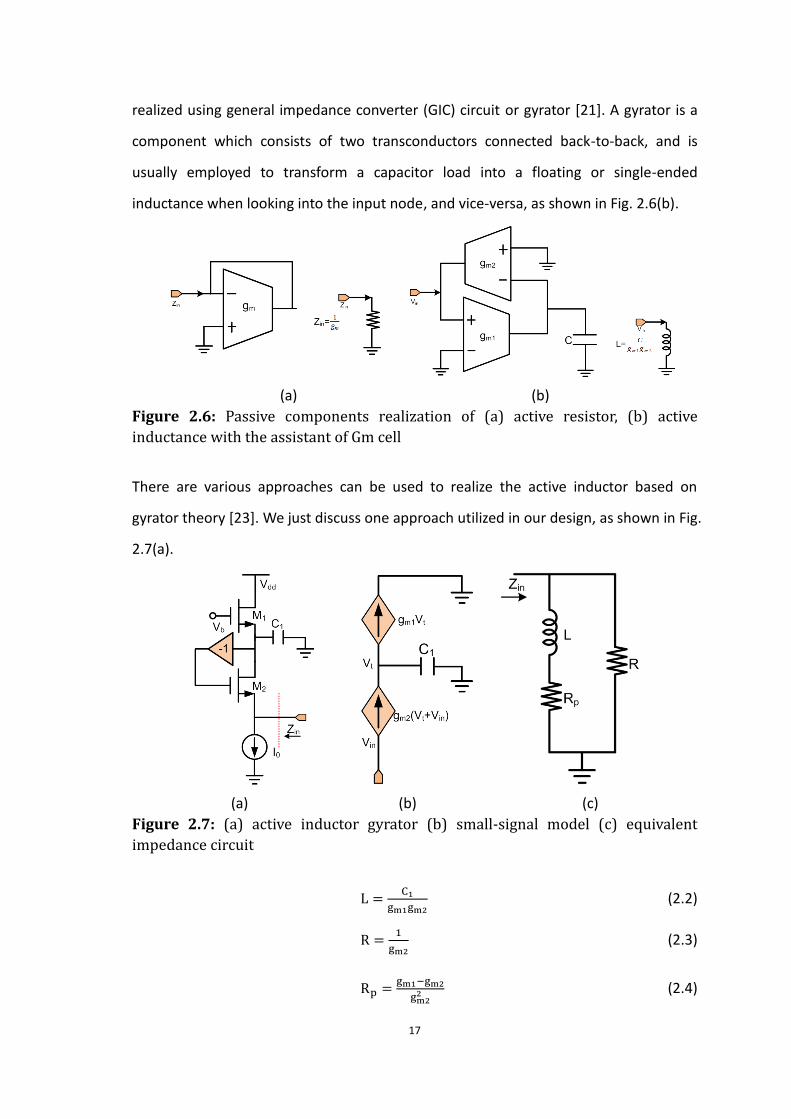
realized using general impedance converter (GIC) circuit or gyrator [21]. A gyrator is a
component which consists of two transconductors connected back-to-back, and is
usually employed to transform a capacitor load into a floating or single-ended
inductance when looking into the input node, and vice-versa, as shown in Fig. 2.6(b).
(a) (b)
Figure 2.6: Passive components realization of (a) active resistor, (b) active
inductance with the assistant of Gm cell
There are various approaches can be used to realize the active inductor based on
gyrator theory [23]. We just discuss one approach utilized in our design, as shown in Fig.
2.7(a).
(a) (b) (c)
Figure 2.7: (a) active inductor gyrator (b) small-signal model (c) equivalent
impedance circuit
L =C1
gm1gm2 (2.2)
R =1
gm2 (2.3)
Rp =gm1−gm2
gm22 (2.4)

18
According to the small signal model of Fig. 2.7(b), we can calculate the equivalent input
impedance versus frequency. Each value of the components in Fig. 2.7(c) is given in
equations (2.2-2.4). With equal gm in the two transistors, a parallel equivalent circuit
analyzing of inductor L=C1/g2m with resistor R=1/gm is realized. Note that the minus
sign can be realized by a cross-coupled differential pair.
2.3.3 Gm linearization techniques
A differential pair is the simplest transconductor, whose distortion comes from the
odd-terms due to its odd-symmetric transfer function. Under the small input signal
condition, third order distortion HD3 dominants given by (2.5)
HD3 =Vin2
32(VGS−VTH)2 , (2.5)
where Vin is the differential input signal amplitude. Therefore, one way to improve the
linearity is to increase the overdrive voltage Vov (Vov=VGS-VTH) of the differential pair.
However, this approach is not popular due to higher power consumption and limited
linearity improvement. Several approaches [19, 24] have been developed to improve
the linearity of the transconductance Gm.
Local feedback is one popular technique to achieve better linearity. One practical
circuit is shown in Fig. 2.8 with source degeneration resistor. The third order harmonic
is suppressed due to gm linearization
HD3′ =
HD3
(1+gmRs)2 (2.6)
gm′ =
gm
1+gmRs, (2.7)
where Rs is the degeneration resistor. However, the disadvantage is the parasitic
capacitance of the current source may degrade the filter’s performance at high
frequency. Moreover, noise is introduced by the degeneration resistor. In order to make
a tunable transconductor, the resistor can be replaced with MOS transistor working in
the linear region.

19
Figure 2.8: Source degeneration technique for gm linearization
Parallel differential pair technique is another one effective way of improving linearity,
as shown in Fig. 2.9. Theory behind is that this circuit has a slower slope in I/V curve
than that of the single differential pair. Best results (reduced distortion and extent
input range) are achieved when the transistor ratio in one pair is 5:1 [24]. However,
good performance is achieved at the expensive of transconductance. Moreover, power
consumption is higher compared with the single differential pair.
Figure 2.9: Parallel differential pair for gm linearization
Apart from the linearization techniques mentioned above, there are some other
attractive ways which take the advantages of the inherent linear behavior of the
invertor or the biased in the linear region differential pair. The Nauta transconductor
shown in Fig. 2.10 is such a circuit employing the invertors. High frequency behavior is
the main advantages since there are no internal nodes. In addition, it is suitable for low
supply voltage application. However, common mode feedback circuit is desired.

20
Figure 2.10: The Nauta transconductor
2.4 Summary
In this chapter, we briefly reviewed the theory background about the zero-IF receiver
front-end and the analog baseband section, including their sub-blocks such as LNA,
mixer and channel filter. Then, based on the Gm-C type filter, we discussed the filter
design procedure, passive components realization and the transconductance
linearization techniques. In the following chapters, our objective is to design and test a
Gm-C filter based on this discussion.

21
Chapter 3
Gm-C Biquad Design and Simulation
Results
A biquad, defined as one circuit who can realize the biquadratic transfer function, is
very useful because higher order filter systems may be realized by simply cascading
them [21]. Therefore, our objective in this chapter is to investigate the way of designing
a simple biquad with good performance, i.e., in-channel linearity of 20dBm, power
consumption of a few mW, input referred noise density of 2nV/√Hz, and dynamic range
of at least 60dB.
This chapter starts with the analysis of two published Gm-C biquads based on the RLC
networks, which can be classified into voltage mode and current mode. In the following
two sections, we discuss the advantages and drawbacks for each type, and simulations
are done in the UMC 130nm technology. Then, different zero-IF structures for these
two filters are presented. Conclusions are drawn in the last section.
3.1 Two Gm-C biquads
As described in last chapter, the classical Gm-C filter suffers from low linearity due to its
open loop structure. Therefore, efforts have been made to improve the linearity of the
transconductance [27-29]. However, these posted structures either consume high
power (several mW) or require high supply voltage (greater than 1.8V), which prevents
them from use in a low power application such as the LTE-A system. In this section, we
discuss two novel structures published in [30-31], as shown in Fig. 3.1.

22
(a) (b)
Figure 3.1: Two types of biquads (a) voltage mode [30], (b) current mode [31]
classified by their working regions.
Fig. 3.2 presents Thevenin equivalent circuits corresponding to each circuit in Fig. 3.1.
Clearly, the voltage-mode biquad is actually based on the series RLC network while the
current-mode biquad is from the parallel RLC network model. The active inductor L is
realized by way of GIC approach described in chapter 2. We will analyze these two
biquads with their advantages and drawbacks in the following sections.
(a) (b)
Figure 3.2: Thevenin equivalent circuits of (a) voltage-mode biquad, (b)
current-mode biquad
3.2 Voltage-mode Gm-C filter
As can be seen from Fig. 3.1(a), the voltage-mode Gm-C biquad is based on the source
follower (i.e., M1 and M3). We will investigate the first-order filter before the biquad,
in order to see what benefits we can obtain from the source-follower based structure.

23
3.2.1 Source-follower based first-order filter
(a) (b) (c)
Figure 3.3: Source-follower based LPF (a) schematic (b) small-signal model (c)
loop gain model.
Fig. 3.3 presents the source-follower based first-order low-pass filter with its
small-signal models shown in Fig. 3.3(b) and (c). The latter one is used to calculate the
loop gain of the source follower.
A. Transfer function
Taking the body effect (gmb) and the channel length modulation effect (gds) into account,
the transfer function of this first-order filter is given in (3.1),
H(s) =gm
sC+gm+gmb+gds+gds0 . (3.1)
where gds0 is the output conductance of the current source I0. The filter’s poleω0 and
DC-gain KDC are
𝜔0 =gm+gmb+gds+gds0
C (3.2)
𝐾𝐷𝐶 =gm
gm+gmb+gds+gds0. (3.3)
Equation (3.3) shows that the filter gain is always less than 1, even if the body effect
and channel modulation effect are negligible, equation (3.2) reveals that gmb, gds and
gds0 together shift the filter pole away from the designed value. Therefore, triple well
technology (to cancel the body effect gmb) and longer channel length (to lower gds since
gds∝1/L) are expected.
B. Linearity consideration
A source follower is relatively linear thanks to its intrinsic feedback loop formed by M1

24
and its load impedance Zs. According to Fig. 3.3(c), the loop gain LG is written as
𝐿𝐺 =gm
(sC+gmb+gds+gds0). (3.4)
In a differential circuit where HD3 is dominant, HD3 can be suppressed by a factor equal
to the loop gain LG:
𝐻𝐷3,𝑆𝐹 =HD3
(1+𝐿𝐺)2. (3.5)
Besides, given the same gm, compared with other Gm-C filters which get high linearity
by increasing the overdrive voltage, the source follower based filter requires a low
overdrive voltage (Vgs-Vth) thus consumes less power according to (3.6):
gm =2I0
Vgs−Vth . (3.6)
Low power consumption with high linearity is the main advantage of this filter.
Body effect (gmb) plays an important role in this source follower based filter [24]. In our
above calculations, we assume the gmb is linear and can be treated as one conductance.
This is true when the amplitude of Vbs is small and has a negligible impact on the
threshold voltage, Vth. However, in the large signal case, this filter shows severe
distortion problem due to the nonlinearity of gmb.
In addition, from (3.4) we can see that LG has one pole at low frequencyωp
𝜔𝑝 =gmb+gds+gds0
C (3.7)
compared with (3.2), which means LG decreases in the filter bandwidth. Consequently,
filter linearity decreases with increasing filter bandwidth, which is one drawback of this
filter.
C. Noise
The output noise contributed by the transistor M1 and current source I0 is calculated as
Vout,n2 = 4kTγ(gm + gm0) |
1
sC+gm+gmb+gds+gds0|2 , (3.8)
where k is the Boltzmann constant and T is the absolute temperature, γ is the transistor

25
channel thermal noise factor. According to (3.8), the output noise has the same pole as
of the transfer function. In order to decrease the output noise, we have to make the
current source transconductance gm0 as small as possible. Meanwhile, high gm is
desired.
From the above analysis we can get a conclusion: the main advantage of the
source-follower based filter is its high linearity with low power consumption, which
makes this filter very suitable for the channel filter in the baseband.
3.2.2 Source-follower based biquad filter
(a) (b)
Figure 3.4: Source-follower based biquad (a) filter circuit, (b) its half circuit
small-signal model
As a matter of convenience, we redraw the source-follower based biquad here as well
as its small-signal model in Fig. 3.4 (b). Analysis in detail is given next.
A. Filter parameters
According to the small signal model Fig. 3.3(b), we can calculate the transfer function
assuming gds is negligible compared with gm. The transfer function H(s), quality factor Q
and the cutoff frequency ω0 are given by equations (3.9)-(3.11). In the case of equal gm,
Q is simply determined by the ratio of C2 to C1.
H(s) =−1
s2C1C2
gm1gm2+s(
C1−C2gm1
+C2gm2
)+1
gm1=gm2⇒
−1
s2C1C2gm2 +s
C1gm+1
(3.9)

26
Q =1
√gm2gm1
(√C1C2−√
C2C1)+√
gm1gm2
√C2C1
gm1=gm2⇒ √
C2
C1 (3.10)
ω0 = √gm1gm2
C1C2
gm1=gm2⇒
gm
√C1C2 (3.11)
Note from (3.9), the DC gain is ideally -1. When taking into account the finite output
conductance and body effect, the filter will suffer from a few dB loss. The loss can be
estimated according to
𝐾𝐷𝐶 = (gm
gm+gmb+gds+gds0)2 . (3.12)
B. Noise performance
There are 6 noise sources in total in the voltage-mode biquad as shown in Figure 3.5.
When referred them to the input node, we can obtain the input-referred noise (IRN).
(a) (b)
Figure 3.5: (a) noise sources of the biquad and (b) its equivalent input noise.
Equation (3.13) indicates us the total IRN and the responding each contributor (labeled
by names) of the biquad.
IRN2 = 8kTγ [1
gm⏟M1,3
+1
gm|1 + j
f
Qf0|2
⏟ M2,4
+gm0
gm2 |j
f
Qf0|2
⏟ I0
] , (3.13)
where Q and f0 are the quality factor and cutoff frequency, respectively. Flicker noise is
omitted here because it is assumed that a large transistor is used. It is obvious from
(3.13) that the noise introduced by the current sources I0 is shaped by high pass

27
transfer function as well as M2,4. Given certain values of bandwidth f0 and quality factor
Q and assuming that gm0 equals gm , we can plot the IRN in different gm as shown in Fig.
3.6.
Figure 3.6: Input noise value (integrated from 100 kHz to 50 MHz) versus gm
when Q=0.71 and f0=50MHz.
According to Fig. 3.6, larger transconductance gm leads to smaller IRN which is what we
expect. However, we cannot increase gm too much, since according to (3.11) gm is
proportional to the square value of the capacitor product. Therefore a large gm
demands a large capacitor, and a trade-off exists between noise and the filter area
on-chip.
C. Linearity performance
This filter biquad has good linearity for the following reasons: (1) differential structure
cancels out the even-order harmonics and HD3 is dominant, (2) the intrinsic negative
feedback loop of the source follower can suppress harmonics at low frequency, (3) this
filter merely operates in the voltage domain and there are no V/I or I/V conversions.
However, when the frequency approaches the cut-off frequency, the linearity drops
because of the decrease in the loop gain.
A longer channel length is beneficial to the linearity because distortion can also result
from transistor conductance variation. However, it cannot be arbitrary large due to the
parasitic capacitance of a large area transistor.
D. Stability

28
Care should be taken of the stability problem due to the positive feedback formed by
the cross-coupled differential pair. Breaking the loop at the gates of M2 and M4, we
can get the loop gain shown in equation (3.14),
LP =
gds0gm
+s∙Q
ω0s2
ω02+s∙
Q+1/Q
ω0+1
, (3.14)
where gds0 is the current source transconductance. Clearly, it shows a band pass
response. Simulation results will be given in following section to check the stability.
E. Filter supply voltage requirement
The minimum supply voltage is estimated in this section. According to Fig. 3.7,
assume that the current source has the same overdrive voltage (Vov) as transistors
M1-M4 and the signal amplitude (differential zero to peak) is Vswing. The minimum
required supply voltage is,
Vdd,min = 2Vov + Vgs + Vswing = 3Vov + Vth + Vswing. (3.15)
Figure 3.7: Supply voltage estimation
Note that in this structure, the maximum voltage swing (Vswing) is limited by the
threshold voltage of M2 and M4 since large Vswing will drive these transistors into triode
region.
F. Power consumption
As mentioned in last section, low power consumption is considered to be the main
advantage of this biquad cell because we can bias the transistors at low overdrive

29
voltage. In addition, no common mode feedback (CMFB) circuit is required, since the
output biasing point is fixed by the gate-source voltage and the input DC point.
Therefore, there is no power budget for a CMFB circuit. Finally, there are no passive
resistors, since in this biquad no DC power is dissipated. In total, the power
consumption is 2I0*VDD.
3.2.3 Voltage-mode biquad design procedure and simulation results
In this section, a design example of the voltage-mode biquad filter is presented as well
as the simulation results. The technology library used is the 130nm UMC technology
with a supply voltage of 1.2 V.
A). Channel length (L) selection
With the scaling of CMOS technology, transistor can handle faster and faster signals
due to the short channel length. At the minimum channel length in 130nm technology,
the cutoff frequency fT can go up to 100GHz. In the zero-IF baseband section, however,
such frequency is not needed. Therefore, we can use longer channel length transistors
in the baseband. In addition, as mentioned above, a long channel transistor is desired
to reduce the channel modulation effect. From the matching perspective, the long
channel length transistor has a better matching property which is beneficial to filter’s
sensitivity. Fig. 3.8 shows fT of the PMOS and NMOS at different Vgs and L. channel
length for M1-M4 is fixed at L=500nm. As for the current sources I0, L=1um is used.
Figure 3.8: NMOS and PMOS cutoff frequency versus Vgs at different channel
length L: Red line for L=500nm and blue line for L=800n.

30
B). Selecting the gm value
As mentioned in Chapter one, the LTE mobile communication system employs a
multi-antenna transceiver architecture with zero-IF I/Q detection. Thus, there are at
least two receiver paths. In the baseband section, there would be at least four variable
bandwidth filters. The filter size, mainly occupied by the capacitors, becomes a critical
problem in the LTE system. In order to confine the baseband section into a reasonable
chip area, we expect each capacitor to be reasonable small. According to equations
(3.10-3.11), a small gm value indicates small capacitor area given certain a Q. On the
other hand, according to Fig. 3.6, gm determines the input noise value given a certain
quality factor Q and cutoff frequency f0. A large gm is expected to result in a IRN as
small as possible. Therefore, a tradeoff exists between the chip area and IRN.
In the end, gm= 5mS is selected since in this case C is around 10pF and the IRN is
acceptable (i.e., a Vswing of 300mV gives a dynamic range of 67dB). In the following part,
NMOS biquads with Q=0.71 and gm=5mS is used in our design.
C). Biasing condition
For the NMOS at L=500nm, threshold voltage Vthn varies between 0.27V~0.34V when
source bulk votalge Vsb changes between 0 and 0.7V. With the supply voltage of 1.2V,
high overdrive voltage might does not work according to equation (3.15). Since low
overdrive voltage is beneficial to the filter linearity based on our previous analysis, in
this circuit, M1~M4 are biased at around 100mV. As for the current sources, 120mV is
used.
D). Stability
Figure 3.9: Loop gain simulation

31
According to equation (3.14), loop gain of the biquad cell shows band pass response.
This agrees very well with the simulation result (Fig. 3.9). As can be seen from the
curve, the loop gain peaks at 50MHz with 0.33. Therefore, the loop gain is always less
than one and stability is guaranteed.
E). AC response
According to equation (3.12), the estimated biquad DC gain of -1.6dB (gmb=0.5mS in
this case) is obtained when neglecting gds. This value agrees with the simulation result
(-1.97dB) shown in Fig. 3.10. The graph also shows that beyond the cutoff frequency of
50MHz the roll-off is around -20dB/dec, which is expected for the all-pole second-order
filter. Finally, this filter does not suffer from the parasitic zero since it is at a very high
frequency (higher than 5GHz).
Figure 3.10: Biquad gain simulation (|H(s)|)
F). Input referred noise (IRN)
Figure 3.11: Input referred noise (IRN) simulation

32
Fig. 3.11 presents the noise performance of the biquad. According to the curve, the
minimum input referred noise density is about 3.4nV/√Hz at 10MHz, mainly from
thermal noise. At low frequency, flicker noise is dominant and the flicker corner
frequency (intersection point between flicker noise and thermal noise [16]) is around
10 kHz. When the frequency approaches and exceeds the cutoff frequency, the noise
density rises up, as predicted by equation (3.13). After Integrating from 100 kHz to
50MHz, we can obtain the total input equivalent noise of 29.14μV, which is in
accordance with the value calculated according to Fig. 3.6.
G). In-channel linearity
In-channel linearity (IIP3) is simulated through the two-tone test with a tone spacing of
1MHz. The simulation result of IIP3 versus frequency is shown in Fig. 3.12. Clearly, IIP3
becomes worse and worse as the frequency increases, which is predicted by our
previous analysis (loop gain of the source follower decreases with increasing
frequency). At the cutoff frequency of 50MHz, the IIP3 is degraded to around 3dBm.
The degradation of in-channel linearity versus frequency is the main defect of this filter.
Figure 3.12: IIP3 vs. the center frequency of the two-tone test with frequency
space of 1MHz
H). Out-of-channel linearity

33
Figure 3.13: Out-of-channel linearity two-tone test with one frequency at 100MHz
and the other at 190MHz. Input signal power used for simulation is -15dBm, and
the output spectrum power is shown on the right y-axis.
Fig. 3.13 shows the two-tone simulation result in out-of-channel linearity. The third
order IM product falls into the filter passband at 10MHz. according to Fig. 3.13 and the
calculated out-of-linearity is around 3dBm. This biquad is not a good filter for the LTE
communication system as it cannot reject the strong out-of-channel blockers.
I). Dynamic range
Figure 3.14: THD simulation with input signal frequency of 10MHz.
According to Fig. 3.14 (at 10MHz), the total harmonic distortion (THD) of -40dB is
obtained when the input signal swing is about 340mVpeak. Given the input noise of
29.14μV, the dynamic range of the filter is 78.3 dB at this frequency.
To sum up, we list all the filter parameters in the tables 3.1 and 3.2. Table 3.1 shows

34
the filter general information, and table 3.2 presents the filter performance. As can be
seen from these tables, the voltage-mode filter has a dynamic range of 78.3dB with
power consumption of 0.847mW. However, the in-channel linearity degrades with
increasing frequency; moreover, the out-of-channel linearity is very poor.
Table 3.1: Voltage-mode biquad filter parameters
gm
[mS]
gmb
[mS]
overdrive
voltage[mV]
W/L
[μm]
I0
[μA]
Cap
[pF]
M1,3 5 0.4 94 54.4/0.5
353 C1/2=11.25
C2/2=5.625 M2,4 5 0.5 94 55.04/0.5
I0 4.35 -- 124 79.36/1
Table 3.2: Voltage-mode filter performance
Power consumption [mW] 0.847
DC gain [dB] -1.967
IRN [μV] 29.14
IIP3 from DC to 50MHz [dBm] ∆f=1MHz 24.7-3.12
Out-of-channel IIP3 [dBm]
@100, 190MHz 3
Differential Input signal Vdd,zp
@THD=-40 dBc [mV]
340
Dynamic Range [dB] 78.3
3.3 Current-mode filter
As shown in Fig. 3.2(b), the equivalent circuit of Fig. 3.1(b) is a paralleled RLC network
which works in current domain. This current mode filter actually is based on the
common-gate stage, and can be utilized at the output stage of current mixer. In this
section, the first-order common-gate filter will be discussed first, and then we turn to
its biquad schematic.
3.3.1 Common gate based first order filter
The common gate stage, known as the current buffer due to its unity current gain, can
also be employed for the filter just like the source follower. A first-order filter is shown
in Fig. 3.15.

35
Figure 3.15: Current-mode first-order LPF with its small-signal model
A. Transfer function
Neglecting the transistor output conductance and body effect, the transfer function is
written as (3.16) taking into account the current source impedance Rs.
H(s) =𝑖out
𝑖in=
gm
sC+gm+1 Rs⁄ (3.16)
The filter poleω0 and DC gain KDC are
𝜔0 =gm+1/Rs
C (3.17)
𝐾𝐷𝐶 =gm
gm+1/Rs (3.18)
From equations (3.17-3.18), the source impedance Rs affects the filter pole frequency
and DC-gain.
B. Linearity consideration
In general, for one MOS transistor, drain current is expressed by (3.19) [32]
id = f(vgs, vds, vbs) (3.19)
vds and vbs influence the drain current to some degree through gds and gmb. In order to
reduce the distortion resulting from vds, a longer channel length transistor is always
desired. Besides, due to each internal node is low impedance, i.e., node A in Fig. 3.6,
common-gate stage shows little distortion since voltage variation at node A is very
small. And better linearity is obtained if we use a larger source impedance Rs.
C. Noise consideration

36
The main advantage of this current-mode filter is its noise shaping feature, as shown in
Fig. 3.16. At low frequency, the noise current of M1 re-circulates in itself (red arrow in
Fig. 3.16(a)), thus contributes nothing to the output current, while most of the noise
current of I0 goes to the output.
(a) (b)
Figure 3.16: Output noise contributed by each of the noise sources at (a) low
frequency, (b) high frequency
Above the pole frequency, the noise current of M1 flows out of the output node, but
noise produced by I0 is shorted by the capacitance C1 to ground. Therefore, the noise
current of M1 shows a high pass transfer function, which means in-band noise of M1 is
pushed out of the filter bandwidth. And noise produced by I0 follows the same transfer
function as the signal. As for the noise source of I1, since it appears directly at the
output, an ultra-low gm,I1 is necessary to decrease the noise.
In conclusion, the main merit of this common-gate filter is its noise shaping feature if
the noise contributed by the current sources are negligible.
3.3.2 Common-gate based biquad filter
In this part, we consider the low pass biquad filter based on the common gate shown
in Fig. 3.17 with respect to filter parameters, noise, linearity and power consumption.
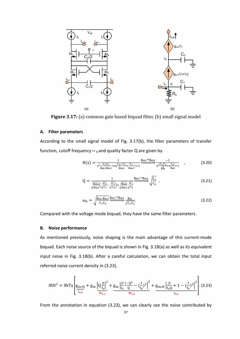
37
(a) (b)
Figure 3.17: (a) common gate based biquad filter, (b) small signal model
A. Filter parameters
According to the small signal model of Fig. 3.17(b), the filter parameters of transfer
function, cutoff frequencyω0 and quality factor Q are given by
H(s) =1
s2C1C2
gm1gm2+s(
C2−C1gm2
+C1gm1
)+1
gm1=gm2⇒
−1
s2C1C2gm2 +s
C2gm+1
, (3.20)
Q =1
√gm1gm2
(√C2C1−√
C1C2)+√
gm2gm1
√C1C2
gm1=gm2⇒ √
C1
C2 , (3.21)
ω0 = √gm1gm2
C1C2
gm1=gm2⇒
gm
√C1C2. (3.22)
Compared with the voltage mode biquad, they have the same filter parameters.
B. Noise performance
As mentioned previously, noise shaping is the main advantage of this current-mode
biquad. Each noise source of the biquad is shown in Fig. 3.18(a) as well as its equivalent
input noise in Fig. 3.18(b). After a careful calculation, we can obtain the total input
referred noise current density in (3.23).
IRN2 = 8kTγ [gm,I0⏟I0,b
+ gm |Qjf
f0|2
⏟ M1,3
+ gm |jf
f0
1−Q2
Q− (
f
f0)2|
2
⏟ M2,4
+ gm,I0 |jf
f0Q+ 1 − (
f
f0)2|
2
⏟ I0,u
]. (3.23)
From the annotation in equation (3.23), we can clearly see the noise contributed by

38
each transistor in the biquad.
Figure 3.18: (a) noise sources of the biquad and (b) its equivalent input noise.
As expected, the noise behavior of M1,3 and M2,4 shows a frequency dependent
property. In order to decrease the noise associated with the current sources, we should
make sure that the transconductance gm,I0 is very small according to equation (3.23).
Assume gm,I0 is one-half of gm, the integrated value of IRN (from 100KHz to 50MHz)
versus gm is shown in Fig. 3.19 (red curve). The blue curve in Fig. 3.19 is the noise
associated with the current sources. Clearly, current sources are the main noise
sources in this filter if gm,I0 is comparable with gm.
Figure 3.19: Integrated input noise value (from 100kHz to 50MHz) versus gm at
Q=0.71, f0=50MHz and gm, I0=gm/2
C. Linearity performance
Linearity is checked through the input impedance of this biquad (Fig. 3.17), as

39
described by equation (3.24);
Zin(s) =sC2gm2
s2
ω02+
s
ω0Q+1
. (3.24)
Inserting the values of gm=5mS, Q=0.71 and f0=50MHz, we can get the simulation result
shown in Fig. 3.20.
Figure 3.20: Current-mode filter input impedance versus frequency at gm=5mS,
Q=0.71 and f0=50MHz.
According to the graph, high linearity can be achieved at low frequency due to the low
input impedance. However, when the frequency goes up the input impedance also
increases and peaks at the cutoff frequency. Therefore, the in-channel linearity of the
current-mode filter will decrease as the frequency approaches f0, as in the case of
voltage-mode filter. After exceeding f0, the impedance reduces, thus high linearity is
obtained outside of the filter bandwidth.
D. Minimum supply voltage estimation
One advantage of current-mode circuit over its voltage-mode counterpart is the former
one can provide the opportunity for low power supply application, since voltage swing
at each internal node is small. The biquad minimum supply voltage can be estimated
according to Fig. 3.21,

40
Figure 3.21: Current mode biquad supply voltage estimation
in which Vov is the overdrive voltage of M1-M4, Vth is the transistor threshold voltage
and X is the voltage margin for the internal nodes. The required supply voltage can be
written as:
Vdd,min = 2Vov,I0 + Vgs + Vov + X = 2Vov,I0 + 2Vov + Vth + X (3.25)
Note that In order to reduce the current source noise, we have to make sure Vov,I0 is as
large as possible. Therefore, the minimum required supply voltage is determined from
the noise considerations.
E. Power consumption
As with the voltage-mode filter, this filter also has the advantage of low power
consumption. If noise is not the first consideration, the power consumption can be
reduced further.
3.3.3 Current-mode biquad design procedure and simulation results
The current-mode filter design procedure is similar to that of the voltage-mode filter.
Thus, we will put the emphasis on the current-mode filter performance merits of gain,
noise linearity and dynamic range for brevity.
A). Gain simulation
The small-signal frequency response of the current mode filter is shown in Fig. 3.22.
The DC gain is -0.37dB. At high frequency, this filter has a roll-off of 40dB/dec, as

41
expected.
Figure 3.22: Current mode biquad filter gain simulation
B). Input-referred noise
Fig. 3.23 (a) presents the IRN simulation result with a minimum noise current density
of 5.93pA at 7MHz. After integration from 100 kHz to 50MHz, the input-referred noise
is 50.03nA.
Figure 3.23: Current-mode biquad noise simulation of (a) IRN density, (b)
proportion of spot noise at 7MHz.
The pie chart shown in Fig. 3.23(b) shows that at 7MHz, the noise contributed by
current sources is 86% of the total noise, which is consistent with Fig. 3.19.
C). In-channel linearity

42
Figure 3.24: Current-mode biquad channel IIP3 versus frequency (two-tone test
with spacing of 1 MHz). Note that IIP3 is expressed in the form of input current
amplitude (zero-to-peak) in mAp.
In-channel linearity of the current mode filter is plotted in Fig. 3.24. According to this
graph, in-channel linearity decreases from 6.1mAp to 0.96mAp with increasing
frequency, as pointed out previously.
D). Out-of-channel linearity
Figure 3.25: Current-mode biquad out-of-channel linearity two-tone test with one
frequency at 100MHz and the other at 190MHz. Input signal power is -16dBm.
Note that the presence of the others spurs is due to the beat frequency used in our
simulation.
Filter out-of-channel linearity is measured by two-tone test with one frequency at
100MHz and the other at 190MHz (the beat frequency used is 10MHz). The third-order
IM product falls in band at 10MHz. According to the output spectrum shown in Fig.
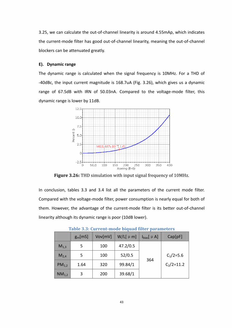
43
3.25, we can calculate the out-of-channel linearity is around 4.55mAp, which indicates
the current-mode filter has good out-of-channel linearity, meaning the out-of-channel
blockers can be attenuated greatly.
E). Dynamic range
The dynamic range is calculated when the signal frequency is 10MHz. For a THD of
-40dBc, the input current magnitude is 168.7uA (Fig. 3.26), which gives us a dynamic
range of 67.5dB with IRN of 50.03nA. Compared to the voltage-mode filter, this
dynamic range is lower by 11dB.
Figure 3.26: THD simulation with input signal frequency of 10MHz.
In conclusion, tables 3.3 and 3.4 list all the parameters of the current mode filter.
Compared with the voltage-mode filter, power consumption is nearly equal for both of
them. However, the advantage of the current-mode filter is its better out-of-channel
linearity although its dynamic range is poor (10dB lower).
Table 3.3: Current-mode biquad filter parameters
gm[mS] Vov[mV] W/L[μm] Ibias[μA] Cap[pF]
M1,3 5 100 47.2/0.5
364 C1/2=5.6
C2/2=11.2
M2,4 5 100 52/0.5
PM1,2 1.64 320 99.84/1
NM1,2 3 200 39.68/1

44
Table 3.4: Current-mode filter performance
Power consumption [mW] 0.874
DC gain [dB] -0.37
IRN [nA] 50.03
IIP3 from DC to 50MHz [mAp] ∆f=1MHz 6.11-0.96
Out-of-channel linearity [mAp]
@100, 190MHz 4.55
Add,zp @THD=-40 dBc [μA] 168.7
Dynamic Range [dB] 68.5
3.4 RF front-ends for voltage-mode and current-mode filters
There are two different receiver structures for each filter, as shown in Fig. 3.27. In
these two structures a passive mixer core is used as an example. In Fig. 3.27(a), since
the input impedance of the filter is capacitive, voltage is the mixer output (no current
flows into the filter at baseband frequency). While in Fig. 3.27(b), due to the low input
impedance of the current-mode filter, the mixer output current drives the filter. Note
that two AC coupling capacitors are used in Fig. 3.27(b) to block the DC current flowing
through the mixer.
(a) (b)
Figure 3.27: RF front-ends for (a) voltage-mode filter (b) current-mode filter.

45
3.5 Conclusion and Summary
To sum up, we list the advantages and disadvantages of the both filters in table 3.5. By
comparing these two filters, we can see they dissipate almost the same power.
However, with 1.2V as the supply voltage, the current-mode filter is less attractive due
to the noise problem resulting from the bias current sources. Moreover, its dynamic
range is smaller by 10dB. Although it has good out-of-channel linearity, we have
decided to use the voltage-mode filter in our following design. Therefore, Fig. 3.27(a)
will be the test bench for our further simulations.
Table 3.5: Comparison between the voltage-mode and current-mode filters
Advantages Disadvantages
Voltage-mode
filter
(1) Dynamic range: 78.3dB
(2) Power consumption:0.847mW
(1) Poor out-of-channel linearity
(2) In-channel linearity decreases
with increasing frequency
Current-mode
filter
(1) Good out-of-channel linearity
(2) Power consumption:0.874mW
(1) Dynamic range: 68.5dB
(2) In-channel linearity decreases
with increasing frequency
(3) Current source noise is critical
(1.2V supply voltage)
In this chapter, we analyzed and simulated two different Gm-C biquads distinguished by
their working domains: a voltage-mode filter and a current-mode filter. Simulations
were carried out in 130nm UMC technology. According to the analysis and simulation
results, each of them has its own advantages and disadvantages. For instance, the
voltage-mode filter has higher dynamic range while it suffers from poorer
out-of-channel linearity than the current-mode filter. However, the in-channel linearity
for both of them drops with increasing frequency. By comparing their performance
with respect to power consumption, linearity, noise and dynamic range, we decide to
use the voltage-mode filter in our design.

46
Chapter 4
Flexible Gm-C filter realization and
simulation results
In this chapter, we focus firstly on the design of a flexible Gm-C filter such that it can
cover the entire channel bandwidth required in LTE-Advanced systems. In our case, the
filter with variable bandwidth of changing from 0.7MHz to 50MHz is designed. MOS
switches are used to turn on or off the gm and capacitor units for tuning. In the second
section, we discuss how to solve the out-of-channel linearity problem present in this
voltage-mode filter.
4.1 Flexible Gm-C biquad design
For a Gm-C type filter, parameters such as DC gain, cutoff frequency ω0 and quality
factor Q are determined by Gm and capacitors. Therefore, we can tune the value of Gm
and C to realize the flexibility.
4.1.1 Tuning algorithms
Fig. 4.1(a) illustrates a way of implementing a flexible Gm-C filter in which
transconductance and capacitors arrays are used. The paralleled array is digitally
controlled by MOS switches, i.e., one differential capacitor shown in Fig. 4.1(b).
Theoretically, the presence of switches should not degrade the filter’s performance (i.e.,
linearity, noise and quality factor). Therefore, the switches should have low
on-resistance as well as high linearity. This tuning algorithm allows us to tune the cutoff
frequency (ω0) and quality factor (Q) independently, if for example,ω0 is proportional
to gm while Q is determined by the capacitor ratio.

47
(a) (b)
Figure 4.1: Flexible Gm-C filter (a) realization diagram (b) capacitors array
Given the fact that capacitors consume the majority of the filter area, we prefer to
change Gm instead of increasing capacitor area to cover the required channels. In
addition, there are several advantages when tuning Gm: (1) theoretically, changing Gm
would not influence the integrated input noise since it is determined by kT/c, (2) the
frequency step can be linearly controlled, and (3) power dissipation is saved at smaller
Gm.
However, when Gm is scaled down for smaller bandwidth, the integrated noise rises
due to the increase of flicker noise from the smaller transistor size. Therefore, capacitor
tuning is utilized to cope with the noise problem when smaller bandwidths are desired.
In our case, for chip area consideration, the maximum tunable value of the capacitor is
up to four times the original value (C1/2=11.25pF and C2/2=5.625pF). As for Gm, a 6-bit
control bus is selected for Gm tuning, which means there are 64 transconductance units
in total, and one unit is 78μS.
Therefore, a combination of Gm tuning and capacitor tuning algorithm is used in this
design. According to equations (3.8-3.10), we propose one tuning approach to achieve
the flexibility with Q=0.71, meanwhile keeping the input integrated noise as small as
possible as illustrated in table 4.1.

48
Table 4.1: Tuning algorithm for variable bandwidth LPF
Desired bandwidth [MHz] Tuning algorithm(C1/2=11.25pF, C2/2=5.625pF)
50→25 Gm: 5mS→2.5mS; keep C1 and C2 constant
25→16.6 Gm: 5mS→3.3mS; make C1 and C2 doubled
16.6→12.5 Gm: 5mS→3.7mS; make C1 and C2 tripled
12.5→0.7 Gm: 5mS→0.28mS; make C1 and C2 fourfold
4.1.2 Flexible transconductance design
Figure 4.2: Flexible Gm schematic with 64 units in total.
Fig. 4.2 shows us the 6-bit controlled flexible Gm schematic, which consists of 64 gm
units. To turn “on” or “off” one unit completely, 6 switches are inserted according to
the figure. In order to reduce the switches’ impact on the filter performance, there is
one principle guiding placement of the switches: make sure the switches in the signal
path are as few as possible. In this circuit, only S2 is in the signal path.
When designing a switch with MOS transistors, the on-resistance is expected to be as
small as possible. According to the on-resistance equation,
Ron =1
μCoxw
L(Vgs−Vth)
, (4.1)
a large aspect ratio transistor is desired to reduce Ron when the overdrive voltage
(Vgs-Vth) is fixed. However, a large transistor results in more leakage current (when the
switch is off) and greater parasitic capacitance. Therefore, a trade-off exists when
designing the switch size.

49
It is worthwhile to investigate the effect of switches S2 since they are in the signal path.
Analysis of Fig. 4.3 yields the new filter parameters (e.g., 4.2-4.4) including Ron.
H(s)new =gm2
s2C1C2(1+gmRon)+sgm(C1+C2gmRon)+gm2 (4.2)
ωnew = √gm2
C1C2(1+gmRon) (4.3)
Qnew =√C1C2(1+gmRon)
(C1+C2gmRon). (4.4)
Figure 4.3: The impact of switch S2 on-resistance on the filter performance.
Compared with equations (3.8-3.10), the filter DC gain is kept constant while the cutoff
frequency and quality factor deviate from the design value. The deviations are given by
(e.g., 4.5-4.6):
∆ω
ω0=ω0−ωnew
ω0= 1 −
1
√1+gmRon (4.5)
∆Q
Q=Q0−Qnew
Q0= 1 −
√1+gmRon
1+gmRonQ2 . (4.6)
After inserting the values (gm=78μs and Q=0.71) and sweeping Ron in Matlab, we can
obtain the result as shown in Fig. 4.4(a), from which, lower Ron promises smaller
deviation. For instance, when Ron=500Ω, the deviations are 1.898% and 0.034% for
cutoff frequency and quality factor, respectively. Fig. 4.4(b) presents the Spectre
simulation result of switch on-resistance versus channel width W (channel length
L=120nm). According to these two graphs, Ws2=2um is selected for S2.

50
(a) (b)
Figure 4.4: (a) Matlab simulation result of deviation versus S2 on-resistance, (b)
Spectre simulation result of S2 on-resistance versus the channel width W
(L=120nm).
For S1 and S3, since they are not in the signal path, we can use relative small transistors
compared to S2. Finally, Ws1=2μm (S1 is PMOS) and Ws3 =1μm are used for S1 and S3
respectively. Table 4.1 lists all of the parameters for one gm unit.
Table 4.2: gm unit parameters
gm unit parameters (6-bit)
W/L [μm/μm] gm[μS] Ib [μA]
M1,3 0.85/0.5 78.16 5.5
M2,4 0.86/0.5 78.17 5.5
NM1,NM2 1.24/1 67.86 5.5
Switch size [μm/μm]
S1=2/0.12, S2=2/0.12, S3=1/0.12
4.1.3 Capacitor array design
Tuning algorithm of the capacitors array is shown in Fig. 4.5, from which, C1 and C2 are
controlled by 7-bit and 6-bit, respectively. For narrow channel tuning, 2-bits are
allocated to control the 4 parallel connection capacitors, while the rest of the bits are
used to cope with the capacitor processing variation problem. Because all of the
switches carry the signal, transmission gate switches are utilized for better linearity and
lower on-resistance.

51
(a) (b)
Figure 4.5: (a) 7-bit controlled capacitor array C1 and (b) 6-bit controlled
capacitor array C2.
Before investigating the influence of Ron, let us consider how to transfer N-parallel units
(series RC circuit) to one simple series RC circuit. As illustrated step by step in Fig. 4.6,
N-parallel units are firstly converted to their equivalent circuit with a constant quality
factor QΔc. Simplifying and making a parallel to series, we can get its series RC circuit.
Therefore, the relationship between Ron and Rsw (one single on-resistance of the
transmission gate) can be written as Ron=Rsw/N.
Figure 4.6: impedance transformation diagram.
Evaluating the influence of Ron on the filter function is similar to that of designing
switch S2. The equivalent circuit is shown in Fig. 4.7, and from its analysis we can write
the equation in 4.7-4.8:

52
Figure 4.7: The impact of the on-resistance of switches on the filter performance.
∆ω
ω0= 1 −
1
√1+gmRon+(gmRon)2 (4.7)
∆Q
Q= 1 −
√1+gmRon+(gmRon)2
1+gmRon+gmRonQ2 . (4.8)
Inserting the values of Gm=5ms and Q=0.71, we obtain the simulation results shown in
Fig. 4.8. Compared with Fig. 4.4(a), it can be seen that switches in the capacitor array
have more impact on the filter performance: for instance, the deviations of cutoff
frequency and quality factor are 5.3% and 8.7% respectively when Ron=20Ω, which
gives Rsw=320Ωfor N=16 (4-bit). According to the simulation results, it is clear that
large switches result in low on resistance and low deviations. However, due to parasitic
capacitance, we select Ws= 2μm (NMOS) as a compromise.
Figure 4.8: (a) Matlab simulation result of deviation versus switch on-resistance,
(b) Spectre simulation result of on-resistance for one transmission gate versus the
channel width W (L=120nm), assume Wp/Wn=2.
We list the parameters of the capacitor arrays in detail in table 4.3.

53
Table 4.3: Capacitor array parameters
ΔC Transmission gate switches
C1(7-bit) 350fF
NMOS: 2u/0.12u
PMOS: 4u/0.12u C2(6-bit)
4.1.4 Simulation results
Simulation results of the flexible Gm-C filter are given in this section, including the
variable bandwidth and quality factor, the IRN and the in-channel linearity.
A). Cutoff frequency calibration
As illustrated above, finite switch on-resistance shifts the filter frequency from the
designed value. To solve this problem, we can tune the capacitor unit to calibrate the
frequency. As shown in Fig. 4.9, the blue and red lines represent the filter frequency
before and after capacitor tuning, respectively. When the capacitor value is 350fF, the
filter’s maximum and minimum frequencies are 43.24MHz and 0.61MHz, respectively.
After changing the capacitor value to 300fF, the 50MHz cutoff frequency can be
covered, and the minimum cutoff frequency now is 0.72MHz.
Figure 4.9: Cutoff frequency calibration by tuning capacitor unit ΔC
B). AC simulation
Spectre AC simulation results for the flexible filter are shown in Fig. 4.10. The
frequency range is divided into four subsections according to the different capacitor
values for the low noise consideration. Capacitor values are increased several-fold from
Fig. 4.10(a) to Fig. 4.10(d), while Gm tuning is utilized to cover the required frequency

54
range. Due to this tuning algorithm, frequency steps are different for each frequency
subsection, i.e., frequency steps are around 0.78MHz, 0.39MHz, 0.26MHz and 0.2MHz
from Fig. 4.10(a) to Fig 4.10(b), respectively.
(a) (b)
(c) (d)
Figure 4.10: Flexible filter bandwidth simulation by tuning Gm when the values of
the two capacitors are (a) kept unchanged, (b) doubled, (c) tripled, (d) quadrupled.
In addition, this flexible biquad enables filter quality factor (Q) tuning because the
capacitors are tunable. Fig. 4.11 presents one example when the filter pole frequency
is 14.51MHz. The filter quality factor can be tuned to 0.35, 0.7 or 1.4.

55
Figure 4.11: Flexible filter quality factor (Q) tuning.
C). IRN simulation
The input integrated noise simulation for the filter is shown in Fig. 4.12. As expected,
the noise curve shows a step change with frequency due to the capacitor tuning. For
each of the segments the integrated noise goes up because Gm is decreased. However,
the worst-case happens when the filter cutoff frequency changes from 14.5MHz to
0.72MHz, where the corresponding integrated noise increases dramatically from 17.09
μV to 31.27μV. Two reasons leads to the high noise at low frequency: one is the high
thermal noise from smaller Gm for a smaller bandwidth, and the other is high flicker
noise due to small transistor size at smaller Gm.
Figure 4.12: Filter input integrated noise (μV) at different filter bandwidths.
D). In-channel linearity simulation

56
Figure 4.13: Flexible filter IIP3 versus cutoff frequency with two-tone test
frequency at the middle of the filter frequency. The two-tone spaces used are 100
kHz, 500 kHz and 1 MHz for frequency ranges of below 1MHz, 10MHz and 50MHz,
respectively.
A figure plotting IIP3 as a function of frequency is shown in Fig. 4.13. IIP3 is measure
using the two-tone test with the frequency located at the center of the filter cutoff
frequency. According to this simulation result, IIP3 of this flexible filter is between
12dBm and 14dBm.
4.2 Out-of-channel linearity
Figure 4.14: Zero-IF RF front end with large capacitor CL as the load of the mixer
to realize the filtering ability.
As illustrated in chapter 3, the poor out-of-channel linearity of this voltage-mode filter

57
must be addressed. The out-of-channel blockers need to be attenuated sufficiently
before entering the baseband section. Therefore, stages in front of the LPF are required
to supply filtering. Based on the zero-IF RF front end, we can use the structure shown
in Fig. 4.14 to perform the filtering. Capacitor CL is used to load the mixer. In this
section, we will discuss how the filtering function is realized.
4.2.1 LNA with cross-coupled capacitor technique
Usually, common-source and common-gate stages are widely employed in LNA design.
Compared with the common-source LNA, the common-gate LNA can show better
linearity and can be impedance matched more easily at the input but suffers from
higher noise. When just considering the channel thermal noise, the noise figure NF of
the common-gate LNA under impedance matching is given by (4.9) [33]
NFmin = 1 +γ
α, (4.9)
whereγis the transistor channel thermal noise coefficient andαis a bias-dependent
parameter. In the case of short channel device withγ/α=2 [33], NFmin of the common
gate stage is 4.8dB, which is 3dB higher than the common-source stage. Usually, noise
figure of the common-gate stage can be reduced by increasing the transistor
transconductance, gm. However, we cannot change gm arbitrarily because of impedance
matching considerations. The tight link between noise and impedance matching
prevents us from achieving a NF less than 3dB.
One technique to reduce the NF of the common-gate stage has been developed,
named the capacitive cross-coupling technique [34, 35]. In this design, noise matching
and impedance matching are separated, thus, a low NF is available with reasonable
impedance matching (S11<-10dB). In our design, a differential common-gate stage with
cross-coupled capacitors LNA is utilized, as shown in Fig. 4.15. C0 is the cross-coupled
capacitor, M2 and M4 are used for higher gain and isolation between the input and
output nodes.

58
Figure 4.15: Common gate input low noise amplifier using capacitor cross-coupled
technique to decrease the noise figure (NF).
Since the design details of the LNA is not this thesis’s objective, we thereby give the
biasing and performance directly (design procedure is in Appendix A), as listed in table
4.4, from which, we can see that, this topology shows good noise performance and
linearity.
Table 4.4: LNA parameters
LNA biasing
V[V] R[Ω] C[fF] W/L [um/um] Gm [mS]
Vdd Vb1 Vb0 Rb RL C0 M1,3 M2,4 17.57
2 1 0.5 5k 480 500 41.44/0.12 40/0.12
LNA performance @1GHz
S11[dB] S21[dB] NF[dB] IIP3 [dBm] 1dBcp [dBm] Power [mW]
-11.78 21.05 1.86 5 -7.68 3.3
4.2.2 Switching pair passive mixer
Two reasons contribute to the decision of using a passive mixer instead of its active
counterpart. From the linearity perspective, passive mixers show better linearity. Also,
a passive mixer does not suffer from flicker noise since there is no DC-current flowing
through the transistors [36]. Fig. 4.16 presents a typical passive mixer with capacitor CL
as the load, consisting of two switching pairs. Rail-to-rail square-wave local oscillator
(LO) signals with a duty-cycle of 25% are used for quadrature mixing in the I/Q
channels. Notice that a large transistor size is required to reduce the on resistance of

59
the switching pair.
Figure 4.16: Switching pair passive mixer driven by large amplitude local
oscillator (LO) signals with duty cycle of 25%.
One feature of the passive mixer is its impedance transformation [37] as illustrated in
Fig. 4.17. Baseband impedance ZBB(s) is shifted to the RF frequency when looking into
the input nodes of the passive mixer Zin(s), where Ron is the switch on resistance.
Zin(s) = Ron +2
π2[ZBB(s − jω0) + ZBB(s + jω0)]. [37] (4.10)
Figure 4.17: Passive mixer impedance transformation diagram
In our case, ZBB(S) consists of the capacitance from CL and the input parasitic
capacitance of the LPF. After transformation, one real pole is generated centered at the
RF frequency, which can be used to attenuate the out-of-channel interferes. If CL is
tunable, then we can vary the pole’s position for multi-standard applications.

60
To sum up, Table 4.5 presents the biasing parameters of the mixer (design procedure is
in Appendix B), and in next section, co-simulation will be done with tunable CL.
Table 4.5: Mixer parameters
Mixer biasing
Vg [v] LO [v] W/L [µm/µm] DC current [µA]
1.2 1.2 20/0.12 0
4.2.3 Simulation result
Using the test bench of Fig. 4.14 and the biasing parameters of tables 4.4 and 4.5, the
simulation result with a tunable CL is shown in Fig. 4.18. Two typical simulation results
are given with CL=1pF and CL=32pF. It is can be seen from the graph that the blocker
located at 10MHz can be attenuated around 9dB in the low channel width case.
Figure 4.18: Out-of-channel blocker attenuation with CL=1pF (red line) and
CL=32pF (blue line).
Finally, in our design, variable capacitor CL with a maximum value of 32pF is used and
controlled by a 5-bit control bus. In one capacitor unit, the PMOS switch size (in Fig.
4.14) is 6um/0.12um for low on-resistance.
4.3 Summary
This chapter focuses on the realization of the flexible voltage-mode filter. Design of the
flexible transconductance Gm and capacitor array were discussed in the first section,

61
followed by the simulation results of noise and linearity. In the second section, we took
the advantage of passive mixer’s impedance transformation feature to introduce one
pole before the signal entering the baseband to attenuate the out-of-channel blockers
In order to cope with filter’s low out-of-channel linearity problem.

62
Chapter 5
Top-view, layout and post-layout
simulation results
In this chapter, the noise figure simulation result for the entire receiver is presented in
the first section, followed by the layouts and post simulation results of the zero-IF RF
front-end with the low pass filter.
5.1 Receiver noise figure simulation
A top-level schematic of the zero-IF receiver with I/Q modulation is shown in Fig. 5.1.
Figure 5.1: Receiver schematic

63
Figure 5.2: Receiver noise figures at filter bandwidths of 0.7MHz and 50MHz.
The receiver noise figure is simulated at two frequency points: 50MHz (blue line) and
0.7MHz (red line). The result is shown in Fig. 5.2, from which, the receiver noise figures
at the filter bandwidths of 0.7MHz and 50MHz are 15.5dB and 3.35dB, respectively.
According to the simulation results, the receiver shows very poor noise performance at
0.7MHz. When checking the Spectre spot noise simulation, we find the rise of the
flicker noise results in the high NF. Therefore, future efforts are required to solve this
problem.
5.2 Layout and post simulation result
Physical layouts of the filter and the entire receiver are presented in this section. Due
to our interest is in the flexible filter, processing variation, voltage variation and
temperature variation (PVT) simulation is just done in this case.
5.1.1 Filter layout and post-layout simulation result
The layout of one flexible low pass filter is presented in figure 5.3. As can be seen from
the layout, the majority of the low pass filter area is occupied by capacitors C1 and C2.
The total filter size is around 0.38mm×0.3mm. Due to the filter’s flexible feature, it is
very difficult to do the post-layout simulation at every filter bandwidth. Therefore,
post-layout simulation results including the filter bandwidth, linearity and noise are

64
checked at only the maximum filter bandwidth of 50MHz.
Figure 5.3: Flexible low pass filter layout
Table 5.1 presents the simulation results of the flexible filter, including the schematic
simulation and post-layout simulation results. Since no PMOS transistors are used in
our circuit, processing, supply voltage and temperature (PVT) simulations are
performed at three processing corners: FF, TT and SS.
Table 5.1: PVT simulation results for schematic and layout
Process
corner
VDD
[V]
Temp
[ºC]
VO_DC
[mV]
Gm
[mS]
Gain
[dB]
BW
[MHz]
Schematic
FF 1.32 0 373 6.66 -2.11 66.79
TT 1.2 27 354 5.0 -2.0 50.72
SS 1.08 80 330 2.86 -1.99 29.83
Layout
FF 1.32 0 377 × -2.11 61.06
TT 1.2 27 356 × -2 47.22
SS 1.08 80 331 × -1.99 28.39

65
5.1.2 Total receiver layout
The total layout including the LNA, Mixer and the LPF (with I/Q channels) is present in
Fig. 5.4. The total layout area is 0.76mm×0.43mm.
Figure 5.4: Total layout including the zero-IF RF front end and the low pass filter
5.3 Summary
In order to get a general idea about how is this design, we compare the achieved filter
parameters with the objectives set in chapter 1, as shown table 5.2.
Table 5.2: Performance comparison with the objectives
Objectives Achieved
Supply voltage [V] 1.2 1.2
Variable bandwidth 0.7MHz-50MHz 0.7MHz-50MHz
In-channel IIP3 @ BW/2 >20dBm 13.7dBm
Out-of-Channel linearity 10dB 9dB
IRN density 2 nV/√Hz 3.4 nV/√Hz
DR @ [THD=-40dB] >60dB 78.5dB
Power A few mW 0.847mW
Maximum capacitor value <50pF 38.4pF
It is clear that the designed filter cannot achieve the objectives of linearity and input
referred noise density. Nonetheless, it is a good filter because of its high dynamic range,

66
low power and small chip size.
Table 5.3 also compares this work with some other similar designs published in the
recent literature.
Table 5.3: Performance comparison with the similar designs
[27] [38] This work
Technology 0.13um 0.18um 0.13um
Filter order 2nd 2nd 2nd
Supply voltage [V] 1.2 1.2 1.2
Variable bandwidth 100KHz-20MHz 100KHz-20MHz 0.7MHz-50MHz
IIP3 @ BW/2 [dBm] >20dBm >20dBm 13.7dBm
IRN[µVrms] 36 55 29
DR @ [THD=-40dB] 68dB 66dB 78.5dB
Power 14.2mW 0.95mW 0.847mW
As can be seen from this table, our design shows several advantages: (1) a wide
frequency tuning range of from 0.7MHz to 50MHz, (2) a smallest input referred noise
of 29µV, (3) the highest dynamic range of 78.5dB, and (4) the lowest power
consumption of 0.847mW. However, relative low linearity of 13.7dBm is its main
disadvantage.

67
Chapter 6
Conclusions and Recommendations
This thesis focuses on how to design a flexible low pass channel filter with high linearity,
low input referred noise and low power consumption, to be utilized in the
LTE-Advanced mobile systems. Hereby, we draw some conclusions in this last chapter.
Some suggestions are proposed for future work to improve the performance of the
designed filter.
6.1 Summary
This thesis starts with the design motivation introduced in chapter 1. Due to the high
channel bandwidth requirement in the upcoming 4G systems, flexible low pass filter
with the maximum bandwidth of 50MHz is desired for the channel filter in the
baseband section. Apart from that, High linearity, low input referred noise and low
power are three main specifications when designing one channel filter.
In chapter 2, some pre-required theories about the channel filter design were reviewed,
including the zero-IF structure, analog baseband section, LNA, passive mixer and filter.
A Gm-C type channel filter is desired for wide channel bandwidth systems, such as the
LTE-Advanced system, but it suffers from low linearity and high power consumption. To
improve the filter linearity, some Gm linearization techniques are required.
In order to design a high performance channel filter, two low pass filters distinguished
by their working modes: voltage-mode and current mode were considered. A detailed
analysis followed by simulation results carried out in the 130nm UMC technology
shows that each type has its own advantages and drawbacks. Finally, the voltage-mode
filter was selected due to its high dynamic range (78.3dB) compared with its
current-mode counterpart (68.5dB), although it suffers from poor out-of-channel

68
linearity. In addition, two receiver topologies for these voltage and current mode filters
were given in the last section of chapter 3.
Using the selected filter structure in chapter 3, we made the filter flexible in chapter 4.
MOS transistors are used as switches with a large size for low on resistance. Based on
tuning the flexible transconductance Gm as well as capacitor array, the influence of
switches’ finite on-resistance upon the filter performance were also studied. To cope
with the low out-of-channel linearity, we took advantage of the passive mixer’s
impedance transformation to attenuate the potential blockers before they enter the
low-pass filter.
The receiver layout and post-layout simulation results were shown in chapter 5. The
receiver noise figure at filter bandwidth of 0.7MHz is poor due to the high transistor
flicker noise. PVT simulation result also show that filter parameters are sensitive to the
processing corners, supply voltage and temperature variations.
6.2 Recommendations
In order to improve the filter’s performance, some suggestions are proposed to cope
with the flicker noise and Gm variation issues. A modified filter structure for better
out-of-channel linearity is also discussed in this section.
6.2.1 Flicker noise problem at lower bandwidth
Based on the simulation result and analysis from Fig. 4.12, some efforts need to done
to cope with the high input integrated noise problem in the case of smaller filter
bandwidth. Since the majority of the noise comes from flicker noise, one effective way
is to use a larger transistor size to decrease the noise. Therefore, in a future design, one
suggestion is to use a few large transistor size transconductance units at the low filter
bandwidth. However, the disadvantage is the larger capacitance caused by the
increasing transistor size, which may introduce a zero in the filter response.

69
6.2.2 Gm control circuit
According to the PVT simulation results, an extra gm control circuit is required to help
us obtain the designed filter cutoff frequency. Several types of gm tuning circuits are
discussed in [21, 24, 39, 40]. The circuit used in [40] is recommended due to its
simplicity.
6.2.3 Proposed structure for high linearity
One main drawback of the voltage-mode filter is that it suffers from decreasing
in-channel linearity as well as low out-of-channel linearity. Therefore, we propose one
structure to improve the linearity performance as shown in Fig. 6.1, which is obtained
by substituting the input transistors with two resistors (R), whose value equal 1/gm. The
proposed filter now has a resemblance to the active-R Gm-C filter.
Figure 6.1: Modified voltage mode filter with input transistors substituted by two
resistors R, where R=1/gm.
Under the same biasing conditions, linearity including the in-channel linearity and
out-of-channel linearity were simulated for this modified filter. The in-channel linearity
simulation result is shown in Fig. 6.2.

70
Figure 6.2: Modified structure IIP3 two-tone test with a frequency spacing of
1MHz
Although the linearity degrades with increasing frequency, the minimum IIP3 is
17.05dBm at 32.5MHz, which is much better than that of the previous voltage-mode
structure. This modified filter also shows a better out-of-channel linearity. A linearity of
21dBm is achieved with one input signal frequency at 100MHz and the other at
190MHz.
Although better linearity can be achieved using this modified structure, future work is
still needed to cope with the following problems: (1) a common mode feedback circuit
is required for this modified filter, and (2) an input buffer stage with high linearity is
needed since the input impedance decreases, as shown in Fig. 6.3.
Figure 6.3: Input impedance characteristic of the modified structure of Fig. 6.1.

71
Appendix A
LNA Design
Since the zero-IF test bench used in this work is just for testing the filter purpose, there
are no exact specifications for the LNA and mixer. Table A.1 list the general
requirements of the LNA, and all its parameters are listed in Fig. A.1. We will briefly
discuss its design procedure in this appendix.
Table A.1: LNA general specifications
LNA Performance @1GHz
S11[dB] S21[dB] NF[dB] IIP3[dBm] Power [mW]
<-10 ~20 <2 -- as small as possible
Figure A.1: LNA circuit with all parameters
A.1 DC biasing
Minimum channel length transistors are used in this LNA for speed and low parasitic
capacitance consideration. The threshold voltage Vth in this case is around 380mV, and
the biasing voltage of Vb0 and Vb1 are fixed at 0.5V and 1V, to biasing the transistor at a
overdrive voltage of 0.12V. Supply voltage in this circuit is 2V.
A.2 Input matching and noise matching
Compared to the normal common-gate stage, the main advantage of this capacitive

72
cross-coupling LNA is its low NF [33]. Noise figure is changed from equation (A.1) to be
(A.2).
NF = 1 +γ
α
1
gmRS (A.1)
NF = 1 +γ
α
1
(1+A)2gmRS, (A.2)
where γ, α, gm and Rs represent the channel thermal noise coefficient, bias-dependent
parameter, the transistor transconductance and source impedance, respectively. And
A= C0/ C0+Cgs. Larger C0 is beneficial to low noise and power. In this work, a C0 of 500fF
is used.
The requirement of S11 less than -10dB indicts that perfect input matching is
unnecessary. According to the simulation result, S11 of -11.78 is obtained at 1GHz
when the transistor widths are 40µm and 41.44µm for M2, M4 and M1, M3,
respectively. The corresponding transconductance and the current are 17.57mS and
1.653mA, respectively. Finally, In order to make sure the output voltage is 1.2V, which
is the LPF DC input, a load resistance of 480Ω is obtained.
A.3 Simulation result
The simulation results of the LNA are shown in Fig. 4.2 and Fig. 4.3. As can be seen
from these two graphs, general specifications are achieved.
Figure A.2: S-parameter simulation results: the red line represents the S21, and
the green line is the S11.

73
Figure A.3: Noise figure simulation results: red curve is the minimum noise figure,
and green one is the noise figure.

74
Appendix B
Mixer Design
A passive mixer consists of four large MOS transistors, as shown in Fig. B.1. A proper
design requires that the MOS transistor has a very low on-resistance at the on-state,
while can be completely turned off at the off-state. Therefore, large size transistor and
amplitude driving signal are desired.
Figure B.1: Mixer circuit with all parameters
Thus, a biasing voltage of 1.2V for the transistor gate is selected, where each transistor
has an overdrive voltage of 0V. And the transistor width of 20µm is used according to
the on-resistance simulation, which is not shown here.

75
References
[1] J. Craninckx and S. Donnay, “4G Terminals: How are we going to design them?” in
Proc. 2003 IEEE Design Automation Conf., June. 2003, pp. 79-84.
[2] B. Krenik, “4G wireless technology: when will it happen? What does it offer?” IEEE
Asian Solid-State Circuits Conf., Nov. 3-5, 2008.
[3] http://www.3gpp.org/LTE
[4] http://www.3gpp.org/LTE-Advanced
[5] SDR Forum, http://www.sdrforum.org
[6] W. Tuttlebee, Software Defined Radio: Enabling Technologies, Wiley New York,
2002.
[7] P. Crombez, Fully reconfigurable analog baseband circuits for multimode radios,
Ph.D.dissertation, Katholieke Universiteit Leuven, Sep. 2009.
[8] “0G, 1G, 2G, 3G, 4G”, online available from Wikipedia,
http://en.wikipedia.org/wiki/
[9] S. Sesia, I. Toufik, and M. Baker, LTE-The UMTS Long Term Evolution, from theory to
practice, Willy, 2009.
[10] “LTE resource guide”, online available,
http://web.cecs.pdx.edu/~fli/class/LTE_Reource_Guide.pdf
[11] M. Sawahashi, Y. Kishiyama, H. Taoka, M. Tanno, and T. Nakamura, “Broadband
Radio Access: LTE and LTE-Advanced”, 2009 International Symposium on Intelligent
Signal Processing and Communication Systems, Jan. 7-9, 2009, pp. 224-227.
[12] “LTE-Advanced”, online available,
http://www.3gpp.org/IMG/pdf/2009_10_3gpp_IMT.pdf
[13] 3GPP, TS36.101 (V10.1.0), Dec. 2010.
[14] http://www.steepestascent.com/content/mediaassets/pdf/presentations/SA_LTE_
and_LTE_Advanced.pdf
[15] http://www.wirelessinnovation.org/page/Introduction_to_SDR
[16] B. Razavi, RF Microelectronics, Prentice Hall PRT, 1997.

76
[17] R.B. Staszewski et al. “All-digital TX frequency synthesizer and discretetime receiver
for Bluetooth radio in 130-nm CMOS”. IEEE Journal of Solid-State Circuits, 2004.
[18] V. Giannini, J. Craninckx, and A. Baschirotto, Baseband Analog Circuits for Software
Defined Radio. Springer, 2007.
[19] UC Berkeley lecture notes, available online:
http://inst.eecs.berkeley.edu/~ee247/fa05/lectures/L8_2_f05.pdf
[20] J. Jussila, Analog Baseband Circuits for WCDMA Direct-Conversion Receivers. Ph.D.
thesis, Helsinki University of Technology.
[21] R. Schaumann, and M. E. van Valkenburg, Design of analog Filters, New York:
Oxford, 2001.
[22] T. Deliyannis, Y. Sun, and J.K. Fidler, Continuous-Time Active Filter Design,
Washington, D.C. CRC Press, 1999.
[23] F. Yuan, CMOS active inductors and transformers, Boston: Springer, 2008.
[24] Willy M.C. Sansen, Analog Design Essentials, Springer, 2008.
[25] B. Nauta, “A CMOS Transconductance-C Filter for Very High Frequencies”, IEEE J.
Solid-State Circuits, vol. 27, pp. 142-152, Feb. 1992.
[26] P. Andreani, and S.Mattisson, “On the use of Nauta’s transconductor in
low-frequency CMOS gm -C bandpass filters”, IEEE J. Solid-State Circuits, vol. 37, pp.
114-124, Feb. 2002.
[27] P. Crombez, J. Craninckx, P. Wambacq and M. Steyaert, “A 100-KHz to 20-MHz
Reconfigurable Power-Linearity Optimized Gm-C Biquad in 0.13um CMOS”, IEEE
Transactions on Circuits and Systems II: Express Briefs, vol. 55, Mar 2008, 33, pp.
224-228.
[28] Z. Gao, H. Xu, Z. Piao and Z. Zhang, “The design of multi-band reconfigurable CMOS
Gm-C filter”, Microwave Conference Proceedings (CJMW), 2011 China-Japan Joint.
April 2011.
[29] C. C. Hung, K. A. Halonen, M. Ismail, et al. “A low-voltage, low-power CMOS
fifth-order elliptic Gm-C filter for baseband mobile, wireless communication”, IEEE
Transactions on Circuits and Systems Video Technology. 1997, pp. 584-593.
[30] S. D’Amico, M. Conta, and A. Baschirotto, “A 4.1-mW 10-MHz fourth-order

77
source-follower based continuous-time filter with 79 dB DR,” IEEE J.Solid-State
Circuits, vol. 41, no. 12, pp. 2713]-2719, Dec. 2006.
[31] A. Pirola, A. Liscidini, and R. Castello, “Current-Mode, WCDMA Channel Filer with
In-band Noise shaping,” IEEE J.Solid-State Circuits, vol. 45, no. 9, Sep. 2010.
[32] P. Wambacq and W. Sansen, Distortion Analysis of Analog integrated Circuits,
Boston, MA: Kluwer, 1990.
[33] T. Lee, The design of CMOS radio-frequency integrated circuits, Cambridge
University Press, second edition, 2004.
[34] D. J. Allstot, X. Li, and S. Shekar, “Design Considerations for CMOS Low-Noise
Amplifiers,” IEEE Radio Frequency Integrated Circuits Symposium, Jun. 2004, pp.
97-100.
[35] W. Zhuo, et al., “Using capacitive cross-coupling technique in RF low noise
amplifiers and down-conversion mixer design,” Proc. of the ESSCIRC, pp. 116-119,
Sept, 2000.
[36] A.M Niknejad, Advanced Communicatiion Integrated Circuits: Mixer noise and
design, UC Berkeley lecture note.
[37] A. Mirzaei, H. Darabi, J. Leete, X. Chen, K. Juan, and A. Yazdi, “ Analysis and
optimization of current-driven passive mixers in narrowband direct-conversion
recovers,” IEEE J. Solid-State Circuits, Oct. 2009, vol. 44, no. 10, pp. 2678-2688.
[38] S. Ramasamy, S. Kumaravel and B. Venkataramani, “ A 100KHz-20MHz source
follower continuous time filter for SDR applications”, International Journal of
Computer Applications 1(22), Feb. 2010, pp: 32-37.
[39] S. D’ Amico, V. Giannin, and A, Baschirotto, “A 4th-order active-gm-RC
reconfigurable(UMTS/WLAN) filter”, IEEE J. Solid-State Circuits, 41(7): 1630-1637.
[40] S. Chatterjee, Y. Tsividis, and P. Kinget, “A 0.5 V filter with PLL-based tuning in
0.18µm CMOS,” in IEEE ISSCC Dig. Tech. Papers, Feb. 10, 2005, vol.1, pp. 506-613.