Embed Size (px)
Citation preview
http://www.iaeme.com/IJECET/index.asp 35 [email protected]
International Journal of Electronics and Communication Engineering and Technology
(IJECET)
Volume 8, Issue 4, July-August 2017, pp. 35–48, Article ID: IJECET_08_04_006
Available online at
http://www.iaeme.com/IJECET/issues.asp?JType=IJECET&VType=8&IType=4
ISSN Print: 0976-6464 and ISSN Online: 0976-6472
© IAEME Publication
IMPLEMENTATION OF AREA AND SPEED
EFFICIENT TPFT BASED CHANNELIZATION
FOR SDR APPLICATION
P. Sri Lekha
PG Scholar (M. Tech.-VLSID), Department of ECE,
Shri Vishnu Engineering College for Women, Vishnupur - 534202, India
Dr. K. Pushpa
Professor, Department of ECE,
Shri Vishnu Engineering College for Women, Vishnupur - 534202, India
ABSTRACT
Channelization is the task of channel selection in a communications receiver.
Usually it comprises down-conversion of the signal to base-band and channel filtering.
To be able to influence the characteristics of channelization by means of software it is
advantageous to realize as much as possible of the channelization functionality with
digital signal processing. In base-stations several channels have to be received in
parallel. An obvious approach to meet this task is to have a separate channelizer for
each channel, which can be achieved through Tunable Pipelined Frequency Transform
(TPFT) based channelization technique. It consists of TPFT based Filter banks and
Inter leavers, which in turn a TPFT Filter bank consists of two Processing
elements(PE’s). This Processing elements consists of three blocks namely in
commutator, Transposed Half-Band Filters and Out commutator. Transposed Half-
Band Filters consists of adders which are the important part of the digital signal
processing applications and also widely used in digital integrated circuits. In this paper,
an attempt was made to reduce area and delay by using various adders to the existing
system. Implementation of Area and Speed Efficient TPFT Based Channelization using
Ripple Carry Adder (RCA), Carry Look-Ahead Adder (CLA) and Parallel Asynchronous
Self-Timed Adder (PASTA) was synthesised and simulated using Xilinx ISE 14.5 tool
for vertex family device and simulation results as well as synthesis report are presented
in this work.
Key words: Coarse Channelization, Interleaver, Processing Element (PE), Software
Defined Radio (SDR), Tunable Pipeline Frequency Transform (TPFT), Ripple Carry
Adder (RCA), Carry Look-Ahead Adder (CLA) and Parallel Asynchronous Self-Timed
Adder (PASTA).

Implementation o Area and Speed Efficient TPFT Based Channelization For SDR Application
http://www.iaeme.com/IJECET/index.asp 36 [email protected]
Cite this Article: P. Sri Lekha and Dr. K. Pushpa, Implementation o Area and Speed
Efficient TPFT Based Channelization For SDR Application. International Journal of
Electronics and Communication Engineering and Technology, 8(4), 2017, pp. 35–48.
http://www.iaeme.com/IJECET/issues.asp?JType=IJECET&VType=8&IType=4
1. INTRODUCTION
The wireless industry has been experiencing an exponential growth with the emergence of new
radio access technologies and standards. All these technologies have been optimized to obtain
a good trade-off between data rate, range and mobility to suit specific application needs. Lack
of harmony in spectrum allocation globally has also resulted in this growth. However, with the
increase in trade relationship between different continents, researchers had to look for a
common multi-standard wireless communication platform which can support all these radio
technologies and standards. This has resulted in the birth of the software defined radio (SDR)
concept. SDR can be regarded as an ultimate communications solution which can ideally cover
any cellular communication standard in a wide frequency spectrum with any modulation and
bandwidth [1].The basic idea of SDR is to replace the conventional analog signal processing in
radio transceivers by digital signal processing by placing the analog to digital converter (ADC)
in receivers (digital to analog converters (DAC) in transmitters) as close to the antenna as
possible. Thus SDR should be able to support multiple communication standards by
dynamically reconfiguring the same hardware platform. The channelizers in SDR receivers
must be realized to meet the stringent specifications of low power consumption and high speed
[2, 3]. In SDR receivers, channelization is usually done using digital filter banks and some of
them are discussed below.
An obvious approach to receive several channels in parallel is performed using Per-Channel
(PC) approach [4]. The PC approach is based on a parallel arrangement of many one-channel
channelizers. Each one-channel channelizer performs the channelization process. It is a
straightforward approach and hence relatively simple. But the main drawback is that, the
number of branches of filtering-DDC-SRC is directly proportional to the number of received
channels. Hence the PC approach is not efficient when the number of received channels is large.
Furthermore, if the channels are of uniform bandwidth, a filter bank approach would be a cost-
effective solution than the PC approach.
DFT filter bank (DFTFB) is a uniformly modulated filter bank, which has been developed
as an efficient substitute for PC approach when the number of channels need to be extracted is
more, and the channels are of uniform bandwidth (for example many single-standard
communication channels need to be extracted). The main advantage of DFT filter bank is that,
it can efficiently utilize the polyphase decomposition of filters [5]. However, DFTFBs have the
limitation that they cannot extract channels with different bandwidths. This is because DFTFBs
are modulated filter banks with equal bandwidth of all bandpass filters. Therefore, for multi-
standard receivers, distinct DFTFBs are required for each standard. Hence the complexity of a
DFTFB increases linearly with the number of received standards.
A Goertzel filter bank (GFB) based on modified Goertzel algorithm was proposed in [4] as
a substitute to DFTFB. In GFB, the DFT is replaced by a modified Goertzel algorithm which
performs the modulation of the prototype low-pass frequency response to any centre frequency
which is not possible using DFT. This will eliminate the limitation of fixed channel stacking
associated with DFTFBs. But the GFB is also a type of modulated filter bank; hence it cannot
extract channels with different bandwidths, as in the case of DFTFB. Also, extraction of
narrow-band channels using GFB requires a very narrow passband prototype filter, which
would in turn result in higher order filter.

P. Sri Lekha and Dr. K. Pushpa
http://www.iaeme.com/IJECET/index.asp 37 [email protected]
A channelizer based on a combination of polyphase filterbank and modified DFT (MDFT)
modules have been proposed in [5]. The MDFT module performs real signal calculations
instead of complex signal calculations and thus reduces computational complexity associated
with the DFT operation. This is achieved by taking the real part of the DFT for the complex
values. However, the channelizer in [6] is less flexible when compared to DFTFB. This is
because the coefficients of the FIR filters in the MDFT module are dependent on the polyphase
prototype filter
A pipelined frequency transform (PFT) based on the PC approach has been proposed in [6].
The basic PFT architecture consists of a binary tree of DDCs and SRCs, which splits the input
signal frequency into a low and high frequency sub bands, and then splits each half-band again
until the last tree level extracts the desired channels. The main advantage of PFT approach over
PC approach is that, the complexity of filtering can be reduced substantially taking advantage
of half-band symmetry and reduced sampling rate at each output stage. In the PFT approach,
the problem with power-of-two sub band stacking can be overcome by a tunable PFT (TPFT)
architecture [7]. In the TPFT architecture, Interleavers are introduced between different stages
of PFT, which will enable the usage of intermediate outputs from different stages along the
binary tree. These Interleavers will help in fine tuning of channelization process and thus add
more flexibility to the PFT architecture. Thus, in TPFT two levels of tuning are done, a coarse
tuning at the PFT level and a fine tuning using another complex up/down converter assisted by
a numerical controlled oscillator.
TPFT architecture consists of TPFT based Filter banks and Interleavers, which in turn a
TPFT Filter bank consists of two Processing elements(PE’s). This Processing elements consists
of three blocks namely In commutator, Transposed Half-Band Filters and Out commutator.
Transposed Half-Band Filters consists of adders which are the important part of the digital
signal processing applications and also widely used in digital integrated circuits. With the
advances in technology, several researchers have contributed towards designing adders with
either high speed, less power consumption, low area or the combination of them. In this paper,
an attempt was made to reduce area and delay by using various adders to the existing system.
In this paper, three different types of adders are used in Transposed Half-Band Filters of TPFT
based channelization technique to reduce area and delay compared to the existing system. Three
adders considered in the present paper are Ripple Carry Adder (RCA), Carry Look-Ahead
Adder (CLA) and Parallel Asynchronous Self-Timed Adder (PASTA). Hence, this paper deals
with implement area and speed Efficient TPFT Based Channelization for SDR Application.
The paper is organized as follows. In section 2, the details of TPFT based channelization is
presented. Section 3 presents different types of adders used for the implementation of TPFT
based channelization. The simulation results of different architectures are presented in section
4. In section 5, we have compared the results of existing methods with the proposed methods.
Finally, section 6 provides conclusions.
2. TPFT BASED CHANNELIZATION
To overcome the limitation of PFT, a derived form, known as the “Tunable PFT” (TPFT) may
be used. This allows independent tuning of the center frequency of all bins as well as
independent filters for each bin. Because of the availability of different stage outputs, with
different frequency resolutions, the end result is equivalent to having the flexibility of the DDC
approach but with the efficiency of the PFT which is important for a larger number of channels.
This is an interesting development which makes use of the PFT cascade structure where
intermediate outputs are readily available by. It is possible, by means of modifying the PFT
architecture, not only to extract frequency bands of the desired size, but also to ensure these
bands are centered at any given frequency. TPFT is used to implement the coarse channelization

Implementation o Area and Speed Efficient TPFT Based Channelization For SDR Application
http://www.iaeme.com/IJECET/index.asp 38 [email protected]
block. The TPFT-based coarse channelization block consists of two parallel TPFT blocks and
two parallel interleavers as shown in Figure 1. For all successive stages in the TPFT block, the
output signal is decimated by two. The maximum decimation factor of the TPFT block is 512.
Thus, each TPFT block is composed of nine cascaded processing elements (PEs), and is used
to process one channel of complex input data. The TPFT-based channelization block is scalable
in terms of the number of input signals, making it easily adapted for multiple applications.
Figure 1 Structure of the TPFT-based channelization block [8]
PE 1 as shown in Figure 2 consists of two data commutators and two transposed half-band
filters with one shared branch filter. The general form of complex data is real and imaginary
values the real and imaginary values are given to the In commutator and then data are first
shifted with different frequencies. The In commutator consists of two registers and one switch.
The signal S controls the behaviour of switch: swap or through. The internal diagrams of In
Commutator, Transposed Half-Band filter and Out Commutator are as shown in Figures 3, 4
and 5 respectively.
Figure 2 Structure of the PE1
Figure 3 Structure of the In Commutator used in PE1

P. Sri Lekha and Dr. K. Pushpa
http://www.iaeme.com/IJECET/index.asp 39 [email protected]
The In commutator consists of two multiplexers and one switch S. The operation of the In
commutator mainly depends on the signal S that controls the behavior of switch. The input to
the In Commutator is complex value the real value is given to both the multiplexers. Whereas
the imaginary value is first given to the delay element after certain clock period the imaginary
value is given to both the multiplexers. The output of the first multiplexers is delayed by some
period and then output is obtained. The final outputs of the In Commutator are Up and Down
values
Figure 4 Structure of the Transposed Half-Band filter used in PE1
The inputs to the Transposed Half-Band filter are the outputs of the In commutator are Up
and Down. The Half-Band filter have two important characteristics they are (1) The Pass- Band
and Stop-Band must be same (2) The Pass -Band and Stop Band edge frequencies are equi
distinct from the Half-Band frequency pie by two. Half-Band filters are very handy for doing
efficient low pass filtering needed for sample rate conversion by half as nearly as half the
coefficients are zero and need not be implemented at all. Half-Band filters in PE1 are
implemented with two phase structures because of decimation by two. Thus, the two branches
of Half-Band filters are time multiplexed by the real and imaginary parts of the input data. The
final outputs of the Transposed Half-Band filters are Band1, Band3, Band2 and Band4.
Figure 5 Structure of the Out Commutator used in PE1

Implementation o Area and Speed Efficient TPFT Based Channelization For SDR Application
http://www.iaeme.com/IJECET/index.asp 40 [email protected]
The Out commutator consists of two sets of In Commutator. The operation of the Out
commutator is as same as the In commutator and the inputs to the Out commutator are Band1,
Band3, Band2 and Band4. Which are the outputs of the Transposed Half Band filters. Finally,
the filtered data pf band 1,2,3 and 4 shuffeled by Out commutator are exported in the complex
format. The data shuffling process of Out Commutator is similar to that of In commutator. The
final output of the Out commutator are real and imaginary values.
3. ARCHITECTURE OF ADDERS
The design and features of three different types of adders such as Ripple Carry Adder (RCA),
Carry Look-Ahead Adder (CLA) and Parallel Asynchronous Self-Timed Adder (PASTA) are
mentioned below. The each adder is named based on the propagation of carry between the
stages of the architecture.
3.1. Ripple Carry Adder (RCA)
Full adder is a basic adder in the Ripple Carry Adder (RCA) and it works on basic addition
principle [9]. Two bits are added by using one full adder along with carry bit. In this carry of
the one full adder is given to the next full adder and so on. Among the entire adders ripple carry
adder is slowest but it occupies less area. Connecting the N full adders generates N bit ripple
carry adder. The delay of the ripple carry adder depends upon the number of bits, if the number
of bits increases the delay of the adder also increases. Critical path is used for the calculating
the latency of the ripple carry adder. The simulation result of RCA is as shown in Figure 6.
Figure 6 Simulation results of RCA
3.2. Carry Look-Ahead Adder
Carry Look-Ahead Adder is designed to overcome the latency introduced by the rippling effect
of the carry bits. The propagation delay occurred in the parallel adders can be eliminated by
carry look ahead adder [10]. This adder is based on the principle of looking at the lower order
bits of the augends and addend if a higher order carry is generated. This adder reduces the carry
delay by reducing the number of gates through which a carry signal must propagate. Carry look
ahead depends on two things: Calculating for each digit position, whether that position is going
to propagate a carry if one comes in from the right and combining these calculated values to be
able to deduce quickly whether, for each group of digits, that group is going to propagate a
carry that comes in from the right. The net effect is that the carries start by propagating slowly
through each 4-bit group, just as in a ripple-carry system, but then moves 4 times faster, leaping
from one look ahead carry unit to the next. Finally, within each group that receives a carry, the
carry propagates slowly within the digits in that group This adder consists of three stages: a
propagate block/ generate block, a sum generator and carry generator. The simulation result of
CLA is as shown in Figure 7.

P. Sri Lekha and Dr. K. Pushpa
http://www.iaeme.com/IJECET/index.asp 41 [email protected]
Figure 7 Simulation results of CLA
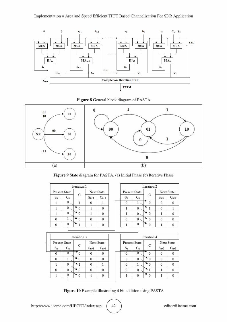
3.3. Parallel Asynchronous Self-Timed Adder (PASTA)
The design of PASTA is regular and uses half-adders (HAs) along with multiplexers requiring
minimal interconnections [11]. Thus, it is suitable for VLSI implementation. The design works
in a parallel manner for independent carry chain blocks. The adder first accepts two input
operands to perform half additions for each bit. Subsequently, it iterates using earlier generated
carry and sums to perform half-additions repeatedly until all carry bits are consumed and settled
at zero level. The general architecture of the adder is shown in Figure 8. The selection input for
two-input multiplexers corresponds to the Req handshake signal and will be a single 0 to 1
transition denoted by SEL. It will initially select the actual operands during SEL = 0 and will
switch to feedback/carry paths for subsequent iterations using SEL = 1. The feedback path from
the HAs enables the multiple iterations to continue until the completion when all carry signals
will assume zero values.
In Figure 9, two state diagrams are drawn for the initial phase and the iterative phase of the
proposed architecture. Each state is represented by (Ci+1 Si) pair where Ci+1, Si represent carry
out and sum values, respectively, from the ith bit adder block. During the initial phase, the
circuit merely works as a combinational HA operating in fundamental mode. It is apparent that
due to the use of HAs instead of FAs, state (11) cannot appear. During the iterative phase (SEL
= 1), the feedback path through multiplexer block is activated. The carry transitions (Ci ) are
allowed as many times as needed to complete the recursion. From the definition of fundamental
mode circuits, the present design cannot be considered as a fundamental mode circuit as the
input–outputs will go through several transitions before producing the final output. It is not a
Muller circuit working outside the fundamental mode either as internally, several transitions
will take place, as shown in the state diagram. This is analogous to cyclic sequential circuits
where gate delays are utilized to separate individual states. 4 bit addition using PASTA is
illustrated using Figure 10 by taking the following values as A=1101 (13); B=1010 (10);
Cin=0001 (1); A+B+Cin=11000 (24). The simulation result of PASTA is as shown in Figure
11.
Implementation o Area and Speed Efficient TPFT Based Channelization For SDR Application
http://www.iaeme.com/IJECET/index.asp 42 [email protected]
Figure 8 General block diagram of PASTA
(a) (b)
Figure 9 State diagram for PASTA. (a) Initial Phase (b) Iterative Phase
Figure 10 Example illustrating 4 bit addition using PASTA

P. Sri Lekha and Dr. K. Pushpa
http://www.iaeme.com/IJECET/index.asp 43 [email protected]
Figure 11 Simulation results of PASTA
4. RESULTS AND DISCUSSION
The TPFT based channelization structure shown in Figure 1 had been designed by making use
of Verilog HDL. The synthesis and simulation results were produced making use of Xilinx ISE
14.5 for the Vertex6 family device.
The output of the in commutator depends on the operation of the switch. The output of the
in commutator are Up and Down. When the switch is 1 then the Up value will be real (Re) part
and the Down value will be imaginary (Im) part and vice-versa when the switch is 0. The output
wave form of the in commutator is shown in Figure 12.
Figure 12 Simulation results of In commutator
The input to the transposed half band filter are obtained by the output of the In commutator.
Half band filters in the PE1 are implemented with a two-phase structure because they are
decimated by two the values which are exported from the In commutator the two branches of a
half band filter are time-multiplexed by the real and imaginary parts of the input data. The
outputs of the transposed half band filters are Band 1, Band 2, Band 3 and Band 4. By reversing
the sign of the Up-output data of band 1, we can get the Up-output data of band 3. In the same
way, we can get the Up-output data of band 4 from the Up-output data of band 2. By replacing
the final adder with subtractor, we can get the filtered data of band 3 from the output results of
two branch filters of band 1. In the same way, the filtered data of band 4 can be obtained from
the output results of two branch filters of band 2.Finally, Band 1, Band 2, Band 3 and Band
4are the outputs of the transposed half band filter. The output wave forms of the transposed half
band filter are shown in Figure 13.
Figure 13 Simulation result of Transposed half band filter
Implementation o Area and Speed Efficient TPFT Based Channelization For SDR Application
http://www.iaeme.com/IJECET/index.asp 44 [email protected]
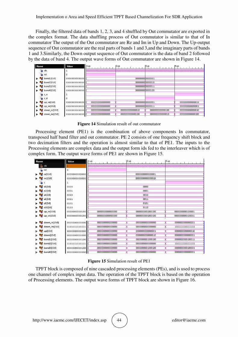
Finally, the filtered data of bands 1, 2, 3, and 4 shuffled by Out commutator are exported in
the complex format. The data shuffling process of Out commutator is similar to that of In
commutator The output of the Out commutator are Re and Im in Up and Down. The Up-output
sequence of Out commutator are the real parts of bands 1 and 3,and the imaginary parts of bands
1 and 3.Similarly, the Down output sequence of Out commutator is the data of band 2 followed
by the data of band 4. The output wave forms of Out commutator are shown in Figure 14.
Figure 14 Simulation result of out commutator
Processing element (PE1) is the combination of above components In commutator,
transposed half band filter and out commutator. PE 2 consists of one frequency shift block and
two decimation filters and the operation is almost similar to that of PE1. The inputs to the
Processing elements are complex data and the output form ids fed to the interleaver which is of
complex form. The output wave forms of PE1 are shown in Figure 15.
Figure 15 Simulation result of PE1
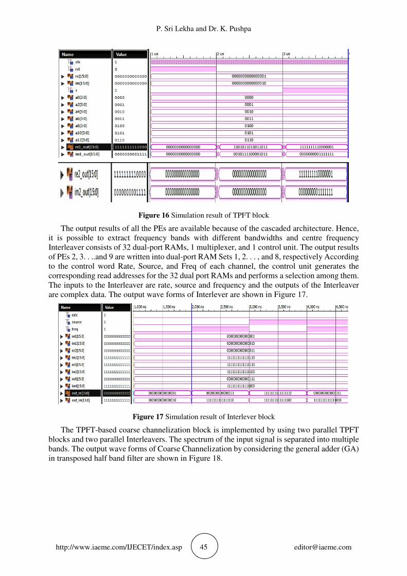
TPFT block is composed of nine cascaded processing elements (PEs), and is used to process
one channel of complex input data. The operation of the TPFT block is based on the operation
of Processing elements. The output wave forms of TPFT block are shown in Figure 16.
P. Sri Lekha and Dr. K. Pushpa
http://www.iaeme.com/IJECET/index.asp 45 [email protected]
Figure 16 Simulation result of TPFT block
The output results of all the PEs are available because of the cascaded architecture. Hence,
it is possible to extract frequency bands with different bandwidths and centre frequency
Interleaver consists of 32 dual-port RAMs, 1 multiplexer, and 1 control unit. The output results
of PEs 2, 3. . ..and 9 are written into dual-port RAM Sets 1, 2. . . , and 8, respectively According
to the control word Rate, Source, and Freq of each channel, the control unit generates the
corresponding read addresses for the 32 dual port RAMs and performs a selection among them.
The inputs to the Interleaver are rate, source and frequency and the outputs of the Interleaver
are complex data. The output wave forms of Interlever are shown in Figure 17.
Figure 17 Simulation result of Interlever block
The TPFT-based coarse channelization block is implemented by using two parallel TPFT
blocks and two parallel Interleavers. The spectrum of the input signal is separated into multiple
bands. The output wave forms of Coarse Channelization by considering the general adder (GA)
in transposed half band filter are shown in Figure 18.

Implementation o Area and Speed Efficient TPFT Based Channelization For SDR Application
http://www.iaeme.com/IJECET/index.asp 46 [email protected]
Figure 18 Simulation result of Coarse Channelization block
Similar analysis is carried out for implementation of TPFT based Coarse Channelization by
considering different adders like RCA, CLA and PASTA and the results are tabulated in Table
1.
Table 5.1 Comparison of results in terms of area utilization and time delay for various Adders
S.No Parameter
Existing
method
(GA)
Proposed
method 1
(RCA)
Proposed
method 2
(CLA)
Proposed
method 3
(PASTA)
1 Number of slice
registers 20471 10318 10319 7090
2 Number of slice LUT’s 16218 12759 13592 12262
3 Time delay (ns) 33.76 9.718 5.822 5.962
5. COMPARISON OF EXISTING METHOD AND PROPOSED
METHODS
In this section, we present the comparison of simulation results for different architectures using
different adders (RCA, CLA and PASTA) which are used for the implementation of TPFT
based channelization. The results obtained for various adders in terms of area utilization and
time delay are tabulated in Table 5.1. The bar chart shown in Figure 19 illustrates the number
of slice register and LUT’s utilized by various adders used in the implementation of TPFT based
channelization. It can be seen that the number of slice registers reduced by 50% for RCA and
CLA based architecture, whereas by 65% are PASTA based architecture when compared with
the existing architecture. Similarly, the number of slice LUT’s reduced by 21% for RCA, 16%
for CLA and 25% for PASTA was observed when compared with the existing method. Overall,
we can see a clear decrease in area utilization for PASTA based architecture which is used in
the implementation of TPFT based channelization. The bar chart shown in Figure 20 compares
the time delay for different architectures based on different adders like RCA, CLA and PASTA
with the existing architecture. From the graph, it is evident that the time delay was decreased
by 71.21%, 82.75% and 82.34% for architectures based on RCA, CLA and PASTA adders
respectively when compared to existing one.

P. Sri Lekha and Dr. K. Pushpa
http://www.iaeme.com/IJECET/index.asp 47 [email protected]
Figure 19 Area utilization of various architectures using different adders
Figure 20 Time delay of various architectures using different adders
6. CONCLUSIONS
In this paper, we have implemented the TPFT based channelization technique by considering
different types of adders like RCA, CLA and PASTA. A comparative study among the existing
and proposed methods was also done using Xilinx tool for vertex family. The number of slice

Implementation o Area and Speed Efficient TPFT Based Channelization For SDR Application
http://www.iaeme.com/IJECET/index.asp 48 [email protected]
registers and LUT’s in the existing system is 20471 and 16218, while that of proposed PASTA
architecture is 7090 and 12262 is observed with minimum area utilization. Similarly, the delay
of the existing method is 33.76 ns while the minimum delay of 5.962 ns was observed for
proposed method 3. This proves the efficiency of PASTA based proposed architecture both in
terms of area and delay. In implementation of TPFT based channelization technique, adders
which are used in transposed half-band filters can be replaced by PASTA adder to achieve low
area and minimum delay. The proposed architecture seems to be remarkably suitable for
channelization where area and delay need to be optimized.
REFERENCES
[1] R. Mahesh, A. P. Vinod, E. M.-K. Lai, and A. Omondi. Filter bank channelizers for multi-
standard software defined radio receivers. J. Signal Process. Syst., 62(2), pp. 2011, pp. 157–
171.
[2] Vinod, A. P., Premkumar, A. B., & Lai, E. M. K. An optimal Entropy coding scheme for
efficient implementation of pulse shaping FIR filters in digital receivers. Proceedings of
IEEE International Symposium on Circuits and Systems, Bangkok, Thailand, 4, 2003, pp.
229–232.
[3] Vinod, A. P., & Lai, E. M-K. Low Power and High- Speed implementation of FIR filters
for software defined radio receivers. IEEE Transactions on Wireless Communications, 5(7),
2006, pp. 1669–1675.
[4] T. Hentschel. Channelization for software defined base-stations. Ann. Telecommun., 57(5–
6), 2002, pp. 386–420.
[5] Kim, C., Shin, Y., Im, S., & Lee, W. SDR-based digital channelizer/de-channelizer for
multiple CDMA signals. Proceedings of IEEE Vehicular technology Conference, 6, 2000,
pp. 2862–2869.
[6] Lillington, J. Comparison of wideband channelization architectures. 2003.
http://www.techonline.com/community/techgroup/ dsp/tech paper/33204.
[7] Lillington, J. TPFT–Tunable pipelined frequency transform. RF Engines Ltd, 2002,
Technical Report. http://www.rfel.com/ whipapdat.asp.
[8] Xue Liu, Ze-Ke Wang, Qing-Xu Deng. Design and FPGA implementation of a
reconfigurable 1024 channel channelization architecture for SDR application. IEEE
Transactions on Very Large Scale Integration (VLSI) Systems, 24(7), 2016, pp. 2449-2461.
[9] K. Revathi and Dr. K. Pushpa. Design and performance analysis of various adders for
accumulation unit of RRC filter. National Conference on Recent Advances in
Communication and Electronics Engineering RACEE-2016, 21st-22nd October 2016.
[10] Sharanagouda N Patil, R.M.Vani and P.V.Hunagund, Data Security Using Advanced
Encryption Standard (AES) In Reconfigurable Hardware For SDR Based Wireless Systems,
Volume 6, Issue 1, January (2015), pp. 95-100, International Journal of Computer
Engineering and Technology.
[11] D. Lalitha Kumari and Prof. M. N. Giri Prasad, A Review Paper on Performance Analysis
of MIMO Based OFDMA System Under Fading Channel, International Journal of
Electronics and Communication Engineering and Technology, 8(1), 2017, pp. 32–42
[12] R.Uma, VidyaVijayan, M.Mohanapriya, and Sharon Paul. Area, Delay and Power
Comparison of Adder Topologies. International Journal of VLSI Design & Communication
Systems, 3(1), 2012, pp.153-168.
[13] Mohammed Ziaur Rahman, Lindsay Kleeman, and Mohammad Ashfak Habib. Recursive
Approach to the Design of a Parallel Self-Timed Adder. IEEE Transactions on Very Large
Scale Integration (VLSI) Systems, 23(1), 2015, pp.213-217.


![M05 arith1.ppt [호환 모드] · 2016-10-31 · Ripple Carry Adder-4-bit ripple carry adder-LSB에서발생된carry가MSB까지전파된후에야sum 계산완료-Carry의전파가adder의계산시간결정](https://img.dokumen.tips/doc/110x75/5e6dfaba8472c611153db48f/m05-eeoe-2016-10-31-ripple-carry-adder-4-bit-ripple-carry-adder-lsboeeoefeoecarryemsbeoeoeoeeoesum.jpg)