Embed Size (px)
Citation preview

Monza® X-2K Dura Datasheet Copyright © 2013, Impinj, Inc. i
Impinj® Monza® X-2K Dura Datasheet Rev 1.51 March 24th , 2014
Part Order #: IPJ-P6001-Q2AT
Monza® X-2K Dura is a UHF Gen2 RFID
IC product with 2176 bits of Non Volatile
Memory (NVM) and an I2C interface.
As an I2C device Monza® X-2K Dura
operates as a standard I2C EEPROM. The
contents of this EEPROM can also be
accessed wirelessly via the UHF Gen2 RFID
Protocol.
Features
EPCglobal and ISO 18000-63 compliant,
Gen2V2 compliant.
2176 bits of user NVM
4 One Time Programmable (OTP)
blocks (1664/2160 bits) via
blockpermalock feature supported by
both I2C and EPC Gen2 interface
QT for read control and data privacy on
RF link
I2C slave interface with NVM read and
write
–17dBm typical read sensitivity when
using a single RF antenna port, -24dBm
with DC input
–19.5dBm typical read sensitivity when
using dual RF antenna ports
–12dBm typical write sensitivity when
using a single RF antenna port
I2C control of RF access
Write wakeup mode
Name Description Characteristic
RF1_P Differential RF Input
Port 1
1.6kΩ, 1pF
–17 dBm single-
port sensitivity;
–19.5 dBm True3D
sensitivity
RF1_N
RF2_P Differential RF Input
Port 2 RF2_N
DCI DC Input 1.6–3.6V
SCL I2C Clock Input VIH/L=70% / 30%
DCI
IOL=6mA @ 0.4V SDA I2C Data Input
GND


Monza® X-2K Dura Datasheet
Monza® X-2K Dura Datasheet Copyright © 2013, Impinj, Inc. 1
Table of Contents
1 Introduction ........................................................................................................................2 1.1 Scope ..................................................................................................................................2 1.2 Reference Documents .........................................................................................................2
2 Functional Description .......................................................................................................3 2.1 Reader Communications (Gen2/RF Commands) ...............................................................3 2.2 Support for Optional Gen 2 Commands .............................................................................4 2.3 I2C Interface (SDA, SCL, DCI Pins) .................................................................................5 2.4 I2C Memory Map ...............................................................................................................7
2.5 I2C Control of Monza® X-2K Dura Behavior ...................................................................9 2.6 Monza® X-2K Dura I2C and Gen2 Lock Bits ...................................................................9
2.7 Monza® X-2K Dura I2C and Gen2 BlockPermalock ......................................................10 2.8 Monza® X-2K Dura I2C Control of Config[1:0] Bits .....................................................11 2.9 Monza® X-2K Dura Control of the QT Function ............................................................11 2.10 Monza® X-2K Dura I2C Control of Gen2 Response to Ack Command .........................11
2.11 RF Access Control ............................................................................................................12 2.12 Gen2/I2C Arbitration ........................................................................................................12
2.13 Write Wakeup Mode ........................................................................................................14 3 Chip Characteristics ..........................................................................................................15
3.1 Physical Characteristics ....................................................................................................15
3.2 Absolute Maximum Ratings .............................................................................................16 3.3 Reflow Temperature Profile .............................................................................................17
3.4 Electrical Characteristics ..................................................................................................17
3.5 Memory Characteristics ....................................................................................................20
3.6 RF Functionality ...............................................................................................................21 3.7 I2C Characteristics ...........................................................................................................21
3.8 NVM Usage Model ..........................................................................................................22 3.9 Environmental Compliance ..............................................................................................22
4 Product Delivery Specifications .......................................................................................23
4.1 Marking Specification ......................................................................................................23 4.2 Tape and Reel Specification .............................................................................................24
5 Errata ................................................................................................................................25 6 Introducing Impinj® Monza® X-8K Dura ....................... Error! Bookmark not defined.
7 Ordering Information ........................................................................................................27 Notices 28

Monza® X-2K Dura Datasheet
Monza® X-2K Dura Datasheet Copyright © 2013, Impinj, Inc. 2
1 Introduction
1.1 Scope This datasheet defines the physical and logical specifications for Gen 2-compliant Monza X-2K
Dura tag chip, a reader-talks-first, radio frequency identification (RFID) component operating in
the UHF frequency range.
1.2 Reference Documents EPC
TM Radio Frequency Identity Protocols Class-1 Generation-2 UHF RFID Protocol for
Communications at 860 MHz – 960 MHz, Version 1.2.0 (Gen 2 Specification). The conventions
used in the Gen 2 Specification (normative references, terms and definitions, symbols,
abbreviated terms, and notation) were adopted in the drafting of this Monza X-2K Dura Tag
Chip Datasheet. Users of this datasheet should familiarize themselves with the Gen 2
Specification.
EPC™ Tag Data Standards Specification
EPCglobal “Interoperability Test System for EPC Compliant Class-1 Generation-2 UHF RFID
Devices” v.1.2.4, August 4, 2006. (Monza X-2K Dura tag chips are compliant with this Gen 2
interoperability standard.)
I2C Specification Rev. 03, June 19 2007, NXP Doc UM10204

Part Order#: IPJ-P6001-Q2AT
Monza® X-2K Dura Datasheet Copyright © 2013, Impinj, Inc. 3
2 Functional Description Monza® X-2K Dura chips enable users to communicate wirelessly with the processor inside
electronic devices using standard Gen 2 RFID readers, unlocking many new benefits for
consumer electronics manufacturers, retailers and end users. Monza X-2K Dura connects to the
processor of an electronic device through a standard I2C bus. This enables the processor to read
and write the Monza X chip memory with information that is accessible to UHF Gen 2 RFID
readers even when the electronic device is powered off. By enabling electronic devices to
communicate with RFID readers, Monza X chips deliver a wide range of extended capabilities
such as theft deterrence in the supply chain and device configuration/upgrades at point of sale
and beyond.
Figure 1 – Monza X-2K Dura connects with microprocessor through I2C bus
2.1 Reader Communications (Gen2/RF Commands) A reader communicates with Monza® X-2K Dura using standard Gen2 RFID commands. Please
see the EPCglobal Class-1 Generation-2 UHF RFID Air-Interface Protocol V1.2.0 for details.
The Gen 2 memory map is shown in Figure 2. Fields in blue text are read only. Reserved
memory bank words 4-10 are read only.

Monza® X-2K Dura Datasheet Copyright © 2013, Impinj, Inc. 4
Figure 2– Gen2 Interface Memory Map
2.2 Support for Optional Gen 2 Commands Following optional Gen 2 commands are supported:
Command Code Length Details
Access 11000110 56
BlockWrite 11000111 >57 • Accepts valid one-word commands
• Accepts valid two-word commands if
pointer is an
even value
• Returns error code (000000002) if it
receives a valid
two-word command with an odd value
pointer
• Returns error code (000000002) if it
receives a
command for more than two words
• Does not respond to block write
commands of zero
words
Part Order#: IPJ-P6001-Q2AT
Monza® X-2K Dura Datasheet Copyright © 2013, Impinj, Inc. 5
Command Code Length Details
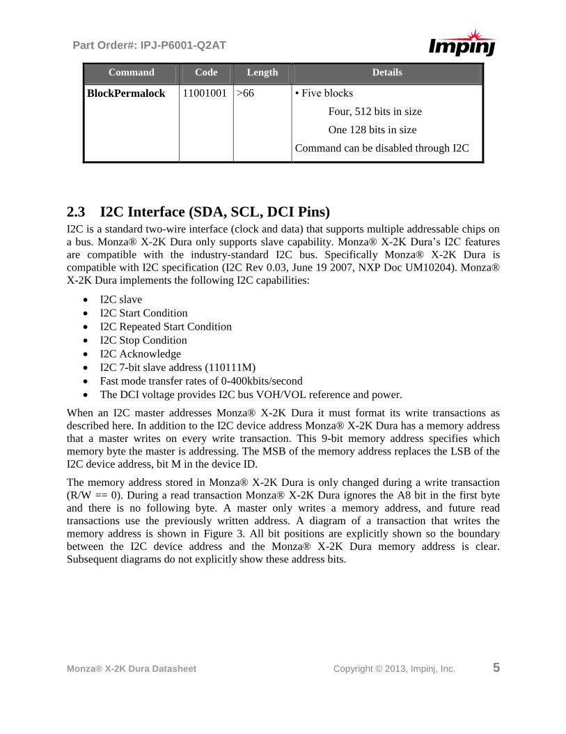
BlockPermalock 11001001 >66 • Five blocks
Four, 512 bits in size
One 128 bits in size
Command can be disabled through I2C
2.3 I2C Interface (SDA, SCL, DCI Pins) I2C is a standard two-wire interface (clock and data) that supports multiple addressable chips on
a bus. Monza® X-2K Dura only supports slave capability. Monza® X-2K Dura’s I2C features
are compatible with the industry-standard I2C bus. Specifically Monza® X-2K Dura is
compatible with I2C specification (I2C Rev 0.03, June 19 2007, NXP Doc UM10204). Monza®
X-2K Dura implements the following I2C capabilities:
I2C slave
I2C Start Condition
I2C Repeated Start Condition
I2C Stop Condition
I2C Acknowledge
I2C 7-bit slave address (110111M)
Fast mode transfer rates of 0-400kbits/second
The DCI voltage provides I2C bus VOH/VOL reference and power.
When an I2C master addresses Monza® X-2K Dura it must format its write transactions as
described here. In addition to the I2C device address Monza® X-2K Dura has a memory address
that a master writes on every write transaction. This 9-bit memory address specifies which
memory byte the master is addressing. The MSB of the memory address replaces the LSB of the
I2C device address, bit M in the device ID.
The memory address stored in Monza® X-2K Dura is only changed during a write transaction
(R/W == 0). During a read transaction Monza® X-2K Dura ignores the A8 bit in the first byte
and there is no following byte. A master only writes a memory address, and future read
transactions use the previously written address. A diagram of a transaction that writes the
memory address is shown in Figure 3. All bit positions are explicitly shown so the boundary
between the I2C device address and the Monza® X-2K Dura memory address is clear.
Subsequent diagrams do not explicitly show these address bits.

Monza® X-2K Dura Datasheet Copyright © 2013, Impinj, Inc. 6
S D5 D4 D3 D2 D1 D0 A8 0 A A7 A6 A5 A4 A3 A2 A1 A0 A P
Start Stop
Acknowledge
from slave
Acknowledge
from slaveI2C Device Address
Memory Address
(Byte Aligned)
R/W
Figure 3 – Addressing the device and setting the memory address
When performing an NVM write a master transmits data after the memory address. Monza® X-
2K Dura’s NVM is organized as 16-bit words. Writes must align on word boundaries. The NVM
allows one- or two-word writes (equivalent to two- or four-byte writes). When executing a one-
word write Monza® X-2K Dura ignores the LSB (A0) of the memory address. When executing a
two-word write Monza® X-2K Dura ignores the two LSBs (A1, A0) of the memory address. If
the write transaction is valid then Monza® X-2K Dura begins the NVM write after receiving a
stop from the I2C master. Monza® X-2K Dura will not respond to subsequent I2C transactions
for the duration of the NVM write operation. The write time for one- and two-word write
operations is the same. A one-word NVM write transaction is shown in Figure 4.
Monza® X-2K Dura may observe several types of invalid NVM-write transactions. If a master
sends one or three data bytes then Monza® X-2K Dura will not perform the write (recall that
Monza® X-2K Dura writes 16-bit words). If a master sends more than two words then Monza®
X-2K Dura will not perform the write. Monza® X-2K Dura also checks the memory address and
will not perform a write if the address is invalid (but note that Monza® X-2K Dura updates its
memory address even if the address is invalid).
Start R/W
Acknowledge
from slaveAcknowledge
from slave
Acknowledge
from slaveAcknowledge
from slave
Stop
S 0 A A A A PD A T AI2C ADDR MEM ADDR D A T A
Figure 4 – One-word Monza® X-2K Dura write transaction
Figure 5 shows a read transaction. The read starts from the stored address. Monza® X-2K Dura
increments the address as it sends each data byte. Monza® X-2K Dura ignores the MSB of the
memory address when the R/W==1.
Start
Acknowledge
from slaveNack
from master
Acknowledge
from masterAcknowledge
from master
StopR/W Auto increment byte address after each byte sent
S 1 A A A A PD A T AD A T AI2C ADDR D A T A
Figure 5 – Monza® X-2K Dura read transaction
Reads start from the stored address and continue to the end of memory, at which point Monza®
X-2K Dura will cease exchanging data over I2C. Monza® X-2K Dura will send all ones if the
master continues to read beyond the end of the memory. To read from a new location the master

Part Order#: IPJ-P6001-Q2AT
Monza® X-2K Dura Datasheet Copyright © 2013, Impinj, Inc. 7
must send a new address. The master may halt the read at a byte boundary and later initiate a
new read transaction starting from that byte. For completeness the combined write transaction
then read transaction is shown in Figure 6.
R/W
Acknowledge
from slaveAcknowledge
from master
StopR/W
Acknowledge
from slaveAcknowledge
from slave
Nack
from master
Start Repeated Start
Auto increment byte address after each byte sent
S 0 A A S 1 A A A PD A T AMEM ADDR I2C ADDR D A T AI2C ADDR
Figure 6 – Write transaction to set address followed by repeated start and read transaction.
Monza® X-2K Dura ignores all Gen2 Lock, Kill permissions when reading / writing over I2C.
The I2C port has read access to the entire NVM. The I2C port has write access to most, but not
all, of the NVM. Monza® X-2K Dura precludes a master from writing its manufacturing
calibration fields (shown as Reserved in the I2C memory map of Figure 7); these locations are
read-only.
2.4 I2C Memory Map Gen 2 and I2C have different views on how a memory map is organized. In I2C everything is
done according to bytes. One uses byte addressing, byte writing, and byte reading. In Gen2
things are done in terms of bits or 16 bit words.
Monza® X-2K Dura is a hybrid of these two approaches. It forces I2C to do one word or two
word writes, but allows for byte wise reading and addressing. When reading via I2C the first bit
read is always bit seven within the byte. The next byte read is at the next higher I2C byte
address. The I2C memory map in byte wise format is shown in Figure 7.
An additional memory map that shows bit addressing from I2C in a word wise format is shown
in Figure 8.

Monza® X-2K Dura Datasheet Copyright © 2013, Impinj, Inc. 8
Figure 7 – I2C Interface Memory Map in a Byte Wise format

Part Order#: IPJ-P6001-Q2AT
Monza® X-2K Dura Datasheet Copyright © 2013, Impinj, Inc. 9
Figure 8 – I2C Interface Memory Map in a Word Wise format
2.5 I2C Control of Monza® X-2K Dura Behavior The I2C interface can control Monza® X-2K Dura behavior by writing to bytes 8 or 9, 20 or 21,
and 22 or 23. The following sections describe how control bits in these words change the
behavior.
2.6 Monza® X-2K Dura I2C and Gen2 Lock Bits The lock bits for the kill password (LOCK_KILL[1:0]), the access password
LOCK_ACCESS[1:0]), the EPC memory bank (LOCK_EPC[1:0]), and the USER memory
bank (LOCK_ USER[1:0]) are in byte eight of memory. In each of these lock bit pairs bit one
corresponds to pwd-write or pwd-read/write and bit zero corresponds to the permalock bit. Note
that the I2C can always change the state of these bits and that their permissions only apply to the
RF Gen2 interface.
Table 2.1 – Lock Bit-field functionality
pwd-write permalock Description
0 0 Associated memory bank is writeable from either the open or secured
states.
0 1 Associated memory bank is permanently writeable from either the open or
secured states and may never be locked.
1 0 Associated memory bank is writeable from the secured state but not from
the open state.

Monza® X-2K Dura Datasheet Copyright © 2013, Impinj, Inc. 10
1 1 Associated memory bank is not writeable from any state.
pwd-
read/write permalock Description
0 0 Associated password location is readable and writeable from either the
open or secured states.
0 1 Associated password location is permanently readable and writeable from
either the open or secured states and may never be locked.
1 0 Associated password location is readable and writeable from the secured
state but not from the open state.
1 1 Associated password location is not readable or writeable from any state.
2.7 Monza® X-2K Dura I2C and Gen2 BlockPermalock Monza® X-2K Dura will segments user memory into five blocks. Blocks zero through four may
be blockpermalocked from either the Gen2 interface or the I2C interface. A blockpermalocked
block allows reads but not writes to the block. Blockpermalocking is permanent for blocks one
through four and may not be unlocked from either interface. The blockpermalock may be
undone for block zero from the I2C interface and I2C ignores the blockpermalock permission for
block zero.
The five blocks as seen from the I2C interface are shown in Figure 9. The five blocks in the
User memory bank as seen from the Gen2 interface are:
Block 0: bit address 0 to bit address (512 bit block size)
Block 1: bit address 512 to bit address 1023 (512 bit block size)
Block 2: bit address 1024 to bit address 1535 (512 bit block size)
Block 3: bit address 1536 to bit address 2047 (512 bit block size)
Block 4: bit address 2048 to bit address 2175 (128 bit block size)
Please see the Gen2 specification for details on how a reader may lock the memory via
BlockPermaLock command.
The mechanism for a microprocessor permalocking over I2C is as follows: Execute a one-word
(2 byte) write to bytes eight and nine (word address four). There are five blockpermalock bits in
byte nine that control the write permission to the five user-memory blocks. Monza® X-2K Dura
will bitwise OR each of the current permalock bits with the four bits corresponding to blocks one
through four and write the updated word into NVM. Block zero may be unlocked via the I2C
interface. Monza® X-2K Dura does not allow unlocking of blockpermalocked memory in blocks
one through four via either the Gen2 interface or I2C interface.
To control the Gen2 interface access to the BlockPermalock command the I2C interface will
have a BlockPermalock command enable bit that only it can write to. When the bit is set
Monza® X-2K Dura will execute valid BlockPermalock commands and when it is cleared it will
ignore all BlockPermalock commands. The location of the BPL_EN bit is in bit five of byte 21.

Part Order#: IPJ-P6001-Q2AT
Monza® X-2K Dura Datasheet Copyright © 2013, Impinj, Inc. 11
Figure 9 – BlockPermaLock blocks as seen from the I2C interface
2.8 Monza® X-2K Dura I2C Control of Config[1:0] Bits The CONFIG[1:0] bits contain important configuration that must be preserved. Users must take
care not to accidentally reprogram them when writing to bytes 8 and 9. The I2C master must read
bytes 8 and 9. Then apply the values for CONFIG[1:0] to the new data that is written. The
following logic operation for the word to be sent over the I2C bus will achieve this.
SENT_WORD = (OLD_WORD & 0x0003) | (NEW_WORD & 0xFFFC)
2.9 Monza® X-2K Dura Control of the QT Function The QT_SR and QT_MEM bits control in byte 21 control the QT functionality of Monza® X-2K
Dura. They have no effect on I2C operation and only change RF Gen2 behavior. The two bits
operate independently from each other. The QT_SR bit turns on Monza® X-2K Dura’s short
range mode when it is set. When Monza® X-2K Dura is in short range, operations in OPEN or
SECURED states are required to be close to the reader. Note, however, that if the Monza® X-
2K Dura antenna has a gain < -9dBi, there will be no OPEN or SECURED access through the
RF port when the QT_SR bit is set. The QT_MEM bit controls how Monza® X-2K Dura’s
memory appears to the Gen2 interface. When the bit is set Monza® X-2K Dura is in public
mode: user memory bank is hidden, TID serialization is hidden, and uses its QT_EPC in the EPC
bank. When the bit is cleared Monza® X-2K Dura is in private mode and all of its memory is
exposed. The memory map in Figure 2 shows the Monza® X-2K Dura memory in private mode.
The DCI_EN_RF_EN bit and the RF_DIS[1:0] bits in byte 21 are covered in the section on RF
access control.
2.10 Monza® X-2K Dura I2C Control of Gen2 Response to Ack
Command The length field in byte 22 may be written from I2C. The length field specifies the number of
words backscattered in response to a Gen2 Ack command. Byte 22 also contains an NVM space
Monza® X-2K Dura Datasheet Copyright © 2013, Impinj, Inc. 12
for the UMI bit which may be read or written from I2C. The NVM bit is not used since it is
automatically calculated per the Gen2 specification. The Gen2 UMI bit is calculated from the
bitwise or of bits five through zero in byte 40.
2.11 RF Access Control Monza® X-2K Dura provides three levels of control over RF access as follows:
1. Setting either or both the RF1_DIS or RF2_DIS bits in byte 21 of the NVM disables RF
access on the corresponding RF port. These bits are accessible only to I2C, not RF. The
factory defaults are 0, enabling RF1 and RF2.
2. Setting the DCI_RF_EN bit to 0 in byte 21 of the NVM inhibits all RF access when DCI
voltage is present. This takes precedence over the state of the RF1_DIS, RF2_DIS bit in
#1 above. This bit is also only accessible from I2C, not RF. This bit is set by factory
default to 0. Thus, by default, there is RF access to RF1, RF2 when DCI voltage is NOT
present and no RF access when DCI voltage is present. The specification VRFON
determines the DCI voltage that inhibits RF.
3. Setting the KILL bit 2 in byte 9 of the NVM will inhibit all RF access. This bit can be set
from RF using a Gen2 KILL command or by writing from I2C. This is the normal
mechanism for a reader to disable a chip. This KILL bit takes precedence over both #1
and #2 above. I2C can re-write this bit back to 0 and thus reverse and RF KILL
command. The factory default for KILL is 0.
The factories defaults are set so Monza® X-2K Dura operates like any other RFID tag when DCI
voltage is not present. When DCI voltage is present the default behavior, through mechanism #2
above, is to inhibit all RF access. The KILL bit is always set to 0 at the factory by Gen2
definition. In conventional RFID chips once this bit is set to 1 a chip is dead and can never be
resurrected. Monza® X-2K Dura, having a hard wired I2C interface, allows un-doing the KILL
operation from I2C.
2.12 Gen2/I2C Arbitration If the DCI_RF_EN bit is set to one then Monza® X-2K Dura has three different operating states
as shown in Figure 10. The states are “Internal Control”, “I2C Control”, and “Idle or RF
Receive”. If the DCI_RF_EN bit is set to zero then Monza® X-2K Dura will not respond to RF
commands when in the Idle or RF Receive state.
Internal Control: Monza® X-2K Dura is in Internal Control when (1) executing an initialization
sequence, (2) writing the NVM or (3) backscattering a response to an RF command. When in
Internal Control Monza® X-2K Dura ignores I2C transactions or RF commands.
I2C Control: Monza® X-2K Dura is in I2C Control when a master is issuing commands to
Monza® X-2K Dura over the I2C bus. I2C Control starts when Monza® X-2K Dura detects a
matching device ID and is not under Internal Control. The I2C bus master releases control of
Monza® X-2K Dura either by ending a transaction with a stop bit or by issuing a subsequent
start with a non-matching device ID. If Monza® X-2K Dura was commanded to perform an
NVM write then it moves to Internal Control, otherwise it returns to idle. When in I2C Control
Monza® X-2K Dura ignores all RF commands. Note that the master may stall the I2C bus (by
holding SCL low) in the middle of a transaction and prevent RF access until releasing the bus.
Idle or RF Receive: Monza® X-2K Dura is in Idle or RF Receive when receiving an RF
command or when idle. After receiving a command Monza® X-2K Dura transitions to Internal

Part Order#: IPJ-P6001-Q2AT
Monza® X-2K Dura Datasheet Copyright © 2013, Impinj, Inc. 13
Control to execute the command. Executing a command may cause Monza® X-2K Dura to (1)
backscatter a reply (2) write to NVM or (3) change internal states. An I2C transaction may
interrupt Monza® X-2K Dura in Idle or RF Receive– by this means the I2C port exercises
priority over the RF port and may not be locked out. Note that I2C is locked out when Monza®
X-2K Dura transitions to Internal Control to execute the command.
In certain operating states and under certain conditions Monza® X-2K Dura may appear
unresponsive to an I2C master for up to 20 milliseconds (During a slow Gen2 backscatter). This
datasheet recommends that an I2C master have a retry algorithm that can accommodate Monza®
X-2K Dura being busy.
Figure 10 – Monza® X-2K Dura operating states

Monza® X-2K Dura Datasheet Copyright © 2013, Impinj, Inc. 14
2.13 Write Wakeup Mode Monza® X-2K Dura has a wake up feature that is tied to writes being performed over the Gen2
interface. In order to enable this feature the I2C master must set the WWU bit (bit 6 of byte 21)
to one. Then the master must set the Monza® X-2K Dura’s DCI pin to 0V (Sleep mode). The
SCL and SDA lines must remain high, but draw no current. A reader may continue to interact
with Monza® X-2K Dura on the RF ports. If a reader performs a write operation, and the wake
up mode is set, Monza® X-2K Dura will assert the SCL IO pulling the SCL line low for the
duration of the write operation, approximately 4ms. This transition may then be detected by the
sleeping master and used to wake up the system.
Figure 11 – Monza® X-2K Dura write wake up mode schematic and timing diagram

Part Order#: IPJ-P6001-Q2AT
Monza® X-2K Dura Datasheet Copyright © 2013, Impinj, Inc. 15
3 Chip Characteristics
3.1 Physical Characteristics
Parameter Description Condition Min Nom Max Units Comments
IC package Chip package All XQFN 8L 1.65×1.65×0.35mm
Pin count Package pins All 8 pins
2 – Port1 RF+/–
2 – Port2 RF+/–
2 – DCI/gnd
2 – I2C(SDA/SCL)
Figure 12– Packing Dimensions
Monza® X-2K Dura Datasheet Copyright © 2013, Impinj, Inc. 16
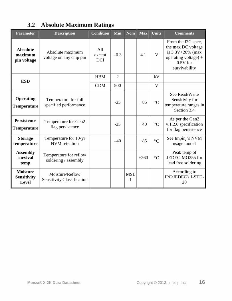
3.2 Absolute Maximum Ratings
Parameter Description Condition Min Nom Max Units Comments
Absolute
maximum
pin voltage
Absolute maximum
voltage on any chip pin
All
except
DCI
–0.3 4.1 V
From the I2C spec,
the max DC voltage
is 3.3V+20% (max
operating voltage) +
0.5V for
survivability
ESD HBM 2 kV
CDM 500 V
Operating
Temperature
Temperature for full
specified performance -25 +85 C
See Read/Write
Sensitivity for
temperature ranges in
Section 3.4
Persistence
Temperature
Temperature for Gen2
flag persistence -25 +40 C
As per the Gen2
v.1.2.0 specification
for flag persistence
Storage
temperature
Temperature for 10-yr
NVM retention –40 +85 C
See Impinj’s NVM
usage model
Assembly
survival
temp
Temperature for reflow
soldering / assembly +260 C
Peak temp of
JEDEC-MO255 for
lead free soldering
Moisture
Sensitivity
Level
Moisture/Reflow
Sensitivity Classification
MSL
1
According to
IPC/JEDEC's J-STD-
20

Part Order#: IPJ-P6001-Q2AT
Monza® X-2K Dura Datasheet Copyright © 2013, Impinj, Inc. 17
3.3 Reflow Temperature Profile
3.4 Electrical Characteristics
Parameter Description Condition Min Nom Max Units Comments
RF Performance
SREAD
Matched RF Input
Read Sensitivity
DRM, M=4
No DC Input -17
dBm
Using DC
Input, Monza
X-2K Dura can
be used in
Battery
Assisted
Passive mode
to increase
read/write
range
With DC
Input at 0C
to +85C
-24 dBm
With DC
Input at 0C
to -25C
-20 dBm
SWRITE
Matched RF Input
Write Sensitivity
DRM, M=4
No DC Input –12
dBm
With DC
Input at 0C
to +85C
-24 dBm
With DC
Input at 0C
to -25C
-20 dBm
Rp Parallel Equivalent
Real Input Impedance
At
Sensitivity 1600 Ohms

Monza® X-2K Dura Datasheet Copyright © 2013, Impinj, Inc. 18
Parameter Description Condition Min Nom Max Units Comments
Cp Parallel Equivalent RF
Input Capacitance 1 pF

Part Order#: IPJ-P6001-Q2AT
Monza® X-2K Dura Datasheet Copyright © 2013, Impinj, Inc. 19
Parameter Description Condition Min Nom Max Units Comments
POWER
VDCI DCI Input Voltage/I2C
Reference 1.6 3.6 V
These DCI
voltages are with
a ±100mV
tolerance
IDCW Current drawn by chip
during write
1.6<VDCI<2.0 100 200 µA
Nominal 80uA at
1.6V 2.0<VDCI<3.6 140 220
IDCI Current drawn by chip
during read or idle
1.6<VDCI<2.0 15 30 µA
2.0<VDCI<3.6 20 40
TPU
Power Up Time.
Time from VDCI
applied until I2C
accepts transactions.
VDCI=1.6V 2 ms
NOTE: I2C will
not interrupt a
write operation.
This could delay
I2C access up to
20ms if RF is
writing.
VRF_EN Max Vdd for which RF
will always be enabled 0.25 V Applies if the
DCI_RF_EN bit
is set to 0.
VRF_DIS Min Vdd for which RF
will always be disabled
Parameter Description Condition Min Nom Max Units Comments
I2C
VIH HIGH-level input
voltage All
70%
%VDCI
From the
section 6 of the
I2Cspecification
VIL
LOW-level input
voltage All
30%
%VDCI
VHYS Input hysteresis All 0.1
V

Monza® X-2K Dura Datasheet Copyright © 2013, Impinj, Inc. 20
Parameter Description Condition Min Nom Max Units Comments
IOL LOW-level output
current VOL=0.4 3
** mA
TOF Output Fall Time Bus C=
40-400pf 20 250 ns
CI Pin Capacitance 10 pF
Total capacitive
load on the
SDA/SCL pins
IIL SCL/SDA Input
Leakage Current
Vin=3.7V
0V<VDCI<3.7V 1 100 nA
Exceeds I2C
spec of 10uA
**IOL is tested with worst case minimum pull-up resistance value of 536 ohms at 2v.
Applications should use as high pull-up resistance as possible consistent with the bus capacitance
for the application. See the I2C specification for choosing pull-up resistor values. Values of 5K
or more are typical in low power applications
3.5 Memory Characteristics
Parameter Description Condition Min Nom Max Units Comments
EPC
memory EPC NVM
In private
mode only 128 bits
User writeable. This memory
is hidden over RF when QT
is enabled.
User
memory Total user NVM
In private
mode only 2176 bits
User defined memory space.
This memory is hidden over
RF when QT is enabled
QT
alternative
EPC
Alternative EPC
presented during RF
singulation
In public
mode only 96 bits
A user can switch the tag’s
RF QUERY–ACK response
from EPC to alternative EPC
using the QT command
Kill/Access
Passwords Password NVM
Access
required 64 bits
Standard 32-bit Gen2 access
and kill passwords
TID
mfg#/serial# TID ROM
In private
mode only 96 bits
TID serial number is hidden
over RF when QT is enabled
Total
Memory Total memory size 2560 bits
TWRITE Memory write time
16 or 32 bits 4.7 5 ms

Part Order#: IPJ-P6001-Q2AT
Monza® X-2K Dura Datasheet Copyright © 2013, Impinj, Inc. 21
3.6 RF Functionality
Parameter Description Condition Min Nom Max Units Comments
Air protocol Gen2 V1.2.0 All No recommissioning;
no blockerase
RF ports Number of RF
ports All 2
Dual-differential RF
ports
RF Port
Disable
NVM Settable bit
per port
The operation of one
or both RF ports may
be disabled by setting
NVM bits through the
I2Cport
DC Blocks RF NVM Settable bit
Option to allow the
presence of DC to
disable both RF ports
3.7 I2C Characteristics
Parameter Description Condition Min Nom Max Units Comments
I2C port Number of ports All 1 Slave I2C
(SCL/SDA)
I2C
functionality
Compatible with
I2C-bus specification
and user manual Rev.
03 – 19 June 2007
All R/W An external device
can R/W memory
Supported
I2C features
Features: Slave Configuration
Start condition mandatory
Stop condition mandatory
Acknowledge mandatory
7-bit slave address mandatory
I2Cwrite size Word size for I2C
write All 16 32 bits
Writes are on word
addresses and not
byte addresses
I2C read size Word size for I2C
read All N×8 bits
May read data 8bits
at a time, where N is
limited by start
address and bank size
I2C memory
arbitration RF/I2C port priority All 1
st
RF/I2C arbitrate for
NVM access
I2C Address I2C Device Address All 110111M
1

Monza® X-2K Dura Datasheet Copyright © 2013, Impinj, Inc. 22
Parameter Description Condition Min Nom Max Units Comments
Transfer
rates
I2C transfer data
rates All 0 400 kbps I2C fast mode
1Monza(R) X-2K Dura operates like most I2C EEPROM devices in that the LSB of the 7-bit I2C
device address is the MSB of the NVM address. The 8 LSBs of the NVM address are sent in the next
I2C byte.
3.8 NVM Usage Model
Condition Retention (years)
Writes per row Total writes Power-on time
10 100 5 yr 50
1k 10k 1 yr 10
10k 100k 2k hours 1
3.9 Environmental Compliance
Requirement Comments
RoHS Monza X-2K Dura is RoHS compliant. It meets the directive
2002/95/EC (RoHS). RoHS declaration letter is available upon
request.
REACH Monza X-2K Dura does not, to our current knowledge, contain
substances above the legal threshold that are on the Candidate
List of Substances of Very High Concern (SVHC). Our
company’s intention is that all products sold to our EU and EEA
customers by our legal entities in Europe are compliant with
REACH regulatory requirements. REACH declaration letter is
available upon request.

Part Order#: IPJ-P6001-Q2AT
Monza® X-2K Dura Datasheet Copyright © 2013, Impinj, Inc. 23
4 Product Delivery Specifications
4.1 Marking Specification
Y= Year of production (1 = 2011, 2 = 2012 …)
WW = Work Week of production
X2 = Product Code (Monza X-2K Dura)
Pin # 1 dot
W2
W
3
Y
1
X4
25

Monza® X-2K Dura Datasheet Copyright © 2013, Impinj, Inc. 24
4.2 Tape and Reel Specification
Parts per reel / Minimum order quantity: 3000

Part Order#: IPJ-P6001-Q2AT
Monza® X-2K Dura Datasheet Copyright © 2013, Impinj, Inc. 25
5 Errata The following table lists the known issues in Monza® X-2K Dura
Issue
Number Description
1
When writing from the I2C block the cache for the PC length field
is not properly updated after I2C writes. The part must be power
cycled to have the cache updated.
2
If QT features are changed from I2C, then the changes don’t take
effect until power is cycled. Specifically, Monza® X-2K Dura
does not recache the RFS_MEM (1=Monza® X-2K Dura is using
the alternate EPC) or RFS_SR (1= tag is in short range) when
written from I2C. It needs to be power cycled for the change to
take effect.

Monza® X-2K Dura Datasheet Copyright © 2013, Impinj, Inc. 26
6 Footprint Compatibility with Impinj® Monza® X-
2K Dura Monza® X-8K Dura (Part Order#: IPJ-P6005-X2AT) is a higher memory capacity version of
Monza® X-2K Dura.
Monza® X-8K Dura is designed to have 8192 bits of user NVM, enabling more OTP blocks. Its
package dimensions are 2.0x2.0x0.35 mm. It is designed to be a drop-in replacement for Monza
X-2K Dura if the layout footprint recommended below is used. For more details about the
Monza® X-8K Dura including product availability, please contact Impinj.
Figure 13 – Recommended common layout footprint for Monza® X-2K Dura and Monza® X-
8K Dura
Part Order#: IPJ-P6001-Q2AT
Monza® X-2K Dura Datasheet Copyright © 2013, Impinj, Inc. 27
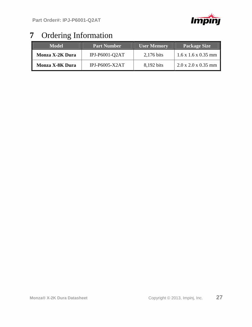
7 Ordering Information
Model Part Number User Memory Package Size
Monza X-2K Dura IPJ-P6001-Q2AT 2,176 bits 1.6 x 1.6 x 0.35 mm
Monza X-8K Dura IPJ-P6005-X2AT 8,192 bits 2.0 x 2.0 x 0.35 mm

Monza® X-2K Dura Datasheet Copyright © 2013, Impinj, Inc. 28
Notices Copyright © 2013, Impinj, Inc. All rights reserved.
Impinj gives no representation or warranty, express or implied, for accuracy or reliability of
information in this document. Impinj reserves the right to change its products and services and
this information at any time without notice.
EXCEPT AS PROVIDED IN IMPINJ’S TERMS AND CONDITIONS OF SALE (OR AS
OTHERWISE AGREED IN A VALID WRITTEN INDIVIDUAL AGREEMENT WITH
IMPINJ), IMPINJ ASSUMES NO LIABILITY WHATSOEVER AND IMPINJ DISCLAIMS
ANY EXPRESS OR IMPLIED WARRANTY, RELATED TO SALE AND/OR USE OF
IMPINJ PRODUCTS INCLUDING LIABILITY OR WARRANTIES RELATING TO
FITNESS FOR A PARTICULAR PURPOSE, MERCHANTABILITY, OR INFRINGEMENT.
NO LICENSE, EXPRESS OR IMPLIED, BY ESTOPPEL OR OTHERWISE, TO ANY
PATENT, COPYRIGHT, MASK WORK RIGHT, OR OTHER INTELLECTUAL PROPERTY
RIGHT IS GRANTED BY THIS DOCUMENT.
Impinj assumes no liability for applications assistance or customer product design. Customers
should provide adequate design and operating safeguards to minimize risks.
Impinj products are not designed, warranted or authorized for use in any product or application
where a malfunction may reasonably be expected to cause personal injury or death or property or
environmental damage (“hazardous uses”) or for use in automotive environments. Customers
must indemnify Impinj against any damages arising out of the use of Impinj products in any
hazardous or automotive uses.
Impinj, Monza, QT and True3D are trademarks of Impinj, Inc. All other product or service
names are trademarks of their respective companies.