Embed Size (px)
Citation preview

Imaging of atomic orbitals with the Atomic Force Microscope –experiments and simulations
F. J. Giessibl*, H. Bielefeldt, S. Hembacher, and J. Mannhart
Universitat Augsburg, Institute of Physics, Electronic Correlations and Magnetism,Experimentalphysik VI, 86135 Augsburg, Germany
Received 27 June 2001, accepted 2 July 2001 by U. Eckern
Abstract. Atomic force microscopy (AFM) is a mechanical profiling technique that allows to imagesurfaces with atomic resolution. Recent progress in reducing the noise of this technique has led to aresolution level where previously undetectable symmetries of the images of single atoms are observed.These symmetries are related to the nature of the interatomic forces. The Si(111)-(7� 7) surface isstudied by AFM with various tips and AFM images are simulated with chemical and electrostaticmodel forces. The calculation of images from the tip-sample forces is explained in detail and theimplications of the imaging parameters are discussed. Because the structure of the Si(111)-(7 � 7)surface is known very well, the shape of the adatom images is used to determine the tip structure.The observability of atomic orbitals by AFM and scanning tunneling microscopy is discussed.
Keywords: atomic force microscope, atomic orbitalsPACS: 68.37.Ps, 34.20.Cf, 68.35.Gy, 68.35.Ja
1 Introduction
In 1959, Schlier and Farnsworth reported their low-energy electron diffraction(LEED) experiments on the surface of Si (111) [1]. After heating the surface to900 �C, they discovered that the surface displays additional scattering peaks in theLEED pattern. These additional peaks were caused by a reconstruction of the Sisurface where the new unit cell is 7 � 7 as large as the bulk terminated structure.Silicon condenses in the diamond structure with a cubic lattice constant ofa0 ¼ 5:430�A at T ¼ 0K and a0 ¼ 5:4355�A at T ¼ 300K [2]. The unit vectors ofthe bulk terminated Si (111) surface have a length of v ¼ a0=
ffiffiffi2
p¼ 3:84�A and an
angle of 60�, in the reconstructed surface, the unit vectors have a length ofw ¼ 7� 3:84�A ¼ 26:88�A (see Fig. 1). The reconstruction not only affects the sur-face atom layer, but the topmost four layers, and the new unit cell contains ap-proximately 200 atoms. Because of this remarkable size of the unit cell, the deter-mination of the atom positions has been a tremendous challenge for surfacescientists for more than two decades. The determination of the positions of thesurface atoms by Binnig et al. with a scanning tunneling microscope (STM) in 1982[3] was instrumental for the discovery of all the atomic positions within the surface
Ann. Phys. (Leipzig) 10 (2001) 11––12, 887––910
# WILEY-VCH Verlag Berlin GmbH, 13086 Berlin, 2001 0003-3804/01/11-1211-0887 $ 17.50þ.50/0

unit cell. In 1985, the now commonly adapted dimer-adatom-stacking-fault model(DAS) was finally suggested by Takayanagi et al. [4]. According to this model (seeFig. 1), six adatoms are situated in each half of the unit cell. The adatoms arebound by covalent bonds formed by sp3 hybrid orbitals. In the bulk, the hybridorbitals of neighboring atoms overlap and form an electron pair. At the surface,one of the four sp3 hybrid orbitals is pointing perpendicular to the surface andforms a dangling bond.Because of its historic role in the establishment of the STM, the Si (111)-(7� 7)
surface has been considered as a touchstone for the feasibility of the atomic forcemicroscope (AFM) [5] as a tool for surface science. However, because of the reactiv-ity of Si (111)-(7� 7), AFM experiments have proven to be difficult in the quasistaticAFM mode, and chemical bonding between tip and sample has hampered atomicresolution [6]. In 1994, Si (111)-(7� 7) was imaged by AFM for the first time [7, 8].AFM is now becoming an increasingly powerful tool for surface science, as trueatomic resolution is achieved routinely [9––11]. Surfaces are imaged with atomic re-
888 Ann. Phys. (Leipzig) 10 (2001) 11––12
Fig. 1 Top view and cross section (y ¼ 0) of the dimer-adatom-stacking fault (DAS) model of Si(111)-(7�7). The unreconstructed surface lattice has a lattice constant of 3.84�A. By forming the7�7 reconstruction, most of the dangling bonds of the surface atoms are saturated by an adatomsuch that the total number of dangling bonds per unit cell is reduced from 49 to 19. Twelve ad-atoms and a corner hole per unit cell are the striking features of this reconstruction. The adatomsfall into four symmetry classes: corner faulted (CoF), center faulted (CeF), corner unfaulted(CoU), center unfaulted (CeU). The 19 remaining dangling bonds originate from the 12 adatoms,the 6 rest atoms (ReF, ReU) and the atom in the center of the corner hole (CoH).

solution by bringing a probe into close proximity and sensing the interaction whilescanning the surface. It has been shown that a dynamic mode of imaging is requiredfor resolving reactive surfaces like Si (111) in ultra-high vacuum where chemicalbonding between tip and sample can occur [7, 8]. Frequency-Modulation AFM (FM-AFM) [12] has proven to be a practical method for fast imaging in vacuum and isnow the commonly used technique. Recently, it was proposed [13] that the noisedecreases by a factor of approximately 10 by optimizing the stiffness of the cantileverand the oscillation amplitude (see section 2). Consequently, unprecedented resolu-tion has been achieved with these operating parameters. Especially, deviations fromthe so far hemispherical apparent shape of the individual atoms have been observed,and these deviations have been attributed to the symmetry of the chemical bondsbetween tip and sample.The first AFM images of Si (111)-(7� 7) [7, 8] looked similar to the STM
images of the empty states. The bond between the front atom of the tip and thedangling bond on top of the adatoms is thought to be responsible for the experi-mentally observed atomic contrast in the FM-AFM images [14, 15]. While the atomin the center of the cornerholes is 4:45�A below the adatoms surrounding the cor-nerhole [16], in typical STM experiments a depth of 2�A is observed. The discre-pancy between the nominal depth of the cornerholes and the STM data is prob-ably caused by the finite tip radius of the STM tips. The tip is not sharp enough toallow a penetration of the front atom all the way to the bottom of the cornerhole.In the first AFM experiment, the observed depth of the cornerhole was only� 0:8�A [7]. This even smaller depth is probably due to a significant contribution oflong-range forces. It is shown here, that the contribution of long-range forces isreduced by operating the microscope with very small oscillation amplitudes and acornerhole depth of � 2:5�A is obtained.
F. J. Giessibl et al., Imaging atomic orbitals with the Atomic Force Microscope 889
Fig. 2 Operating principle of a frequency modulation AFM. A cantilever is mounted onto anactuator, which is used to excite an oscillation at an adjustable fixed amplitude A. When forces actbetween tip and sample, the oscillation frequency changes. Additional observables are the drivingsignal which is required to operate the cantilever at a given amplitude. If sample and cantilever tipare electrically conductive, a mean tunneling current can also be measured.
In the present work, the Si(111)-(7� 7) surface is investigated using FM-AFMwith optimised resolution. The structure of the Si(111)-(7� 7) surface is knownvery well through a large number of experimental and theoretical studies. Becauseof its pronounced features, such as the deep cornerholes and the widely spacedadatoms with a well defined bonding characteristic, the Si(111)-(7� 7) surface is aperfect sample for studying the atomic and subatomic structure of the tip. Thespatial resolution of the AFM has advanced sufficiently such that clear deviationsof an s- or pz-type tip have been observed [17]. Therefore, in contrast to previousstudies, tip and sample switch roles now and the well defined surface is used toprobe the tip, where much less information about its structure and composition isavailable.
2 Experimental setup
The data was taken with a modified commercial scanning tunneling microscope[18, 19] which has been outfitted with a force sensor based on a quartz tuning fork(“qPlus-sensor”, [20]). The tip of the force sensor is either an etched tungsten tipsuch as known from STM or a silicon crystallite. In FM-AFM, a cantilever beamholding a sharp tip with an eigenfrequency f0, spring constant k and quality factorQ is subject to controlled positive feedback such that it oscillates with a constantamplitude A. When this cantilever is brought close to a sample, its frequencychanges from f0 to f ¼ f0 þ Df . This frequency change Df is used to create animage zðx; y;Df Þ by scanning the cantilever in the x y plane and recording thecorresponding z-position of the base of the cantilever zb. A feedback mechanismadjusts zb such that Df stays constant. In the ‘‘classic” mode of operation, typicalparameters are Df � 100Hz, k � 20 N/m, f0 � 200 kHz, A � 10 nm and Q � 105
–– see Table 1 in Ref. [13] for an overview. Equation (1) shows that the verticalresolution in FM-AFM can be improved by reducing the amplitude A to the �A-range [13]. For tip-sample forces Fts ¼ F0 exp ðz=lÞ where z is the tip-sample dis-tance, the vertical noise dz is a function of the amplitude A, the force range l, thedetection bandwidth B and the temperature T:
dz /1þ
ffiffiffiffiffip
2
rA
l
� �3=2 !
A
ffiffiffiffiffiffiffiTB
p: ð1Þ
Minimal noise results when A � l and for a small product of temperature andbandwidth. The bandwidth B is approximately equal to the number of pixels persecond which can be recorded. Operating at a small bandwidth implies a smallscanning speed and long image acquisition times, and thermal drift can become aproblem. When operating at low temperatures, thermal drift is usually not pre-sent and imaging at very small scanning speeds is feasible. Operation with verysmall amplitudes is not possible with conventional cantilevers. In order to avoidinstabilities like jump-to-contact and to minimize perturbations of the oscillationby tip-sample dissipation, it helps to use cantilevers with k � 1000N/m and
890 Ann. Phys. (Leipzig) 10 (2001) 11––12

Q � 1000 [21]. A secondary benefit of using small amplitudes is an enhancedsensitivity to short-range forces and a reduced sensitivity to long-range forces(see Fig. 4). The oscillator electronics which controls the force sensor is designedwith an emphasis on low noise such that oscillation amplitudes in the �A-rangecan be realized. The commercial phase-locked-loop (PLL) frequency detector isquartz stabilized [22]. In the vacuum chamber, pumped with an ion and titaniumsublimation pump, a base pressure of 5� 1011 mbar is reached. As a sample, a10� 13 mm2 piece of a p-doped (B) silicon (111) wafer with a resistivity of9W cm is used and the 7� 7-reconstruction is obtained by heating to 1300 �C for30 s with an electron beam heater.Typically, the experiment is started by operating the microscope in the STM mode,
i.e. the feedback is controlled by the tunneling current, because the tip can becleaned and conditioned by applying voltage pulses. The frequency shift is recordedin parallel with the topography. The tunneling current is collected at the sample anda typical setpoint of the time-averaged tunneling current is 100 pA. The surface isscanned in search for a clean spot which displays large areas of reconstructed silicon.Also, controlled collisions between tip and sample are performed in order to shapethe tip such that good STM images are obtained. The frequency shift which occursduring STM imaging is used as a reference before switching into the AFM mode.Then, the tip is withdrawn and the feedback is switched to frequency shift control.The setpoint of the frequency shift is slowly decreased while the tip is scanning.While carefully decreasing the setpoint of the frequency shift, the corrugation of theimage is increasing until an optimal value is reached.One complication of AFM versus STM is that unlike in STM, the imaging signal
in AFM is not monotonic with respect to distance. The tunneling current increasesmonotonically with decreasing tip-sample distance. However, the tip-sample forceis in general attractive for large tip-sample distance and turns repulsive at a dis-tance of the order of the equilibrium distance in the bulk crystal. Consequently,the frequency shift is also non-monotonic.Figure 3 shows a schematic curve of a short-range tip sample interaction curve
and the corresponding observable in FM-AFM –– the normalized frequency shiftglAðzÞ-curve (see Eq. (6)). Because the feedback in an FM-AFM uses the fre-quency shift as the error signal, stable feedback is only possible on a monotonicbranch of the frequency shift curve. When operating on the branch with posi-tive slope, the feedback system withdraws the cantilever from the surface whenthe actual frequency shift is smaller (i.e. more negative) than the setpoint andvice versa. When operating at the branch with negative slope, the sign of thecontrol output has to be reversed for obtaining proper feedback operation. Thetwo branches meet at z ¼ zgmin with gðzgminÞ ¼ gmin. Luthi et al. have identifiedthe distance range where atomic resolution is possible and found that atomicresolution is obtained for z close to zgmin [23]. For the frequency shift curveshown in Fig. 3, stable feedback on the branch with positive slope is only possi-ble for z � 2:6�A. For accessing a smaller distance range, an additional long-range force can be added by applying an electric field. Hence, zgmin is shiftedto a smaller distance and tip and sample can get closer while the feedback stilloperates correctly. This is important for imaging atomic orbitals as evident fromFig. 8.
F. J. Giessibl et al., Imaging atomic orbitals with the Atomic Force Microscope 891

892 Ann. Phys. (Leipzig) 10 (2001) 11––12
-15
-10
-5
0
5
10
15
2 3 4 5 6 7 8
z [Angstrom]
Fts
[nN
], γ
γ [f
Nm
0.5 ]
forcebranch with positive slopebranch with negative slopeminimum of gamma
γmin
Fig. 3 Short-range force mod-elled by aMorse type forceFtsðzÞ¼ 2Ebondj½exp ðjðz sÞÞ exp ð2jðz sÞÞ withEbond ¼ 2:15 eV, s ¼ 2:35�A andj ¼ 1:5�A1 and correspondingnormalized frequency shiftgðzÞ.
-25
0
25
50
75
2 3 4 5 6 7 8 9 10 11 12 13z [Angstrom]
[N/m
], w
eigh
t fu
ncti
on [
0.1/
nm]
kts short rangekts long rangeA= 1 AngstromA= 5 AngstromA=10Angstrom
k ts
Fig. 4 Tip-sample force gra-dient kts and weight functionfor the calculation of the fre-quency shift.
-25
0
25
50
75
2 3 4 5 6 7 8 9 10 11 12 13z [Angstrom]
k ts
[N/m
], w
eigh
t fu
ncti
on [
0.1p
m0.
5 ]
kts short rangekts long rangeA= 1 AngstromA= 5 AngstromA=300Angstrom
Fig. 5 Tip-sample force gra-dient kts and weight functionfor the calculation of the nor-malized frequency shift g. Ifthe amplitude A is large com-pared to the range of kts, thevalue of g saturates and is nolonger a function of A.

3 Observables in FM-AFM and physical interpretation of images
When the gradient of the tip sample forces kts is constant for the whole z range ofthe tip motion, the frequency shift is given by [12]
Df ðzbÞ ¼ f012kktsðzbÞ ð2Þ
where zb is the mean z-position of the cantilever tip. If ktsðzÞ is not constant for thez-range covered by the oscillating cantilever zb A < z < zb þA, Df can be calcu-lated by first order perturbation theory using the Hamilton-Jacobi approach [24]
Df ðzbÞ ¼ f 20kA2
Ftsðzb þ q0Þ q0h i ð3Þ
where zb is the vertical base position of the cantilever as shown in Fig. 2. Theprecision of Df obtained by first order perturbation theory is determined by theratio between the magnitude of the perturbation (i.e. the tip sample potential Vts)and the energy E of the oscillating CL. This ratio is in the order of 103 both inclassic FM-AFM with soft cantilevers and large amplitudes (k � 20N/m,A � 10 nm) as well as in non-contact AFM operated with very stiff cantilevers andsmall amplitudes (k � 2000N/m, A � 1 nm). In both cases, the energy E ¼ kA2=2of the cantilever is � 6 keV while the magnitude of Vts does not exceed a few eV,at least for the cases where atomic resolution is desired and the interaction be-tween tip and sample is dominated by the front atom of the tip.Substituting q0 ¼ A cos ð2pf0tÞ, z ¼ zb A yields
Df ðzÞ ¼ f0ffiffiffi2
ppkA3=2
ð2A0
Ftsðzþ z0Þffiffiffiffiz0
p 1 z0=Affiffiffiffiffiffiffiffiffiffiffiffiffiffiffiffiffiffiffiffiffi1 z0=2A
p dz0 : ð4Þ
Integration by parts yields an expression which is closely related to Eq. (2) [25]:
Df ðzÞ ¼ f02k
2pA2
ð2A0ktsðzþ z0Þ
ffiffiffiffiffiffiffiffiffiffiffiffiffiffiffiffiffiffiffiffiffi2Az0 z02
pdz0 : ð5Þ
The frequency shift is proportional to an average tip-sample force gradient, whichis calculated by weighing the force gradient with a semi-circle with radius A(Fig. 4).Thus, the use of small amplitudes increases the relative contribution of short-
range forces and reduces the contribution of long-range forces to the frequencyshift.The frequency shift is a function of four parameters: k;A; f0, and z. It is useful
to exploit the scaling properties of Df in order to be able to scale calculated fre-quency shifts to a variety of experimental situations. The frequency shift is strictlyproportional to f0 and 1=k , and if A is large compared to the range of the forces(this condition is usually fulfilled, see below), it scales as A3=2. Therefore, it isuseful to define a ‘‘normalized frequency shift”
gðz;AÞ ¼ Df ðz; f0; k;AÞf0
kA3=2 : ð6Þ
F. J. Giessibl et al., Imaging atomic orbitals with the Atomic Force Microscope 893

Explicitly, we find
gðz;AÞ ¼ 1ffiffiffi2
pp
ð2A0
Ftsðzþ z0Þffiffiffiffiz0
p 1 z0=Affiffiffiffiffiffiffiffiffiffiffiffiffiffiffiffiffiffiffiffiffi1 z0=2A
p dz0 : ð7Þ
Again, we can integrate by parts and we find that g is also given by the convolu-tion of kts with a weight function:
gðz;AÞ ¼ 1ffiffiffi2
pp
ð2A0ktsðzþ z0Þ
ffiffiffiffiffiffiffiffiffiffiffiffiffiffiffiffiffiz0 z
02
2A
rdz0 : ð8Þ
If the amplitude A is large compared to the range of the tip-sample forces, thenormalized frequency shift gðz;AÞ asymptotically reaches a large amplitude limitglAðzÞ. This is explicitly shown for inverse power, power- and exponential forces inRef. [26]. For Stillinger-Weber forces (see below), the deviation between gðz;AÞand glAðzÞ is less than 3% for A � 8�A. For large amplitudes, we find
glAðzÞ ¼1ffiffiffi2
pp
ð10
Ftsðzþ z0Þffiffiffiffiz0
p dz0 ¼ 1ffiffiffi2
pp
ð10ktsðzþ z0Þ
ffiffiffiffiz0
pdz0 : ð9Þ
Experimental FM-AFM images can be created in the topographic mode, where thefrequency shift is kept constant and the z-position is adjusted accordingly as afunction of x and y and the “constant height” mode where the frequency shift isrecorded for constant z as a function of x and y. Thus, topographic FM-AFMimages correspond to a three-dimensional map of zðx; y; gÞ, and constant heightimages correspond to a three-dimensional map of gðx; y; z;AÞ. Because the fre-quency shift of the cantilever is only a function of the z-component of the tip-sample force, gðx; y; z;AÞ is simply given by:
gðx; y; z;AÞ ¼ 1ffiffiffi2
pp
ð2A0
Ftsðx; y; zþ z0Þffiffiffiffiz0
p 1 z0=Affiffiffiffiffiffiffiffiffiffiffiffiffiffiffiffiffiffiffiffiffi1 z0=2A
p dz0 : ð10Þ
It is noted, that Eq. (10) implies that the cantilever vibrates exactly parallel to thesurface normal vector of the sample. Conventional cantilevers have a tip which isonly a few micrometers high, therefore they have to be tilted by an angle a � 10�
to make sure that among all the parts of the cantilever and cantilever holder, thetip is the closest part to the sample. If the cantilever is tilted around the y-axis, g isgiven by
gðx; y; z;AÞ ¼ 1ffiffiffi2
pp
ð2A0
Ftsðxþ q0 sin a; y; zþ q0 cos aÞffiffiffiffiq0
p 1 q0=Affiffiffiffiffiffiffiffiffiffiffiffiffiffiffiffiffiffiffiffiffi1 q0=2A
p dq0 :
ð11ÞThe qPlus sensor does not need to be tilted because it can be outfitted with largetips (see Fig. 1 in [20]) and in the simulations presented here, a ¼ 0 is assumed.Durig has devised an expanded approach for the calculation of the frequency
shift which also encompasses the damping effects [27].
894 Ann. Phys. (Leipzig) 10 (2001) 11––12

4 Calculation of tip-sample forces
The first step for the simulation of images is the calculation of the tip sampleforces Fts. One approach for this task is the use of the density functional theoryand related methods, such as shown by Perez et al. [15]. However, as emphasizedby Bazant et al. [28] the use of empirical force models still has its merits, becauseab initio methods require much more computing power and programming effortthan the use of empirical force models. Here, we estimate the force between thetip of a cantilever and a flat sample Ftsðx; y; zÞ by a long-range component that isonly a function of vertical tip-sample distance z and a short-range force that alsodepends on the lateral coordinates x and y:
Ftsðx; y; zÞ ¼ FlrðzÞ þ Fsrðx; y; zÞ : ð12Þ
4.1 Van-der-Waals forces
In principle, the van-der-Waals (vdW) force is a short-range force, characterized bythe 1=r6 vdW potential. However, the vdW force between two individual atoms isweak compared to the chemical and electrostatic short-range forces. Nevertheless,the total vdW force between a typical AFM tip and a flat sample can be substan-tial. When assuming that the vdW force is additive, the sum over the individualpair contributions can be replaced by an integration over the volume of the tipand sample (Hamaker integration) [29, 30]. For a spherical tip with radius R, thevdW force is given by
FvdWðzÞ ¼ AHR6z2
¼ CvdWz2
ð13Þ
where AH is the Hamaker constant and z is the distance between the center of thefront atom of the tip and the plane connecting the centers of the top layer of thesample atoms. For a Si tip and a Si sample, AH ¼ 0:186 aJ [31]. The correspondingnormalized frequency shift is [26, 32]
gvdWðz;AÞ ¼ 1
ð2þ z=AÞ3=2CvdW
z3=2: ð14Þ
4.2 Chemical bonding forces
If tip and sample consist of silicon, the Stillinger-Weber (SW) potential [33] can beused to model the chemical interaction. As noted by Bazant et al. [28], the SWpotential is a fairly good model for the mechanical properties of silicon. The SWpotential has been used before for the simulation of AFM images of Si(001)-(2� 1) in the quasistatic mode by Abraham et al. [34].The SW potential necessarily contains nearest and next nearest neighbor interac-
tions. Unlike solids with a face centered cubic or body centered cubic lattice struc-ture, solids which crystallize in the diamond structure are unstable when only next-neighbor interactions are taken into account. The nearest neighbor contribution of
F. J. Giessibl et al., Imaging atomic orbitals with the Atomic Force Microscope 895

the SW potential is
VnðrÞ ¼ EbondA Br
s0
p r
s0
qh iexp
1r=s0 a
� �for r < as0;
¼ 0 for r > as0 : ð15Þ
The next nearest neighbor contribution is
Vnnðri; rj; rkÞ ¼ Ebond½hðrij; rik; qjikÞ þ hðrji; rjk; qijkÞ þ hðrki; rkj; qikjÞ ð16Þ
with
hðrij; rik; qjikÞ ¼ l expg
rij=s0 aþg
rik=s0 a
� �cos qjik þ
13
� �2
for rij;ik < as0
¼ 0 for rij;ik > as0 : ð17Þ
Stillinger and Weber found optimal agreement with experimental data for the fol-lowing parameters:
A ¼ 7:049556277 p ¼ 4 g ¼ 1:20B ¼ 0:6022245584 q ¼ 0 l ¼ 21:0Ebond ¼ 0:34723 aJ a ¼ 1:8 s0 ¼ 2:0951�A :
The equilibrium distance s is related to s0 by s ¼ 21=6s0. The potential is con-structed in such a way to ensure that Vn and Vnn and all their derivatives withrespect to distance vanish for r > as0 ¼ 3:7718�A. The diamond structure isfavoured by the SW potential because of the factor ðcos q þ 1
3Þ2 – this factor is
zero when q equals the tetrahedon bond angle of qt ¼ 109:47�. The SW potentialleads to a maximal chemical contribution to the normalized frequency shift ofg � 10 fNm1=2. This has been verified with great precision in an experimentwhere the electrostatic interaction was carefully minimized by Lantz et al. [35, 36].Recently, Laschinger has performed tight binding calculations for a silicon tip anda silicon sample [37] and has also found a double peak in g with a magnitude ofg � 10 fNm1=2. However, the distance at which this double peak occurs is muchhigher in the tight binding calculation than in the SW result.
4.3 Electrostatic forces
The electrostatic force for a spherical tip with radius R at a differential voltage Uwith respect to a flat surface at distance z is given by [38]
Flr estðzÞ ¼ U2pE0R
z¼ Cest
z; ð18Þ
for R� z, where U is the bias voltage between tip and sample. This formula isonly correct for z � s where s is the nearest neighbor distance in the bulk materi-al of tip and sample. The corresponding normalized frequency shift is [26, 32]
gestðz;AÞ ¼Cestffiffiffiffiffi2z
p 1þ z=Affiffiffiffiffiffiffiffiffiffiffiffiffiffiffiffiffiffiffiffiffiffiffi1þ z=ð2AÞ
p ffiffiffiffiffiffi2z
A
r !: ð19Þ
896 Ann. Phys. (Leipzig) 10 (2001) 11––12

For a very small tip-sample distance, there will also be short-range electrostaticforces. The electrostatic potential is very large close to the nuclei of the atoms,and because the electrons shield this field, the electrostatic potential decays expo-nentially (see Eq. (22)). If a bias voltage U is applied between tip and sample,surface charges will result and the electrostatic field has a component which de-creases exponentially with the surface separation with a decay length l ¼ s=ð2pÞ[39]. If a bias U is applied between tip and sample, we can roughly estimate thecharge that is induced in the tip and sample atom with the image charge method.We treat both tip and sample atom as a conducting sphere with radius q at adistance between their centers of r. What is the charge induced on the spheres ifwe vary r and keep the voltage differential U constant? The voltage differential atthe two spheres leads to an induced charge in the spheres which is approximatelygiven by
qðrÞ ¼ 2pE0Uq 1þ q
r 2q
� �: ð20Þ
This follows from an electrostatic analogy: the equipotential surface of a pointcharge is a sphere, and for two charges separated by r, the equipotential surfacesagain are approximately spherical. If we model the front atom of the tip and thesample atom closest to the tip by a sphere with electrostatic potential U=2 andU=2 respectively, we can estimate the potential energy by
Vsr estaticðrÞ ¼ pE0U2q2 1þ q
r 2q
� �2 1r: ð21Þ
Hence, the force is given by Fsr estatic ¼ @Vsr estatic=@z with r ¼ffiffiffiffiffiffiffiffiffiffiffiffiffiffiffiffiffiffiffiffiffiffiffiffiffix2 þ y2 þ z2
p. The
total electrostatic force is then calculated by summing a long-range electrostaticforce of a tip with a tip radius R according to Eq. (18) and a short range forcegiven by the short range potential after Eq. (21). This model is shown in Fig. 7.We can thus estimate the electrostatic force by a long-range contribution causedby the interaction of a macroscopic tip with radius R with a flat surface plus ashort-range contribution describing the interaction of the front atom with the sam-ple atom closest to it.The model of atoms as perfectly conducting spheres is certainly only a rough
approximation. When getting down to atomic length scales, the induced chargeswill not spread over the surface of a sphere with the atomic radius. Instead, the
F. J. Giessibl et al., Imaging atomic orbitals with the Atomic Force Microscope 897
Fig. 6 Electrostatic interactions of twospheres with radius q and distance r at avoltage differential U.

induced charges will modify the filling of the electronic states at tip and sample atthe Fermi energy, i.e. the valence orbitals. Therefore, we first take a look at thecharge density of the valence states in silicon. The electronic wave functions of thevalence shell of atoms can be approximately constructed with the use of the Slater-type orbital model [40]. The radial functions of the wave function are given by
fnlðrÞ ¼Nnl
a3=2B
r
aB
� �n1exp Zer
naB
� �: ð22Þ
where n is the main quantum number, Nnl is a normalization constant,aB ¼ 0:529�A is Bohr’s radius and Ze ¼ Z s where Z is the nuclear charge and sis a screening constant. For the valence shell of silicon, n ¼ 3, Z ¼ 14 and s ¼ 9:85according to the procedure described in Ref. [40]. The normalization constants aregiven by
N30 ¼ffiffiffiffiffiffiffiffiffi2
45p
rZen
� �7=2
and N31 ¼ffiffiffiffiffiffiffiffiffi2
15p
rZen
� �7=2
: ð23Þ
The wave functions corresponding to the four 3sp3 orbitals are constructed by
jw1ðx; y; zÞi ¼ 12 ½f30ðrÞ þ f31ðrÞ ðþx=r þ y=r þ z=rÞ ;
jw2ðx; y; zÞi ¼ 12 ½f30ðrÞ þ f31ðrÞ ðx=r y=r þ z=rÞ ;
jw3ðx; y; zÞi ¼ 12 ½f30ðrÞ þ f31ðrÞ ðþx=r y=r z=rÞ ;
jw4ðx; y; zÞi ¼ 12 ½f30ðrÞ þ f31ðrÞ ðx=r þ y=r z=rÞ : ð24Þ
The maximal charge density occurs at a radius where r2f 2nlðrÞ is maximal, i.e. for
rmax ¼ aBn2
Ze: ð25Þ
For silicon with n ¼ 3, rmax ¼ 1:147�A, close to s=2 ¼ 1:175�A where s is the nextneighbor distance in the bulk. In our estimate of the electrostatic short-range inter-
898 Ann. Phys. (Leipzig) 10 (2001) 11––12
Fig. 7 Electrostatic interactions of a macroscopic tip with a radius R plus a front atom with radiusq at a voltage differential U.
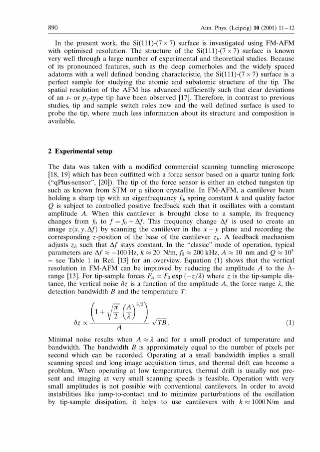
action, we assume that the induced charge is centered around the maximum of thecharge distribution at rmax ¼ 1:147�A with a radius s=2. Figure 8 shows the calcu-lated charge density. This figure shows, that in order to observe two separate max-ima of the charge density in an xy-plane, the z-distance of tip and sample atom
F. J. Giessibl et al., Imaging atomic orbitals with the Atomic Force Microscope 899
Fig. 8 Charge density (in electronsper �A3) for one 3sp3 orbital originat-ing from an adatom located at x ¼ 0and z ¼ 0 and two 3sp3 orbitals origi-nating from a tip atom located atx ¼ 0 and z ¼ 3:5�A. The mean den-sity of valence electrons in bulk sili-con is 0.2 electrons per �A3.
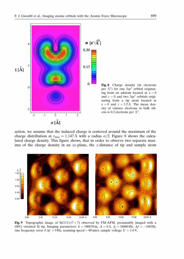
Fig. 9 Topographic image of Si(111)-(7� 7) observed by FM-AFM, presumably imaged with a(001) oriented Si tip. Imaging parameters: k ¼ 1800N/m, A ¼ 8�A, f0 ¼ 16860Hz, Df ¼ 160Hz,rms frequency error d Df ¼ 9Hz, scanning speed = 80 nm/s, sample voltage U ¼ 1:6V.

needs to be extremely small. Thus, imaging both dangling bonds separately is onlypossible if the minimal tip sample distance is of the order of the nearest neighbordistance of the atoms in the bulk crystal. The calculation of the charge densitydoes not take the interaction of the adatom and the tip into account. Because ofPauli’s exclusion principle, the adatom can only form a bond to one of the tipdangling bonds at the same time.The long-range forces described with the models above vary strongly with the
macroscopic tip shape, and the short-range forces are a function of the chemicalidentity of the front atom and its alignment to its bonding partners in the tip. Oncewe have learned to prepare the AFM tip in a well defined manner such that weknow the atomic arrangement and chemical identity of the tip apex, precise calcu-lations of the tip-sample force are highly desirable.
5 Experimental results and simulations
Figure 9 shows an experimental result of a Si(111)-(7� 7) surface observed by FM-AFM. Every adatom appears to have two peaks. This feature has been attributedto two dangling bonds originating at the tip which image the single dangling bondof the adatoms. While this image was recorded with a tungsten tip, we think thatthe tungsten tip had a silicon crystallite or cluster at its end. The notion, that tung-sten tips pick up silicon such that the front atom is made of silicon has been putforth in STM experiments before [41––43]. This interpretation of the data has beenchallenged recently [44]. We could show, that the feedback issues proposed are notrelevant in our experiment [45]. Further, the asymmetry between the two scandirections is not due to a finite feedback speed, but must be caused by elastic tipdeformations such as illustrated in Figure 10. Figure 11 shows a magnified view ofa single adatom. The distance between the contour lines is 10 pm, so the left peakis about 60 pm higher than the right peak and the depth between the peaks isapproximately 20 pm. Using Eq. 10, we can calculate the expected image once weknow the tip-sample force. As we have noted in Ref. [24], a qualitative picture canbe simulated from a long-range vdW force and a short range chemical force given
900 Ann. Phys. (Leipzig) 10 (2001) 11––12
Fig. 10 Tip bending effect: For a tip crystallite with the geometry proposed, the stiff-ness in scanning (x) direction is very small so it is likely that the tip apex bends oppositeto the scan direction. This bending explains the reversal in the height of the two adatompeaks when the scanning direction reverses (Fig. 9).

by the SW potential. Fig. 12 shows the result of that calculation. The left image issimulated for the experimental normalized frequency shift according to Figure 11where g ¼ 160Hz=16860Hz�1800N/m�ð8�AÞ3=2 ¼ 387 fNm1=2. The double
F. J. Giessibl et al., Imaging atomic orbitals with the Atomic Force Microscope 901
Fig. 11 Topographic image of a single adatom on Si(111)-(7� 7) observed by FM-AFM, presumably imaged with a (001) oriented Si tip. The following imaging param-eters were used: k ¼ 1800N/m, A ¼ 8�A, f0 ¼ 16860Hz, Df ¼ 160Hz, rms frequencyerror d Df ¼ 9Hz, scanning speed = 80 nm/s, sample voltage U ¼ 1:6V, scanning direc-tion: left to right.
Fig. 12. Simulation of a topographic FM-AFM image of a single adatom on Si(111)-(7� 7). Parameters (Left): g ¼ 387 fNm1=2, A ¼ 8�A, short-range force: Stillinger We-ber, tip geometry shown in Fig. 17, long-range force = 3:66� 1026 Jm/ðzþ DÞ2, D ¼ 5�A. Parameters (Right): g ¼ 4 fNm1=2, A ¼ 8�A, short-range force: Stillinger Weber, tipgeometry shown in Fig. 17, long-range force = 3:66� 1028 Jm/ðzþ DÞ2, D ¼ 5 �A.
peaked adatom image can only occur if the long-range attractive force is strongenough such that gmin occurs at a distance where the charge density of the tipshows strong lateral variations. The right image is simulated for g ¼ 4 fNm1=2 –– atypical value for weak vdW attractive forces [35, 36]. The left and the right imagesare simulated with a Si tip which exposes two dangling bonds (see Fig. 17). How-ever, the two dangling bonds appear separated only if the long-range attractiveforce is strong enough to allow imaging at very small distances. Several approxi-mate procedures for obtaining gðx; y; zÞ which are numerically much less expensivethan the exact calculation after Eq. (10) have been proposed:
1. Ke et al. [46] found that under certain conditions, the geometric mean betweenforce and energy is roughly proportional to the frequency shift;
2. Schwarz et al. [47] propose to approximate g by g �ffiffi2
p
pVtsffiffi
lp where l is the range
of the tip sample potential Vts;3. In an earlier publication [26] we proposed to decompose the tip-sample interac-
tion into monotonic basic types Fits with an exponential-, power- or inversepower- z-dependence and showed that g � 1ffiffiffiffi
2pp
PiFits
ffiffiffiffiffiffiffiffiffiffiffiffiffiffiVits=F
its
p.
However, as pointed out by Holscher et al. [48], the use of the approximativeapproaches leads to inaccuracies for small tip-sample distances. Moreover, method1 predicts that gðxÞ ¼ 0 for VtsðxÞ ¼ 0 and FtsðxÞ ¼ 0 and method 2 predicts thatgðxÞ ¼ 0 for VtsðxÞ ¼ 0 which is incorrect. Because we are simulating images atvery small tip-sample distances we refrain from using the approximate proceduresand perform the integration of g after Eq. (10). The integration is implementedwith Newton’s method –– a step width of 5 pm has proven to provide sufficientaccuracy.Qualitatively, the calculated image in Fig. 12 (left) is similar to the experimental
image in Fig. 11. However, the adatom height in the calculated image is only0.12�A –– a tenth of the experimental height. This is because the electrostatic shortrange interaction has been neglected. The relevance of the electrostatic short-rangeforce is confirmed by experimental results of atomic resolution on silicon with anapplied bias voltage where the normalized frequency shift has reached magnitudesas high as 180 fNm1=2 [23] and even 500 fNm1=2 [49].In Figure 13, we have also taken the short-range electrostatic force into account.
Because we have approximated the charges of the dangling bonds to concentrateon a point, the simulated adatom image shows two spherical subpeaks –– in con-trast to the crescent shaped experimental subpeaks. We expect that if accuratecharge distributions were taken into account, crescent shaped simulated imageswould result. The height of the simulated adatoms, the distance of the subpeaksand the dip between the subpeaks is in excellent agreement with the experimentalimages.Since our first observation of subatomic features by AFM, we have observed
similar images of double peaked adatom structures in various other experiments.In our first experiments, the orientation of the double peaks was roughly perpendi-cular to the fast scanning direction. In Figure 14 we present examples of AFMdata where the orientation of the crescents is clearly unrelated to the fast scanningdirection.
902 Ann. Phys. (Leipzig) 10 (2001) 11––12

Because of the dramatic dependence of the images on the atomic tip state, thepreparation of AFM tips with a specified front atom symmetry and chemical iden-tity is instrumental for performing well defined experiments. Commercial siliconcantilever tips are oriented in a (001)-direction. In silicon, the natural cleavageplanes are (111) planes. If a macroscopic tip crystallite is limited by natural clea-vage planes, a (001) oriented tip will in general not end in a single atom tip, but in
F. J. Giessibl et al., Imaging atomic orbitals with the Atomic Force Microscope 903
Fig. 13 Simulation of a topographicFM-AFM image of a single adatom onSi(111)-(7� 7). Parameters:g ¼ 387 fNm1=2, A ¼ 8�A, U ¼ 1:6V,short-range electrostatic force after Eq.21, tip radius R ¼ 1000�A, Hamaker con-stant AH ¼ 0:4 aJ, van der Waals force =AH � R=ð6ðzþ DÞ2Þ, D ¼ 2�A, long-range electrostatic force= U2pE0R=ðzþ D sÞ.
Fig. 14. Experimental FM-AFM images of adatoms exposing two peaks per atom. In allthe images, the fast scanning direction is horizontal (x). The orientation of the doublepeaks is clearly unrelated to the fast scanning direction.

a rooftop type of symmetry. A tip which points into a (111)-direction, however,will end in a single atom if we assume bulk termination. Moreover, the front atomof this tip is expected to be particularly stable, because it is bonded to the rest ofthe tip by three bonds and exposes a single dangling bond towards the sample.Because of this prospects, we have attempted to cleave single crystalline siliconsuch that we obtained crystallites which were limited by (111) planes supposedlyending in a single atom tip [50]. We have cleaved the silicon in air, so that anoxide layer of a typical thickness of 20�A will develop at the surface. As expected,the tips did not yield good STM images after bringing them into vacuum. How-ever, after exposing them to electron bombardment (the same procedure is usedfor preparing the silicon 7� 7 surface), the tips work excellently in STM mode andalso in AFM mode. We speculate, that the (111) oriented sidewalls of the tip willreconstruct just like a flat silicon surface. Even then, the front atom will be bondedto three next neighbors and expose a single dangling bond. Figure 15 shows anAFM image obtained with such a (111) oriented tip. It is also noted, that thisimage was recorded at positive frequency shift. Hence, the forces between frontatom and sample have been repulsive! An advantage of this mode is that the feed-back can be set much faster, because the risk of feedback oscillations with a cata-strophic tip crash is avoided in this mode. Due to the faster feedback setting and
904 Ann. Phys. (Leipzig) 10 (2001) 11––12
Fig. 15 Topographic image of Si(111)-(7� 7) observed by FM-AFM, imaged with a sin-gle crystal silicon tip roughly oriented in a (111) direction. Imaging parameters:k ¼ 1800N/m, A ¼ 2:5�A, f0 ¼ 20531Hz, Df ¼ þ85Hz, thus g ¼ þ30 fNm1=2, rms fre-quency error d Df ¼ 0:09Hz, scanning speed = 20 nm/s. The blue bars at the left andbottom border of the image indicate the x; y-range that is simulated in Fig. 16.
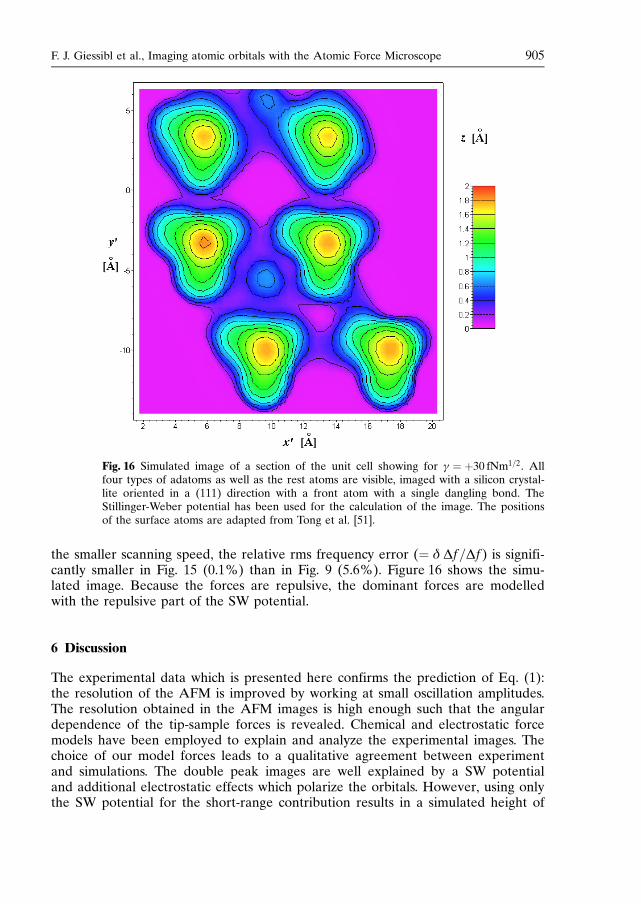
the smaller scanning speed, the relative rms frequency error (¼ d Df=Df ) is signifi-cantly smaller in Fig. 15 (0.1%) than in Fig. 9 (5.6%). Figure 16 shows the simu-lated image. Because the forces are repulsive, the dominant forces are modelledwith the repulsive part of the SW potential.
6 Discussion
The experimental data which is presented here confirms the prediction of Eq. (1):the resolution of the AFM is improved by working at small oscillation amplitudes.The resolution obtained in the AFM images is high enough such that the angulardependence of the tip-sample forces is revealed. Chemical and electrostatic forcemodels have been employed to explain and analyze the experimental images. Thechoice of our model forces leads to a qualitative agreement between experimentand simulations. The double peak images are well explained by a SW potentialand additional electrostatic effects which polarize the orbitals. However, using onlythe SW potential for the short-range contribution results in a simulated height of
F. J. Giessibl et al., Imaging atomic orbitals with the Atomic Force Microscope 905
Fig. 16 Simulated image of a section of the unit cell showing for g ¼ þ30 fNm1=2. Allfour types of adatoms as well as the rest atoms are visible, imaged with a silicon crystal-lite oriented in a (111) direction with a front atom with a single dangling bond. TheStillinger-Weber potential has been used for the calculation of the image. The positionsof the surface atoms are adapted from Tong et al. [51].

the adatoms which is only 10% of the experimental value. Adding the simple elec-trostatic short-range interaction, the height of the simulated adatoms agrees wellwith experiment, while the shape of the adatom images differs from experiment.The experimental images show crescents, while the theoretical images are spheri-cal. It is apparent that the simulation of the images captures the basic principle,but needs to be refined for obtaining a better agreement with experiment.The simulations covering the repulsive regime with a SW potential leads to a
qualitative agreement between experiment and simulations. The simulation showsthat the rest atoms, located between a corner adatom and two center adatoms,should be visible as a small protrusion. The experiment shows a saddlepoint at theexpected rest atom positions and a hole between three center adatoms. However,the shape of the four types of adatoms is similar in the simulation and very differ-ent in the experiment which shows that taking only next neighbor interaction andbond angles into account is insufficient for a proper model of the forces betweensilicon atoms. Also, the heights of the adatoms is much different than measured byLEED or predicted by calculations [52]. According to LEED data, the corner ad-atoms are only about 0.04�A higher than the center adatoms. In our AFM data, thecorner adatoms appear to be roughly 0.2 �A higher than the center adatoms. Be-cause this height difference is measured both with repulsive and attractive short-range forces, it cannot be caused by elastic deformations of tip and sample.Our simulations have shown, that the observation of atomic orbitals is only pos-
sible if the tip-sample distance is of the order of the interatomic distance in thebulk material. The forces that act for such small distances are large, and deforma-tions and increased dissipation are expected to occur. These issues and the observ-ability of atomic orbitals by STM are discussed in the following subsections.
6.1 Tip stability issues
An important issue arises in the tip and sample stability. So far, we have assumedthat both tip and sample atoms are not strained when the tip comes close to thesample. In STM, this might be the case when the tunneling impedance is large, andeven in dynamic AFM it is conceivable that Fts is small enough such that the elas-tic deformation of tip and sample is not noticeable.However, as is evident from Fig. 8, the observation of deviations of the spherical
symmetry of atoms is only possible in the near field, i.e. for distances which are ofthe order of the bulk interatomic distance. Thus, for observing these features byAFM, tip and sample have to come very close, and the atoms close to the interac-tion region will suffer from noticeable strain. Figure 17 shows a ball and stickmodel of a silicon crystallite which is limited by (111) planes and points into a(001) direction. This crystallite is used as a model for our tip.The stiffness of the bonds of the front atom to the upper part of the tip can be
estimated using the Stillinger-Weber potential. For the crystallite shown in Fig. 17,the stiffness in z-direction is 115N/m, in x-direction it is 20.4N/m and in y-direc-tion it is 224N/m. The stiffness can also be evaluated from the phonon spectrum ofsilicon. For an optical phonon at the G-point (i.e. the wave vector is zero), neigh-boring atoms vibrate opposite to each other. We can model this situation with asingle silicon atom which is suspended by four springs with half the length of the
906 Ann. Phys. (Leipzig) 10 (2001) 11––12

nearest neighbor distance, each having an effective spring constant in z-directionof kzhalf bond: The wave number of optical phonons in silicon at the G-point is520 cm1 which corresponds to fopt: phonon � 15:589THz [2]. The mean atomic mass(natural mixture of isotopes) of silicon is 28.086 amu [51], thus the spring constantkzhalf bond ¼ 1
4�447.45N/m = 111.9N/m. The stiffness of the two bonds connecting thefront atom of the tip crystallite with the rest of the tip is given by twice the stiffnessof one full-length bond with k ¼ 1
2 kz half bond yielding kz ¼ 111:9 N/m –– in excellentagreement with the value of 115N/m derived from the Stillinger-Weber potential.The positions of the two atoms which attach to the front atom have been kept
fixed for the derivations. In reality, all the tip atoms will respond to the force onthe front atom. The effect can be estimated by arranging the springs correspondingto a tip atom layer in series. For the tip shown in Fig. 17, the m-th bilayer containsone layer with m2 and one layer with mðmþ 1Þ atoms. Each of these atoms hastwo bonds to the layer above. The effective stiffness of the tip crystallite in z-direc-tion is then given by
1keff
¼ 1kz
P1m¼1
1m2
þ 1mðmþ 1Þ
� �¼ 1kz
1þ p2
6
� �� 1
0:4 � kz: ð26Þ
For tip-sample forces of the order of 2 nN, we expect that the bonds between thefront atom of the tip and its next neighbors will be strained by 2 nN=kz � 0:2�A.The total strain of the tip is expected to be 2 nN=kz=0:4 � 0:5�A. It is expected thatthe sample will become strained to a similar extent.
6.2 Amplitude feedback stability
When the oscillating cantilever of an FM-AFM comes close to the sample, in-creased damping has been observed experimentally [49, 53––55] and described the-oretically [13, 27, 56––59].We expect that in addition to the damping channels which are present in classic
FM-AFM, an even more significant damping channel will open up for very smalltip sample distances. When the front atom of the tip moves to the sample, both thefront atom and the adjacent sample atom will be pulled from their equilibriumposition and relax when the cantilever swings back from the sample. This processwill happen adiabatically and dissipate little energy as long as the closest distanceis larger than the distance where the maximal attractive force Fattmax occurs (in-flection point).
F. J. Giessibl et al., Imaging atomic orbitals with the Atomic Force Microscope 907
Fig. 17 Model for a tip crystallite cleaved frombulk silicon with (111)-oriented surfaces andpointing in a (001) direction.

However, when the distance between front atom and sample gets closer than theinflection point, an additional channel of significant energy loss will occur becausethe front atom of the tip and the sample atom will be pulled out of the equilibriumposition, and rather than moving back adiabatically, will stick together until thebonding force is overcome by the withdrawing cantilever. At this point, the frontatom and the sample atom will be pulled out by a distance Fattmax=kz. When thecantilever swings back, the front and sample atom will oscillate at the phononfrequency and dissipate the stored energy
DE ¼ F2attmax
2 kz: ð27Þ
Recently, a similar dissipation process has been described by Sasaki and Tsukada[59]. The maximal attractive force Fattmax is about 4 nN, according to the SW po-tential. Thus, the energy loss per cycle due to this process is 0.08 aJ per atom.Because both the front atom at the tip and the sample atom will be excited by thisprocess, the total energy loss is thus of the order of 1 eV per cycle. This energy hasto be provided by the oscillator circuit which drives the cantilever. The intrinsicenergy loss of the cantilever is pkA2=Q, where k is the spring constant of thecantilever, A is its oscillation amplitude and Q is its quality factor. For the qPlussensor, Q � 4000 and k ¼ 1800N/m. For an amplitude of the order of 1 nm, theintrinsic loss per cycle is of the order of 10 eV and the extra loss due to tip-sampledissipation is small. With conventional silicon cantilevers, typical Q factors are atleast one order of magnitude larger and the intrinsic dissipation is much smaller.Amplitude control can become difficult with conventional cantilevers when at-tempting to get very close to the sample as required for observing the orbital struc-ture of atoms.
6.3 Observability of individual orbitals by STM
To our knowledge, the observation of multiple maxima in the image of a singleatom in STM mode has not been reported before. We can identify three possibleexplanations why the internal orbital electron structure of atoms is observable byAFM, but apparently not by STM:
1. As shown in Fig. 8, the tip sample distance needs to be very small before thecharge density of valence electrons displays a noticeable deviation from the ro-tational symmetry about the z-axis. Typical tip-sample distances (from the cen-ter of the tip atom to the center of the closest sample atom) are 5––8�A in STM.When attempting to image in STM mode at a tip sample distance of 2––3�A, thetip-sample force is very large and the tip atom or sample atom may not with-stand the shear forces acting during scanning. In dynamic AFM, this small dis-tance occurs only intermittently and the lateral movement can occur during theoscillation phase where the tip is far from the sample;
2. While it is known that the force between two atoms is in general attractive atlarge distances and becomes repulsive at short distances, the tunneling currentis usually assumed to be a monotonic function of the distance. Thus, it is ex-pected that the orbital structure of the valence electrons has a larger effect onthe force than on the tunneling current;
908 Ann. Phys. (Leipzig) 10 (2001) 11––12
3. In the STM mode, typical tunneling voltages used for imaging silicon are of theorder of 2V and the energy of the tip and sample states which contribute to thetunneling current is spread over a range of 2 eV. Just like in atomic wave func-tions, where the angular dependent p; d and f sub-shells add up to a sphericallysymmetric charge distribution if all the states of a given main quantum numberare filled, we expect that a similar process can happen in tunneling experimentswhen a range of tip and sample energies contributes to the total tunneling cur-rent. So it is conceivable that even if some states which contribute to tunnelingare not symmetric with respect to the z-axis, the sum of these states is sym-metric around z.
In summary, we have shown that atomic force microscopy offers new insightsinto the atomic structure and symmetry of surface atoms and AFM tips. We areconfident that using small oscillation amplitudes, stiff cantilevers and oscillator set-ups which are insensitive to the enhanced damping at very close tip-sample dis-tances provides a new experimental tool to study the nature of the atomic bondand the electronic structure of atoms.
The authors wish to thank M. Herz, H. J. Hug, T. Kopp, M. Lantz, and C. Laschinger for fruitfuldiscussions. This work is supported by the BMBF (project no. 13N6918/1).
References
[1] R. E. Schlier and H. E. Farnsworth, J. Chem. Phys. 30 (1959) 917[2] Landolt-Bornstein, p. 370, Numerical Data and Functional Relationships in Science and Tech-
nology, Vol. 17a, edited by O. Madelung, M. Schultz, and H. Weiss, Springer, Berlin 1982[3] G. Binnig, H. Rohrer, Ch. Gerber, and E. Weibel, Phys. Rev. Lett. 50 (1983) 120[4] K. Takayanagi, Y. Tanishiro, and S. Takahashi, J. Vac. Sci. Technol. A 3 (1985) 1502[5] G. Binnig, C. F. Quate, and Ch. Gerber, Phys. Rev. Lett. 56 (1986) 930[6] L. Howald, R. Luthi, E. Meyer, and H.-J. Guntherodt, Phys. Rev. B 51 (1995) 5484[7] F. J. Giessibl, Science 267 (1995) 68[8] S. Kitamura and M. Iwatsuki, Jpn. J. Appl. Phys. 34 (1995) L145[9] Proceedings of the First International Workshop on Non-contact Atomic Force Microscopy
(Osaka, July 21––23, 1998, edited by S. Morita and M. Tsukada) Appl. Surf. Sci. 140 (1999)243––456
[10] Proceedings of the Second International Workshop on Non-contact Atomic Force Microscopy(Pontresina, September 1––4, 1999, edited by R. Bennewitz, Ch. Gerber, and E. Meyer) Appl.Surf. Sci. 157 (2000) 207––428
[11] Proceedings of the Third International Conference on Non-contact Atomic Force Microscopy(Hamburg, July 16––19, 2000, edited by U. D. Schwarz, H. Holscher, and R. Wiesendanger)Appl. Phys. A 72 (2001) S1-S141
[12] T. R. Albrecht, P. Grutter, D. Horne, and D. Rugar, J. Appl. Phys. 69 (1991) 668[13] F. J. Giessibl, H. Bielefeldt, S. Hembacher, and J. Mannhart, Appl. Surf. Sci. 140 (1999) 352[14] R. Perez, I. Stich, M. C. Payne, and K. Terakura, Phys. Rev. Lett. 78 (1997) 678[15] R. Perez, I. Stich, M. C. Payne, and K. Terakura, Phys. Rev. B 58 (1998) 10835[16] K. D. Brommer, B. E. Larson, M. Needels, and J. D. Joannopoulos, Jpn. J. Appl. Phys. 32
(1993) 1360[17] F. J. Giessibl, S. Hembacher, H. Bielefeldt, and J. Mannhart, Science 289 (2000) 422[18] ThermoMicroscopes Inc., 1171 Borregas Ave., Sunnyvale, CA 94089, USA[19] F. J. Giessibl and B. M. Trafas, Rev. Sci. Instrum. 65 (1994) 1923
F. J. Giessibl et al., Imaging atomic orbitals with the Atomic Force Microscope 909
[20] F. J. Giessibl, Appl. Phys. Lett. 76 (2000) 1470[21] F. J. Giessibl, Habilitation thesis, Augsburg University 2000[22] Nanosurf AG, 4410 Liestal, Switzerland[23] R. Luthi, E. Meyer, M. Bammerlin, A. Baratoff, T. Lehmann, L. Howald, Ch. Gerber, and
H.-J. Guntherodt, Z. Phys. B 100 (1996) 165[24] F. J. Giessibl, Phys. Rev. B 56 (1997) 16010[25] F. J. Giessibl, Appl. Phys. Lett. 78 (2001) 123[26] F. J. Giessibl and H. Bielefeldt, Phys. Rev. B 61 (2000) 9968[27] U. Durig, New Journal of Physics 2 (2000) 5.1[28] M. Z. Bazant, E. Kaxiras, and J. F. Justo, Phys. Rev. B 56 (1997) 8542[29] H. C. Hamaker, Physica 4 (1937) 1058[30] J. Israelachvili, Intermolecular and Surface Forces, 2nd ed., Academic Press, London 1991[31] T. J. Senden and C. J. Drummond, Colloids Surf. A 94 (1995) 29[32] H. Holscher, U. D. Schwarz, and R. Wiesendanger, Appl. Surf. Sci. 140 (1999) 344[33] F. H. Stillinger and T. A. Weber, Phys. Rev. B 31 (1985) 5262[34] F. F. Abraham, I. P. Batra, and S. Ciraci, Phys. Rev. Lett. 60 (1988) 1314[35] M. A. Lantz, H. J. Hug, P. J. A. van Schendel, R. Hoffmann, S. Martin, A. Baratoff, A. Abdur-
ixit, H.-J. Guntherodt, and Ch. Gerber, Phys. Rev. Lett. 84 (2000) 2642[36] M. A. Lantz, H. J. Hug, R. Hoffmann, P. J. A. van Schendel, P. Kappenberger, S. Martin,
A. Baratoff, and H.-J. G€untherodt, Science 291 (2001) 2580[37] C. Laschinger, diploma thesis, Augsburg University 2001[38] L. Olsson, N. Lin, V. Yakimov, and R. Erlandsson, J. Appl. Phys. 84 (1998) 668[39] R. P. Feynman, R. B. Leighton, and M. Sands, The Feynman Lectures on Physics , Vol. II,
chapters 6––7, Sixth Printing, Addison Wesley, Reading 1977[40] R. McWeeny, Coulson’s Valence, p. 42, Oxford University Press, Oxford 1991[41] J. E. Demuth, U. Kohler, and R. J. Hamers, J. Microsc. 151 (1988) 299[42] C. J. Chen, J. Vac. Sci. Technol. A 1 (1991) 44[43] C. J. Chen, Introduction to Scanning Tunneling Microscopy, p. 88, Oxford University Press
1993[44] H. J. Hug, M. A. Lantz, A. Abdurixit, P. J. A. van Schendel, R. Hoffmann, P. Kappenberger,
and A. Baratoff, Science 291 (2001) 2509a, online available at www.sciencemag.org/ cgi/ con-tent/ full/291/5513/2509a.
[45] F. J. Giessibl, S. Hembacher, H. Bielefeldt, and J. Mannhart, Science 291 (2001) 2509a, onlineavailable at www.sciencemag.org/ cgi/ content/ full/291/5513/2509a.
[46] S. H. Ke, T. Uda, and K. Terakura, Phys. Rev. B 59 (1999) 13267[47] U. D. Schwarz, H. Holscher, and R. Wiesendanger, Phys. Rev. B 62 (2000) 13089[48] H. Holscher, W. Allers, U. D. Schwarz, A. Schwarz, and R. Wiesendanger, Appl. Phys. A 72
(2001) S35[49] M. Guggisberg, M. Bammerlin, A. Baratoff, R. Luthi, Ch. Loppacher, F. M. Battiston, J. Lu,
R. Bennewitz, E. Meyer, and H.-J. Guntherodt, Surf. Sci. 461 (2000) 255[50] F. J. Giessibl, S. Hembacher, H. Bielefeldt, and J. Mannhart, Appl. Phys. A 72 (2001) S15[51] S. Y. Tong, H. Huang, C. M. Wei, W. E. Packard, F. K. Men, G. Glander, M. B. Webb, J. Vac.
Sci. Technol. A 6 (1988) 615[52] N. Ashcroft and N. D. Mermin, Solid State Physics, Saunders College, Philadelphia 1981[53] R. Luthi, E. Meyer, M. Bammerlin, A. Baratoff, L. Howald, Ch. Gerber, and H.-J. Guntherodt,
Surface Review and Letters 4 (1997) 1025[54] M. Bammerlin, R. Luthi, E. Meyer, A. Baratoff, J. Lu, M. Guggisberg, Ch. Gerber, L. Howald,
and H.-J. Guntherodt, Probe Microscopy 1 (1997) 3[55] H. Ueyama, Y. Sugawara, and S. Morita, Appl. Phys. A 66 (1998) S295[56] U. Durig, Surf. Interface Anal. 27 (1999) 467[57] M. Gauthier and M. Tsukada, Phys. Rev. Lett. 84 (1999) 2642; Phys. Rev. B 60 (1999) 11716[58] A. Abdurixit, A. Baratoff, and E. Meyer, Appl. Surf. Sci. 157 (2000) 355[59] N. Sasaki and M. Tsukada, Jpn. J. Appl. Phys. 39 Part 2 (2000) L1334
910 Ann. Phys. (Leipzig) 10 (2001) 11––12