Embed Size (px)
Citation preview

III. Sound EqualizerJorge D Morales
Fig. 1. Schematic View
Abstract—Signal processing is one of the most importantfeatures of electric circuits. It is the basis for electronics, sensing,triggering and acting to transform the physical principles ofelectricity into technology. This experiment will allow you tograsp some fundamental concepts on simple circuits and ACcurrent by implementing a set of filters and amplifiers to producea 2-band sound equalizer.
I. INTRODUCTION
In this experiment we will make a device which mainintention is to produce an arbitrary, and modifiableenhancement of the sound tone for an input signal (e.g.music). By splitting the audible frequencies into two bands(low and high), and implementing a control device to modifysuch intensities. To achieve this goal we will build a signalprocessor which tries to split the frequency spectra usinga Sallen-Key arrangement (of resistors, capacitors, andan operational amplifier). This device is a simple secondorder linear filter which permits to obstruct a frequency range.
Furthermore, the signal will be amplified with variableintensity so that the filtered frequencies are intensifiedor reduced, hence creating an enhancement of the desiredfrequency bands. By arranging two filters with their amplifiers,we could split the signal into two, compensating spectra,which after adding the signal back, will reproduce thearbitrary modifications of the amplitudes of the frequencybands over the original signal.
The system will essentially consist of two filters, twoamplifiers, and a signal summator. See Figure 1.
Naturally the functionality of this device relies on theResistor-Capacitor combination in an AC circuit. Includingalso an operational amplifier (opamp), device which mainpurpose is to increase or dreduce the input’s amplitude. Sothe RC design will regulate the frequency while the opamp,will modulate the intensity of the output.
Opamps were developed in the late 30’s to astelecommunications was barely arising. The signal on phonelandlines was weak, and needed constant re-amplification.The solutions given at that time made the signal get rapidlydistorted or still faint. Harry Black, came up with the firstopamp design, with the following idea: the amplifier createsan excess of amplification, then sends back to the circuitsome part of it (called a feedback) in a way that makes thecircuit gain dependent on the feedback circuit rather than theamplifier gain. In this way the circuit gain depends on thepassive feedback instead of the active amplifier [1]. Opampsproduce control systems which are self-regulating throughthe feedback impulse, which makes them fairly stable andsimple to use. The actual design of modern day opamps isachieved via transistors, diodes and such elements, but forthe purposes of this procedure will not be taken into account.Instead the opamp will be trated as a primary element, andits properties will be described to the necessary extent.
II. IMPLEMENTATION
A. RLC Circuits
Recall that resistor-inductor-capacitor circuits areoscillatory; they form a harmonic oscillator for currentand produce resonance at certain frequencies. The nature ofsuch oscillations may be inferred from the properties of theresistor, inductor, and capacitor.
The inductor and capacitor alone, produce resonancefor certain frequencies. Both elements have an impedance(resistance analogous) that oscillates along with the circuit, sofrequencies occurring when the impedance is at a minimumproduce resonance. The rest of them suffer distortion,although some modes may coincide with harmonics of theoriginal ’natural’ frequency.
The resistor simply acts as a damper. That is, it impedesthe signal to propagate freely, so that it decays. Resistorsare power dissipaters, so they get rid of the energy passingthrough the AC wave.
Recall the general equation for an RLC circuit, constructedfrom Kirchhoff’s voltage law:
d2i(t)
dt2+R
di(t)
dt+
1
LCi(t) = 0 (1)

Which may be rewritten with the following factors:
d2i(t)
dt2+ 2α
di(t)
dt+ ω
20i(t) = 0 (2)
Where α is the attenuation factor or neper frequency(coupled to the resistor), and ω0 is the angular frequencyrelated to the natural frequency of the system. The solutionto this equation is of the form ∼ e
st. Where s is a complexvariable precisely dependant on the α and ω0 variables.
s2 + 2α+ ω
20 = 0 (3)
The equation represents an oscillation that is attenuated forfrequencies outside of the natural frequency and its modes.Furthermore, the Laplace Domain under this variable providesan easy approach to certain characteristics, which will bedescribed afterwards.
B. Damping FactorThe solutions for the s variable produce two interesting
scenarios.
s = −α±α2 − ω
20 (4)
Where the turning point is given by the argument of thesquare root. A factor ζ is defined as the ratio of α over ω0.Which contain the information for such scenarios. ζ is namedthe damping factor.
Different kinds of systems may be defined through thisfactor:
• ζ > 1 Overdamped. The system returns in an exponentialdecay to its equilibrium without oscillation, the greaterthe slower it takes.
• ζ = 1 Critically Damped. The system returns to equilib-rium as quickly as possible, withot oscillating.
• 0 < ζ < 1 Underdamped. The system oscillates andgradually returns to the equilibrum state.
• ζ = 0 Undamped. Harmonic oscillation.Even more, an equivalent way of describing the system is
through the Q factor (Quality Factor). In this case the ratiois ω0/2α, which allows to draw the same conclusions butinstead with limits of 1/2, it also allows to understand theband response of different frequencies.
• Q = inf Undamped. The frequency band is narroweduntil only the natural frequency moves in harmonicoscillation.
• Q > 1/2 Underdamped. Oscillation at some frequenciesnear w0 that decay gradually. The lower, the broader.
• Q = 1/2 Critically Damped.• Q < 1/2 Overdamped.
C. Laplace DomainLaplace Transformations may be applied to linear systems,
to represent the input, output signal. The transformation isapplied to the differential equation, to change the secondorder dependence, to a linear dependence e.g.:
Y (s) = H(s)X(s) (5)
Then, H(s) is the transfer function that linearly relates theinput to the output:
H(s) =Y (s)
X(s)=
L (y(t))
L (x(t))(6)
In the case of a simple RLC circuit, the transformationmay be applied (or simply revising the net impedance of thecircuit and seting up Kirchhoff’s Law). The transformation inthis case yields:
V (s) = I(s)
R+ sL+
1
sC
(7)
If we identify I(s) to Y(s) and V(s) with X(s) then we candefine the transfer function for our circuit to be:
H(s) =s
Ls2 + R
L s+1
LC
(8)
The importance of this transformation is that we don’treally have to derive the solution of the particular differentialequation but rather, after identifying its nature we can inferthe characteristics and predict the values for the output.
D. OpampAs mentioned in the introduction, the internal configuration
of an operational amplifier and its full understanding will notbe covered in this project, but instead we will understandits operational features, and apply those rules to our knownKirchhoff Law to produce a high quality filter. Filters arein nature governed by RLC circuits but if an opamp is notincluded the response of the filter is more drastic and morebiased by the filter resonance with the input signal, hencecreating noise, especially with a signal that is not pure, but arather rapidly variable and oscillating intensity (like music).
Opamps consist of three active terminals (the ones whichwill actually carry the signal and modify it): v+, v−, vout.And two passive ends which are simply the opamp’s voltagesource: vcc+, vcc−. See Figure 2. Opamps require very littlecurrent to operate, nonetheless they do require a feedingvoltage.
The simplest opamp configuration, without a feedback,just receiving a signal in the v+ input. Grounded through a

Fig. 2. Opamp Schematic View
resistor in the v−, and sending the output without feedback,in principle merely amplifies the voltage difference of v+
and v−. It amplifies in a way proportional to the Amplifier’sOpen-Loop Gain. This is a specification particular of eachdevice, and is commonly in the order of 104. As mentioned,the purpose of the opamp is to work with a feedback,since it is such a feature that makes it special. The closed-loop configuration on the other hand (Figure ??) reducesdramatically the output gain, compensating the open-loop gain.
When working with a signal (generally with a feedbackconfiguration) the opamp keeps the input terminals withno voltage difference (v+ = v−), as the output terminalcompensates for that. This also requires that the inputterminals draw no current.
These simple set of rules turn the opamp into a black-boxwhich merely follows the following rule:
v+ = v− = vout (9)
And by applying Kirchhoff’s Law with these conditions,and obtaining the transfer function of vout/vin, andrecognizing the terms in such Laplace domain, allow us todesign a specific filter for specific frequencies and conditions.
The opamp, is also used with a final variation of thefeedback terminal, that is setting up a voltage divider to makea constant ’inner gain’. Such a configuration may be seenin Figure 3. And the output (hence a factor multiplying theoriginal transfer function is added.
By following Kirchhoff’s Law,
vout = v− + IRa (10)
where we know that I is equal to the current goingonly from v− to ground, passing through Rg , because theimpedance between v+ and v− should be so large thatno current flows through the opamp. Then, since Rg andRa are in an approximation to a series circuit, the current
Fig. 3. Inner Gain
flowing through them is the same, thus I = v−/Rg . We have,substituting back, and recognizing that the input voltages areequal:
vout = v+ + v+Ra
Rg= v+
1 +
Ra
Rg
(11)
Then the factor G, multiplies the transfer function Hwhenever such a configurtion is added. Making it simple todesign a filter with no inner-gain, and finally multiplyingsuch factor to the transfer function (within some correctionsdue to the circuit dependence):
G =vout
v+= 1 +
Ra
Rg(12)
E. 2 Band Signal Split
1) Sound Considerations - Music: The purpose of thisproject is to apply a configuration of RC circuits with anopamp to divide the signal into two channels, a low pass anda high pass. Then control the gain of the amplification ofeach channel independently to allow to choose the tone ofthe signal, and finally add back the signals together.
It is required to notice that the human ear is capable oflistening frequencies from 20Hz to 20kHz approximately.And that the pitch of notes has greater frequency steps inthe lower frequencies. So in this project we will require tosplit the filter’s bandwidth in two sectors, below 1.8kHz, andabove 2kHz. Leaving a 200Hz safe band gap between them.This gap is set to allow for underdamped frequencies of bothfilters to overlap without increasing strongly their amplitude.

Fig. 4. Filter Topology
2) Sallen-Key Topology: In this case, the filters have thefollowing topology (Figure 4). The only difference betweensetting a highpass or a lowpass filter is the in the orderof accommodating the capacitors and resistors of the activecomponents. The schematic view shows impedances which canbe substituted with the equivalent impedance of such devices.
At Vz we have the following equation:
Vin − Vz
Z1=
Vz − V+
Z2+
Vz − Vout
V4(13)
And given the opamp functionality, it becomes:
Vin − Vz
Z1=
Vz − Vout
Z2+
Vz − Vout
V4(14)
Furthermore, at v+, and replacing v+ with vout:
Vz − Vout
Z2=
Vout
Z3(15)
Finally, we obtain the equation:
Vz = Vout
1 +
Z2
Z3
(16)
Which yields at last:
Vout
Vin=
Z3Z4
Z1Z2 + Z4(Z1 + Z2) + Z3Z4≡ H(s) (17)
Which is in general the transfer function for our filter.
3) Low Pass Filter: The filter has a structure given byFigure 5. In this case the variables for H(s) take the followingform.
Z1 = R1 Z2 = R2 Z3 =1
sC1Z4 =
1
sC2(18)
Furthermore we will define our filter to be in a near criticallydamped state (i.e. Q=1/2). And Since there is no restrictionwe will allow the resistors and capacitors be equivalent to aninteger proportionality of each other (C1 = nC2, R1 = mR2).
Fig. 5. Low Pass Filter
We can recognize the following expression for the transferfunction (after substitution of previous expression of H(s)):
H(s) =1
C1C2R1R2
s2 + s
R1+R2C2R1R2
+ 1
C1C2R1R2
(19)
With this expression we an easily identify the naturalfrequency ω0, the quality factor Q, and the attenuationparameter α. Which are the essential equations for our filter.We realize that the system is overdetermined, so if we choosethe natural frequency, and the quality factor, we can stillimpose the proportionality conditions mentioned above.
ω20 =
1
C1C2R1R2(20)
2α =R1 +R2
C2R1R2(21)
Q =ω0
2α(22)
Imposing such conditions over the quality factor, we obtain:
Q =
√mn
1 +m= 1/2 (23)
Where we can easily identify that it is met when m=n=1.
Finally, we have come up with simple expressions (LettingR1 = R2 = R, and C1 = C2 = C):
ω0 =1
RC(24)
Which allows us to determine the value of one of thecomponents, after fixing a natural frequency. (and recallingthat ω0 = 2πf0) and f is the oscillation frequency (notangular frequency). Where in this case we want to set thisfilter to 1800Hz. And we are provided with capacitors of
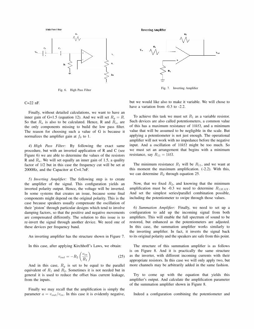
Fig. 6. High Pass Filter
C=22 nF.
Finally, without detailed calculations, we want to have aninner gain of G=1.5 (equation 12). And we will set Rg = R.So that Ra is also to be calculated. Hence, R and Ra, arethe only components missing to build the low pass filter.The reason for choosing such a value of G is because itnormalizes the amplifier gain at f0 to 1.
4) High Pass Filter: By following the exact sameprocedure, but with an inverted application of R and C (seeFigure 6) we are able to determine the values of the resistorsR and Ra. We will set equally an inner gain of 1.5, a qualityfactor of 1/2 but in this case the frequency cut will be set at2000Hz, and the Capacitor at C=4.7nF.
5) Inverting Amplifier: The following step is to createthe amplifier of the signal. This configuration yields aninverted polarity output. Hence, the voltage will be inverted.In some systems that creates an issue, because some finalcomponents might depend on the original polarity. This is thecase because speakers usually compensate the oscillation oftheir ’piston’ through particular designs which tend to involvedamping factors, so that the positive and negative movementsare compensated differently. The solution to this issue is tore-invert the signal through another device. We need one ofthese devices per frequency band.
An inverting amplifier has the structure shown in Figure 7.
In this case, after applying Kirchhoff’s Laws, we obtain:
vout = −R2
vin
R1
(25)
And in this case, Rg is set to be equal to the parallelequivalent of R1 and R2. Sometimes it is not needed but ingeneral it is used to reduce the offset bias current leakage,from the inputs.
Finally we may recall that the amplification is simply theparameter a = vout/vin. In this case it is evidently negative,
Fig. 7. Inverting Amplifier
but we would like also to make it variable. We will chose tohave a variation from -0.3 to -2.2.
To achieve this task we must set R1 as a variable resistor.Such devices are also called potentiometers, a common valueof this has a maximum resistance of 10kΩ, and a minimumvalue that will be assumed to be negligible in the scale. Butapplying a potentiometer is not just enough. The operationalamplifier will not work with no impedance before the negativeinput. And a oscillation of 10kΩ might be too much. Sowe must set an arrangement that begins with a minimumresistance, say R11 = 1kΩ.
The minimum resistance R1 will be R11, and we want atthis moment the maximum amplification. (-2.2). With this,we can determine R2 through equation 25.
Now, that we fixed R2, and knowing that the minimumamplification must be -0.3 we need to determine R1MAX .And set the simplest series/parallel combination possible,including the potentiometer to swipe through those values.
6) Summation Amplifier: Finally, we need to set up aconfiguration to add up the incoming signal from bothamplifiers. This will enable the full spectrum of sound to berestored, but enhanced as the potentiometers are adjusted.In this case, the summation amplifier works similarly tothe inverting amplifier. In fact, it inverts the signal backto its original polarity and the speakers are safe from this point.
The structure of this summation amplifier is as followsis on Figure 8. And it is practically the same structureas the inverter, with different incoming currents with theirappropriate resistors. In this case we will only apply two, butmore channels may be arbitrarily added in the same fashion.
Try to come up with the equation that yields thisamplifier’s output. And calculate the amplification parameterof the summation amplifier shown in Figure 8.
Indeed a configuration combining the potentiometer and
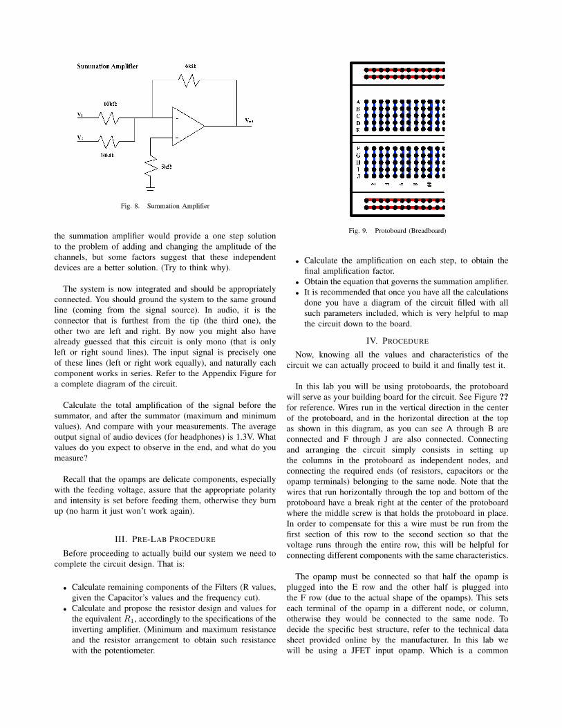
Fig. 8. Summation Amplifier
the summation amplifier would provide a one step solutionto the problem of adding and changing the amplitude of thechannels, but some factors suggest that these independentdevices are a better solution. (Try to think why).
The system is now integrated and should be appropriatelyconnected. You should ground the system to the same groundline (coming from the signal source). In audio, it is theconnector that is furthest from the tip (the third one), theother two are left and right. By now you might also havealready guessed that this circuit is only mono (that is onlyleft or right sound lines). The input signal is precisely oneof these lines (left or right work equally), and naturally eachcomponent works in series. Refer to the Appendix Figure fora complete diagram of the circuit.
Calculate the total amplification of the signal before thesummator, and after the summator (maximum and minimumvalues). And compare with your measurements. The averageoutput signal of audio devices (for headphones) is 1.3V. Whatvalues do you expect to observe in the end, and what do youmeasure?
Recall that the opamps are delicate components, especiallywith the feeding voltage, assure that the appropriate polarityand intensity is set before feeding them, otherwise they burnup (no harm it just won’t work again).
III. PRE-LAB PROCEDURE
Before proceeding to actually build our system we need tocomplete the circuit design. That is:
• Calculate remaining components of the Filters (R values,given the Capacitor’s values and the frequency cut).
• Calculate and propose the resistor design and values forthe equivalent R1, accordingly to the specifications of theinverting amplifier. (Minimum and maximum resistanceand the resistor arrangement to obtain such resistancewith the potentiometer.
Fig. 9. Protoboard (Breadboard)
• Calculate the amplification on each step, to obtain thefinal amplification factor.
• Obtain the equation that governs the summation amplifier.• It is recommended that once you have all the calculations
done you have a diagram of the circuit filled with allsuch parameters included, which is very helpful to mapthe circuit down to the board.
IV. PROCEDURE
Now, knowing all the values and characteristics of thecircuit we can actually proceed to build it and finally test it.
In this lab you will be using protoboards, the protoboardwill serve as your building board for the circuit. See Figure ??for reference. Wires run in the vertical direction in the centerof the protoboard, and in the horizontal direction at the topas shown in this diagram, as you can see A through B areconnected and F through J are also connected. Connectingand arranging the circuit simply consists in setting upthe columns in the protoboard as independent nodes, andconnecting the required ends (of resistors, capacitors or theopamp terminals) belonging to the same node. Note that thewires that run horizontally through the top and bottom of theprotoboard have a break right at the center of the protoboardwhere the middle screw is that holds the protoboard in place.In order to compensate for this a wire must be run from thefirst section of this row to the second section so that thevoltage runs through the entire row, this will be helpful forconnecting different components with the same characteristics.
The opamp must be connected so that half the opamp isplugged into the E row and the other half is plugged intothe F row (due to the actual shape of the opamps). This setseach terminal of the opamp in a different node, or column,otherwise they would be connected to the same node. Todecide the specific best structure, refer to the technical datasheet provided online by the manufacturer. In this lab wewill be using a JFET input opamp. Which is a common

Fig. 10. UA 741
Fig. 11. UA 741 Pins
device used for the kind of sensitivity, distortion and voltageparameters we need (i.e. Iexas Instruments TL082, or STUA741), although a general purpose operational amplifierworks, as long as it is sensitive enough, and the input admitsnegative impulse (i.e. at least ±3V ).
Figure ?? and 11 provide the conceptual view of an opamp(ST UA741), and the map for connecting the pins. Takenfrom the manufacturer’s datasheet [3].
The opamps work with an input voltage in the 30V range,that is the vcc inputs of the opamp (which naturally don’tact on the signal circuit, but just on the opamp feed) are tobe provided by a DC source, set up on the manufacturer’sspecified voltage difference. Warning, this is the most delicatepart, connecting the feed voltage improperly or inversely willburn the opamp and waste it. So before turning the voltagesource on, make sure to verify the feed is set up properly. TheDC supplier works as a battery with a predefined voltage ifthe voltage is not enough, connect several in series, to add thevoltage, they restrict due to safety issues the current output,but the opamps are supposed to function with neglectiblecurrent.
We will also be using a Frequency generator see Figure 12,the frequency generator can be connected to the circuit, itoutputs different frequencies and functions which can beseen if the circuit is then attached to a oscilloscope, whichis another item we will be using to test the circuit. Use thefunction generator, to observe the response of the filter to thedifferent frequencies. Set the frequency in different ranges,and then proceed to compare the signal amplitude before andafter the components we are building. Plug the Hi Lo outputterminals to the ground and input terminals of our design.(Don’t confuse the ground with the negative feed vcc they are
Fig. 12. Frequency Generator
Fig. 13. Old Oscilloscope
independent, the feed is not counted in the circuit’s diagram,but only in the connection of the opamps).
A. Test with Oscilloscope
Then we shall use the oscilloscope to actually see thesignal. The oscilloscope basically takes voltage amplitudereadings which are then displayed on a graph (V vs time).See Figures 13. and 14 for a reference of two kinds ofoscilloscopes (digital and analogical). An oscilloscopeconnector is plugged in through the coaxial cable, and sinceit is used to read the signal, should be grounded to thecircuit’s ground, and the active input positioned at the nodein which the oscillation is read. It is recommended to usea two channel oscilloscope to compare both signals at thesame time. (input and output signals). That way you canverify what the circuit is doing and test every part of thecircuit while you have an input, and find the non working ormalfunctioning elements if they exist.
B. Test with Music
Once the filters are tested with the function generator,music may be connected. If done properly there is nofeedback on the input terminals so the connected device issafe, actually this is protected by the opamp configuration.Connect music and observe the variation of the signal withthe oscilloscope. The last part needed is some speakers. Once

Fig. 14. New Oscilloscope
the system is proved to be working without inverting thepolarity, and in the amplitude range desired, you may connectthe speakers, in the same way as the oscilloscope, groundingto the circuit’s ground, and transferring the output to one ofthe left-right channels.
1) Step Enumeration:1) This lab will be done in teams, each creating a small set
of the components.2) Assemble the filter. Make sure to connect each wire
to the correct location on the op-amp. Test with thefunction generator and the oscilloscope. Remember toground the circuit to the dame node, but that the neg-ative input voltage vcc of the opamp is not. Measurethe amplification, at different frequencies, including thenatural frequency.
3) Build the inverting amplifier, using the potentiometerlocated in the breadboard, test this component withdifferent frequencies and measure the amplification.
4) Connect the output of the filter to the input of theinverting amplifier. Also connect grounds and inputvoltages. Measure the combined amplification.
5) Match with another team compensating for the band-width of your device.
6) Next construct the summation amplifier on its ownprotoboard, (remember this gadget should revert thepolarity) as it combines and inverts the signal back to thecorrect polarity, make sure that is happening. Measurethe amplification factor of this device independently, andthen the amplification of the whole system (at differentfrequencies).
7) Now that the equalizer is finished we can begin testingit with music.
8) You must then connect an auxiliary cord to the inputand connect both filters to create a common node. Andnaturally, grounding the system to the chord’s groundline.
9) Finally attach your equalizer to the speakers and youcan begin playing music.
10) Vary the resistance in both the high and low pass filterand observe the results.
V. ACKNOWLEDGEMENTS
This lab was done with greatly appreciated help frommy friend Santiago Torres, guiding me to the necessary
understanding of signal filters. His comments, referencesand suggestions have made this lab possible, and hopefullyattractive.
I also want to thank my student Brian James Quina, whohas helped me in the documentation and also through valuableinput to make this lab better adapted and interesting.
REFERENCES
[1] Carter, Bruce, etal. Opamps for Everyone. Second Edition, TexasInstruments, MA 2003.
[2] Texas Instruments. TL081,2,3,4 Datasheet. TX 2013.http://www.ti.com/lit/ds/symlink/tl084.pdf
[3] ST Microelectronics. UA741 Datasheet. Italy, 2001.http://www.datasheetcatalog.org/datasheet/stmicroelectronics/5304.pdf