Embed Size (px)
Citation preview

This article has been accepted for inclusion in a future issue of this journal. Content is final as presented, with the exception of pagination.
IEEE TRANSACTIONS ON ELECTRON DEVICES 1
Current Status and Opportunities of OrganicThin-Film Transistor Technologies
Xiaojun Guo, Member, IEEE, Yong Xu, Member, IEEE, Simon Ogier, Tse Nga Ng, Mario Caironi,Andrea Perinot, Ling Li, Jiaqing Zhao, Wei Tang, Radu A. Sporea, Member, IEEE,
Ahmed Nejim, Jordi Carrabina, Paul Cain, and Feng Yan
Abstract— Attributed to its advantages of super mechan-ical flexibility, very low-temperature processing, and com-patibility with low cost and high throughput manufacturing,organic thin-film transistor (OTFT) technology is able tobring electrical, mechanical, and industrial benefits to awide range of new applications by activating nonflat sur-faces with flexible displays, sensors, and other electronicfunctions. Despite both strong application demand andthese significant technological advances, there is still a gapto be filled for OTFT technology to be widely commerciallyadopted. This paper provides a comprehensive review of thecurrent status of OTFT technologies ranging from material,device, process, and integration, to design and systemapplications, and clarifies the real challenges behind to beaddressed.
Index Terms— Displays, flexible electronics, hybrid inte-gration, organic thin-film transistor (OTFT), printed electron-ics, sensors.
Manuscript received December 17, 2016; revised February 7, 2017;accepted February 18, 2017. This work was supported in part bythe National Key Research and Development Program of “StrategicAdvanced Electronic Materials” under Grant 2016YFB0401100 and inpart by the NSFC of China under Grant 61274083 and Grant 61334008.The review of this paper was arranged by Editor Y.-Y. Noh.
X. Guo, J. Zhao, and W. Tang are with the National Engineering Labora-tory of TFT-LCD Materials and Technologies, Department of ElectronicEngineering, Shanghai Jiao Tong University, Shanghai 200240, China(e-mail: [email protected]).
Y. Xu is with the Department of Energy and Materials Engi-neering, Dongguk University, Seoul 100-715, South Korea (e-mail:[email protected]).
S. Ogier is with NeuDrive Ltd, Macclesfield SK10 4TG, U.K. (e-mail:[email protected]).
T. N. Ng is with the Department of Electrical and Computer Engi-neering, University of California, San Diego, CA 92093 USA (e-mail:[email protected]).
M. Caironi and A. Perinot are with the Cen-ter for Nano Science and Technology@PoliMi, Isti-tuto Italiano di Technologia, 20133 Milan, Italy (e-mail:[email protected]; [email protected]).
L. Li is with the Institute of Microelectronics, Chinese Academy ofSciences, Beijing 100029, China (e-mail: [email protected]).
R. A. Sporea is with the Advanced Technology Institute, University ofSurrey, Guildford GU2 7XH, U.K. (e-mail: [email protected]).
A. Nejim is with Silvaco Europe Ltd, Cambridgeshire PE27 5JL, U.K.(e-mail: [email protected]).
J. Carrabina is with the Autonomous University of Barcelona,08192 Bellaterra, Spain (e-mail: [email protected]).
P. Cain is with FlexEnable Ltd., Cambridge CB4 0FX, U.K. (e-mail:[email protected]).
F. Yan is with the Department of Applied Physics and MaterialsResearch Center, The Hong Kong Polytechnic University, Hong Kong(e-mail: [email protected]).
Color versions of one or more of the figures in this paper are availableonline at http://ieeexplore.ieee.org.
Digital Object Identifier 10.1109/TED.2017.2677086
I. INTRODUCTION
THE thin-film transistor (TFT) is a key element for realiz-ing functional large area electronics systems including
displays and sensors, by providing capabilities of matrixaddressing, current driving, and signal processing [1], [2].For many years, large area manufacturing of hydrogenatedamorphous silicon (a-Si) TFT has been well established inthe industry for flat-panel liquid crystal displays (LCDs)and imagers [3]. To overcome the poor mobility and biasstress instabilities of a-Si TFTs, low-temperature polycrys-talline (LTPS) TFTs with much higher mobility and verystable electrical properties were developed, and have been suc-cessfully applied to commercial high-end LCD displays andorganic light emitting diode (OLED) displays. However, theLTPS TFT requires additional high-cost laser crystallizationand doping processes, and suffers poor spatial uniformity ofthe electrical properties [4]. Manufacturing of LTPS TFTs isdifficult to be scaled up to large area (e.g., > Gen 6), whichlimits its low cost and large area applications. Since 2004,amorphous metal oxide semiconductor (AOS)-based TFTshave attracted wide attention for their advantages of highmobility, steep subthreshold and ultralow leakage current, withlow cost and large area manufacturability attributes similarto a-Si TFT [5], [6]. With these attractive features, the AOSTFT has been quickly adopted to display manufacturingfor commercial high-resolution low-power LCD panels andlarge size OLED panels. Moreover, with its low-temperatureprocessing, the AOS TFT is also regarded a very promisingsolution for constructing high-performance large area flexibleelectronics [7], [8].
Compared to inorganic counterparts, organic TFTs (OTFTs)hold several unique advantages for low cost and ultraflexibleelectronics applications. First, the stack of organic semicon-ductor (OSC) and polymer gate dielectric with low temperatureand fast annealing processes is compatible with low-costhigh-throughput printing-based manufacturing [9], and alsoprovides excellent intrinsic mechanical flexibility [10], [11] oreven stretchability [12], [13] for truly flexible and stretchableelectronics. Second, OSCs have great potential for continuousperformance improvement and functionalization through mole-cule structure tailoring [14], [15] and physical blending [16],which opens a model of boosting the product performance orcreating product differentiation by changing the active mate-rials instead of the manufacturing facilities. Last but not least,with OSCs of different functionalities and also versatile device
0018-9383 © 2017 IEEE. Personal use is permitted, but republication/redistribution requires IEEE permission.See http://www.ieee.org/publications_standards/publications/rights/index.html for more information.

This article has been accepted for inclusion in a future issue of this journal. Content is final as presented, with the exception of pagination.2 IEEE TRANSACTIONS ON ELECTRON DEVICES
structures available for making OTFTs, different functionscan be easily integrated with very similar processes on thesame plastic substrate to create shatterproof flexible integratedsystems in compact form factors with nearly no increase inthickness and weight.
In summary, the OTFT technology is able to bring electrical,mechanical, and industrial benefits to many applications byactivating nonflat surfaces with flexible displays, sensors,and other electronic functions. The promising applications ofOTFTs thus cross many markets including consumer elec-tronics (e.g., wearables and smart home), automotive, security(e.g., flexible fingerprint sensors for mobile, smart cards, andbeyond), and medical industry (e.g., low-cost unbreakableX-ray imagers). As predicted by IDTechEx, the overall mar-ket for flexible electronics is forecast to reach nearly U.S.$70Bn by 2026. Due to their inherent amplification functions,good biocompatibility, high mechanical flexibility, and easeof miniaturization/integration, OTFTs have also emerged asa versatile platform for physical, chemical, and biologicalsensing applications [17]–[19]. Motivated by these, in lastdecades, significant efforts have been devoted to researchand development of OTFT technologies, including materi-als, processes, devices, circuit integration, and applications,resulting in massive progresses [20]. The reported mobilityvalues of OTFTs are much higher than a-Si TFTs, andeven comparable with AOS and LTPS TFTs [21], [22].Several material companies, including Merck, BASF, Polyera,NeuDrive, and Smartkem, can supply a commercial gradestack of OSC, dielectric, and interfacial materials for OTFTs.Lots of interesting advances in device engineering, circuitintegration and applications of OTFTs have also been reportedby different research groups and companies [23]–[28].
However, despite both strong application demand and thesetechnological advances, there is still a gap to be filled forthe OTFT technology to be commercially adopted. This paperwill provide a comprehensive review of the current status ofOTFT technologies ranging from material, device, process,integration to design and system applications, and clarify thereal challenges behind to be addressed to enable the wholecommunity to work together to find the solutions.
II. REVIEW OF CURRENT STATUS
There have been several good review articles on OTFTspublished before, which are mainly from perspectives of fun-damental material research and understanding related carriertransport and modulation physics [20], [29]–[38]. This partprovides a comprehensive review of the current status ofOTFT technologies ranging from material, device, process,integration to design, and system applications.
A. Materials
1) Organic Semiconductors: OSC is vital to OTFT,since it accommodates charge carrier to transport inside andthus mainly determines device performance. They can besynthesized with various functional groups to attain specificelectrical and/or chemical properties. Consequently, a largenumber of OSCs have been developed [35], [36], as summa-rized in Fig. 1. OSCs can be processed by either physical vapor
Fig. 1. Summary of typical OSCs for OTFT applications arranged withrespect to the carrier mobility, where the OSCs are classified as polymerand small molecule. Also, their typical transport type is indicated belowthe abbreviation. It must be noted that those reported very high mobilityvalues are shown to be significantly overestimated because the mobilityextraction is based on the ideal FET model while neglecting the deviationof the electrical behavior of the fabricated OTFTs from that of an idealFET [54].
deposition or solution-based processes. Whilst lots of acad-emic research work used thermal evaporation to understandthe fundamentals of charge transport and device physics, testthe materials, or demonstrate the application ideas, industrialfocus was on solution processing to provide low cost andscalable manufacturing options [9]. In general, the majority ofOSCs are p-type semiconductors for both small molecules andpolymers as seen in Fig. 1. One reason is that the electron-injection barrier is much higher than that of hole injectionbecause the work function of accessible materials for electrodeuse is high and the OSC band gap is usually large [37], [38].Another reason is that electron transport is prone to chargetrapping.
In the 1990s, the highest performing soluble OSCmaterials were conjugated polymers, based on region-regular poly (3-hexylthiophene-2,5-diyl) (P3HT)(μ = 0.01–0.1 cm2V−1s−1) [39], whereas lower mobilitybut more environmentally stable polytriarylamines (PTAA)(μ = 0.001 cm2V−1s−1) was developed from chemistriesoriginating in the organic photoconductor industry [40].Other polymer-based OSCs, such as region-regularpolyquaterthiophenes (PQTs) [41], poly(2,5-bis(3-alky-lthiophen-2-yl)thieno(3,2-b)thiophene) (PBTTT) [42], andpoly(9,9-din-octylfluorene-alt-benzothiadiazole) (F8BT) [43],
This article has been accepted for inclusion in a future issue of this journal. Content is final as presented, with the exception of pagination.GUO et al.: CURRENT STATUS AND OPPORTUNITIES OF OTFT TECHNOLOGIES 3
have extensively been studied for OTFTs. However,the general issue with polymer OSC was the low mobility,which was difficult to exceed 1 cm2V−1s−1. Lately,donor–acceptor (D–A) copolymers, such as cyclopentadi-thiophene-benzothiadiazole [44], and indacenodithiophene-co-benzothiadiazole (IDT-BT) [45], broke such a conventionand exhibited remarkably high mobility more than1 cm2V−1s−1. It was found that the charge transport inthis family of polymeric OSCs (e.g., in IDT-BT) is nolonger limited by π–π stacking among molecular chainsthat often necessitates tight molecular packing motif andthus sacrifices the benefits of quasi-amorphous polymer.Rather, the aggregates formed by disordered subdomainsinterconnecting to enable macroscopic charge transport inelectronic devices once the molecular weight is high enough,and the charge transport observed is approaching disorder-freelevels [46].
The other type of soluble OSCs is based on small molecules,enabling the benefit of higher mobilities than polymericOSCs. Typical materials include triisopropyl-silylethynylpentacene (TIPS-pentacene) [47], 2,8-difluoro-5,11-bis(triethylsilylethynyl) anthradithiophene (diF-TESADT) [48],2,7-dioctyl [1], benzothieno[3,2-b] [1], benzothiophene(C8-BTBT), and the relevant derivatives (Cn-BTBT) [21],[49], [50]. Though high mobility and band-like chargetransport can be obtained [51], the polycrystalline or single-crystal small-molecule OSCs are sensitive to microstructuraldefects created by impurities and mechanical strain, andhence, they are not well suited for manufacturing large-area flexible electronics with ease of processing and gooduniformity. To solve this issue, a blend of small moleculeacene semiconductor such as TIPS pentacene and diF-TES-ADT with low-permittivity (low-k) polymeric binders wasdeveloped to improve crystallization control for higher carriermobility and better uniformity [16], [52]. Interestingly, ablend of small molecule OSCs with high-k binder formulationhas also demonstrated excellent uniformity of high mobility(μ > 4 cm2V−1s−1, ±5%), and very importantly at arelatively short channel length of 10 μm [53]. Recently,extraordinarily high mobility values of several tens ofcm2V−1s−1 have been reported for p-type OSCs, for bothpolymer and small molecules, as seen in Fig. 1, indicatingthe great potential for performance improvement with OSCsthrough chemical structure design and process optimization[21], [22]. However, these high-mobility values are shown tobe significantly overestimated because the mobility extractionis based on the ideal field effect transistor (FET) model whileneglecting the deviation of the electrical behavior of thefabricated OTFTs from that of an ideal FET [54].
To achieve complementary type circuits with large noiseimmunity and low static leakage current, the development ofn-type OSC with performance comparable to p-type materialshas been the main research focus [55]–[57]. For n-typeOSCs, typical examples are fullerene (C60) [58] and itssister C70 [59], as well as the newly developed poly {[N,N0-bis(2-octyldodecyl)-naphthalene-1,4,5,8-bis(dicarboximide)-2,6-diyl]-alt-5,50-(2,20-bithiophene)}(P(NDI2OD-T2), alsoN2200) [60]. The highest electron mobility observed so far
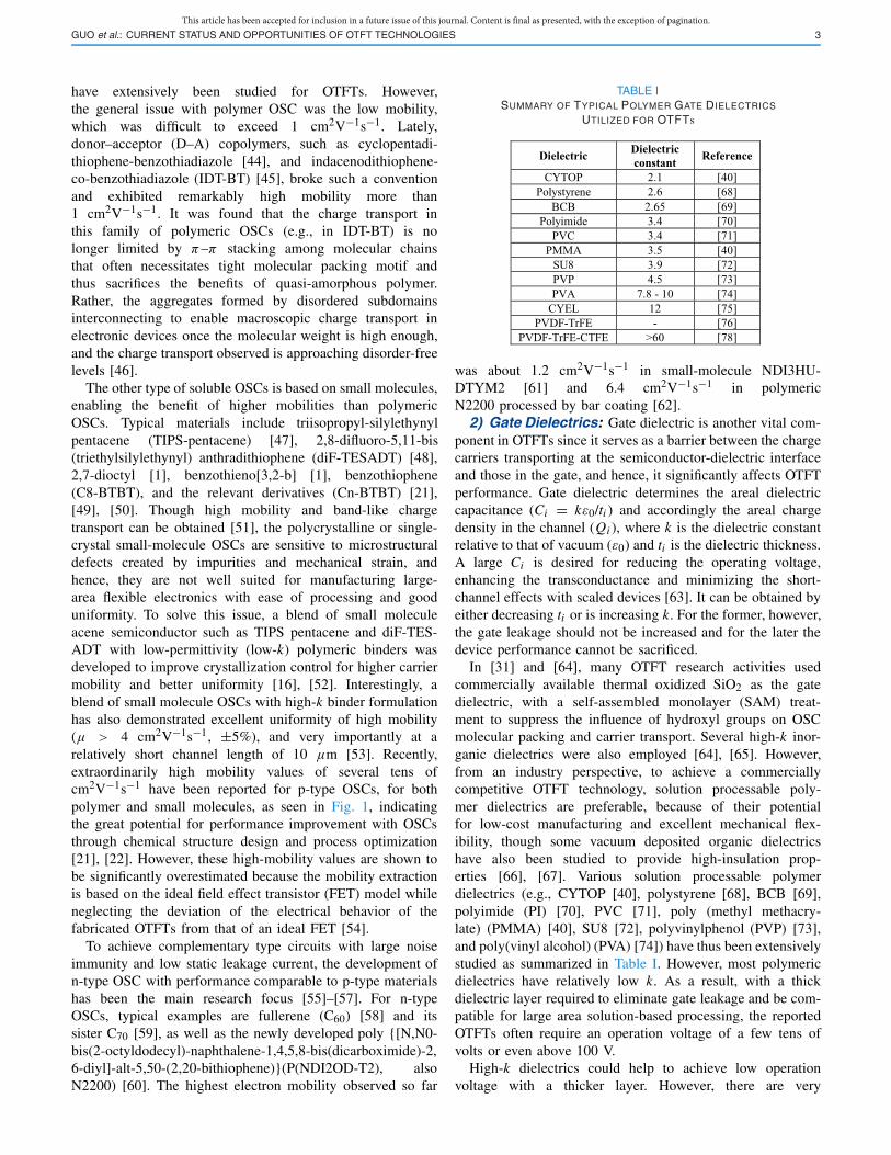
TABLE ISUMMARY OF TYPICAL POLYMER GATE DIELECTRICS
UTILIZED FOR OTFTs
was about 1.2 cm2V−1s−1 in small-molecule NDI3HU-DTYM2 [61] and 6.4 cm2V−1s−1 in polymericN2200 processed by bar coating [62].
2) Gate Dielectrics: Gate dielectric is another vital com-ponent in OTFTs since it serves as a barrier between the chargecarriers transporting at the semiconductor-dielectric interfaceand those in the gate, and hence, it significantly affects OTFTperformance. Gate dielectric determines the areal dielectriccapacitance (Ci = kε0/ti ) and accordingly the areal chargedensity in the channel (Qi ), where k is the dielectric constantrelative to that of vacuum (ε0) and ti is the dielectric thickness.A large Ci is desired for reducing the operating voltage,enhancing the transconductance and minimizing the short-channel effects with scaled devices [63]. It can be obtained byeither decreasing ti or is increasing k. For the former, however,the gate leakage should not be increased and for the later thedevice performance cannot be sacrificed.
In [31] and [64], many OTFT research activities usedcommercially available thermal oxidized SiO2 as the gatedielectric, with a self-assembled monolayer (SAM) treat-ment to suppress the influence of hydroxyl groups on OSCmolecular packing and carrier transport. Several high-k inor-ganic dielectrics were also employed [64], [65]. However,from an industry perspective, to achieve a commerciallycompetitive OTFT technology, solution processable poly-mer dielectrics are preferable, because of their potentialfor low-cost manufacturing and excellent mechanical flex-ibility, though some vacuum deposited organic dielectricshave also been studied to provide high-insulation prop-erties [66], [67]. Various solution processable polymerdielectrics (e.g., CYTOP [40], polystyrene [68], BCB [69],polyimide (PI) [70], PVC [71], poly (methyl methacry-late) (PMMA) [40], SU8 [72], polyvinylphenol (PVP) [73],and poly(vinyl alcohol) (PVA) [74]) have thus been extensivelystudied as summarized in Table I. However, most polymericdielectrics have relatively low k. As a result, with a thickdielectric layer required to eliminate gate leakage and be com-patible for large area solution-based processing, the reportedOTFTs often require an operation voltage of a few tens ofvolts or even above 100 V.
High-k dielectrics could help to achieve low operationvoltage with a thicker layer. However, there are very

This article has been accepted for inclusion in a future issue of this journal. Content is final as presented, with the exception of pagination.4 IEEE TRANSACTIONS ON ELECTRON DEVICES
few choices of suitable polymer dielectrics with highenough k values. Cyanoethylpullulan (CYEPL) [75], fer-roelectric polymer poly (vinylidenefluoride-trifluoroethylene)[P(VDF-TrFE)] [76], and relaxor ferroelectric polymerpoly(vinylidene fluoridetrifluoroethylene-chlorofloroethylene)[P(VDF-TrFE-CFE)] [77], [78] have been studied for low-voltage OTFTs. P(VDF-TrFE-CFE) was reported to have ak value above 60 [78]. When the high-k gate dielectric layeris directly interfacing the OSC channel, the energetic disordercaused by the dipoles in high-k dielectric would tend totrap carriers from gate bias induced conduction channel. Theresulted localization of charge carriers could cause not onlymobility degradation [40], but also increased hysteresis anddevice instabilities [79]. It was shown that, by inserting athin, low-k dielectric layer between the high-k one and theOSC channel, the dipole field can be effectively screened forimproved device performance [79]. In [80], it was found that,during spin coating of a blend of high molecule-weight PMMAwith P(VDF-TrFE), the high molecule-weight PMMA tendedto aggregate at the bottom of the deposited film, thus formingthe low-k/high-k bi-layer gate dielectric structure for OTFTsin a simpler way.
A type of solid polymer electrolytes, so-called ion gels,has also been studied as a gate dielectric for low-voltageOTFTs [81], [82]. The ion gel was obtained by blending ionicliquids with a gelating triblock copolymer to form a physicallycross-linked network and features very large specific capaci-tance exceeding 1 μF/cm2 with thickness of about 1 μm, sothat it can help to substantially reduce the operation voltageand simultaneously achieve very high driving currents. Despitethat, the long polarization time of the ion gel dielectric mayslow down the device operating speed, and the presence ofions in the solid electrolyte can cause electrochemical dopingof the channel, thus inducing reliability issues.
Furthermore, in the fabrication of OTFTs devices, the depo-sition of two or more layers sequentially by solution processescould cause dissolution or swelling of the underlayer. Cross-linking of the polymer dielectrics by photograph- or thermalreactions has been studied to enhance solvent resistance, andalso improve the electrical robustness [83]–[87].
3) Other Materials: With significant advances in funda-mental material development, the industry can now supplyvolumes of OSC and gate dielectric materials for substantialpilot scale manufacturing processes of low-temperature flex-ible display backplanes with the device performance greaterthan a-Si TFTs. These materials have either been commerciallyavailable materials, which have been evaluated for compati-bility or, in some cases, new materials have been synthesizedwith tailored properties. In addition to OSC and gate dielectricmaterials, other materials for substrate buffer layers, electrodetreatment and passivation layers are also of importance. In themultilayer integration structure, materials at different layershave to be well matched with solubility difference or be cross-linkable. The OSC/dielectric interface is a critical one forefficient charge transport, as is the back-channel of the OSClayer. Therefore, in a top gate device, it is necessary to controlthe buffer layer [88], while in a bottom gate device, selecting asuitable passivation layer is critical [89]. Additionally, metallic
Fig. 2. Illustration of the four device structures used for OTFTs.
source/drain (S/D) electrodes often require SAM treatmentto improve charge injection into the OSC layer [31]. TheS/D electrodes used in manufacturing as opposed to researchhave to be compatible with the industry available processesand at an acceptable cost. Alternatives to gold (Au) arevital to the success of the industry, with silver (Ag) [74],indium tin oxide (ITO) [90], molybdenum (Mo) [91], andcopper (Cu) [92] being amongst the list of some that havebeen investigated for this purpose. Therefore, the industryneeds to work on developing a full package of materialsalongside the OSCs to provide a total material solution forOTFT manufacturing.
B. Device Structure
As shown in Fig. 2, OTFTs can be implemented in fourdifferent structures depending on the relative locations of theelectrodes. For most of basic research, the inverted staggeredstructure is used with highly doped silicon as the gate andthermally oxidized silicon oxide as the gate dielectric based oncommercial silicon wafers for process simplicity [31]. Manyreported high-mobility OTFTs were also fabricated in thisway [15], [21], [22]. The coplanar structure was also recentlyrealized to obtain excellent field effect transistor characteristicsfor ambipolar polymer OSCs by selective contact doping usingp-type dopants [93]. However, these top-contact structures aredifficult for OTFT circuit integration over large area becauseof the process difficulty of making S/D metal electrodes on topof the OSC layer with precise patterning. For bottom contactstructures (inverted coplanar and staggered), the metal contactsare formed before deposition of the OSC layer, and can thusbe finely patterned by industry compatible photolithographyprocesses. Surface modifications of metal contacts with thiolSAMs can be used for obtaining low resistive and preferablyohmic metal/semiconductor contacts as well as good-qualitysemiconductor films on top of the S/D electrodes for higherperformance and better uniformity of electrical characteris-tics [94]. With these considerations, they are also the choicesin OTFT manufacturing trials in industry [95], [96]. Comparedto the inverted coplanar structure, the staggered structure has alower contact resistance for a larger effective area for carriers’injection at the source electrode. The contact resistance in thestaggered structure OTFT was also found to be less dependenton the contact barrier than that in the inverted coplanar one,attributed to gate field enhanced charge injection [97].
This article has been accepted for inclusion in a future issue of this journal. Content is final as presented, with the exception of pagination.GUO et al.: CURRENT STATUS AND OPPORTUNITIES OF OTFT TECHNOLOGIES 5
Contact effects are usually present in OTFTs and theymanifest by a reduction of effective mobility and transcon-ductance. For this reason, scaling of channel lengths may beproblematic, as the limiting effect of the contact becomesmore pronounced. However, deliberately introducing a contactenergy barrier may have beneficial effects despite the decreasein current and speed. A new structure named source-gatedtransistor (SGT) [98] is formed when a barrier (e.g., Schottky)at the source is used to restrict the current. Under normaloperation, at low drain bias, the source barrier is reversebiased and the semiconductor is depleted of carriers acrossits whole thickness, leading to saturation of output current atcomparatively low drain voltage. This allows energy-efficientoperation while maintaining high intrinsic gain, from lowerdrain voltages than conventional FETs, and current is mod-ulated in the first order by the gate electric field’s effect onthe effective source barrier height [99]. When this structure isapplied for OSCs, the induced high drain electrical field in thedevice may result in enhanced carrier mobility and operatingspeed [100]. As a result of the current control method, draincurrent is virtually independent of source–drain separation,which increases performance uniformity in high-throughputtechnologies with low-resolution patterning. Importantly, theSGT structure was normally realized in inverted staggeredstructure, and would also possible to be made in staggeredstructure. Therefore, SGT and the conventional FET can bemade on the same substrate, by varying the contact propertiesthrough choice of a different electrode metal or contact treat-ment, enabling the exploitation of both types of devices in thesame circuits.
C. Process and IntegrationThe most ideal approach for OTFT integration is full
additive printing for “manufacturing-on-demand” at a fractionof the cost and footprint. However, due to difficulties intechnology scaling for fine structures and complicated mul-tilayer integration, it is unrealistic today to use all additiveprinting processes for high-end applications, such as displaysand imagers, which have strict requirements on performance,integration density and reliability. In LCDs, e-paper displaysand X-imagers, OTFTs simply function as switches, while inOLED displays, OTFTs need to work as switches and currentdrivers and the pixel structure is much more complicated.Thus, it is clear in the short term, OTFT-based flexibleelectronics must be manufactured using more conventionalprocesses—by repurposing existing manufacturing equipmentto minimize barriers to entry and get products to marketthat validate the ‘product performance’ and applications andprove business cases for the value that OTFT can bring toapplications. In the meantime, lots of research is undergoingon addressing issues on all printing processes, for manyvery cost sensitive applications with less requirements on theintegration density and reliability.
1) Processes Compatible With Established IndustryFacilities: The display industry currently manufactures over150 million square meters of display backplanes per year onglass, which is supported by mature industry players rangingfrom materials suppliers to equipment vendors. In the near
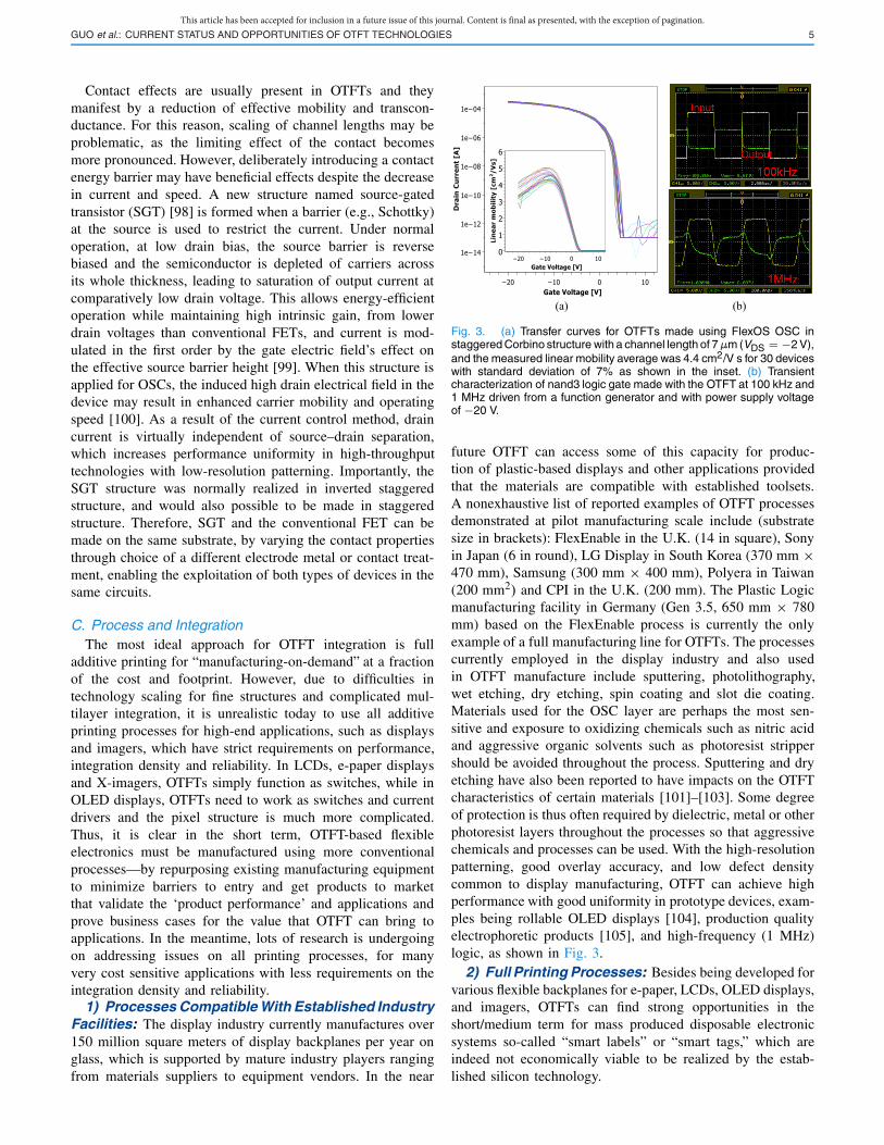
Fig. 3. (a) Transfer curves for OTFTs made using FlexOS OSC instaggered Corbino structure with a channel length of 7µm (VDS = −2 V),and the measured linear mobility average was 4.4 cm2/V s for 30 deviceswith standard deviation of 7% as shown in the inset. (b) Transientcharacterization of nand3 logic gate made with the OTFT at 100 kHz and1 MHz driven from a function generator and with power supply voltageof −20 V.
future OTFT can access some of this capacity for produc-tion of plastic-based displays and other applications providedthat the materials are compatible with established toolsets.A nonexhaustive list of reported examples of OTFT processesdemonstrated at pilot manufacturing scale include (substratesize in brackets): FlexEnable in the U.K. (14 in square), Sonyin Japan (6 in round), LG Display in South Korea (370 mm ×470 mm), Samsung (300 mm × 400 mm), Polyera in Taiwan(200 mm2) and CPI in the U.K. (200 mm). The Plastic Logicmanufacturing facility in Germany (Gen 3.5, 650 mm × 780mm) based on the FlexEnable process is currently the onlyexample of a full manufacturing line for OTFTs. The processescurrently employed in the display industry and also usedin OTFT manufacture include sputtering, photolithography,wet etching, dry etching, spin coating and slot die coating.Materials used for the OSC layer are perhaps the most sen-sitive and exposure to oxidizing chemicals such as nitric acidand aggressive organic solvents such as photoresist strippershould be avoided throughout the process. Sputtering and dryetching have also been reported to have impacts on the OTFTcharacteristics of certain materials [101]–[103]. Some degreeof protection is thus often required by dielectric, metal or otherphotoresist layers throughout the processes so that aggressivechemicals and processes can be used. With the high-resolutionpatterning, good overlay accuracy, and low defect densitycommon to display manufacturing, OTFT can achieve highperformance with good uniformity in prototype devices, exam-ples being rollable OLED displays [104], production qualityelectrophoretic products [105], and high-frequency (1 MHz)logic, as shown in Fig. 3.
2) Full Printing Processes: Besides being developed forvarious flexible backplanes for e-paper, LCDs, OLED displays,and imagers, OTFTs can find strong opportunities in theshort/medium term for mass produced disposable electronicsystems so-called “smart labels” or “smart tags,” which areindeed not economically viable to be realized by the estab-lished silicon technology.

This article has been accepted for inclusion in a future issue of this journal. Content is final as presented, with the exception of pagination.6 IEEE TRANSACTIONS ON ELECTRON DEVICES
Fig. 4. (a) Printed time-temperature dose tag showing the different sub-circuits and a photograph of the tag. Reprint with permission from [107].(b) For this tag, the transfer characteristics for 30 typical OTFTs usingp-type semiconductor or n-type semiconductor. The photographs showthe semiconductors printed over interdigitated electrodes.
The simplest applications are based on the all organic stand-alone system. For example, a low scale of integration logicblock was connected to a suitable sensor, i.e., a toggle buttonand/or a simple fuse, to detect the opening of a package,and can drive a simple display showing the status of suchpackage [106]. Such simple, stand-alone, yet effective tag,could be attached to the package in the same way a normalgraphical label is, sharing a very similar geometrical formfactor and mechanical properties, provided that a suitableinterconnection to the sensor is guaranteed. Such possibilitymust, however, be sustained by the development of high-throughput, yet reliable printing processes, capable of keepingthe overall tag cost extremely low. As shown in Fig. 4(a),a time-temperature dose tag was fabricated on flexible plas-tic foil and comprised a thermistor divider, complementaryorganic circuits, and two nonvolatile memory cells [107], afterachieving having reasonable device uniformity of both p- andn-type OTFTs with additive printing processes [Fig. 4(b)].If integrated with an appropriate power supply, the tag couldoperate as a stand-alone system, with nonvolatile memory forlater readout for a wide range of potential applications infood and medicine spoilage. It is a promising step towardeconomical printed OTFT stand-alone sensor systems.
For the commercially available batteries used as the powersupply for these stand-alone systems, the output voltage levelof around 1.5–4 V is often insufficient to surpass the thresholdvoltage for many printed OTFTs that have been demonstratedso far. In order to operate the system, either the supply voltagemust be increased or the operation voltage of OTFTs should
be reduced. The supply voltage can be boosted by connectingbatteries in series or by adding a voltage multiplier [108]or charge pump circuit [109], which, however, increasesthe system complexity and cost. Low-voltage operable andstable OTFT is thus very important for this system, but itis challenging to be achieved by only enlarging the gatedielectric capacitance with ultrathin or high-k gate dielectriclayer, especially when the devices need to be manufacturedby all additive printing processes to make a commerciallyviable technology. Recently, several studies have shown thatit is feasible to reduce the subgap density of states (DOS)at the channel through solution processed OSCs for real-izing low-voltage OTFTs with small gate dielectric capaci-tance [74], [110]. Therefore, a relatively thick low-k polymerdielectric can be applied, which can help to achieve excellentstability and also has wide material choices [71], [72], [83],[86], [87]. Such a low-voltage OTFT can be fabricated byinkjet printing all layers including electrodes, gate dielectric,OSC, and encapsulation layers, proving the most economicmanufacturing approach [111].
For more envisioned applications, which need to havewireless connections with users, the stand-alone system is notapplicable. In such systems, a series of functions, includingaccurate and complex signal processing, power managementand communication are required to be performed in a severelypower constrained system. These functions are very chal-lenging to be realized with printed OTFTs today. A hybridtechnology is thus necessary to combine the OTFT with low-voltage silicon chips [112]. In such a system as illustratedin Fig. 5, a transducer circuit is implemented using printedOTFTs to convert the sensed signal to a standard voltage out-put. Various functional sensing materials can also be integratedthrough the printed OTFT technology. A common read-out andsignal processing hardware or specific silicon chip consistingof analog-to-digital converter, processor, wireless interface fordata output (e.g., near-field communication, Bluetooth, …)can thus be implemented for these different sensors. With afixed silicon chip design and additive printing of the OTFT-based front end for the custom design, this hybrid integrationwould provide a low cost and versatile solution to “smarttag” systems. For this integration, with the fully-printablelow voltage and stable OTFT, sensor tags were made to beoperated in a low-voltage (3.3 V) battery powered electronicsystem for long term and repeatable ammonia and pH sensing,respectively [24], [71].
Compared to the hybrid solution with a silicon chip, a “chip-less” design would be desired to provide a lower cost solutionfor wireless sensor tags by seamlessly integrating all therequired electronics, sensing and antenna driving functionali-ties [113], [114]. For that, high speed printed OTFTs to affordsignal modulation frequency of at least tens of megahertz areneeded to construct the wireless communication interfaces.The transition frequency or cutoff frequency fT is widelyadopted for the evaluation of the operation speed of a singletransistor [115]–[118]. Two methods were generally adoptedfor measuring fT : a direct evaluation of the transconductanceand gate capacitance via the measurement of small currentsignals flowing into the device electrodes [116], [117] or

This article has been accepted for inclusion in a future issue of this journal. Content is final as presented, with the exception of pagination.GUO et al.: CURRENT STATUS AND OPPORTUNITIES OF OTFT TECHNOLOGIES 7
Fig. 5. Illustration of a hybrid integration approach combining theadvantages of both the printed OTFT and the silicon technology.
Fig. 6. Overall comparative plot of the best fT results for OTFTs, whichfT was explicitly measured and reported in the literature. The worksare classified with respect to the fabrication methods adopted for thepatterning of the electrodes and for the deposition of the semiconductor.
the evaluation of the two-port-network h21 hybrid parame-ter [118]. Enhancing fT of OTFTs requires the adoption ofOSC materials guaranteeing high effective mobility and archi-tectures with scaled channel lengths and reduction of parasiticcapacitances posing constraints on the patterning technologythat has to be maintained compatible with cost-effective large-area processes. Fig. 6 summarizes the measured fT of OTFTsfrom selected works achieving the best results, which areclassified with respect to the fabrication methods adopted forthe patterning of the electrodes and for the deposition of theOSC layer [43], [118]–[127]. The record fT reported to datereaches the value of 27.7 MHz for a device based on C60 witha channel length of 2 μm defined by photolithography [119].Recently, OTFTs with fT of 20 MHz were fabricated by meansonly of scalable coating techniques and laser-based direct-writing methods with a completely mask-less procedure [124].A much higher throughput approach was demonstrated byKang et al. [126], who used highly scaled gravure printing tofabricate OTFTs with a fast printing speed of 1 m/s, despitea lower fT = 0.3 MHz. It is important to highlight thatthose high fT values were generally achieved with operationvoltages of several tens of volts. Indeed, to comply with therequirement of low-voltage operation which is necessary forapplications in the fields of wearable and portable devices,it is desirable to achieve high-frequency operation for asupply voltage lower than such a value. The works where
Fig. 7. Comparison of the number of parameters in the developedUOTFT model in commercial circuit simulator SmartSPICE with themodels for silicon FETs.
high-frequency operation is combined with low-voltageoperation are a minority. The representative work byZaki et al. [118] obtained ft = 3.7 MHz for a bias voltage aslow as 3 V.
D. Device Modeling and Circuit Design
Accurate compact models are basis for efficient circuitdesign to move the OTFT technology from devices to cir-cuits and systems. In the past, corresponding developmentof physics-based compact models has been under continuousprogress, after many fundamental aspects of OTFTs wererevealed [128], [129]. Models to be able to capture non-ideal realistic device behaviors, including gate bias (VGS)dependent mobility [130], [131], nonexponential dependenceof subthreshold current on VGS [132], [133], and contactresistance effects [134], have been developed. Smooth linear-to-saturation transition and subthreshold to above-thresholdtransition were further worked out to connect these discretemodels for unified compact models, which cover all regimesof OTFT operations and are able to be implemented into circuitsimulators to reach an effective convergence [130], [135].For the large variations in OTFT materials and structures,further modeling efforts have been devoted to the capabilityof rearrangement and flexibility for capturing the essence inthe behaviors of various OTFTs in a consistent and relativelysimple way, and allowing for easier implementation, modifica-tions, and parameter extraction [128], [136]. These developedmodels can be conveniently implemented into commercialcircuit simulator for circuit simulation using Verilog-A, which,however, is slower and less efficient than a well-developedSPICE model [137]. Currently, the only OTFT SPICE modelavailable in commercial circuit simulator is the universalOTFT (UOTFT) model in SmartSPICE, which combines therobust concepts of universal charge-based FET modeling withOTFT specific charge, mobility and contact resistance bias,and temperature dependence [138]. The parameters in theUOTFT are significantly less than that in those advancedmodels for modern silicon FETs, as shown in Fig. 7.
To design and construct complex circuits and systems, thecomplementary type is a preferred choice for its low staticpower, rail-to-rail operation, and large noise margin [139].

This article has been accepted for inclusion in a future issue of this journal. Content is final as presented, with the exception of pagination.8 IEEE TRANSACTIONS ON ELECTRON DEVICES
Fig. 8. Comparisons of different unipolar circuit styles for OTFTs.
However, it is difficult to find n- and p-type semicon-ductor materials with equivalent performance and com-patible processes that would allow easy fabrication ofhigh-performance complementary circuits. For print process-ing, complementary design is easy to realize since the twosemiconductors are additively patterned in just two steps.For photolithographic processing, at least three more maskingsteps are required to pattern two semiconductors due to thesubtractive process. Therefore, the unipolar designs have beenwidely adopted for OTFT logic circuits. Although havingthe advantage of simplicity, the common unipolar logic cir-cuit design could hardly provide sufficient noise margins toaccommodate normal OTFT parameter variations for buildingcomplex circuits. To improve the robustness to parametricvariability, advanced device or circuit architectures such aspseudo CMOS [140], dual-Vth TFT logic [141], and dual-gate structure [142] were proposed. Therefore, considering thetradeoff among performance, process simplicity and designcomplexity as shown in Fig. 8, it would be helpful to predictthe yield and the performance in the early device develop-ment or circuit design stage to select the most cost-effectivesolution for realizing the required functional circuit of goodmanufacturability [143], [144].
E. EDA Tools and Design KitsElectronic design automation (EDA) tools have been a key
factor for the success of the microelectronic industry since theyallowed building complex (nonregular) integrated circuits withan increasing number of transistors (according the Moore’sLaw) in a reduce amount of time. EDA tools strongly devel-oped the concept of technology-independent circuit design thatis later mapped into technology dependent cells and structures(based on transistor models and design rules), that weredescribed in the technology or process design kit [technologydesign kit or process design kit (PDK)] available for everystable technological process. This leads to the concept of fab-only and fabless semiconductor industry. Fab-only consistsof companies that does not produce semiconductor productsor chips being commercialized (i.e., TSMC or UMC) whilefab-less companies are concentrated in application-orientedtechnology-independent that do not own fabrication processes(i.e., Qualcomm or ARM both around the mobile industry).
Fig. 9. (a) View of the current silicon microelectronics industry wheremany fabless industries develop a wide range of products implementedin a reduced set of fab facilities thanks to its highly segmented horizontalbusiness model. (b) View of the current flexible electronics industry with areduced set of products that have a wide range of technologies availablefor its implementation in a closed vertical business model.
As shown in previous sections, design of future flexiblesystems based on OTFTs will include heterogeneous integra-tion of different technologies (flexible + silicon, flexible +flexible, flexible + functionalization). Moreover, there is alsoan increase of homogeneous integration systems (displays +logic + actuators, sensors + processing + antenna) in a giventechnology and substrate. Both approaches require the imple-mentation of complex integrated functionalities that requiredmixing different design disciplines and methods. Currently,there is not any single EDA tool capable of coping allthose aspects that require not only the corresponding devicemodeling but also mixed-mode simulators, variability analysisand detailed layout extraction tools.
Big players in the EDA industry such as Synopsys, Cadence,or Mentor Graphics can cover almost all design aspects.Their tools allow very high design productivity at the costof expensive licenses. Part of this design productivity comesfrom the fact that any given circuit or structure can be easilyand quickly redesigned for a different technology or processvariation thus strongly reducing circuit any redesign effort.Technology dependent tools are ready to use and the methodsto add the information related to any OTFT or general TFTtechnologies are specified around the PDK concept [145].However, those big players are not yet paying attention tospecific tools for OTFT- or TFT-based systems. The mainreason is that the process technology has a very wide rangeof choices, while existing valued market applications is muchless compared to that of the silicon microelectronics industryas illustrated in Fig. 9.
Other EDA tools used for OTFT circuit design are asfollows.
1) Other low-cost PC-based EDA tools (i.e., Tanner orPhoenixBV).
2) Tools coming from the display industry (i.e., Silvaco)that include a strong link with device level simulation.
3) The large set of tools coming from the printed circuitboard industry that is weekly connected with simulationbut allow checking geometrical and electrical designrules before sending the circuit for fabrication, and aremuch cheaper.

This article has been accepted for inclusion in a future issue of this journal. Content is final as presented, with the exception of pagination.GUO et al.: CURRENT STATUS AND OPPORTUNITIES OF OTFT TECHNOLOGIES 9
Fig. 10. (a) Performance roadmap in terms of mobility for the OTFTtechnology in FlexEnable. (b) Measured transfer performance of thecurrent OTFT fabricated in FlexEnable with a channel length of 5 µmand a channel width of 50000 µm.
4) Open-source or free tools (i.e., Glade, Klayout,Alliance).
5) There are still a high number of designs that are justbeing designed with graphic editors.
EDA tools are usually related with design methodolo-gies that have been traditionally classified as device-based(or full-custom) and cell-based (or semicustom). CurrentOTFT circuits require low design effort compared with siliconones [146]. Most of the implemented designs are still devicebased [23], [147], [148] so that designers and up by drawingthe final circuit layouts. Nonetheless, there are several circuitsthat are already been built using cell-based design techniquesthat include some degree of automation in the placement androuting, such as standard-cells or gate-arrays [149]–[151].
A novel circuit design initiative is devoted to let designersuse the capabilities of digital printing on top of TFTs builtwith other technologies for building circuits to improve theirfunctional or performance characteristics by adding identifica-tion codes, calibration circuits, programmable memory or adhoc arithmetic circuits. Examples are: 1) user-customizablelogic paper with sea-of-transmission-gates of organic CMOSand inkjet printed interconnects [151]; 2) programmable logiccircuits (PAL) for functional integrated smart plastic sys-tems [106]; 3) print-programmable read-only memory [152];and 4) inkjet-configurable gate arrays with high-resolutionOTFTs and inkjet printed interconnecting dots [153].
F. Applications and Status of Industrialization
The OTFT backplane technology developed by FlexEn-able (previously Plastic Logic) is the first and possibly onlyOTFT technology used in products today. The products aree-paper displays manufactured by Plastic Logic Germany(e.g., popSLATE, an iPhone cover containing a OTFT-drivenflexible e-paper display). Within the past two years, the OTFTperformance has risen to be above that of a-Si TFT forall key electrical parameters including mobility, stability anduniformity, opening up possibilities for a wide range of newapplications. As shown in Fig. 10(a), the mobility of the OTFTis now about 1.5 cm2V−1s−1 at a channel length less than5 μm. A separate but often less-discussed electrical benefitof OTFT is leakage current. Compared with a-Si TFTs, theOTFT can easily have leakage currents two or even threeorders lower. Fig. 10(b) is the measured transfer curve of
Fig. 11. Illustration of the integration structure and the photographs ofthe developed flexible system applications based on the OTFT backplanetechnology from FlexEnable.
an OTFT with a channel width of 50 000 μm in order tomeasure the leakage. It can be seen that even with such alarge channel width, leakage is still lower than the noise inthe test system—indicating very low true leakage current lessthan 10−17 A/μm for the device. This very low leakage bringsbenefits to displays in allowing low-frame rate driving (powersaving), and also to sensors, enabling greater sensitivity, whichfor applications like X-ray sensors means the use of lowerdoses. Besides the e-paper displays, a series of more advanceddisplay and sensor applications have been demonstrated withthis OTFT technology, as shown in Fig. 11.
In addition to array backplanes, simple OTFT circuitry ispromising for bio-sensor applications. Most of the OTFT-based biosensors, including organic FETs and organic elec-trochemical transistors, are potentiometric transducers [19].A little change in the effective gate voltage will lead to apronounced channel current response. Therefore, due to theirinherent amplification functions, good biocompatibility, highmechanical flexibility, and ease of miniaturization/integration,OTFTs have emerged as a versatile platform for biologicalapplications. Recently, different types of biosensors, includingenzyme [154], deoxyribonucleic acid [155], cells [156], neuron[157], and bacteria and protein sensors [158], [159], havebeen successfully developed based on the interactions betweenbiological analytes and organic channel or gate electrode ofan OTFT modified with specific biomolecules and functionalmaterials. Although OTFT-based biosensors have not yet beencommercialized, some devices including enzyme sensors mayfind big market in the future. For examples, glucose sensoris a very important healthcare product since the population ofdiabetes mellitus in the world increases every year. The preva-lence of diabetes for all age groups worldwide was estimatedto be 2.8% in 2000 and 4.4% in 2030 [160]. Currently, theoperation of all of the blood glucose meters in the marketis based on finger stick assays, which is painful and cancause stress to the patient. Therefore, developing noninvasiveglucose meter with high accuracy becomes the trend of bloodglucose determination. OTFT-based enzyme biosensors canbe used for noninvasive glucose detection by measuring theglucose level in body fluid, which may have a huge marketin the future [161]. Other enzyme biosensors, like uric acidand cholesterol sensors, are also very useful in healthcareproducts. Nevertheless, the commercialization of OTFT-based

This article has been accepted for inclusion in a future issue of this journal. Content is final as presented, with the exception of pagination.10 IEEE TRANSACTIONS ON ELECTRON DEVICES
biosensors relies on the development of fabrication techniquesfor mass production and the synthesis of biocompatible andstable OSCs specifically for biological applications.
III. CHALLENGES AND OUTLOOK
The above review shows massive progresses on all aspectsof the OTFT technologies. However, to become a widelyadopted technology for the envisioned applications, there arestill lots of challenges ahead to be addressed. This part willtry to clarify these key challenges.
First, in terms of materials, there is still lack of materialstacks to be used for producing high performance, stableand uniform OTFTs in large area compatible processes. Thecurrent OTFT community is perhaps too focused on chargemobility of materials as a figure of merit. The processes anddevice structures used for testing the material performance arenot for scalable manufacturing. A greater emphasis shouldbe placed on other attributes such as uniformity, stability,manufacturability and short channel device performance. Inaddition, as highlighted by a recent paper, mobility estimationfrom nonideal FET current–voltage characteristics typical forOTFTs has been shown to produce values that are incorrectby an order of magnitude or more [54]. When the highperformance does not translate into the expected performancein the types of devices used in manufacturing, then thisreduces confidence of the technology as a whole. Possiblythe figures of merit for materials and devices should bedefined by the electronic design community since they arethe ones who will produce designs in the technology thatmeets the specifications of end users. Moreover, many physicaland chemical interactions between the OSC layer and otherdielectric, metal and interfacial layer materials in the devicestack are not only important for initial device performance butare critical for control of the device stability under electricalstress [162]. In addition to performance, material stacks alsoneed to be developed for processing OTFTs to be able to meetthe strict reliability test requirements, which are defined byapplications. Deep understanding of the instability issues ofOTFTs and finding the solutions to develop stable and reliableOTFTs is thus of great importance [163].
The challenge with device uniformity has been the othermain hurdle to practical large-scale OTFT circuits [25], [28],[107], [164]–[166]. In the comparison between all printedOTFTs [107] and the vacuum processed ones of finely pat-terned electrodes [25], similar level of performance variationscan be observed, indicating that the main source of variationsin OTFT devices mainly comes from the OSC film. The largedevice performance variations lead to decreased circuit noisemargin and thus poor yield. Therefore, to improve circuityield, the device uniformity need to be improved by eithermolecule level design to reduce material disorder [46], [167]or developing processing techniques for better crystallizationcontrol of the OSC film [168].
Second, there is no standard material stacks, device /inte-gration architectures, and manufacturing processes for thewhole community to work with. Diversity of materials choices,device structures, and processes are advantages of OTFTsto provide a versatile technology platform. However, it also
brings challenges to the whole community to work togetherto address the common technology issues and build anindustry chain toward commercialization like that in siliconsemiconductor industry. For different types of applications,the processing approaches would vary to have the optimalbalance between the performance and the cost. For example,for high-resolution flexible display or imagers application,standard manufacturing and device integration architecturecan be constructed based on the well-established processesin the display industry, including sputtering, photolithography,wet/dry etching, spin coating and slot-die coating. The largematerial research community can thus have clear objectives ofmatching the device integration and manufacturing processes,while achieving required performance. While the ongoingmaterial and process research is valuable in tackling currentand future device performance obstacles, the development ofrobust design tools require stable materials and processes.The development of industry standard OTFT compact models,and associated process/technology design tools is essentialto lower the entry barrier for product designers. The designcommunity will continuously add functionality and IP valuewhich in turn leads to greater technology dissemination andadoption. Owning a strong design community will be ableto speed up product development cycles, maximize the per-formance capability of the technology, and exploit the newapplications based on the technology. Prerequisite to this isthe development of manufacturing design rule manuals andstandardized process design kits. Inbuilt in this are manychallenges related to compact model parameter extractiontemplates, meaningful layout, design rule check tools and aseamless design automation flow.
An important advantage of OTFTs is that they can be man-ufactured by printing, eventually allowing a highly customizedfabrication of organic and hybrid integrated circuits, especiallywhen digital printing techniques are adopted, ultimately hand-ing an on-demand electronics. This concept which has beendeveloped at research level in the last one or two decades needsto face a reality where such tools that would allow this shiftof paradigm in electronics fabrication, are not yet developedoutside the laboratories. Therefore, printing OTFTs allowingdesign and custom fabrication of circuits needs more workon standardization of materials, components and processes,design tools and accessible fabrication tools.
The separation between fabs and fabless industries is pop-ular for other mass market domains apart from the semi-conductor industry (i.e., the traditional printing industry) butit is not for niche oriented domains (i.e., displays or microelectromechanical system). The integration of circuit withOTFTs seems to show that there will be room for massproduction for a wide range of applications, as illustrated inFig. 12. If this happens, fabs will open their technologies to theapplication-oriented industries by providing PDKs (geometricand simulation information) and clear cost models. Openingaccess to technologies will for sure boost and enlarge theapplications since it will lower the entry barriers for thoseindustries. Different initiatives have already set the basis forbuilding this path [169], [170] and have demonstrated thefeasibility of using this model to build complex systems.

This article has been accepted for inclusion in a future issue of this journal. Content is final as presented, with the exception of pagination.GUO et al.: CURRENT STATUS AND OPPORTUNITIES OF OTFT TECHNOLOGIES 11
Fig. 12. Future view of the OTFT-based large area electronics industrywith a wide set of products for different applications that profit from a widerange of hybrid technologies available for its implementation in an openhorizontal business model through the integration of their PDKs into theEDA tools.
Third, tradeoffs between performance and large area lowcost processing need to be much better balanced. Strongopportunities can be opened for OTFTs with a suitable com-bination of mass-scale processes and suitable performances.Clearly, these two goals require tradeoffs, since large-areamanufacturing poses constraints for example on critical fea-tures, thus ultimately limiting performances. A clear chal-lenge, therefore, is to develop methodologies characterizedby a high patterning resolution, down to the micrometer size,while maintaining scalability, compatibility with cheap plasticfoils and a reasonable throughput. Aggressive downscaling offeatures size to a sub-micrometer level may not be required, asback on the envelop estimations return tens of megahertz oper-ation of OTFT with micrometer scale channels and mobilityin the 1–5 cm2V−1s−1 if capacitive parasitism is kept undercontrol. Overall, the challenge in this respect can be pinneddown to the control of the device footprint and capacitiveparasitism, possibly benefiting from approaches previouslyadopted in established technologies, such as self-alignment,while maintaining a suitably high yield.
Another tradeoff is between reducing the operation volt-age and having device structures compatible with large areasolution-based processing. Most of those envisioned appli-cations of OTFTs are portable or wearable, requiring thedevices to be integrated in severely power-constraint electronicsystems with battery or ac. field. This poses a stringent require-ment on the operation voltage of the OTFT circuitry, whichin principle should be scaled down to 3 V, or even below.However, for OTFTs over large area substrates, especiallybased on solution processed multilayer integration, the gateinsulator layer needs to be thick enough (at least a few hundrednanometers) for the concern of device reliability and yield.Therefore, lots of work on using high-k gate dielectric materialor even solid electrolytes to realize low voltage with a thickdielectric layer [81], [84]. The issue for high-k gate dielectriclayer is that high-k dielectric materials could be unfavor-able for carrier transport due to the broadening of the trap
Fig. 13. Illustration of between and having device structures compat-ible with large area solution-based processing by using different gatedielectric technologies for reducing the operation voltage.
DOS at the semiconductor/dielectric interface by the formeddipole disorder [40]. The solid electrolyte can even induceelectrochemical doping of the channel due to the presenceof ions affect, causing reliability issues and slow operationspeed [85]. As summarized in Fig. 13, for the conventionalway of enlarging the gate dielectric capacitance to reduce theoperation voltage, there is tradeoff between processability andperformance requirements. A promising solution is to reducethe subgap DOS at the channel through solution processedOSCs, and thus, very small gate dielectric capacitance canbe used to realize low operation voltage [77], [112]. Thisapproach provides the possibility of using a wide range oflow-k polymer dielectric materials in a relatively thick layerto achieve stable low-voltage OTFTs [69], [74], [75], [88].
Last but not least, focused applications needs to be clearlydefined. The technology platform in FlexEnable (previouslyPlastic Logic) has demonstrated that there are no fundamentalproblems with the OTFT technology for commercialization.It is also shown that OTFT has huge market potential, andcan completely change our view of where and how electronicsis used in our daily lives. However, confidence in the OTFTtechnology might be increased if a greater number of fab orpilot lines existed with a predictable yield and uniformity.On the other hand, however, investments would not be put onconstructing new fab or pilot lines or even upgrading existingfabs for OTFT manufacturing if no clear applications wereseen.
Therefore, with a near-overwhelming list of applications(both existing and new markets), OTFT technology companiesneed, therefore, to focus on the right applications. Buildingpartnerships with other parts of the supply chain is critical tobuilding an ecosystem for the OTFT technology, and allowstechnology companies to focus on their respective areas ofexpertise.
IV. CONCLUSION
The review of research and development progresses in allaspects ranging from fundamental material and device researchto manufacturing trials in last decades shows that solid basishas been formed for the OTFT technology to become com-mercially successful. However, to eventually become a widely

This article has been accepted for inclusion in a future issue of this journal. Content is final as presented, with the exception of pagination.12 IEEE TRANSACTIONS ON ELECTRON DEVICES
adopted technology for the envisioned applications, there arestill lots of challenges ahead to be addressed. The first oneis to develop OTFT material stacks capable of producinghigh performance, stable, and uniform OTFTs in large areacompatible processes.
The second challenge would be how to define standardmaterial stacks, device/integration architectures, and manufac-turing processes to allow the whole community to work onthe common issues, and also reduce the entry barrier for thedesign community. How to balance the device performanceand the large low-cost manufacturability is also importantto meet the application requirement. Finally, with a near-overwhelming list of applications (both existing and newmarkets), focused applications need to be clarified, from whichdifferent requirement on the device performance, uniformity,and manufacturing scale of OTFTs can then be defined.To address these challenges, the whole community needs clearapplication and technology roadmaps and also standards interms of materials, device/integration structures, and processesto work together.
ACKNOWLEDGMENT
The authors would like to thank Dr. T.-Y. Chu fromNational Research Council, Canada, and Dr. J. Zhang fromthe Changzhou Institute of Printed Electronics Industry, China,for fruitful discussions at the panel discussion at the 2016Computer Aided Design for Thin-Film Transistor Technolo-gies held in Beijing during October 26–28, 2016.
REFERENCES
[1] A. Nathan, A. Ahnood, J. Lai, and X. Guo, Large Area Electronics,J. Burghartz, Ed. New York, NY, USA: Wiley, 2013.
[2] R. A. Street, “Thin-film transistors,” Adv. Mater., vol. 21, no. 20,pp. 2007–2022, May 2009.
[3] Y. Kuo, Thin Film Transistors: Amorphous Silicon Thin Film Transis-tor, vol. 1. The Netherlands: Springer, 2004.
[4] S. D. Brotherton, Introduction to Thin Film Transistors: Physics andTechnology of TFTs. Switzerland: Springer International Publishing,2013.
[5] K. Nomura, H. Ohta, A. Takagi, T. Kamiya, M. Hirano, and H. Hosono,“Room-temperature fabrication of transparent flexible thin-film tran-sistors using amorphous oxide semiconductors,” Nature, vol. 432,no. 4016, pp. 488–492, Nov. 2004.
[6] T. Kamiya and H. Hosono, “Material characteristics and applicationsof transparent amorphous oxide semiconductors,” NPG Asia Mater.,vol. 2, no. 1, pp. 15–22, Jan. 2010.
[7] A. Nathan et al., “Flexible electronics: The next ubiquitous platform,”Proc. IEEE, vol. 100, pp. 1486–1517, May 2012.
[8] L. Petti et al., “Metal oxide semiconductor thin-film transistors forflexible electronics,” Appl. Phys. Rev., vol. 3, no. 2, p. 021303, 2016.
[9] A. C. Arias, J. D. Mackenzie, I. McCulloch, J. Rivnay, and A. Salleo,“Materials and applications for large area electronics: Solution-basedapproaches,” Chem. Rev., vol. 110, no. 1, pp. 3–24, 2010.
[10] H. T. Yi, M. M. Payne, J. E. Anthony, and V. Podzorov, “Ultra-flexiblesolution-processed organic field-effect transistors,” Nature Commun.,vol. 3, p. 1259, Dec. 2012.
[11] K. Fukuda et al., “Fully-printed high-performance organic thin-filmtransistors and circuitry on one-micron-thick polymer films,” NatureCommun., vol. 5, p. 4147, Jan. 2014.
[12] J. Y. Oh et al., “Intrinsically stretchable and healable semiconduct-ing polymer for organic transistors,” Nature, vol. 539, pp. 411–415,Nov. 2016.
[13] Y. Lee, M. Shin, K. Thiyagarajan, and U. Jeong, “Approaches tostretchable polymer active channels for deformable transistors,” Macro-molecules, vol. 49, no. 2, pp. 433–444, 2015.
[14] N. A. Minder, S. Lu, S. Fratini, S. Ciuchi, A. Facchetti, andA. F. Morpurgo, “Tailoring the molecular structure to suppress extrin-sic disorder in organic transistors,” Adv. Mater., vol. 26, no. 8,pp. 1254–1260, Feb. 2014.
[15] Z. B. Henson, K. Müllen, and G. C. Bazan, “Design strategies fororganic semiconductors beyond the molecular formula,” Nature Chem.,vol. 4, pp. 699–704, Aug. 2012.
[16] J. Smith et al., “Solution-processed organic transistors based on semi-conducting blends,” J. Mater. Chem., vol. 20, no. 13, pp. 2562–2574,2010.
[17] T. Someya, A. Dodabalapur, J. Huang, K. C. See, and H. E. Katz,“Chemical and physical sensing by organic field-effect transistors andrelated devices,” Adv. Mater., vol. 22, no. 34, pp. 3799–3811, Sep. 2010.
[18] Y. Guo, G. Yu, and Y. Liu, “Functional organic field-effect transistors,”Adv. Mater., vol. 22, no. 40, pp. 4427–4447, Sep. 2010.
[19] P. Lin and F. Yan, “Organic thin-film transistors for chemical andbiological sensing,” Adv. Mater., vol. 24, no. 1, pp. 34–51, Jan. 2012.
[20] H. Sirringhaus, “Organic field-effect transistors: The path beyondamorphous silicon,” Adv. Mater., vol. 26, pp. 1319–1335, Mar. 2014.
[21] Y. Yuan et al., “Ultra-high mobility transparent organic thin film tran-sistors grown by an off-centre spin-coating method,” Nature Commun.,vol. 5, p. 3005, Jan. 2014.
[22] B. H. Lee, G. C. Bazan, and A. J. Heeger, “Doping-induced carrierdensity modulation in polymer field-effect transistors,” Adv. Mater.,vol. 28, no. 1, pp. 57–62, Jan. 2016.
[23] K. Myny, E. van Veenendaal, G. H. Gelinck, J. Genoe, W. Dehaene,and P. Heremans, “An 8-bit, 40-instructions-per-second organic micro-processor on plastic foil,” IEEE J. Solid-State Circuits, vol. 47, no. 1,pp. 284–291, Jan. 2012.
[24] W. Tang et al., “Low-voltage pH sensor tag based on all solutionprocessed organic field-effect transistor,” IEEE Electron Device Lett.,vol. 37, no. 8, pp. 1002–1005, Aug. 2016.
[25] W. Xiong, Y. Guo, U. Zschieschang, H. Klauk, and B. Murmann,“A 3-V, 6-bit C-2C digital-to-analog converter using complementaryorganic thin-film transistors on glass,” IEEE J. Solid-State Circuits,vol. 45, no. 7, pp. 1380–1388, Jul. 2010.
[26] M. Kaltenbrunner et al., “An ultra-lightweight design for imperceptibleplastic electronics,” Nature, vol. 499, no. 7459, pp. 458–463, Jul. 2013.
[27] B. C.-K. Tee et al., “A skin-inspired organic digital mechanoreceptor,”Science, vol. 350, no. 6258, pp. 313–316, 2015.
[28] R. A. Street et al., “From printed transistors to printed smart systems,”Proc. IEEE, vol. 103, no. 4, pp. 607–618, Apr. 2015.
[29] H. Klauk, “Organic thin-film transistors,” Chem. Soc. Rev., vol. 39,no. 7, pp. 2643–2666, Apr. 2010.
[30] J. Zaumseil and H. Sirringhaus, “Electron and ambipolar transport inorganic field-effect transistors,” Chem. Rev., vol. 107, pp. 1296–1323,Mar. 2007.
[31] Y. Wen, Y. Liu, Y. Guo, G. Yu, and W. Hu, “Experimental techniquesfor the fabrication and characterization of organic thin films for field-effect transistors,” Chem. Rev., vol. 111, no. 5, pp. 3358–3406, 2011.
[32] H. Lee, H. H. Choi, D. H. Kim, and K. Cho, “Microstructure dependentbias stability of organic transistors,” Adv. Mater., vol. 26, no. 11,pp. 1660–1680, Mar. 2014.
[33] C. Reese, M. Roberts, M.-M. Ling, and Z. Bao, “Organic thin filmtransistors,” Mater. Today, vol. 7, no. 9, pp. 20–27, Sep. 2004.
[34] G. Gelinck, P. Heremans, K. Nomoto, and T. D. Anthopoulos, “Organictransistors in optical displays and microelectronic applications,” Adv.Mater., vol. 22, no. 34, pp. 3778–3798, Sep. 2010.
[35] A. Facchetti, “Semiconductors for organic transistors,” Mater. Today,vol. 10, no. 3, pp. 28–37, Mar. 2007.
[36] K.-J. Baeg, M. Caironi, and Y.-Y. Noh, “Toward printed integratedcircuits based on unipolar or ambipolar polymer semiconductors,” Adv.Mater., vol. 25, no. 31, pp. 4210–4244, Jun. 2013.
[37] D. Natali and M. Caironi, “Charge injection in solution-processedorganic field-effect transistors: Physics, models and characterizationmethods,” Adv. Mater., vol. 24, no. 11, pp. 1357–1387, Mar. 2012.
[38] C. Liu, Y. Xu, and Y.-Y. Noh, “Contact engineering in organic field-effect transistors,” Mater. Today, vol. 18, no. 2, pp. 79–96, Mar. 2015.
[39] J.-F. Chang et al., “Enhanced mobility of poly(3-hexylthiophene)transistors by spin-coating from high-boiling-point solvents,” Chem.Mater., vol. 16, no. 23, pp. 4772–4776, 2004.
[40] J. Veres, S. D. Ogier, S. W. Leeming, D. C. Cupertino, andS. M. Khaffaf, “Low-k insulators as the choice of dielectrics in organicfield-effect transistors,” Adv. Funct. Mater., vol. 13, no. 3, pp. 199–204,2003.

This article has been accepted for inclusion in a future issue of this journal. Content is final as presented, with the exception of pagination.GUO et al.: CURRENT STATUS AND OPPORTUNITIES OF OTFT TECHNOLOGIES 13
[41] B. S. Ong, Y. Wu, P. Liu, and S. Gardner, “High-performance semi-conducting polythiophenes for organic thin-film transistors,” J. Amer.Chem. Soc., vol. 126, no. 11, pp. 3378–3379, 2004.
[42] I. McCulloch et al., “Liquid-crystalline semiconducting polymers withhigh charge-carrier mobility,” Nature Mater., vol. 5, no. 4, pp. 328–333,2006.
[43] Y.-Y. Noh, N. Zhao, M. Caironi, and H. Sirringhaus, “Downscalingof self-aligned, all-printed polymer thin-film transistors,” Nature Nan-otechnol., vol. 2, pp. 784–789, Nov. 2007.
[44] H. N. Tsao et al., “Ultra-high mobility in polymer field-effect transis-tors by design,” J. Amer. Chem. Soc., vol. 133, no. 8, pp. 2605–2612,2011.
[45] X. Zhang et al., “Molecular origin of high field-effect mobility in anindacenodithiophene–benzothiadiazole copolymer,” Nature Commun.,vol. 4, p. 2238, Jul. 2013.
[46] D. Venkateshvaran et al., “Approaching disorder-free transport inhigh-mobility conjugated polymers,” Nature, vol. 515, pp. 384–388,Nov. 2014.
[47] S. K. Park, T. N. Jackson, J. E. Anthony, and D. A. Mourey,“High mobility solution processed 6,13-bis(triisopropyl-silylethynyl)pentacene organic thin film transistors,” Appl. Phys. Lett., vol. 91,p. 063514, Jul. 2007.
[48] S. K. Park, D. A. Mourey, S. Subramanian, J. E. Anthony, andT. N. Jackson, “High-mobility spin-cast organic thin film transistors,”Appl. Phys. Lett., vol. 93, p. 043301, Jun. 2008.
[49] H. Minemawari et al., “Inkjet printing of single-crystal films,” Nature,vol. 475, pp. 364–367, Jul. 2011.
[50] T. Izawa, E. Miyazaki, and K. Takimiya, “Molecular ordering ofhigh-performance soluble molecular semiconductors and re-evaluationof their field-effect transistor characteristics,” Adv. Mater., vol. 20,pp. 3388–3392, Sep. 2008.
[51] T. Sakanoue and H. Sirringhaus, “Band-like temperature dependenceof mobility in a solution-processed organic semiconductor,” NatureMater., vol. 9, no. 9, pp. 736–740, Aug. 2010.
[52] J. Smith et al., “Solution-processed small molecule-polymer blendorganic thin-film transistors with hole mobility greater than 5 cm2/Vs,”Adv. Mater., vol. 24, no. 18, pp. 2441–2446, May 2012.
[53] K. L. McCall et al., “High performance organic transistors usingsmall molecule semiconductors and high permittivity semiconduct-ing polymers,” Adv. Funct. Mater., vol. 24, no. 20, pp. 3067–3074,May 2014.
[54] E. G. Bittle, J. I. Basham, T. N. Jackson, O. D. Jurchescu, andD. J. Gundlach, “Mobility overestimation due to gated contacts inorganic field-effect transistors,” Nature Commun., vol. 7, p. 10908,Mar. 2016.
[55] X. Gao et al., “Core-expanded naphthalene diimides fused with 2-(1,3-dithiol-2-ylidene)malonitrile groups for high-performance, ambient-stable, solution-processed n-channel organic thin film transistors,”J. Amer. Chem. Soc., vol. 132, no. 11, pp. 3697–3699, 2010.
[56] Y. Wen and Y. Liu, “Recent progress in n-channel organic thin-filmtransistors,” Adv. Mater., vol. 22, no. 12, pp. 1331–1345, Mar. 2010.
[57] J. E. Anthony, A. Facchetti, M. Heeney, S. R. Marder, and X. Zhan,“n-type organic semiconductors in organic electronics,” Adv. Mater.,vol. 22, no. 34, pp. 3876–3892, Sep. 2010.
[58] R. C. Haddon et al., “C60 thin film transistors,” Appl. Phys. Lett.,vol. 67, no. 1, pp. 121–123, May 1995.
[59] R. C. Haddon, “C70 thin film transistors,” J. Amer. Chem. Soc., vol. 118,no. 12, pp. 3041–3042, 1996.
[60] H. Yan et al., “A high-mobility electron-transporting polymer forprinted transistors,” Nature, vol. 457, pp. 679–686, Feb. 2009.
[61] F. Zhang et al., “Ultrathin film organic transistors: Precise control ofsemiconductor thickness via spin-coating,” Adv. Mater., vol. 25, no. 10,pp. 1401–1407, Mar. 2013.
[62] S. G. Bucella et al., “Macroscopic and high-throughput printing ofaligned nanostructured polymer semiconductors for MHz large-areaelectronics,” Nature Commun., vol. 6, p. 8394, Sep. 2015.
[63] X. Guo, R. Sporea, J. Shannon, and S. R. Silva, “Down-scaling ofthin-film transistors: Opportunities and design challenges,” ECS Trans.,vol. 22, no. 1, pp. 227–238, 2009.
[64] J. Veres, S. Ogier, G. Lloyd, and D. de Leeuw, “Gate insulatorsin organic field-effect transistors,” Adv. Mater., vol. 16, no. 23,pp. 4543–4555, 2004.
[65] A. Facchetti, M.-H. Yoon, and T. J. Marks, “Gate dielectrics for organicfield-effect transistors: New opportunities for organic electronics,” Adv.Mater., vol. 17, no. 14, pp. 1705–1725, Jul. 2005.
[66] L. Feng, J. V. Anguita, W. Tang, J. Zhao, X. Guo, andS. R. P. Silva, “Room temperature grown high-quality polymer-likecarbon gate dielectric for organic thin-film transistors,” Adv. Electron.Mater., vol. 2, no. 3, p. 1500374, Mar. 2016.
[67] F. Werkmeister and B. Nickel, “Towards flexible organic thin filmtransistors (OTFTs) for biosensing,” J. Mater. Chem. B, vol. 1, no. 31,pp. 3830–3835, 2013.
[68] W. Huang, H. Fan, X. Zhuang, and J. Yu, “Effect of UV/ozonetreatment on polystyrene dielectric and its application on organicfield-effect transistors,” Nanosc. Res. Lett., vol. 9, pp. 1–8,Sep. 2014.
[69] L.-L. Chua et al., “General observation of n-type field-effect behav-iour in organic semiconductors,” Nature, vol. 434, pp. 194–199,Mar. 2005.
[70] S. Pyo, H. Son, K.-Y. Choi, M. H. Yi, and S. K. Hong, “Low-temperature processable inherently photosensitive polyimide as a gateinsulator for organic thin-film transistors,” Appl. Phys. Lett., vol. 86,p. 133508, Feb. 2005.
[71] L. Feng et al., “Unencapsulated air-stable organic field effect transistorby all solution processes for low power vapor sensing,” Sci. Rep., vol. 6,p. 20671, Feb. 2016.
[72] W. Tang, L. Feng, P. Yu, J. Zhao, and X. Guo, “Highly efficient all-solution-processed low-voltage organic transistor with a micrometer-thick low-k polymer gate dielectric layer,” Adv. Electron. Mater., vol. 5,p. 1500454, May 2016.
[73] H. Sirringhaus et al., “High-resolution inkjet printing of all-polymertransistor circuits,” Science, vol. 290, no. 5499, pp. 2123–2126,Dec. 2000.
[74] L. Feng, W. Tang, X. Xu, Q. Cui, and X. Guo, “Ultralow-voltagesolution-processed organic transistors with small gate dielectriccapacitance,” IEEE Electron Device Lett., vol. 34, no. 1, pp. 129–131,Jan. 2013.
[75] R. Parashkov et al., “All-organic thin-film transistors made ofpoly(3-butylthiophene) semiconducting and various polymeric insu-lating layers,” J. Appl. Phys., vol. 95, no. 3, pp. 1594–1596,2004.
[76] K.-J. Baeg et al., “Remarkable enhancement of hole transport intop-gated N-type polymer field-effect transistors by a high-k dielec-tric for ambipolar electronic circuits,” Adv. Mater., vol. 24, no. 40,pp. 5433–5439, Oct. 2012.
[77] D. Khim et al., “Facile route to control the ambipolar trans-port in semiconducting polymers,” Chem. Mater., vol. 28, no. 7,pp. 2287–2294, 2016.
[78] J. Li, Z. Sun, and F. Yan, “Solution processable low-voltage organicthin film transistors with high-k relaxor ferroelectric polymer as gateinsulator,” Adv. Mater., vol. 24, no. 1, pp. 88–93, Jan. 2012.
[79] W. Tang, J. Li, J. Zhao, W. Zhang, F. Yan, and X. Guo, “High-performance solution-processed low-voltage polymer thin-film transis-tors with low-k/high-k bilayer gate dielectric,” IEEE Electron DeviceLett., vol. 36, no. 9, pp. 950–952, Sep. 2015.
[80] K.-J. Baeg et al., “Controlled charge transport by polymer blenddielectrics in top-gate organic field-effect transistors for low-voltage-operating complementary circuits,” ACS Appl. Mater. Interfaces, vol. 4,no. 11, pp. 6176–6184, 2012.
[81] L. Herlogsson, Y.-Y. Noh, N. Zhao, X. Crispin, H. Sirringhaus,and M. Berggren, “Downscaling of organic field-effect transistorswith a polyelectrolyte gate insulator,” Adv. Mater., vol. 20, no. 24,pp. 4708–4713, Dec. 2008.
[82] J. H. Cho et al., “Printable ion-gel gate dielectrics for low-voltagepolymer thin-film transistors on plastic,” Nature Mater., vol. 7, no. 11,pp. 900–906, Nov. 2008.
[83] S. Li, W. Tang, W. Zhang, X. Guo, and Q. Zhang, “Cross-linkedpolymer-blend gate dielectrics through thermal click chemistry,” Chem.Eur. J., vol. 21, no. 49, pp. 17762–17768, Dec. 2015.
[84] C. Wang, W.-Y. Lee, R. Nakajima, J. Mei, D. H. Kim, and Z. Bao, “Thi-ol–ene cross-linked polymer gate dielectrics for low-voltage organicthin-film transistors,” Chem. Mater., vol. 25, no. 23, pp. 4806–4812,2013.
[85] X. Cheng et al., “Air stable cross-linked cytop ultrathin gate dielectricfor high yield low-voltage top-gate organic field-effect transistors,”Chem. Mater., vol. 22, no. 4, pp. 1559–1566, 2010.
[86] S.-X. Li, L.-R. Feng, X.-J. Guo, and Q. Zhang, “Application of thermalazide–alkyne cycloaddition (TAAC) reaction as a low temperaturecross-linking method in polymer gate dielectrics for organic field-effect transistors,” J. Mater. Chem. C, vol. 2, no. 18, pp. 3517–3520,2014.
This article has been accepted for inclusion in a future issue of this journal. Content is final as presented, with the exception of pagination.14 IEEE TRANSACTIONS ON ELECTRON DEVICES
[87] S. Li, L. Feng, J. Zhao, X. Guo, and Q. Zhang, “Low temperaturecross-linked, high performance polymer gate dielectrics for solution-processed organic field-effect transistors,” J. Polym. Sci. Pol. Chem.,vol. 6, no. 32, pp. 5884–5890, 2015.
[88] D. Boudinet et al., “Influence of substrate surface chemistry on theperformance of top-gate organic thin-film transistors,” J. Amer. Chem.Soc., vol. 133, no. 26, pp. 9968–9971, 2011.
[89] S. H. Han et al., “Lifetime of organic thin-film transistors with organicpassivation layers,” Appl. Phys. Lett., vol. 88, no. 7, p. 073519,Feb. 2006.
[90] M. R. Hong et al., “Recent progress in large sized & high performanceorganic TFT array,” in SID Symp. Dig. Tech. Papers, 2005, pp. 23–25.
[91] D. X. Long et al., “Solution processed vanadium pentoxide as chargeinjection layer in polymer field-effect transistor with Mo electrodes,”Org. Electron., vol. 17, pp. 66–76, Feb. 2015.
[92] C.-A. Di et al., “High-performance low-cost organic field-effect tran-sistors with chemically modified bottom electrodes,” J. Amer. Chem.Soc., vol. 128, no. 51, pp. 16418–16419, 2006.
[93] Y. Xu, H. Sun, E.-Y. Shin, Y.-F. Lin, W. Li, and Y.-Y. Noh,“Planar-processed polymer transistors,” Adv. Mater., vol. 28, no. 38,pp. 8531–8537, Oct. 2016.
[94] D. J. Gundlach et al., “Contact-induced crystallinity for high-performance soluble acene-based transistors and circuits,” NatureMater., vol. 7, pp. 216–221, Feb. 2008.
[95] S. E. Burns et al., “A scalable manufacturing process for flexibleactive-matrix e-paper displays,” J. Soc. Inf. Display, vol. 13, no. 7,pp. 583–586, Jul. 2005.
[96] M. Mizukami et al., “Flexible AM OLED panel driven by bottom-contact OTFTs,” IEEE Electron Device Lett., vol. 27, no. 4,pp. 249–251, Apr. 2006.
[97] D. Gundlach, L. Zhou, J. A. Nichols, T. N. Jackson, P. V. Necliudov,and M. S. Shur, “An experimental study of contact effects in organicthin film transistors,” J. Appl. Phys., vol. 100, p. 024509, May 2006.
[98] J. M. Shannon, R. A. Sporea, S. Georgakopoulos, M. Shkunov, andS. R. P. Silva, “Low-field behavior of source-gated transistors,” IEEETrans. Electron Devices, vol. 60, no. 8, pp. 2444–2449, Aug. 2013.
[99] R. Sporea, M. J. Trainor, N. D. Young, J. M. Shannon, andS. R. P. Silva, “Source-gated transistors for order-of-magnitude per-formance improvements in thin-film digital circuits,” Sci. Rep., vol. 4,p. 4295, Mar. 2014.
[100] X. Guo and J. M. Shannon, “Current-mode logic in organic semicon-ductor based on source-gated transistors,” IEEE Electron Device Lett.,vol. 30, no. 4, pp. 365–367, Apr. 2009.
[101] W. Tang, J. Zhao, L. Feng, P. Yu, W. Zhang, and X. Guo, “Top-gate dry-etching patterned polymer thin-film transistors with a protective layeron top of the channel,” IEEE Electron Device Lett., vol. 36, no. 1,pp. 59–61, Jan. 2015.
[102] C. B. Park et al., “Commercially applicable, solution-processed organicTFT and its backplane application in electrophoretic displays,” Solid-State Electron., vol. 111, pp. 227–233, Sep. 2015.
[103] S. Steudel, K. Myny, S. De Vusser, J. Genoe, and P. Heremans,“Patterning of organic thin film transistors by oxygen plasma etch,”Appl. Phys. Lett., vol. 89, p. 183503, Sep. 2006.
[104] M. Noda et al., “An OTFT-driven rollable OLED display,” J. Soc. Inf.Display, vol. 19, no. 4, pp. 316–322, Apr. 2011.
[105] Accessed on Dec. 2016. [Online]. Available:http://www.plasticlogic.com/products/
[106] S. J. A. Sou et al., “Programmable logic circuits for functionalintegrated smart plastic systems,” Org. Electron., vol. 15, no. 11,pp. 3111–3119, Nov. 2014.
[107] T. N. Ng et al., “Printed dose-recording tag based on organic com-plementary circuits and ferroelectric nonvolatile memories,” Sci. Rep.,vol. 5, p. 13457, Aug. 2015.
[108] T. N. Ng et al., “Pulsed voltage multiplier based on printed organicdevices,” Flexible Printed Electron., vol. 1, no. 1, p. 015002, 2015.
[109] S. Mutlu, I. Haydaroglu, and A. O. Sevim, “Realization of polymercharge pump circuits using polymer semiconductors,” Org. Electron.,vol. 12, no. 2, pp. 312–321, Feb. 2011.
[110] M. Kunii, H. Iino, and J.-I. Hanna, “Solution-processed, low-voltagepolycrystalline organic field-effect transistor fabricated using highlyordered liquid crystal with low-k gate dielectric,” IEEE Electron DeviceLett., vol. 37, no. 4, pp. 486–488, Apr. 2016.
[111] L. Feng, C. Jiang, H. Ma, X. Guo, and A. Nathan, “All ink-jet printedlow-voltage organic field-effect transistors on flexible substrate,” Org.Electron., vol. 38, pp. 186–192, Nov. 2016.
[112] X. Guo, L. Feng, W. Tang, C. Jiang, J. Zhao, and W. Liu, “Fullyprintable organic thin-film transistor technology for sensor transducer,”in Smart Sensors and Systems. Switzerland: Springer InternationalPublishing, 2015, pp. 47–59.
[113] S. Preradovic and N. Karmakar, “Chipless RFID tag with integratedsensor,” in Proc. IEEE Sensors, Nov. 2010, pp. 1277–1281.
[114] M. C. M. Oliveros et al., “Photosensitive chipless radio-frequency tagfor low-cost monitoring of light-sensitive goods,” Sens. Actuators B,Chem., vol. 223, pp. 839–845, Feb. 2016.
[115] Y. Taur and T. H. Ning, Fundamentals of Modern VLSI Devices.Cambridge, U.K.: Cambridge Univ. Press, 2013.
[116] V. Wagner, P. Wökenberg, A. Hoppe, and J. Seekamp,“Megahertz operation of organic field-effect transistors based onpoly(3-hexylthiopene),” Appl. Phys. Lett., vol. 89, p. 243515,Nov. 2006.
[117] M. Caironi, Y.-Y. Noh, and H. Sirringhaus, “Frequency operation oflow-voltage, solution-processed organic field-effect transistors,” Semi-cond. Sci. Technol., vol. 26, no. 3, p. 034006, 2011.
[118] T. Zaki et al., “S-parameter characterization of submicrometer low-voltage organic thin-film transistors,” IEEE Electron Device Lett.,vol. 34, no. 4, pp. 520–522, Apr. 2013.
[119] M. Kitamura and Y. Arakawa, “High current-gain cutoff frequenciesabove 10 MHz in n-channel C60 and p-channel pentacene thin-filmtransistors,” Jpn. J. Appl. Phys., vol. 50, no. 1S2, p. 01BC01, 2011.
[120] T. Uemura et al., “Split-gate organic field-effect transistors for high-speed operation,” Adv. Mater., vol. 26, no. 19, pp. 2983–2988,May 2014.
[121] M. Uno, B.-S. Cha, Y. Kanaoka, and J. Takeya, “High-speed organictransistors with three-dimensional organic channels and organic recti-fiers based on them operating above 20 MHz,” Org. Electron., vol. 20,pp. 119–124, May 2015.
[122] K. Nakayama et al., “High-mobility organic transistors with wet-etch-patterned top electrodes: A novel patterning method for fine-pitch integration of organic devices,” Adv. Mater. Inter., vol. 1, no. 5,p. 1300124, Aug. 2014.
[123] M. Uno, T. Uemura, Y. Kanaoka, Z. Chen, A. Facchetti, and J. Takeya,“High-speed organic single-crystal transistors gated with short-channelair gaps: Efficient hole and electron injection in organic semiconductorcrystals,” Org. Electron., vol. 14, pp. 1656–1662, Apr. 2013.
[124] A. Perinot, P. Kshirsagar, M. A. Malvindi, P. P. Pompa, R. Fiammengo,and M. Caironi, “Direct-written polymer field-effect transistors operat-ing at 20 MHz,” Sci. Rep., vol. 6, p. 38941, Dec. 2016.
[125] S. G. Higgins, B. V. O. Muir, G. Dell’Erba, A. Perinot, M. Caironi,and A. J. Campbell, “Self-aligned organic field-effect transistors onplastic with picofarad overlap capacitances and megahertz operatingfrequencies,” Appl. Phys. Lett., vol. 108, no. 2, p. 023302, 2016.
[126] H. Kang, R. Kitsomboonloha, J. Jang, and V. Subramanian, “High-performance printed transistors realized using femtoliter gravure-printed sub-10 μm metallic nanoparticle patterns and highly uniformpolymer dielectric and semiconductor layers,” Adv. Mater., vol. 24,no. 22, pp. 3065–3069, Jun. 2012.
[127] S. P. Senanayak et al., “Self-assembled nanodielectrics for high-speed,low-voltage solution-processed polymer logic circuits,” Adv. Electron.Mater., vol. 1, no. 12, p. 1500226, Dec. 2015.
[128] C.-H. Kim, Y. Bonnassieux, and G. Horowitz, “Compact DC modelingof organic field-effect transistors: Review and perspectives,” IEEETrans. Electron Devices, vol. 61, no. 2, pp. 278–287, Feb. 2014.
[129] P. Stallinga, “Electronic transport in organic materials: Comparison ofband theory with percolation/(variable range) hopping theory,” Adv.Mater., vol. 23, no. 30, pp. 3356–3362, Aug. 2011.
[130] O. Marinov, M. J. Deen, U. Zschieschang, and H. Klauk, “Organic thin-film transistors: Part I—Compact DC modeling,” IEEE Trans. ElectronDevices, vol. 56, no. 12, pp. 2952–2961, Dec. 2009.
[131] L. Li, H. Marien, J. Genoe, M. Steyaert, and P. Heremans, “Compactmodel for organic thin-film transistor,” IEEE Electron Device Lett.,vol. 31, no. 3, pp. 210–212, Mar. 2010.
[132] S. Sambandan, R. J. P. Kist, R. Lujan, T. Ng, A. C. Arias, andR. A. Street, “Compact model for forward subthreshold characteristicsin polymer semiconductor transistors,” J. Appl. Phys., vol. 106, no. 8,p. 084501, 2009.
[133] L. Colalongo, “SQM-OTFT: A compact model of organic thin-filmtransistors based on the symmetric quadrature of the accumulationcharge considering both deep and tail states,” Org. Electron., vol. 32,pp. 70–77, May 2016.
[134] H. Klauk et al., “Contact resistance in organic thin film transistors,”Solid-State Electron., vol. 47, pp. 297–301, Feb. 2003.
This article has been accepted for inclusion in a future issue of this journal. Content is final as presented, with the exception of pagination.GUO et al.: CURRENT STATUS AND OPPORTUNITIES OF OTFT TECHNOLOGIES 15
[135] C. H. Kim et al., “A compact model for organic field-effect transistorswith improved output asymptotic behaviors,” IEEE Trans. ElectronDevices, vol. 60, no. 3, pp. 1136–1141, Mar. 2013.
[136] M. Shur, “The compact models and parameter extraction for thin filmtransistors,” ECS Trans., vol. 75, no. 10, pp. 171–178, 2016.
[137] X. Cheng, S. Lee, G. Yao, and A. Nathan, “TFT compact modeling,”J. Display Technol., vol. 12, no. 9, pp. 898–906, Sep. 2016.
[138] SmartSPICE Users Manual, Silvaco Int., Santa Clara, CA, USA, 2010.[139] D. Bode et al., “Noise-margin analysis for organic thin-film comple-
mentary technology,” IEEE Trans. Electron Devices, vol. 57, no. 1,pp. 201–208, Jan. 2010.
[140] T.-C. Huang et al., “Pseudo-CMOS: A design style for low-cost androbust flexible electronics,” IEEE Trans. Electron Devices, vol. 58,no. 1, pp. 141–150, Jan. 2011.
[141] I. Nausieda, K. K. Ryu, D. D. He, A. I. Akinwande, V. Bulovic,and C. G. Sodini, “Dual threshold voltage organic thin-film tran-sistor technology,” IEEE Trans. Electron Devices, vol. 57, no. 11,pp. 3027–3032, Nov. 2010.
[142] H. Marien, M. S. J. Steyaert, E. V. Veenendaal, and P. L. Heremans,“On the other applications of organic electronics on foil,” IEEE Solid-State Circuits Mag., vol. 4, no. 4, pp. 43–49, Dec. 2012.
[143] J. Zhao, Q. Cui, and X. Guo, “An analytical yield model for zero-VGS-load thin-film transistor logic circuits,” IEEE Electron Device Lett.,vol. 35, no. 12, pp. 1269–1271, Dec. 2014.
[144] Q. Zhao, Y. Liu, J. Zhao, X. Guo, H. Li, and H. Yang, “Noise marginmodeling for zero-VGS load TFT circuits and yield estimation,” IEEETrans. Electron Devices, vol. 63, no. 2, pp. 684–690, Feb. 2016.
[145] Accessed on Dec. 2016. [Online]. Available:http://projects.si2.org/opdkc_index.php
[146] M. Llamas, M. Mashayekhi, J. Carrabina, J. Pallares, F. Vila, andL. Teres, “Top-down design flow for application specific printedelectronics circuits (ASPECs),” in Proc. Conf. Design Circuits Integr.Circuits (DCIS), Nov. 2014, pp. 1–5.
[147] J. Noh, M. Jung, Y. Jung, C. Yeom, M. Pyo, and G. Cho, “Keyissues with printed flexible thin film transistors and their applicationin disposable RF sensors,” Proc. IEEE, vol. 103, no. 4, pp. 554–566,Apr. 2015.
[148] V. Fiore et al., “An integrated 13.56-MHz RFID tag in a printed organiccomplementary TFT technology on flexible substrate,” IEEE Trans.Circuits Syst. I, Reg. Papers, vol. 62, no. 6, pp. 1668–1677, Jun. 2015.
[149] M. Mashayekhi, M. Llamas, J. Carrabina, J. Pallarès, F. Vila, andL. Terés, “Development of a standard cell library and ASPEC designflow for organic thin film transistor technology,” in Proc. Conf. DesignCircuits Integr. Circuits (DCIS), Nov. 2014, pp. 1–6.
[150] S. G. Uppili, D. R. Allee, S. M. Venugopal, L. T. Clark, andR. Shringarpure, “Standard cell library and automated design flow forcircuits on flexible substrates,” in Proc. Flexible Electron. DisplaysConf. Exhibit., Feb. 2009, pp. 1–5.
[151] K. Ishida et al., “User customizable logic paper (UCLP) with sea-of transmission-gates (SOTG) of 2-V organic CMOS and ink-jetprinted interconnects,” IEEE J. Solid-State Circuits, vol. 46, no. 1,pp. 285–292, Jan. 2011.
[152] K. Myny et al., “8b thin-film microprocessor using a hybrid oxide-
organic complementary technology with inkjet-printed P2ROM mem-ory,” in IEEE Int. Solid-State Circuits Conf. (ISSCC) Dig. Tech. Papers,Feb. 2014, pp. 486–487.
[153] M. Mashayekhi et al., “Evaluation of aerosol, superfine inkjet, andphotolithography printing techniques for metallization of applicationspecific printed electronic circuits,” IEEE Trans. Electron Devices,vol. 63, no. 3, pp. 1246–1253, 2016.
[154] Z.-T. Zhu et al., “A simple poly(3,4-ethylene dioxythio-phene)/poly(styrene sulfonic acid) transistor for glucose sensingat neutral pH,” Chem. Commun., vol. 13, no. 13, pp. 1556–1557,2004.
[155] P. Lin, X. Luo, I.-M. Hsing, and F. Yan, “Organic electrochemicaltransistors integrated in flexible microfluidic systems and used forlabel-free DNA sensing,” Adv. Mater., vol. 23, no. 35, pp. 4035–4040,Sep. 2011.
[156] P. Lin, F. Yan, J. Yu, H. L. W. Chan, and M. Yang, “The applicationof organic electrochemical transistors in cell-based biosensors,” Adv.Mater., vol. 22, no. 33, pp. 3655–3660, Sep. 2010.
[157] D. Khodagholy et al., “In vivo recordings of brain activity using organictransistors,” Nature Commun., vol. 4, p. 1575, Mar. 2013.
[158] R.-X. He et al., “Detection of bacteria with organic electrochemicaltransistors,” J. Mater. Chem., vol. 22, no. 41, pp. 22072–22076, 2012.
[159] M. Y. Mulla et al., “Capacitance-modulated transistor detects odorantbinding protein chiral interactions,” Nature Commun., vol. 6, p. 6010,Jan. 2015.
[160] S. Wild, G. Roglic, A. Green, R. Sicree, and H. King, “Globalprevalence of diabetes: Estimates for the year 2000 and projectionsfor 2030,” Diabetes Care, vol. 27, pp. 2568–2569, Oct. 2004.
[161] C. Liao, C. Mak, M. Zhang, H. L. Chan, and F. Yan, “Flexible organicelectrochemical transistors for highly selective enzyme biosensors andused for saliva testing,” Adv. Mater., vol. 27, no. 4, pp. 676–681,Jan. 2015.
[162] H. Sirringhaus, “Reliability of organic field-effect transistors,” Adv.Mater., vol. 21, nos. 38–39, pp. 3859–3873, Oct. 2009.
[163] M. Nikolka et al., “High operational and environmental stability ofhigh-mobility conjugated polymer field-effect transistors through theuse of molecular additives,” Nature Mater., vol. 16, pp. 356–362,Dec. 2017, doi: 10.1038/nmat4785.
[164] K. Fukuda et al., “Printed organic transistors with uniform electricalperformance and their application to amplifiers in biosensors,” Adv.Electron. Mater., vol. 1, no. 7, p. 1400052, 2015.
[165] M. Guerin et al., “High-gain fully printed organic complementarycircuits on flexible plastic foils,” IEEE Trans. Electron Devices, vol. 58,no. 10, pp. 3587–3593, Oct. 2011.
[166] Y. Xu, C. Liu, D. Khim, and Y.-Y. Noh, “Development of high-performance printed organic field-effect transistors and integrated cir-cuits,” Phys. Chem. Chem. Phys., vol. 17, no. 40, pp. 26553–26574,2015.
[167] S. Illig et al., “Reducing dynamic disorder in small-molecule organicsemiconductors by suppressing large-amplitude thermal motions,”Nature Commun., vol. 7, p. 10736, Feb. 2016.
[168] Y. Diao, L. Shaw, Z. Bao, and S. C. B. Mannsfeld, “Morphologycontrol strategies for solution-processed organic semiconductor thinfilms,” Energy Environ. Sci., vol. 7, no. 7, pp. 2145–2159, May 2014.
[169] EC Project TDK4PE. [TDK4PE] Technology Design Kit forPrinted Electronics, accessed on Dec. 2016. [Online]. Available:http://www.tdk4pe.eu/
[170] [FHE-PDK] Flexible Hybrid Electronics Process Design Kitby GeorgiaTech, accessed on Dec. 2016. [Online]. Available:http://flex.gatech.edu/design-modeling-simulation
Xiaojun Guo (M’07) received the Ph.D. degreefrom the University of Surrey, Guildford, U.K.,in 2007.
He is currently a Professor with the Depart-ment of Electronic Engineering, Shanghai JiaoTong University, Shanghai, China. His currentresearch interests include thin-film transistordevices, circuits and system applications, printedelectronics, and flexible hybrid integration.
Yong Xu (M’16) received the M.S. and Ph.D.degrees in microelectronics from the GrenobleInstitute of Technology, Grenoble, France, in2008 and 2011, respectively.
He is now an Assistant Professor with theDepartment of Energy and Materials Engineer-ing, Dongguk University, Seoul, South Korea. Hiscurrent research interests include semiconduc-tor devices based on conjugated polymers andmetal oxides.
Simon Ogier received the Degree and the Ph.D.degree in physics in electronics and instrumen-tation, Leeds University, Leeds, U.K.
He was with Avecia and Merck, Manchester,U.K. In 2007, he joined CPI, Sedgefield, U.K., asa Research and Development Manager, wherehe helped to establish the U.K.’s National Print-able Electronics Centre and led the technical pro-gram that established the FlexOS OTFT technol-ogy. In 2015, he joined NeuDrive, Macclesfield,U.K., as a CTO.

This article has been accepted for inclusion in a future issue of this journal. Content is final as presented, with the exception of pagination.16 IEEE TRANSACTIONS ON ELECTRON DEVICES
Tse Nga Ng received the M.S. and Ph.D.degrees in physical chemistry from CornellUniversity, Ithaca, NY, USA, in 2002 and2006, respectively, where she worked withProf. J. Marohn on the development of forcemeasurement techniques to study nanoscalephenomena in organic semiconductors.
Since 2015, she has been an Associate Profes-sor with the Electrical and Computer EngineeringDepartment, University of California, San Diego,CA, USA.
Mario Caironi received the Ph.D. (cum laude)degree from the Politecnico di Milan, Milan, Italy,in 2007.
He is currently a Tenure Track Researcher withthe Center for Nano Science and Technology,Istituto Italiano di Tecnologia, Milan. He joinedIIT, as a Team Leader, in 2010, where he hasentered Tenure Track in 2014.
Andrea Perinot received the M.S. degree inelectronic engineering and the Ph.D. (cum laude)degree from the Politecnico di Milan, Milan, Italy,in 2013 and 2016, respectively.
He is currently a Post-Doctoral Researcher withthe Center for Nano Science and Technology,Istituto Italiano di Tecnologia, Milan. His cur-rent research interests include the realization oforganic FETs with improved frequency perfor-mance using upscalable fabrication techniques.
Ling Li was born in Sichuan, China. He receivedthe Ph.D. degree in microelectronics from theTechnische Universität Wien, Vienna, Austria, in2007.
He is currently a Professor with the Institute ofMicroelectronics, Chinese Academy of Sciences,Beijing, China. His current research interestsinclude charge transport in disordered material,device modeling, and circuit design issues.
Jiaqing Zhao received the B.S. degree in elec-tronic engineering from Shanghai Jiao Tong Uni-versity, Shanghai, China, in 2013, where he iscurrently pursuing the Ph.D. degree.
His current research interests include deviceand circuit technologies based on organic thin-film transistors for low-power integration.
Wei Tang received the B.E. degree in electronicengineering from Jilin University, Changchun,China, in 2011. He is currently pursuing thePh.D. degree with Shanghai Jiao Tong University,Shanghai, China.
From 2014 to 2015, he was a Research Assis-tant with the Department of Applied Physics, TheHong Kong Polytechnic University, Hong Kong.His current research interests include printableorganic thin-film transistors for lower-power cir-cuits and sensors.
Radu A. Sporea (M’05) is currently a Lecturerwith the University of Surrey, Guildford, U.K.,and a Royal Academy of Engineering ResearchFellow. His current interests include low powerand large area electronics, with a focus on per-formance uniformity, manufacturability, and inte-gration.
He is a member of SID and IET and was aDesign Engineer for Catalyst Semiconductor.
Ahmed Nejim received the Ph.D. degree in ion-solid interaction from the University of Salford,Salford, U.K., in 1990.
Since 2001, he has been with Silvaco, Cam-bridgeshire, U.K., supporting TCAD softwareusers and developing collaborative projects,where he is currently a Research and Develop-ment Projects Manager.
Jordi Carrabina is currently a Professor with theUniversitat Autònoma de Barcelona, Barcelona,Spain, and leads the CAIAC Research Cen-tre, and the CEPHIS Laboratory. His currentresearch interests include embedded designusing system level design and printed microelec-tronics technologies, with a special interest ingate arrays and design automation tools.
Paul Cain received the Ph.D. degree in physicsfrom the University of Cambridge, Cambridge,U.K., and the M.B.A. degree from London Busi-ness School, London, U.K.
He is currently the Strategy Director with Flex-Enable, Cambridge. He has a deep technical andindustry knowledge of flexible display technolo-gies and companies.
Feng Yan received the Ph.D. degree in physicsfrom Nanjing University, Nanjing, China.
He joined the National Physical Laboratory,London, U.K., as a Higher Research Scientist, in2006. He became an Assistant Professor with theDepartment of Applied Physics, The Hong KongPolytechnic University, Hong Kong, in 2006, andthen promoted to Full Professor in 2016.