Embed Size (px)
Citation preview
IEEE TRANSACTIONS ON COMPUTER-AIDED DESIGN OF INTEGRATED CIRCUITS AND SYSTEMS, VOL. 30, NO. 3, MARCH 2011 325
Thermal-Driven Analog Placement ConsideringDevice Matching
Mark Po-Hung Lin, Hongbo Zhang, Martin D. F. Wong, Fellow, IEEE, and Yao-Wen Chang, Member, IEEE
Abstract—With the thermal effect, improper analog place-ments may degrade circuit performance because the thermalimpact from power devices can affect electrical characteristicsof the thermally-sensitive devices. There is not much previouswork that considers the desired placement configuration betweenpower and thermally-sensitive devices for a better thermal profileto reduce the thermally-induced mismatches. This paper firstintroduces the properties of a desired thermal profile for betterthermal matching of the matched devices. It then presents athermal-driven analog placement methodology to achieve thedesired thermal profile and to consider the best device matchingunder the thermal profile while satisfying the symmetry and thecommon-centroid constraints. Experimental results based on realanalog circuits show that the proposed approach can achieve thebest analog circuit performance/accuracy with the least impactdue to the thermal gradient, among existing works.
Index Terms—Analog circuit, floorplanning, physical design,placement, thermal effect.
I. Introduction
IN MODERN radio frequency (RF) or analog and mixed-signal IC design, the thermal issue becomes more and
more important during device placement, especially whenintegrating power amplifiers and other analog or mixed signalcircuits into the same chip, such as the RF system [2] shownin Fig. 1. The RF system contains power devices in the poweramplifiers and non-power devices, especially the thermally-sensitive matched devices which appear in the mixer, the low-pass filter, and other sub-circuits. Generally, the power devices
Manuscript received February 16, 2010; revised May 24, 2010 and July31, 2010; accepted September 13, 2010. Date of current version February11, 2011. This work was supported in part by ITRI, SpringSoft, Synopsys,TSMC, and NSC of Taiwan, under Grants NSC 98-2622-E-002-005-A2, NSC98-2221-E-002-119-MY3, NSC 098-2218-E-194-008-MY3, NSC 97-2221-E-002-237-MY3, NSC 96-2628-E-002-249-MY3, NSC 96-2628-E-002-248-MY3, and NSC 096-2917-I-002-121, and the National Science Foundationof U.S., under Grant CCF-1017516. A preliminary version of this paper waspresented at the 2009 ACM/IEEE Design Automation Conference [1]. Thispaper was recommended by Associate Editor H. E. Graeb.
M. P.-H. Lin is with the Department of Electrical Engineering, NationalChung Cheng University, Chiayi 621, Taiwan (e-mail: [email protected]).
H. Zhang and M. D. F. Wong are with the Department of Electrical andComputer Engineering, University of Illinois at Urbana-Champaign, Urbana,IL 61820 USA (e-mail: [email protected]; [email protected]).
Y.-W. Chang is with the Graduate Institute of Electronics Engineering andthe Department of Electrical Engineering, National Taiwan University, Taipei106, Taiwan, and also with Waseda University, Kitakyushu/Tokyo 106, Japan(e-mail: [email protected]).
Color versions of one or more of the figures in this paper are availableonline at http://ieeexplore.ieee.org.
Digital Object Identifier 10.1109/TCAD.2010.2097308
consume much more power than all the other devices andmay generate significant heat which may affect the electricalproperties of the thermally-sensitive matched devices, such asthe saturation current, Idsat , of a metal–oxide–semiconductor(MOS) transistor [3] as seen in Fig. 2. Consequently, it maydegrade the circuit performance or even change the wholecircuit behavior.
According to [4] and [5], the matched devices should be insymmetric and/or common-centroid placements. Ideally, if theheat of the whole chip is evenly distributed, the devices can bethermally matched very well by these techniques. However, inreal applications, the power devices always generate certainthermal gradients on the chip which cause the devices withsymmetric and/or common-centroid placements to becomemismatched. In other words, a common-centroid placementon different thermal gradients may also result in differentmatching degrees. In Fig. 3, the drain currents, Id1 and Id2,of the differential pair (M1, M2) in the differential inputstage of the two-stage Op-Amp are considered to be identicalbased on the common-centroid placement. With the thermalgradient induced by some power devices at the bottom-rightcorner of the chip as seen in Fig. 3(b), Id1 and Id2 maybecome mismatched even if the sub-devices of M1 and M2are common-centroid. Therefore, to consider the thermally in-duced mismatch, the thermal profile of the chip induced by thearrangements of power devices should further be consideredtogether with symmetric and common-centroid placements ofthermally-sensitive matched devices in analog layouts.
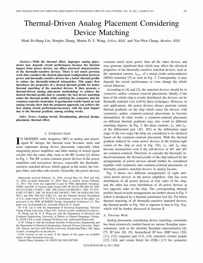
Fig. 4 shows two different arrangements of eight unit-sized power devices in the power amplifiers. One has evendistribution of all power devices at four sides of the chip,and the other has even distribution of all power devices attwo opposite sides of the chip. The corresponding thermalprofiles based on both arrangements are further shown in Fig. 5which is produced by a thermal simulation tool [6]. For betterthermal matching of all thermally-sensitive matched devices,the thermal profile in Fig. 5(b) is superior to that in Fig. 5(a),which will be further discussed in Section II.
A. Previous Work
Analog placement considering device matching constraintshas been extensively studied based on various floorplan repre-sentations, such as the absolute floorplan representation [4],[7], B*-tree [8], [9], hierarchical B*-tree (HB*-tree) [10],[11], [12], sequence pair [13], [14], transitive closure graphs[15], [16], and corner block list (CBL) [17] for symmetry
0278-0070/$26.00 c© 2011 IEEE
326 IEEE TRANSACTIONS ON COMPUTER-AIDED DESIGN OF INTEGRATED CIRCUITS AND SYSTEMS, VOL. 30, NO. 3, MARCH 2011
Fig. 1. Block diagram of a generic RF system [2].
Fig. 2. Idsat versus temperature of a MOS transistor [3].
Fig. 3. (a) Schematic of a two-stage Op-Amp. (b) Common-centroid place-ment of the differential pair (M1, M2) in (a) with the thermal gradient inducedby some power devices at the bottom-right corner of the chip.
constraints, and CBL and grid-based approaches [18] forcommon-centroid constraints. Among these works, only [4],[7], and [17] addressed thermally constrained symmetric place-ment.
Cohn et al. [4] introduced a basic placement configurationfor thermal device matching, which is to position the powerdevices along a thermal symmetry line bisecting the chipsuch that the isothermal contours are symmetric across thesymmetry line. The thermally-sensitive matched devices arethen placed symmetrically about the power devices to havethe same ambient temperature. Consequently, the thermalmismatch between the matched devices is reduced. Althoughsuch an approach is very effective, it limits the layout designwith only one symmetry line on the chip. Such a configurationfor thermal device matching is not applicable to modern RFor analog and mixed-signal design as seen in Fig. 1, whichcontains multiple symmetry groups with different symmetrylines in different sub-circuits.
Both Lampaert et al. [7] and Liu et al. [17], [19] presentedtheir thermally constrained analog placement approaches by
Fig. 4. (a) All power devices are evenly distributed at four sides of the chip.(b) All power devices are evenly distributed at two opposite sides of the chip.
Fig. 5. Thermal profiles based on two kinds of power device arrangements.(a) Thermal profile where power devices are evenly distributed at four sidesof the chip. (b) Thermal profile where power devices are evenly distributedat two opposite sides of the chip.
thermal profile computations. During placement iterations,the temperature of all matched devices is calculated basedon a certain thermal model. The thermally-induced mismatchis then optimized by minimizing the temperature differencesbetween the symmetric devices. Although their approachesdo not limit the layout with only one symmetry line, it istime-consuming to calculate the temperature of all matcheddevices during placement iterations when the number ofthe matched devices is large. In addition, it is difficult toguarantee that all devices are thermally matched by summingup the temperature differences between symmetric devices ineach symmetry group and other placement objectives suchas reducing placement area and thermal hot spots [17]. Noneof the previous works directly optimizes the thermal profilebased on the power device arrangement to achieve betterthermal matching of the devices.
B. Our Contributions
In this paper, we propose the first thermal-driven analogplacement considering thermal device matching by directlyoptimizing the thermal profile of analog layouts. We introducethe desired thermal profile and the corresponding placementconfiguration for better device matching, especially whenplacing multiple symmetry groups with different symmetrylines. We then present our placement methodology to si-multaneously place all devices, including power devices andthermally-sensitive matched devices with either the symmetryor the common-centroid constraint. We adopt a table-lookupapproach to speed up the thermal profile computation. Thethermal profile is optimized based on coarse-grid and fine-grid thermal tables at different placement stages. Since theobjective based on our approach is to generate the desired
LIN et al.: THERMAL-DRIVEN ANALOG PLACEMENT CONSIDERING DEVICE MATCHING 327
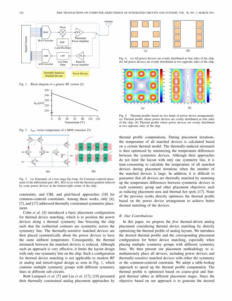
Fig. 6. (a) 3-D thermal profile of the non-power device area in Fig. 5(a).(b) 3-D thermal profile of the non-power device area in Fig. 5(b).
thermal profile, instead of to minimize the temperature differ-ences between matched devices, the time complexity is onlydependent on the number of power devices, but is independentof that of matched devices. Therefore, our approach is moreefficient and scalable, which significantly improves the runtimewhen placing a large number of thermally-sensitive matcheddevices in modern analog designs. Finally, we propose thefirst thermal-driven common-centroid placement (TCCP) al-gorithm that considers the best device matching under thedesired thermal profile. Experimental results show that ourapproach can achieve better runtime and the best analog circuitperformance/accuracy in the presence of thermal gradients,compared with the previous works.
The remainder of this paper is organized as follows.Section II introduces the desired thermal profile for thermaldevice matching and the corresponding placement configura-tion. Section III presents our thermal-driven analog placementto generate the desired thermal profile based on the placementconfiguration while considering both symmetry and common-centroid constraints. Section IV reports the experimental re-sults, and finally Section V concludes this paper.
II. The Desired Thermal Profile
Before introducing our thermal-driven analog placement,we shall first consider the desired thermal profiles and thecorresponding placement configuration. Inspired by manuallayouts, the desired thermal profile should have the followingproperties:
1) lower temperature at thermal hot spots;2) smoother thermal gradients at the non-power device
areas;3) more separation between power and thermally-sensitive
devices;4) more regular isothermal contours in either the horizontal
or the vertical direction such that the matched devicescan easily be placed along the contours;
5) larger accommodation areas for multiple thermally-sensitive device groups.
Fig. 6 further shows the 3-D thermal profiles of the non-power device area in Fig. 5. By comparing both thermalprofiles at the non-power device areas in Fig. 6, although theone that the power devices are evenly distributed at four sidesof the chip has lower temperature at the thermal hot spots,its thermal gradient, isothermal contours, and accommodation
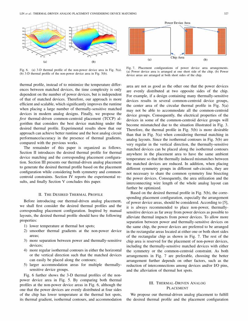
Fig. 7. Placement configurations of power device area arrangements.(a) Power device area is arranged at one short side of the chip. (b) Powerdevice areas are arranged at both short sides of the chip.
area are not as good as the other one that the power devicesare evenly distributed at two opposite sides of the chip.For example, if a design containing many thermally-sensitivedevices results in several common-centroid device groups,the center area of the circular thermal profile in Fig. 5(a)may not be able to accommodate all the common-centroiddevice groups. Consequently, the electrical properties of thedevices in some of the common-centroid device groups willbecome mismatched due to the situation illustrated in Fig. 3.Therefore, the thermal profile in Fig. 5(b) is more desirablethan that in Fig. 5(a) when considering thermal matching inanalog layouts. Since the isothermal contours in Fig. 5(b) arevery regular in the vertical direction, the thermally-sensitivematched devices can be placed along the isothermal contoursanywhere in the placement area to have the same ambienttemperature so that the thermally induced mismatches betweenthe matched devices are reduced. In addition, when placingdifferent symmetry groups in different sub-circuits, they arenot necessary to share the common symmetry line bisectingthe power devices. Consequently, the area utilization and theinterconnecting wire length of the whole analog layout canfurther be optimized.
Based on the desired thermal profile in Fig. 5(b), the corre-sponding placement configuration, especially the arrangementof power device areas, should be considered. According to [5],it is always recommended to place non-power, thermally-sensitive devices as far away from power devices as possible toalleviate thermal impacts from power devices. To allow moreseparation between power and thermally-sensitive devices onthe same chip, the power devices are preferred to be arrangedin the rectangular areas located at either one or both short sidesof the rectangular chip as shown in Fig. 7. The rest of thechip area is reserved for the placement of non-power devices,including the thermally-sensitive matched devices with eitherthe symmetry or the common-centroid constraint. As botharrangements in Fig. 7 are preferable, choosing the betterarrangement further depends on other factors, such as thereduction of interconnections among devices and/or I/O pins,and the alleviation of thermal hot spots.
III. Thermal-Driven Analog
Placement
We propose our thermal-driven analog placement to fulfillthe desired thermal profile and the placement configuration
328 IEEE TRANSACTIONS ON COMPUTER-AIDED DESIGN OF INTEGRATED CIRCUITS AND SYSTEMS, VOL. 30, NO. 3, MARCH 2011
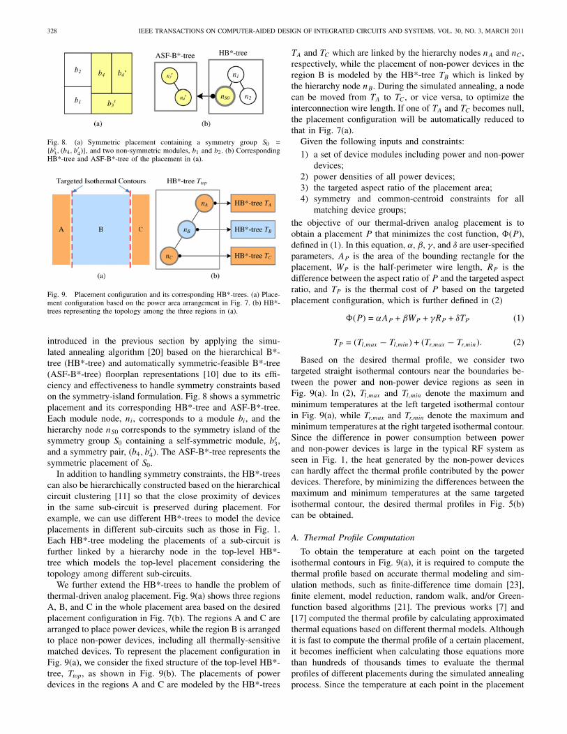
Fig. 8. (a) Symmetric placement containing a symmetry group S0 ={bs
3, (b4, b′4)}, and two non-symmetric modules, b1 and b2. (b) Corresponding
HB*-tree and ASF-B*-tree of the placement in (a).
Fig. 9. Placement configuration and its corresponding HB*-trees. (a) Place-ment configuration based on the power area arrangement in Fig. 7. (b) HB*-trees representing the topology among the three regions in (a).
introduced in the previous section by applying the simu-lated annealing algorithm [20] based on the hierarchical B*-tree (HB*-tree) and automatically symmetric-feasible B*-tree(ASF-B*-tree) floorplan representations [10] due to its effi-ciency and effectiveness to handle symmetry constraints basedon the symmetry-island formulation. Fig. 8 shows a symmetricplacement and its corresponding HB*-tree and ASF-B*-tree.Each module node, ni, corresponds to a module bi, and thehierarchy node nS0 corresponds to the symmetry island of thesymmetry group S0 containing a self-symmetric module, bs
3,and a symmetry pair, (b4, b
′4). The ASF-B*-tree represents the
symmetric placement of S0.In addition to handling symmetry constraints, the HB*-trees
can also be hierarchically constructed based on the hierarchicalcircuit clustering [11] so that the close proximity of devicesin the same sub-circuit is preserved during placement. Forexample, we can use different HB*-trees to model the deviceplacements in different sub-circuits such as those in Fig. 1.Each HB*-tree modeling the placements of a sub-circuit isfurther linked by a hierarchy node in the top-level HB*-tree which models the top-level placement considering thetopology among different sub-circuits.
We further extend the HB*-trees to handle the problem ofthermal-driven analog placement. Fig. 9(a) shows three regionsA, B, and C in the whole placement area based on the desiredplacement configuration in Fig. 7(b). The regions A and C arearranged to place power devices, while the region B is arrangedto place non-power devices, including all thermally-sensitivematched devices. To represent the placement configuration inFig. 9(a), we consider the fixed structure of the top-level HB*-tree, Ttop, as shown in Fig. 9(b). The placements of powerdevices in the regions A and C are modeled by the HB*-trees
TA and TC which are linked by the hierarchy nodes nA and nC,respectively, while the placement of non-power devices in theregion B is modeled by the HB*-tree TB which is linked bythe hierarchy node nB. During the simulated annealing, a nodecan be moved from TA to TC, or vice versa, to optimize theinterconnection wire length. If one of TA and TC becomes null,the placement configuration will be automatically reduced tothat in Fig. 7(a).
Given the following inputs and constraints:
1) a set of device modules including power and non-powerdevices;
2) power densities of all power devices;3) the targeted aspect ratio of the placement area;4) symmetry and common-centroid constraints for all
matching device groups;
the objective of our thermal-driven analog placement is toobtain a placement P that minimizes the cost function, �(P),defined in (1). In this equation, α, β, γ , and δ are user-specifiedparameters, AP is the area of the bounding rectangle for theplacement, WP is the half-perimeter wire length, RP is thedifference between the aspect ratio of P and the targeted aspectratio, and TP is the thermal cost of P based on the targetedplacement configuration, which is further defined in (2)
�(P) = αAP + βWP + γRP + δTP (1)
TP = (Tl,max − Tl,min) + (Tr,max − Tr,min). (2)
Based on the desired thermal profile, we consider twotargeted straight isothermal contours near the boundaries be-tween the power and non-power device regions as seen inFig. 9(a). In (2), Tl,max and Tl,min denote the maximum andminimum temperatures at the left targeted isothermal contourin Fig. 9(a), while Tr,max and Tr,min denote the maximum andminimum temperatures at the right targeted isothermal contour.Since the difference in power consumption between powerand non-power devices is large in the typical RF system asseen in Fig. 1, the heat generated by the non-power devicescan hardly affect the thermal profile contributed by the powerdevices. Therefore, by minimizing the differences between themaximum and minimum temperatures at the same targetedisothermal contour, the desired thermal profiles in Fig. 5(b)can be obtained.
A. Thermal Profile Computation
To obtain the temperature at each point on the targetedisothermal contours in Fig. 9(a), it is required to compute thethermal profile based on accurate thermal modeling and sim-ulation methods, such as finite-difference time domain [23],finite element, model reduction, random walk, and/or Green-function based algorithms [21]. The previous works [7] and[17] computed the thermal profile by calculating approximatedthermal equations based on different thermal models. Althoughit is fast to compute the thermal profile of a certain placement,it becomes inefficient when calculating those equations morethan hundreds of thousands times to evaluate the thermalprofiles of different placements during the simulated annealingprocess. Since the temperature at each point in the placement
LIN et al.: THERMAL-DRIVEN ANALOG PLACEMENT CONSIDERING DEVICE MATCHING 329
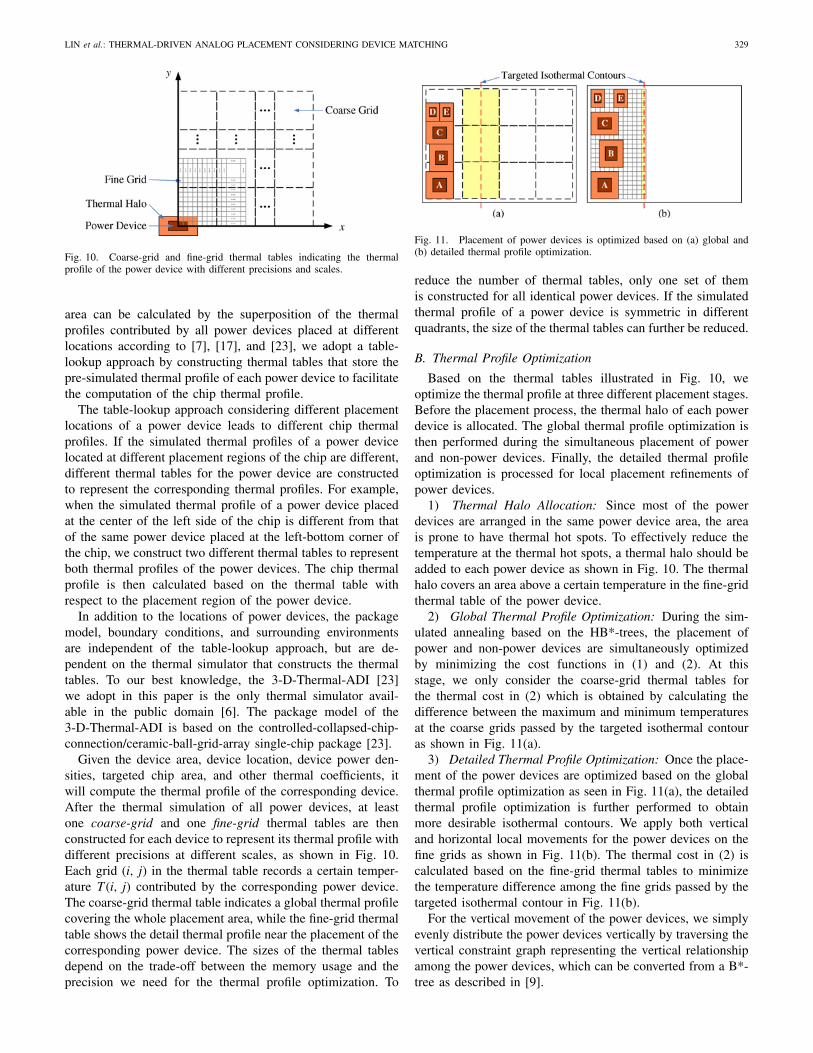
Fig. 10. Coarse-grid and fine-grid thermal tables indicating the thermalprofile of the power device with different precisions and scales.
area can be calculated by the superposition of the thermalprofiles contributed by all power devices placed at differentlocations according to [7], [17], and [23], we adopt a table-lookup approach by constructing thermal tables that store thepre-simulated thermal profile of each power device to facilitatethe computation of the chip thermal profile.
The table-lookup approach considering different placementlocations of a power device leads to different chip thermalprofiles. If the simulated thermal profiles of a power devicelocated at different placement regions of the chip are different,different thermal tables for the power device are constructedto represent the corresponding thermal profiles. For example,when the simulated thermal profile of a power device placedat the center of the left side of the chip is different from thatof the same power device placed at the left-bottom corner ofthe chip, we construct two different thermal tables to representboth thermal profiles of the power devices. The chip thermalprofile is then calculated based on the thermal table withrespect to the placement region of the power device.
In addition to the locations of power devices, the packagemodel, boundary conditions, and surrounding environmentsare independent of the table-lookup approach, but are de-pendent on the thermal simulator that constructs the thermaltables. To our best knowledge, the 3-D-Thermal-ADI [23]we adopt in this paper is the only thermal simulator avail-able in the public domain [6]. The package model of the3-D-Thermal-ADI is based on the controlled-collapsed-chip-connection/ceramic-ball-grid-array single-chip package [23].
Given the device area, device location, device power den-sities, targeted chip area, and other thermal coefficients, itwill compute the thermal profile of the corresponding device.After the thermal simulation of all power devices, at leastone coarse-grid and one fine-grid thermal tables are thenconstructed for each device to represent its thermal profile withdifferent precisions at different scales, as shown in Fig. 10.Each grid (i, j) in the thermal table records a certain temper-ature T (i, j) contributed by the corresponding power device.The coarse-grid thermal table indicates a global thermal profilecovering the whole placement area, while the fine-grid thermaltable shows the detail thermal profile near the placement of thecorresponding power device. The sizes of the thermal tablesdepend on the trade-off between the memory usage and theprecision we need for the thermal profile optimization. To
Fig. 11. Placement of power devices is optimized based on (a) global and(b) detailed thermal profile optimization.
reduce the number of thermal tables, only one set of themis constructed for all identical power devices. If the simulatedthermal profile of a power device is symmetric in differentquadrants, the size of the thermal tables can further be reduced.
B. Thermal Profile Optimization
Based on the thermal tables illustrated in Fig. 10, weoptimize the thermal profile at three different placement stages.Before the placement process, the thermal halo of each powerdevice is allocated. The global thermal profile optimization isthen performed during the simultaneous placement of powerand non-power devices. Finally, the detailed thermal profileoptimization is processed for local placement refinements ofpower devices.
1) Thermal Halo Allocation: Since most of the powerdevices are arranged in the same power device area, the areais prone to have thermal hot spots. To effectively reduce thetemperature at the thermal hot spots, a thermal halo should beadded to each power device as shown in Fig. 10. The thermalhalo covers an area above a certain temperature in the fine-gridthermal table of the power device.
2) Global Thermal Profile Optimization: During the sim-ulated annealing based on the HB*-trees, the placement ofpower and non-power devices are simultaneously optimizedby minimizing the cost functions in (1) and (2). At thisstage, we only consider the coarse-grid thermal tables forthe thermal cost in (2) which is obtained by calculating thedifference between the maximum and minimum temperaturesat the coarse grids passed by the targeted isothermal contouras shown in Fig. 11(a).
3) Detailed Thermal Profile Optimization: Once the place-ment of the power devices are optimized based on the globalthermal profile optimization as seen in Fig. 11(a), the detailedthermal profile optimization is further performed to obtainmore desirable isothermal contours. We apply both verticaland horizontal local movements for the power devices on thefine grids as shown in Fig. 11(b). The thermal cost in (2) iscalculated based on the fine-grid thermal tables to minimizethe temperature difference among the fine grids passed by thetargeted isothermal contour in Fig. 11(b).
For the vertical movement of the power devices, we simplyevenly distribute the power devices vertically by traversing thevertical constraint graph representing the vertical relationshipamong the power devices, which can be converted from a B*-tree as described in [9].

330 IEEE TRANSACTIONS ON COMPUTER-AIDED DESIGN OF INTEGRATED CIRCUITS AND SYSTEMS, VOL. 30, NO. 3, MARCH 2011
Algorithm 1 Detailed Thermal Profile Optimization
1: Evenly distribute the power devices in the vertical direc-tion;
2: Calculate TP ;3: repeat4: for all boundary power devices do5: for all valid horizontal movements do6: Calculate TP ;7: end for8: Move the power device to the position that minimizes
TP ;9: Update TP ;
10: end for11: until TP cannot further be reduced.
Fig. 12. (a) BJT differential pair (Q1, Q2). (b) Thermal-driven symmetricplacement of the differential pair. The horizontal dotted lines denote theisothermal contours, while the vertical one denotes the symmetry axis.
For the horizontal movement of the power devices, tominimize the number of power devices that need to be moved,only those adjacent to the right boundary of the power devicearea should be considered, which are devices A, B, C, andE in Fig. 11(a). These boundary devices can be identified bythe contour data structure during packing a B*-tree [24]. Bythe iterative horizontal movement of the boundary devices asshown in Algorithm 1, the thermal cost TP in (2) can furtherbe minimized.
C. Thermal-Driven Matching Device Placement
We consider the desired thermal profile in Fig. 5(b) toplace the thermally-sensitive matched devices with either thesymmetry or the common-centroid constraint.
1) Thermal-Driven Symmetric Placement: For a matchingdevice group with the symmetry constraint, the matched de-vices should be placed on the same isothermal contours to havethe same ambient temperature so that the thermally-inducedmismatch is minimized. Since the desired thermal profile hasregular isothermal contours in either the horizontal or thevertical direction, all the symmetry device groups can simplybe placed with their symmetry axes being perpendicular tothe isothermal contours. The symmetric placements of allsymmetry device groups with different symmetry axes cansimultaneously be optimized during the simulated annealingbased on the HB*-trees. Fig. 12(b) shows the thermal-drivensymmetric placement of the BJT differential pair in Fig. 12(a)with the symmetry axis being perpendicular to the horizontalisothermal contours.
2) Thermal-Driven Common-Centroid Placement: For amatching device group with the common-centroid constraint
Fig. 13. Matching device group with the common-centroid constraint.(a) Matching device group in the binary weighted current network.(b) Thermal-driven common-centroid placement of the matching device groupin (a) containing four MOS devices, A, B, C, and D, having 4, 4, 8, and 16sub-devices, respectively. The horizontal dotted lines denote the isothermalcontours.
as shown in Fig. 13, none of the previous works considersthe thermal profile during the common-centroid placement.We propose our algorithm to generate a common-centroidplacement for a matching device group while considering thedesired thermal profile. Based on our approach, all possiblecommon-centroid placements of each matching group withdifferent aspect ratios (i.e., different numbers of transistorrows) are pre-generated, which is the same as the approachin [18]. When integrating the placement with other devicesor device groups, a candidate of the pre-generated common-centroid placements is randomly selected during the simulatedannealing based on the HB*-trees. The final candidates of allmatching groups are simultaneously optimized based on thecost function in (1).
Given a common-centroid device group Gcc containing q
devices, i.e., Gcc = {b1, b2, . . . , bq}, and each device bj hasnbj
sub-devices, to better match the device layouts, the sizeof all the sub-devices should be identical. Besides, in Gcc, therelationship between any two sub-device numbers nbj
and nbk
of devices bj and bk is usually the ratio of power of two, i.e.,nbj
= 2l × nbk, where l is an integer. Furthermore, the sub-
devices are preferred to be regularly placed in a 2-D arrayas shown in Fig. 13(b). To minimize the thermal mismatchamong the q devices in Gcc, we need to evenly distribute thesub-devices of each device along the direction of the thermalgradient.
Fig. 13(b) shows the thermal-driven common-centroidplacement of the 3-bit binary weighted current network il-lustrated in Fig. 13(a). Device A denotes the MOS transistorconnected to Iin, and devices B, C, D denote the MOStransistors connected to the control signals of B3, B2, andB1, which have 4, 4, 8, and 16 sub-devices, respectively. Theisothermal contours, i.e., the dotted lines, are in the horizontal
LIN et al.: THERMAL-DRIVEN ANALOG PLACEMENT CONSIDERING DEVICE MATCHING 331
direction, implying that the direction of the thermal gradientis vertical. In the following, we simply consider the directionof the row (column) of the 2-D array to be the same as thatof the thermal gradient (contours).
To assign the sub-devices into a k-row 2-D array whileminimizing the thermal mismatch, the sub-devices of eachdevice should be equally divided by k and assigned into oneof the rows. For some cases, if the sub-device number of adevice is not dividable with respect to the row number, weallow the sub-device number in each row with ±1 tolerance.It should be noted that even the sub-device numbers of a deviceassigned to different rows are not equal, the sub-device numberin the ith row should be the same as that in the (k − i + 1)throw, or the symmetric row. Therefore, the common-centroidplacement must be feasible. In Fig. 13(b), the respective sub-device numbers of devices A, B, C, and D in each row are 1,1, 2, 4 after the even assignment.
Once the sub-devices of each device are evenly assignedinto rows, we should consider the diffusion-sharing for MOStransistors. We construct the diffusion graph of the sub-circuitin each row, and then find the Eulerian trail on the diffusiongraph [25]. After the Eulerian trails are found, the sub-deviceson the same Eulerian trail are merged. Considering the firstrow in Fig. 13(b), there are three Eulerian trails, C−C, D−D,and D−D. Consequently, the six devices are merged into threesub-device groups, and the sub-devices in the symmetric roware also merged accordingly.
After considering the diffusion sharing, the column positionof each sub-device or sub-device group in each row is assignedin a random order while keeping the symmetric row in thereverse order. Fig. 13(b) shows the final common-centroidplacement that minimizes the mismatch between the fourdevices due to the thermal gradient. The algorithm of thek-row thermal-driven common-centroid placement (namely,k-row TCCP) is summarized in Algorithm 2.
To ensure that all q devices in Gcc share a common centroid,the sub-device number of each device should be even, orat most one of the devices contains an odd number of sub-devices [18]. If there is a device containing an odd numberof sub-devices in Gcc, the number of rows, k, must be oddto ensure a common-centroid placement of Gcc. Our k-rowTCCP algorithm can handle the common-centroid placementwith both even and odd numbers of rows as illustrated inAlgorithm 2.
IV. Experimental Results
We implemented our placement algorithm in the C++ pro-gramming language on a Dual 2.8 GHz Intel Pentium4 PCunder the Linux operation system. We performed two sets ofexperiments: 1) thermal-driven analog placement consideringsymmetry constraints, and 2) thermal-driven common-centroidplacement.
A. Thermal-Driven Analog Placement with SymmetryConstraints
In the first set of the experiments, we adapted the ana-log placement benchmarks used in [8], [9], [10], [12], and
Algorithm 2 k-row TCCP
1: for all q devices in Gcc do2: if the sub-device number is odd then3: Assign one sub-device into the middle row;4: Evenly assign the rest of the sub-device into k rows
with the same number in row[i] and row[k − i + 1];5: else6: Evenly assign the sub-devices into k rows with the
same number in row[i] and row[k − i + 1];7: end if8: end for9: for i = 1 to �k/2� do
10: if k is odd and i is equal to �k/2� then11: if the middle position in row[i] is occupied then12: Place a sub-device of the device with an odd
number of sub-devices at a position closest to themiddle position in row[i];
13: else14: Place a sub-device of the device with an odd
number of sub-devices at the middle position inrow[i];
15: end if16: Divide the rest of the sub-devices into two partitions
in which the sub-device numbers of each device arethe same;
17: Merge the diffusion of the sub-devices in each parti-tion based on the same Eulerian trails;
18: Place the (merged) sub-devices in one partition onthe left side of row[i] in a random order;
19: Place the (merged) sub-devices in the other partitionon the right side of row[i] with a mirrored placementof the sub-devices on the left side of row[i];
20: else21: Merge the diffusion of the sub-devices in row[i] and
row[k − i + 1] based on the same Eulerian trails;22: Place the (merged) sub-devices in row[i] in a random
order;23: Place the (merged) sub-devices in row[k − i + 1] in
the reverse order of that in row[i];24: end if25: end for
[13] consisting of two analog designs, biasynth 2p4g andlnamixbias 2p4g, with different numbers of device modulesand symmetry groups. Since there was no power devicespecified in the original benchmarks, in each design, a numberof device modules were considered as power devices whichhave much higher power densities (� 1015 W/m3), such thatthe ratio between high-power and other device areas is approx-imately 1:10, based on the typical design in Fig. 1. Table I liststhe names of the benchmark circuits (“Circuit”), the numbersof modules (“# of Mod.”), the numbers of symmetry modules(“# of Sym. Mod.”), the numbers of power device modules (“#of Power Mod.”), and the total module areas (“Mod. Area”).
We compared the analog placement approaches with andwithout considering the thermal effect as reported in Table II.For the analog placement approaches without considering the

332 IEEE TRANSACTIONS ON COMPUTER-AIDED DESIGN OF INTEGRATED CIRCUITS AND SYSTEMS, VOL. 30, NO. 3, MARCH 2011
TABLE I
Benchmark Circuits with Different Numbers of Device
Modules
# of # of # of Mod.Circuit Mod. Sym. Power Area
Mod. Mod. (103 µm2)biasynth 2p4g 65 8+12+5 11 4.70lnamixbias 2p4g 110 16+6+6+12+4 10 46.00
thermal effect, two state-of-the-art analog placement tools inthe literature, SymmetryIsland [10], [12] and Plantage [9],are compared. For analog placement approaches consideringthe thermal effect, we compared the proposed approach thatoptimizes the desired thermal profile with the other one thatminimizes the temperature differences between devices ofeach symmetry pair. Both approaches applied the simulatedannealing algorithm with the same annealing schedule basedon the HB*-trees and the cost function in (1), while thelater one applied a different thermal cost function TP ofplacement P defined in (3), which is the summation of thetemperature difference of m symmetry pairs. In (3), Tbi
denotesthe temperature of the device bi, and Tbi,sym
corresponds thetemperature of the symmetric device of bi
TP =m∑i=1
|Tbi− Tbi,sym
|. (3)
To balance the costs of the four placement objectives, AP , WP ,RP , and TP (or TP ), with the same coefficients, α, β, γ , andδ, in (1) for different analog designs, we shall first randomlysearch N placement solutions based on the HB*-trees beforesimulated annealing. The maximum and minimum costs ofeach placement objective based on the N placement solutionsare then recorded to normalize the values of AP , WP , RP , andTP (or TP ) between 0 and 1. Consequently, (1) is calculatedbased on the normalized costs during the simulated annealing,and the coefficients, α, β, γ , and δ, do not need to be changedfrom design to design.
Table II lists the total areas (“Area”) and the runtimes(“Time”) for both approaches, SymmetryIsland [10], [12] andPlantage [9], without considering the thermal effect (“WithoutThermal Effect”), and the maximum temperature of the wholechip (“TMax”), the maximum temperature difference of eachsymmetry pair (“Max �Tsym”), the total areas (“Area”) andthe runtimes (“Time”) for both approaches, the temperaturedifference optimization (“Temperature Diff. Opt.”) and thethermal profile optimization (“Thermal Profile Opt.”), withconsidering the thermal effect (“With Thermal Effect”). Theapproaches, SymmetryIsland [10], [12] and Plantage [9], wereperformed on a Pentium4 3.2 GHz PC, while the other twoapproaches based on the temperature difference optimizationand the thermal profile optimization were performed on aPentium4 Dual 2.8 GHz PC.
When comparing the total areas and runtimes among thefour approaches, the total areas generated by Symmetry-Island [10], [12] and Plantage [9] are 11% smaller thanthose generated by the approaches considering the thermaleffect. In addition to smaller chip areas, the runtimes of
Fig. 14. (a) Resulting placement of lnamixbias 2p4g based on the proposedthermal profile optimization. (b) Corresponding thermal profile of the resultingplacement in (a).
SymmetryIsland [10], [12] and Plantage are shorter. Therefore,considering the thermal effect would inevitably incur penaltieson both chip area and running time. For the comparisonsof the analog placement approaches considering the thermaleffect, our proposed approach results in less than one quartertemperature difference of the matched devices in a symmetrypair and 5.28X faster running time with comparable maximumchip temperature and total chip area.
Fig. 14 shows the resulting placement of lnamixbias 2p4gbased on the proposed thermal profile optimization and its cor-responding thermal profile. The heavily shaded device moduleson the left boundary of the chip region are the power devices,and all the other shaded device modules denote symmetricdevices. Fig. 15 further shows the resulting placement oflnamixbias 2p4g based on the temperature difference opti-mization and its corresponding thermal profile for comparison.In Fig. 15, the symmetric devices which are not placed on thesame isothermal contours result in higher device mismatchesdue to the thermal effect.
To demonstrate the effectiveness of the proposed approach,we further performed the experiment based on the circuit“lnamixbias 2p4g” with different numbers of power devicesranging from 5 to 30. Table III shows the comparisons of“TMax,” “Max �Tsym,” and “Area (Percentage of dead space)”based on the two different analog placement approaches. Theresults show that our approach achieves the best thermal

LIN et al.: THERMAL-DRIVEN ANALOG PLACEMENT CONSIDERING DEVICE MATCHING 333
TABLE II
Comparisons of Analog Placement Approaches With and Without Considering the Thermal Effect
Without Thermal Effect With Thermal EffectSymmetryIsland Plantage Temperature Diff. Opt. Thermal Profile Opt.
[10], [12] [9] (This Paper)Circuit (Pentium4 3.2 GHz) (Pentium4 3.2 GHz) (Pentium4 Dual 2.8 GHz) (Pentium4 Dual 2.8 GHz)
Area Time Area Time TMax Max Area Time TMax Max Area Time�Tsym �Tsym
(103 µm2) (s) (103 µm2) (s) (K) (K) (103 µm2) (s) (K) (K) (103 µm2) (s)biasynth 2p4g 4.92 22 4.93 337 318.18 0.91 5.42 1524 321.10 0.22 5.47 385lnamixbias 2p4g 48.63 43 49.53 387 322.58 2.66 56.71 5340 322.09 0.62 55.87 809Comparison 0.88 – 0.89 – 1.00 4.21 1.00 5.28 1.00 1.00 1.00 1.00
TABLE III
Comparisons of TMax , Max �Tsym , and Area (Percentage of Dead Space) Based on Different
Analog Placement Approaches
# of Temperature Diff. Opt. Thermal Profile Opt. (This Paper)Circuit Power TMax Max �Tsym Dead Space TMax Max �Tsym Dead Space
Mod. (K) (K) (%) (K) (K) (%)lnamixbias 2p4g 5 310.39 0.52 15.80 310.41 0.01 15.08lnamixbias 2p4g 10 322.58 2.66 18.89 322.09 0.62 17.67lnamixbias 2p4g 15 345.25 1.61 19.04 345.63 0.12 16.92lnamixbias 2p4g 20 345.30 2.07 23.84 345.93 0.07 18.52lnamixbias 2p4g 25 346.10 2.67 20.14 345.95 0.33 17.55lnamixbias 2p4g 30 347.15 1.70 20.64 346.10 0.68 16.25
Comparison 1.00 18.31 1.16 1.00 1.00 1.00
matching of symmetric devices without degrading TMax andchip area when the number of power devices increase.
B. Thermal-Driven Common-Centroid Placement
Similar to the approach in [18], our thermal-driven analogplacement based on the HB*-trees generates and stores allpossible common-centroid configurations with different rownumbers for each common-centroid device group, and thesimulated-annealing algorithm selects the best configurationfor each group to minimize the total chip area. We performedthe second set of the experiments to compare the matchingproperties of different device placements within a common-centroid group with the same placement dimensions and samethermal profile.
The second set of the experiments is based on the realanalog circuit, the binary weighted current network as shownin Fig. 13(a), containing a large common-centroid devicegroup in which each device has different numbers of sub-devices in uniform sizes. We experimented on five benchmarkcircuits of the binary weighted current network ranging fromfour bits to eight bits. Table V lists the names of the benchmarkcircuits (“Circuit”), the numbers of devices (“# of Dev.”), andthe number of sub-devices in each device (“# of Sub-devices”).
In this experiment, the thermally-induced mismatch withina common-centroid placement of the binary-weighted currentnetwork is evaluated under the desired thermal profile, as seenin Fig. 5(b), by performing HSPICE simulation with pre-assigned temperature for each sub-device. The temperatureof each sub-device in the common-centroid group can beextracted according to its location in the thermal profile oncethe whole common-centroid device group is placed at a certainposition in region B in Fig. 9(a). After performing HSPICE
Fig. 15. (a) Resulting placement of lnamixbias 2p4g based on the tempera-ture difference optimization. (b) Corresponding thermal profile of the resultingplacement in (a).
334 IEEE TRANSACTIONS ON COMPUTER-AIDED DESIGN OF INTEGRATED CIRCUITS AND SYSTEMS, VOL. 30, NO. 3, MARCH 2011
TABLE IV
Benchmark Circuits of Binary-Weighted Current Network
with Different Bit Numbers
Circuit # of Dev. # of Sub-Devicesbwcn 4bit 5 {4, 4, 8, 16, 32}bwcn 5bit 6 {4, 4, 8, 16, 32, 64}bwcn 6bit 7 {4, 4, 8, 16, 32, 64, 128}bwcn 7bit 8 {4, 4, 8, 16, 32, 64, 128, 256}bwcn 8bit 9 {4, 4, 8, 16, 32, 64, 128, 256, 512}
TABLE V
Comparisons of the Circuit Accuracy Due to
Thermally-Induced Mismatches for Common-Centroid
Placements Based on the Grid-Based Approach and Our k-Row
TCCP Algorithm
Average σ ValueCircuit The Grid-Based Approach [18] TCCP
Method 1 Method 2 Method 3bwcn 4bit 0.06784 0.07040 0.04480 0.00128bwcn 5bit 0.26624 0.28416 0.00512 0.00512bwcn 6bit 1.06496 1.13664 0.73728 0.04096bwcn 7bit 4.24960 4.50560 0.06144 0.20480bwcn 8bit 16.9984 18.14528 11.81696 0.43008
The numbers in bold font mean that the circuits are within the toleranceof the accuracy.
simulation, the temperature-dependent electrical parameters ofeach device were measured. Since our experiment is basedon the binary weighted current network in Fig. 13(a), whichis commonly used in data converter systems, we measuredthe drain current ID of each MOS transistor. For an n-bitdata converter system, the ID linearity may change maxi-mally by ± 1
4 LSB over the full temperature range to maintainmonotonicity of the system, where LSB stands for the leastsignificant bit in data converters [26]. If the difference betweenthe ideal ID and the real one, I ′
D, is larger than ± 14 LSB, the
D/A converter will fail. If the thermally-induced mismatchvalue, σ, of a common-centroid placement shown in (4) is lessthan one, the circuit is within the tolerance of the accuracy;otherwise, the circuit will fail
σ =|I ′
D − ID|14LSB
. (4)
Therefore, we compared the σ value of the resulting common-centroid placement based on our k-row TCCP algorithm withthat based on the grid-based approach in [18] under thesame ambient temperature or the same location in the thermalprofile.
Table V lists the names of the benchmark circuits (“Cir-cuit”), and the σ values based on the grid-based approach [18]and our k-row TCCP algorithm. Methods 1–3 give three dif-ferent assignments of the positions of the sub-devices based onthe grid-based approach [18]. For Method 1 (Method 2), thedevices containing the most (least) sub-devices were assignedfirst, so they were placed close to the centroid. For Method 3,the sub-devices were assigned in a random order. For fairercomparisons, we calculated the average σ values of 100different common-centroid placements of each circuit based
Fig. 16. Resulting placements of the common-centroid group in the 4-bit binary weighted current network containing five devices, where eachdevice has 16, 16, 32, 64, and 128 sub-devices, respectively. (a) Method 1.(b) Method 2. (c) Method 3. (d) Our k-row TCCP algorithm.
on Method 3 and the proposed k-row TCCP algorithm. Theresults show that our k-row TCCP algorithm obtained accurateresults for all the bwcn circuits. Fig. 16 shows the abstract viewof the resulting 8-row placements for the common-centroidgroup in the 4-bit binary weighted current network with fivedevices, where each device has 16, 16, 32, 64, and 128 sub-devices, respectively. The devices, m5, containing the mostsub-devices are placed in the middle rows (from the third tosixth rows) based on Method 1 as shown in Fig. 16(a), whilethey are placed in the outer rows (the first, second, seventh,and eighth rows) based on Method 2 as shown in Fig. 16(b).Fig. 16(c) shows the resulting placement based on Method 3,where all sub-devices are randomly distributed in all rows, andFig. 16(d) shows the resulting placement based on our k-rowTCCP algorithm.
As seen in Table V, the results based on “Method 3” arenot as good as ours when the device/sub-device number inthe common centroid group becomes larger. Both Methods 1and 2 have very poor performance against the impact from thethermal gradient since only small circuits behave accurately.Therefore, our approach is the most effective one that consid-ers the thermal gradient. The runtime of every approach hereis less than one second on a Dual 2.8 GHz P4 PC.
V. Conclusion
In this paper, we addressed the thermal issue in analogplacement and studied the thermal-driven analog placement

LIN et al.: THERMAL-DRIVEN ANALOG PLACEMENT CONSIDERING DEVICE MATCHING 335
problem. We proposed our algorithms to simultaneouslyoptimize the placements of power and non-power devicesto generate a desired thermal profile for thermally-sensitivematched devices. We also proposed our analog placementmethodology that considers the best device matching underthe thermal profile while satisfying the symmetry and thecommon-centroid constraints. Experimental results based onthe analog benchmark circuits and the real analog circuitshowed that our approach can achieve the best analog circuitperformance/accuracy with the least impact due to the thermalgradient.
Acknowledgment
The authors would like to thank Prof. Y. Chiu, Dr. D. H.Kwon, and Dr. W. Liu of the University of Illinois at Urbana-Champaign, Urbana, for many very helpful discussions onanalog layout design.
References
[1] P.-H. Lin, H. Zhang, M. D. F. Wong, and Y.-W. Chang, “Thermal-drivenanalog placement considering device matching,” in Proc. ACM/IEEEDesign Autom. Conf., Jul. 2009, pp. 593–598.
[2] K. Lampaert, G. Gielen, and W. Sansen, RF Circuit Design: Theory andApplications, 2nd ed. Englewood Cliffs, NJ: Prentice-Hall, 2009.
[3] N. H. E. Weste and D. Harris, CMOS VLSI Design: A Circuits andSystem Perspective, 3rd ed. Reading, MA: Addison-Wesley, 2006.
[4] J. M. Cohn, D. J. Garrod, R. A. Rutenbar, and L. R. Charley, AnalogDevice-Level Layout Automation. Dordrecht, The Netherlands: Kluwer,1994.
[5] A. Hastings, The Art of Analog Layout, 2nd ed. Englewood Cliffs, NJ:Prentice-Hall, 2006.
[6] T.-Y. Wang and C. C.-P. Chen. (2003). 3-D Thermal-ADI: A Lin-ear Time Chip-Level Transient Thermal Simulator [Online]. Available:http://cc.ee.ntu.edu.tw/˜cchen/3D Thermal ADI.htm
[7] K. Lampaert, G. Gielen, and W. Sansen, Analog Layout Generationfor Performance and Manufacturability. Dordrecht, The Netherlands:Kluwer, 1999.
[8] F. Balasa, S. Maruvada, and K. Krishnamoorthy, “On the explorationof the solution space in analog placement with symmetry constraints,”IEEE Trans. Comput.-Aided Design, vol. 23, no. 2, pp. 177–191, Feb.2004.
[9] M. Strasser, M. Eick, H. Grab, U. Schlichtmann, and F. M. Johannes,“Deterministic analog circuit placement using hierarchically boundedenumeration and enhanced shape functions,” in Proc. IEEE/ACM Int.Conf. Comput.-Aided Design, Nov. 2008, pp. 306–313.
[10] P.-H. Lin and S.-C. Lin, “Analog placement based on novel symmetry-island formulation,” in Proc. ACM/IEEE Design Autom. Conf., Jun.2007, pp. 465–470.
[11] P.-H. Lin and S.-C. Lin, “Analog placement based on hierarchicalmodule clustering,” in Proc. ACM/IEEE Design Autom. Conf., Jun. 2008,pp. 50–55.
[12] P.-H. Lin, Y.-W. Chang, and S.-C. Lin, “Analog placement basedon symmetry-island formulation,” IEEE Trans. Comput.-Aided Design,vol. 28, no. 6, pp. 791–804, Jun. 2009.
[13] F. Balasa and K. Lampaert, “Symmetry within the sequence-pair repre-sentation in the context of placement for analog design,” IEEE Trans.Comput.-Aided Design, vol. 19, no. 7, pp. 721–731, Jul. 2000.
[14] Y.-C. Tam, E. F. Y. Young, and C. Chu, “Analog placement withsymmetry and other placement constraints,” in Proc. IEEE/ACM Int.Conf. Comput.-Aided Design, Nov. 2006, pp. 349–354.
[15] J.-M. Lin, G.-M. Wu, Y.-W. Chang, and J.-H. Chuang, “Placement withsymmetry constraints for analog layout design using TCG-S,” in Proc.IEEE/ACM Asia South Pacific Design Autom. Conf., vol. 2. Jan. 2005,pp. 1135–1138.
[16] L. Zhang, C.-J. R. Shi, and Y. Jiang, “Symmetry-aware placement withtransitive closure graphs for analog layout design,” in Proc. IEEE/ACMAsia South Pacific Design Autom. Conf., Mar. 2008, pp. 180–185.
[17] J. Liu, S. Dong, Y. Ma, D. Long, and X. Hong, “Thermal-drivensymmetry constraint for analog layout with CBL representation,” inProc. IEEE/ACM Asia South Pacific Design Autom. Conf., Jan. 2007,pp. 191–196.
[18] Q. Ma, E. Young, and K. Pun, “Analog placement with common centroidconstraints,” in Proc. IEEE/ACM Int. Conf. Comput.-Aided Design, Nov.2007, pp. 579–585.
[19] J. Liu, S. Dong, X. Hong, Y. Wang, O. He, and S. Goto, “Symmetryconstraint based on mismatch analysis for analog layout in SOI tech-nology,” in Proc. IEEE/ACM Asia South Pacific Design Autom. Conf.,Mar. 2008, pp. 772–775.
[20] S. Kirkpatrick, C. D. Gelatt, and M. P. Vecchi, “Optimization bysimulated annealing,” Science, vol. 220, no. 4598, pp. 671–680, 1983.
[21] J.-L. Tsai, C. C.-P. Chen, G. Chen, B. Goplen, H. Qian, Y. Zhan, S.-M. Kang, M. D. F. Wong, and S. S. Sapatnekar, “Temperature-awareplacement for SOCs,” Proc. IEEE, vol. 94, no. 8, pp. 1502–1518, Aug.2006.
[22] M. N. Ozisik, Boundary Value Problems of Heat Conduction. NewYork: Dover, 1989.
[23] T.-Y. Wang, Y.-M. Lee, and C. C.-P. Chen, “3-D thermal-ADI: Anefficient chip-level transient thermal simulator,” in Proc. ACM Int. Symp.Physical Design, Apr. 2003, pp. 10–17.
[24] Y.-C. Chang, Y.-W. Chang, G.-M. Wu, and S.-W. Wu, “B*-trees: A newrepresentation for non-slicing floorplans,” in Proc. ACM/IEEE DesignAutom. Conf., Jun. 2000, pp. 458–463.
[25] R. Naiknaware and T. S. Fiez, “Automated hierarchical CMOS analogcircuit stack generation with intramodule connectivity and matchingconsiderations,” IEEE J. Solid-State Circuits, vol. 34, no. 3, pp. 304–317,Mar. 1999.
[26] R. Plassche, CMOS Integrated Analog-to-Digital and Digital-to-AnalogConverters, 2nd ed. Dordrecht, The Netherlands: Kluwer, 2003.
Mark Po-Hung Lin received the B.S. and M.S. de-grees in electronics engineering from National ChiaoTung University, Hsinchu, Taiwan, in 1998 and2000, respectively, and the Ph.D. degree from theGraduate Institute of Electronics Engineering, Na-tional Taiwan University, Taipei, Taiwan, in 2009.
He was with Springsoft, Inc., Hsinchu, from 2000to 2007. In 2008, he was a Visiting Scholar with theDepartment of Electrical and Computer Engineering,University of Illinois at Urbana-Champaign, Urbana.He has been an Assistant Professor with the Depart-
ment of Electrical Engineering, National Chung Cheng University, Chiayi,Taiwan, since 2009. His current research interests include analog designautomation and very large scale integration physical synthesis.
Hongbo Zhang was born in Luoyang, China, inDecember 1984. He received the B.S. degree inMixed Class from the Chu Ko-Chen Honors Col-lege, Zhejiang University, Hangzhou, China, andthe M.S. degree from the Electrical EngineeringCollege, Zhejiang University, in 2005 and 2007,respectively. He has been under Prof. M. D. F.Wong’s instruction since 2007 and has been pursuingthe Ph.D. degree from the Department of Electricaland Computer Engineering, University of Illinois atUrbana-Champaign, Urbana, since 2008.
His current research interests include design for manufacturability, circuitdesign and automation, thermal analysis, and optimization.
Martin D. F. Wong (F’06) received the Ph.D. degreein computer science from the University of Illinoisat Urbana-Champaign (UIUC), Urbana, in January1987.
He is currently a Professor of Electrical and Com-puter Engineering with UIUC. He has published over350 technical papers and has graduated 39 Ph.D.students in the area of computer-aided design of verylarge scale integration.
Dr. Wong has won a few best paper awards incomputer-aided design (CAD). He has served on
technical program committees of all leading CAD conferences and hasserved as an Associate Editor for several IEEE/ACM journals (e.g., IEEETransactions on Computer-Aided Design of Integrated Circuits
and Systems and ACM TODAES). He was an IEEE Distinguished Lecturerfrom 2005 to 2006.

336 IEEE TRANSACTIONS ON COMPUTER-AIDED DESIGN OF INTEGRATED CIRCUITS AND SYSTEMS, VOL. 30, NO. 3, MARCH 2011
Yao-Wen Chang (S’94–A’96–M’96) received theB.S. degree from National Taiwan University(NTU), Taipei, Taiwan, in 1988, and the M.S. andPh.D. degrees from the University of Texas, Austin,in 1993 and 1996, respectively, all in computerscience.
He is currently the Director with the GraduateInstitute of Electronics Engineering and a Profes-sor with the Department of Electrical Engineering,NTU. He is currently also a Visiting Professor withWaseda University, Kitakyushu/Tokyo, Japan. He
has co-edited one textbook on electronic design automation and co-authoredone book on routing and over 180 ACM/IEEE papers. His current researchinterests include very large scale integration physical design and design formanufacturability/reliability. He has been working closely with the industryin these areas.
Dr. Chang was a four-time winner of the ACM ISPD contests (placementin 2006, global routing in 2008, clock network synthesis in 2009 and 2010)and a recipient of six Best Paper Awards and 14 Best Paper Nominations
from DAC (four times), ICCAD (four times), ISPD (three times), and othersin the past ten years. He received the 2007 Distinguished Research Awardfrom the National Science Council of Taiwan and Excellent Teaching Awardsfrom NTU (six times). He is currently an Associate Editor of the IEEETransactions on Computer-Aided Design of Integrated Circuits
and Systems and an Editor of the Journal of Information Science andEngineering. He has served as the General/Program Chair of the ACM ISPDand IEEE FPT, on the ICCAD Executive Committee, the ASP-DAC SteeringCommittee, the ACM/SIGDA Physical Design Technical Committee, theCEDA Conference Committee, and the technical program committees of majorconferences in electronic design automation, including ASP-DAC, DAC,DATE, FPL, FPT, GLSVLSI, ICCAD, ICCD, ISPD, SLIP, SOCC, and others.He has served as an Independent Board Director of Genesys Logic, Inc.,Taipei, a Technical Consultant of Faraday Technology Corporation, Hsinchu,Taiwan, MediaTek, Inc., Hsinchu, and RealTek Semiconductor Corporation,Hsinchu, Chair of the EDA Consortium of the Ministry of Education, a ReviewCommittee Member of the National Science Council, and a Principal Reviewerof the SBIR projects of the Ministry of Economics Affairs, Taiwan.