Embed Size (px)
Citation preview

IEEE JOURNAL OF SOLID-STATE CIRCUITS, VOL. 42, NO. 2, FEBRUARY 2007 385
A Monolithic and Self-Referenced RF LC ClockGenerator Compliant With USB 2.0
Michael S. McCorquodale, Member, IEEE, Justin D. O’Day, Scott M. Pernia, Member, IEEE,Gordon A. Carichner, Member, IEEE, Sundus Kubba, and Richard B. Brown, Senior Member, IEEE
Abstract—A monolithic and self-referenced radio frequency(RF) LC clock generator that is compliant with USB 2.0 is demon-strated in a system-on-chip (SoC). This work presents the firstsuccessful approach to replacing an external crystal (XTAL),the crystal oscillator (XO) and the phase-locked loop for clockgeneration in an IC supporting USB 2.0 using a standard CMOSfabrication process. It is shown that the primary design challengeswith the implemented approach involve maintaining high fre-quency accuracy and low jitter. Techniques for addressing bothare shown. In particular, the presented architecture exploits theeffects of frequency division and low far-from-carrier phase noiseto achieve low jitter. From a 1.536 GHz temperature-compensatedLC reference oscillator, coherent clock signals are derived at96 MHz for the SoC logic and 12 MHz for an on-chip full-speedUSB PHY. Though self-referenced, approximately 400 ppmtotal frequency accuracy is achieved over process variations,
10% variation in the USB power supply voltage and tem-perature variation from 10 to +85 C. Measured period andcycle-to-cycle jitter are 6.78 ps
rmsand 8.96 ps
rms, respectively.
Fabricated in a 0.35 m CMOS technology, the clock generatoroccupies 0.22 mm2 and draws 9.5 mA from a 3.3-V supply, whichis derived from the 5-V USB power supply.
Index Terms—Analog integrated circuits, clocks, CMOSFET os-cillators, frequency synthesizers, jitter, oscillator noise, oscillatorstability, oscillators, phase-locked loops, phase noise, timing jitter.
I. INTRODUCTION
MUCH recent work has focused on eliminating crystal(XTAL) frequency references in clock and frequency
generators. The advantages of doing so include cost, formfactor and component count reduction, along with potentiallyincreased reliability. The most formidable challenge in suchefforts is achieving the high accuracy and stability that areintrinsic to high quality ( ) factor XTALs in crystal oscillators(XOs). RF MEMS microresonators [1] and film bulk acousticresonators (FBARs) [2] are alternative high- frequency ref-erences that have received attention recently and have beentargeted at RF frequency synthesis. However, these approachespresent integration challenges with standard microelectronictechnologies, such as CMOS, thus compromising the utility ofthe approach for many applications.
The CMOS process incompatibility of RF MEMS microres-onators and FBARs has stimulated a resurgence of interest in
Manuscript received November 8, 2005; revised July 20, 2006.M. S. McCorquodale, J. D. O’Day, S. M. Pernia, G. A. Carichner, and
S. Kubba are with Mobius Microsystems, Inc., Detroit, MI 48226-1686 USA(e-mail: [email protected]).
R. B. Brown is with the University of Utah, Salt Lake City, UT 84112 USA.Digital Object Identifier 10.1109/JSSC.2006.883337
alternative clock generation approaches such as RC oscillators(RCOs) which can be implemented in a CMOS process. In re-cent work, the minimum achievable phase noise in RCOs hasbeen investigated [3]. However, related work has shown thateven with frequency trimming and temperature compensation,the typical total frequency inaccuracy of RCOs is 2% [4].Another well-known approach to CMOS clock generation in-cludes the use of temperature compensated relaxation oscilla-tors, such as those reported in [5] and [6]. The voltage and tem-perature sensitivity of the relaxation oscillator reported in [5] are
65 ppm/ C and 0.4%/V, respectively, and 60 ppm/ C and0.5%/V in [6]. Neither approach achieves frequency accuracy
that rivals XTALs or presents sufficient accuracy for most clockgeneration applications despite the fact that the frequency accu-racy requirements, in many such applications, are substantiallylower than the accuracy achieved with an XO. In such cases, fre-quency accuracy requirements can be as loose as 1.25% whilethe accuracy achieved with an XO is typically within the rangeof 50 ppm to 200 ppm. Consequently, XTAL frequency ref-erences continue to be utilized in applications requiring lowto moderately high accuracy because an alternative approachto clock generation that can achieve the required performancedoes not exist. This paper presents a CMOS approach that canmeet the specifications for many such applications while not re-quiring a XTAL frequency reference.
One particularly relevant application is the serial wire datatransfer protocol USB 2.0 which supports low-speed (LS),full-speed (FS) and high-speed (HS) data rates at 1.25 MHz,12 MHz and 480 MHz, respectively. The master USB nodemust maintain 500 ppm total frequency accuracy for allmodes and over all operating conditions ( 10% and
10 C to 85 C), while the accuracy required for thehub node must be 1.25%, 2500 ppm and 500 ppm for LS,FS and HS rates, respectively [7]. In this work, we demonstratea clock generator suitable for the master node at any USB datarate and which has been integrated into an SoC including anFS-USB PHY.
In addition to frequency accuracy requirements for FS-USB,and referring to Fig. 1, the time between any set of data transi-tions must be within , where is the number of bitsbetween the transitions, is the period of the 12 MHz clock and
is the peak-to-peak jitter. Referring to the nomenclatureillustrated in Fig. 1, the maximum jitter for any consecutive (orcycle-to-cycle) differential data transition must be less than 2ns and less than 1 ns for any set of paired differential data tran-sitions. This data jitter specification includes timing variationsdue to differential buffer delay, rise and fall time mismatches,
0018-9200/$25.00 © 2007 IEEE

386 IEEE JOURNAL OF SOLID-STATE CIRCUITS, VOL. 42, NO. 2, FEBRUARY 2007
Fig. 1. FS-USB data jitter taxonomy.
internal clock source jitter, noise and other random or determin-istic effects [7]. Thus, the clock jitter can account for only a frac-tion of the total data jitter budget, which is 1 ns at its minimum.Consequently, a typical specification for the peak-to-peak clockjitter, , is 200 ps , which is difficult to achieve without ahigh- frequency reference.
In this work, we build on the results presented in [8] and[9] where monolithic and self-referenced RF temperature-compensated LC, or harmonic, oscillators (RF-TCLCOs orRF-TCHOs–RF-TCHO will be the nomenclature used in thispaper) were explored for digital clock generation. Particularattention is focused on the challenges of achieving both therequired frequency accuracy and jitter. This work presents thefirst demonstrated approach to replacing the external XTAL,XO and PLL for clock generation in an SoC that supports USB2.0 while using only devices that are available in a standardCMOS fabrication process.
II. BACKGROUND
The two most significant challenges in replacing an XO withan RF-TCHO are achieving high frequency accuracy (low drift)and high frequency stability (low jitter). To justify the approachtaken in this work, first we present the factors contributing to fre-quency drift and review the definitions of phase noise and periodjitter. Next, the effects of frequency multiplication and divisionand the relationship between phase noise and period jitter are ex-plored. Finally, a qualitative description of the performance thatcan be achieved with the demonstrated approach is describedin relation to a typical XO-referenced and phase-locked clockgenerator.
A. Temperature- and Bias-Dependent Self-OscillationFrequency Drift of an LCO
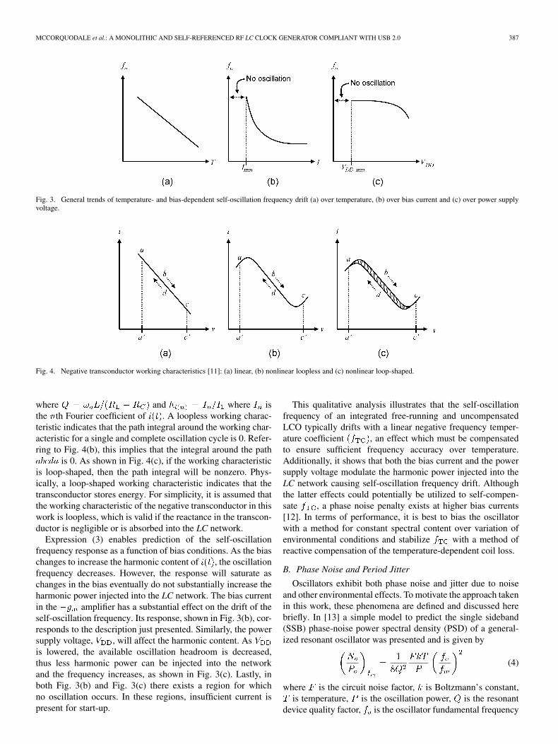
The self-oscillation frequency of an LCO drifts in a pre-dictable manner due to variations in temperature and bias condi-tions, the latter of which includes variations in the power supplyvoltage and bias current. Consider the generalized schematicfor a negative transconductance LCO as shown in Fig. 2.The natural resonant frequency of the LC network is
. Considering the parasitic losses of the coil, ,and of the tank capacitance, , the oscillation frequency must
Fig. 2. Generalized schematic of a �g LCO.
be redetermined by solving for the zero phase of the lossynetwork, which yields
(1)
In most integrated LCOs, the coil loss is substantially largerthan the loss in the equivalent tank capacitance, so (1) can beapproximated by
(2)
For the purpose of predicting the self-oscillation frequencydrift, both and exhibit negligible bias and temperaturecoefficients. The former was shown in [10], and the latter istrue as long as thin-film capacitors are utilized. With as theonly temperature-dependent parameter in (2), integrated LCOsexhibit a substantially linear negative temperature coefficient(TC), as illustrated in Fig. 3(a). To stabilize the TC, a method ofreactive compensation of the temperature-dependent coil lossmust be introduced. Additionally, bias-dependent drift, shownin Fig. 3(b) and Fig. 3(c), must be addressed.
Expressions (1) and (2) are valid only for a amplifierthat exhibits a linear current–voltage working character-istic; a response illustrated in Fig. 4(a). Practical ampli-fiers exhibit nonlinear behavior at the extremes of the voltageexcursions. A treatment of the effects of a nonlinear negativetransconductor working characteristic was presented in [11] andit was shown that an increase in the harmonic content of the cur-rent, , driven into the LC network results in a decrease in theoscillation frequency relative to . Physically, this effect arisesfrom a work imbalance between the inductor and capacitor inthe presence of a driving signal with high harmonic content [11].Because the capacitor presents a substantially lower impedanceat high frequencies, in comparison to the inductor, it absorbsthe majority of the spectral content of . Consequently, theoscillation frequency is reduced to the point at which the workbetween the two balances. Considering this work imbalance,a method of reactive power balance of harmonics can be em-ployed to determine the oscillation frequency [11]. For the LCOshown in Fig. 2, if the working characteristic is loopless,as shown in Fig. 4(b), the oscillation frequency is given by
(3)
MCCORQUODALE et al.: A MONOLITHIC AND SELF-REFERENCED RF LC CLOCK GENERATOR COMPLIANT WITH USB 2.0 387
Fig. 3. General trends of temperature- and bias-dependent self-oscillation frequency drift (a) over temperature, (b) over bias current and (c) over power supplyvoltage.
Fig. 4. Negative transconductor working characteristics [11]: (a) linear, (b) nonlinear loopless and (c) nonlinear loop-shaped.
where and where isthe th Fourier coefficient of . A loopless working charac-teristic indicates that the path integral around the working char-acteristic for a single and complete oscillation cycle is 0. Refer-ring to Fig. 4(b), this implies that the integral around the path
is 0. As shown in Fig. 4(c), if the working characteristicis loop-shaped, then the path integral will be nonzero. Phys-ically, a loop-shaped working characteristic indicates that thetransconductor stores energy. For simplicity, it is assumed thatthe working characteristic of the negative transconductor in thiswork is loopless, which is valid if the reactance in the transcon-ductor is negligible or is absorbed into the LC network.
Expression (3) enables prediction of the self-oscillationfrequency response as a function of bias conditions. As the biaschanges to increase the harmonic content of , the oscillationfrequency decreases. However, the response will saturate aschanges in the bias eventually do not substantially increase theharmonic power injected into the LC network. The bias currentin the amplifier has a substantial effect on the drift of theself-oscillation frequency. Its response, shown in Fig. 3(b), cor-responds to the description just presented. Similarly, the powersupply voltage, , will affect the harmonic content. Asis lowered, the available oscillation headroom is decreased,thus less harmonic power can be injected into the networkand the frequency increases, as shown in Fig. 3(c). Lastly, inboth Fig. 3(b) and Fig. 3(c) there exists a region for whichno oscillation occurs. In these regions, insufficient current ispresent for start-up.
This qualitative analysis illustrates that the self-oscillationfrequency of an integrated free-running and uncompensatedLCO typically drifts with a linear negative frequency temper-ature coefficient , an effect which must be compensatedto ensure sufficient frequency accuracy over temperature.Additionally, it shows that both the bias current and the powersupply voltage modulate the harmonic power injected into theLC network causing self-oscillation frequency drift. Althoughthe latter effects could potentially be utilized to self-compen-sate , a phase noise penalty exists at higher bias currents[12]. In terms of performance, it is best to bias the oscillatorwith a method for constant spectral content over variation ofenvironmental conditions and stabilize with a method ofreactive compensation of the temperature-dependent coil loss.
B. Phase Noise and Period Jitter
Oscillators exhibit both phase noise and jitter due to noiseand other environmental effects. To motivate the approach takenin this work, these phenomena are defined and discussed herebriefly. In [13] a simple model to predict the single sideband(SSB) phase-noise power spectral density (PSD) of a general-ized resonant oscillator was presented and is given by
(4)
where is the circuit noise factor, is Boltzmann’s constant,is temperature, is the oscillation power, is the resonant
device quality factor, is the oscillator fundamental frequency

388 IEEE JOURNAL OF SOLID-STATE CIRCUITS, VOL. 42, NO. 2, FEBRUARY 2007
Fig. 5. (a) Effects of frequency multiplication and division on the phase-noise PSD. (b) Phase-noise PSD for a typical PLL clock synthesizer in relationship tothe period jitter integration mask.
and is the frequency offset from the fundamental. Expression(4) is useful as it models the “white of frequency” or regionof the SSB phase-noise PSD, which is typically the broadest.One of the most important insights obtained from (4) is the in-verse-square relationship between phase noise and , an obser-vation which will be discussed subsequently.
In digital systems, clock jitter metrics are of primary interestin contrast to communication systems where the stability metricof interest is phase noise. Jitter metrics quantify the time domainuncertainty in the oscillation period. The most common metricsfor digital clock generation include period and cycle-to-cyclejitter. Define the ideal oscillation period as , theabsolute instant in time of the th positive voltage transitionof the clock signal as and the period of the th cycle aswhere . Assuming that the phase noise is azero-mean stochastic process, the expected value of the discreterandom sequence is . Period jitter is defined inrelationship to any th and subsequent edge as
(5)
is the standard deviation of a single period, which is equivalentto the root mean square period jitter, , for a large samplesize. Cycle-to-cycle jitter is defined in relationship to adjacentcycles as
(6)
and if each cycle is independent, then by definition it can beshown that .
Typically, the timing budget for the clock signal is determinedwith respect to the peak-to-peak period or cycle-to-cycle jitter.These metrics vary over the observation interval because the dis-tribution of the clock period for a signal exhibiting exclusivelyrandom jitter yields a zero-mean distribution with unbounded
tails. Consequently and for example, peak-to-peak period jitteris determined from by selecting a bounding bit-error
rate (BER) and multiplying by the appropriate scale factor,. A BER used commonly for clock specifications is 10 , in-
dicating that statistically only 1 in 10 edges will exceed .Assuming a zero-mean Gaussian distribution, the scale factor isdetermined by solving for given the BER where
erfc BER where erfc
(7)
For a BER of 10 , 14.069 and for a BER of 10 ,16.444.
C. Frequency Multiplication and Division Effects on PhaseNoise
It has been shown in [14] that linear frequency multiplicationand division results in a quadratic change in phase noise power.If a signal at frequency is multiplied by to a frequency
, then the phase noise power of the signal at is , or20 on a logarithmic scale, greater than the phase noisepower at . Similarly, if the signal is divided in frequency by
, the phase noise power decreases by or 20 . Bothresults are illustrated in Fig. 5(a). Because both frequency multi-plication/division and have quadratic relationships to the SSBphase-noise PSD far-from-carrier, it can be considered that fre-quency multiplication and division effectively degrade and en-hance the of the reference oscillator, respectively, yielding aneffective quality factor at the new frequency [15]. There-fore, it is possible for a low-frequency reference oscillator withvery high ( ) multiplied in frequency by the factor tohave the same or similar SSB phase-noise PSD at the new fre-quency as a high-frequency reference oscillator with a very low

MCCORQUODALE et al.: A MONOLITHIC AND SELF-REFERENCED RF LC CLOCK GENERATOR COMPLIANT WITH USB 2.0 389
( ) divided in frequency by the factor . for eachcase is given by
and (8)
The relationships in (8) ignore the noise contribution of ad-ditional circuit components and, referring to (4), assume that
and are the same for both reference oscillators, though itis trivial and algebraic to account for initial discrepancies inand between two different circuits. Consider the followingquantitative and practical example. Gigahertz clocks in micro-processors are typically derived from reference clocks at ap-proximately 100 MHz. If the XTAL for these reference clocksis 1 MHz and the loaded quality factor is 10 , then to syn-thesize 100 MHz, and by (8), . Nowconsider a 2 GHz LCO with a loaded quality factor of 5. Togenerate 100 MHz, and . This suggeststhat the SSB phase-noise PSD of both clock signals at 100 MHzwould be similar. The analysis presents an opportunity to uti-lize the effects of frequency multiplication and division to ad-dress the issue of substantially differing -factors between LCand XTAL resonators, thus motivating the approach presentedin this work.
D. Frequency Multiplication and Division Effects on PeriodJitter
The effects of frequency multiplication and division on pe-riod jitter can be considered by analyzing the case of frequencydivision. Asynchronous frequency division of a periodic signalcauses the magnitude of the period jitter to increase. A dividercircuit will output one pulse for input pulses, thus the vari-ance of the output period is the sum of the variances of theinput periods due to the statistical independence of the positionof each pulse in time. Because the period jitter is the standarddeviation of the period, the period jitter of a signal divided infrequency by is given by where is the pe-riod jitter before frequency division. A converse argument canbe presented for the case of frequency multiplication which, incontrast, reduces the period jitter by the same factor. This mayseem counterintuitive as the SSB phase-noise PSD is reducedby frequency division. Consider the fact that although the pe-riod jitter has increased by , the period has also increasedby . Therefore, it is instructive to describe the fractional pe-riod jitter in ppm as given by whereis the period and is either or . Thus, the fractionalperiod jitter for a signal divided in frequency by is given by
(9)
which is reduced by frequency division. The fractional periodjitter is increased by the same factor for the case of frequencymultiplication. However, if a divider stage is resynchronized bya flip-flop and a faster clock, then the jitter at the output of thestage will match that of the synchronizing clock signal. Bothasynchronous and synchronous frequency division are utilizedin this work.
E. Period Jitter and the Relationship to Phase Noise
It has been shown in [14] and [16] that the period jitter canbe related to the phase-noise PSD by the following expression:
(10)
where is the oscillation frequency, is the phase-noise PSD at frequency offset from the carrier frequency,
is the transfer function with equivalent cut-off frequencyand . The expression shows that is de-
termined by the integral of the projection of onto atrigonometric function with period , the latter of whichcan be considered as a mask of . Equation (10) showsthat the trigonometric mask reduces the close-to-carrier contri-butions of the phase-noise PSD to the period jitter. As in-creases, the trigonometric mask also increases and the phase-noise PSD contributes more substantially to the period jitter. InRF systems, the close-to-carrier phase noise is often of substan-tial concern as it can cause reciprocal mixing in receivers thatcan mask downconversion of the desired signal [17]. However,when considering the period jitter for digital clock signals, theclose-to-carrier phase noise is less significant. In fact, as shownin (10), the far-from-carrier phase noise contributes more signif-icantly to the period jitter, representing another significant ob-servation to the approach taken in this work.
Consider these observations further and in relationship to atypical XO-referenced PLL clock synthesizer with a dividerratio of . For such a clock synthesizer, the output phase noisepath will track the reference oscillator for offset frequencieswithin the loop bandwidth (BW) of the PLL but shifted by
20 due to frequency multiplication, as shown inFig. 5(b). Outside the loop BW of the PLL, the output phasenoise path will track the VCO, which is typically a ring os-cillator exhibiting relatively high phase noise, as shown inFig. 5(b). Now consider the total output phase noise path inrelationship to the period jitter integration mask. As shown inFig. 5(b), not only does frequency multiplication and divisionaffect the phase-noise PSD and period jitter, but so does thehigh far-from-carrier phase noise due to tracking the ring VCOoutside of the PLL loop BW. In fact, the difference in thefar-from-carrier phase-noise PSD between phase-locked ringoscillators and LCOs can be as high as 50 dB [18]. In compar-ison, a free-running LCO with a high frequency division ratiomay exhibit lower period jitter than an XO-referenced PLLdue to differences in both frequency multiplication/divisionand far-from-carrier phase noise. These observations furthermotivate the approach taken in this work as well as justify thefact that self-referenced and relatively low- RF LC resonatorscan be used to generate very low-jitter clock signals which arelikely to achieve the performance required for a broad range ofapplications. The analysis also illustrates that high- frequencyreferences for ring-PLLs are unlikely to achieve low jitter atthe output, thus nullifying the benefits of a high- frequencyreference.

390 IEEE JOURNAL OF SOLID-STATE CIRCUITS, VOL. 42, NO. 2, FEBRUARY 2007
Fig. 6. USB 2.0 compliant RF-TCHO clock generator architecture.
III. RF-TCHO CLOCK GENERATOR IMPLEMENTATION
A. RF-TCHO Clock Generator Architecture
The architecture of the developed RF-TCHO clock gener-ator macro is shown in Fig. 6, where each functional block isshown in simplified form as a module. The entire macro is pow-ered by a 3.3-V rail which is derived from a 5-V bandgap refer-enced voltage regulator. The LC reference oscillator operates at1.536 GHz, which facilitates frequency division by powers of 2,thus simplifying the divider implementation and reducing thelikelihood of introducing deterministic jitter. A divide-by-2 cur-rent-mode logic (CML) stage buffers the oscillator from the fre-quency divider stages while providing a constant and state-in-dependent load. The next frequency divider is also a CML di-vider which is followed by a CML-to-CMOS converter. Thenext five divider stages are implemented with static D-flip-flopswhich ensure 50/50 duty-cycle. The first two static dividers areasynchronous and the remaining three are synchronous. Fre-quency division by 2 yields 96 MHz for the SoC logic andan additional division by 2 yields 12 MHz for the FS-USB.Clock signals at 48 MHz (serving as a reference for an off-chipHS-USB PHY) and 12 MHz (for the on-chip FS-USB PHY) arethe only clock signals that are driven off-chip. A temperature-and supply-independent current reference, , biases theamplifier and maintains constant harmonic content in the LCnetwork, thus minimizing bias-induced frequency drift. Tem-perature compensation is achieved open-loop with a reactivecompensation method using a programmable array of accumu-lation-mode MOS (A-MOS) varactors that are biased by either atemperature-dependent voltage , or by a temperature-in-dependent voltage , both of which are derived from temper-ature-dependent current sources, and , along withresistors. The uncompensated is expected to be negativedue to the coil loss . Consequently, must increaseover temperature to reduce the net tank capacitance and main-tain the self-oscillation frequency. To account for process vari-ation, programmable discrete frequency calibration was imple-mented as a switched-capacitor array with poly–insulator–poly(PiP) capacitors and nMOS switches, as shown in Fig. 6. The
Fig. 7. 1.536 GHz clock generator �g reference oscillator.
physical design of the nMOS switches employs a ring structure,identical to that used in [19], which minimizes the parasitic de-vice capacitance across the switch.
A schematic of the 1.536 GHz reference oscillatoris shown in Fig. 7. It is a complementary and cross-coupledtopology where the pMOS and nMOS devices are sized suchthat the rise and fall times of the oscillation cycle are nearlyequal, a design objective which is known to reduce the phasenoise [12]. Additionally, transistors were sized to provide suf-ficient transconductance for start-up and to ensure oscillation

MCCORQUODALE et al.: A MONOLITHIC AND SELF-REFERENCED RF LC CLOCK GENERATOR COMPLIANT WITH USB 2.0 391
Fig. 8. Bias circuitry.
over design corners. The oscillator is biased from a 500 Atemperature- and bias-independent reference current thatis scaled by a factor of 11 through a cascoded current mirror,providing 5.5 mA to the amplifier and yielding an overde-sign factor of approximately 5. Transistors and arereset devices used to disable the reference oscillator and placeit into a minimum current standby state.
The bias current generation circuitry is shown in Fig. 8.Both proportional to absolute temperature (PTAT) and com-plementary to absolute temperature (CTAT) current referencesare generated. The former is derived from a -referencedself-biased topology that includes nMOS devices in weakinversion. The latter is derived from a standard -referencedself-biased topology. Both reference circuits contain start-upcircuitry and reset transistors, the latter of which are requiredto place the bias generators in a minimum current standbystate. From these current references, the temperature- andbias-independent reference current is derived by sum-ming appropriate weights of the PTAT and CTAT references,providing constant spectral content operation in theamplifier. and are used to generate and
, respectively.
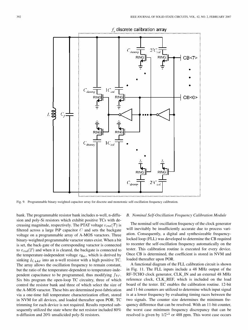
Fig. 9 illustrates the programmable binary-weighted PiP ca-pacitor array for discrete and monotonic frequency calibration.Eight calibration bits were implemented, enabling a 2.56%frequency calibration range with 200 ppm increments, yielding
100 ppm as the worst case initial frequency inaccuracy. TheMSB switches 1.2 pF and the LSB switches 25 fF into the tank.As shown in Fig. 9, dummy capacitor structures, which wereconstructed of minimum size PiP capacitors with a nominalcapacitance of 10 fF, were required because it was determinedthat differences in the number of active switches withoutdummies modified slightly. The dummy structures ensurethat the same number of switches are active for all calibrationstates and that the difference between any two states constitutesdifferences in the net capacitance exclusively. The calibrationbyte (CB) is determined post-fabrication with a module that isdescribed in the next section. Once determined, CB is storedin one-time-programmable (OTP) nonvolatile memory (NVM)and then loaded thereafter upon power-on reset (POR).
The open-loop reactive temperature compensation circuitryis shown in Fig. 10. The PTAT current is driven into oneof three selectable resistor banks, all of the same magnitude,but of differing TCs depending on the type of resistors in the
392 IEEE JOURNAL OF SOLID-STATE CIRCUITS, VOL. 42, NO. 2, FEBRUARY 2007
Fig. 9. Programmable binary-weighted capacitor array for discrete and monotonic self-oscillation frequency calibration.
bank. The programmable resistor bank includes n-well, n-diffu-sion and poly-Si resistors which exhibit positive TCs with de-creasing magnitude, respectively. The PTAT voltage isfiltered across a large PiP capacitor and sets the backgatevoltage on a programmable array of A-MOS varactors. Threebinary-weighted programmable varactor states exist. When a bitis set, the back-gate of the corresponding varactor is connectedto and when it is cleared, the backgate is connected tothe temperature-independent voltage , which is derived bysinking into an n-well resistor with a high positive TC.The array allows the oscillation frequency to remain constant,but the ratio of the temperature-dependent to temperature-inde-pendent capacitance to be programmed, thus modifying .Six bits program the open-loop TC circuitry, three of whichcontrol the resistor bank and three of which select the size ofthe A-MOS varactor. These bits are determined post-fabricationvia a one-time full temperature characterization effort, storedin NVM for all devices, and loaded thereafter upon POR. TCtrimming for each device is not required. Results reported sub-sequently utilized the state where the net resistor included 80%n-diffusion and 20% unsalicided poly-Si resistors.
B. Nominal Self-Oscillation Frequency Calibration Module
The nominal self-oscillation frequency of the clock generatorwill inevitably be insufficiently accurate due to process vari-ation. Consequently, a digital and synthesizeable frequency-locked loop (FLL) was developed to determine the CB requiredto recenter the self-oscillation frequency automatically on thetester. This calibration routine is executed for every device.Once CB is determined, the coefficient is stored in NVM andloaded thereafter upon POR.
A functional diagram of the FLL calibration circuit is shownin Fig. 11. The FLL inputs include a 48 MHz output of theRF-TCHO clock generator, CLK_IN and an external 48 MHzreference clock, CLK_REF, which is included on the loadboard of the tester. EC enables the calibration routine. 12-bitand 11-bit counters are utilized to determine which input signalis at a lower frequency by evaluating timing races between thetwo signals. The counter size determines the minimum fre-quency difference that can be resolved. With an 11-bit counter,the worst case minimum frequency discrepancy that can beresolved is given by 1/2 or 488 ppm. This worst case occurs

MCCORQUODALE et al.: A MONOLITHIC AND SELF-REFERENCED RF LC CLOCK GENERATOR COMPLIANT WITH USB 2.0 393
Fig. 10. Programmable open-loop temperature compensation circuitry including a binary-weighted varactor array, a programmable temperature-dependent controlvoltage and a temperature-independent voltage.
only when the frequencies of the two signals are very close,the faster clock edge occurs immediately before the calibrationroutine is initiated, and the slower clock edge occurs imme-diately after it is initiated. In such a case, it will take all 2cycles for the phases of the two signals to drift past each otherbefore the minimum frequency discrepancy can be resolved.Away from this boundary condition, much finer tolerancecan be resolved. Nevertheless, to ensure convergence to theoptimal state, five calibration routines are run per device andthe statistical mode of the results is selected. The results of thetiming races are determined by the time order of the transitionsof the MSB of the reference clock counter (REF_MSB) andthe terminal count of the RF-TCHO clock counter (CLK_TC).These signals drive an up/down counter and state machine thatdetermines whether to increase or decrease the frequency of theRF-TCHO clock by decrementing or incrementing the currentCB value respectively. The calibration module can be bypassedand data can be written directly into the CB register either fromNVM or externally.
Fig. 12 illustrates the state diagram for the calibrationmodule. The default state is IDLE. Once calibration is enabled
by setting EC , the calibration routine is initiated. Theroutine stalls until the REF_MSB is set before beginning totrack the counters, a technique which provides stabilizationtime between the last CB change and the next race. Once a racebegins, if the RF-TCHO clock counter reaches its highest state(CLK_TC ) and REF_MSB has not been reset, then theRF-TCHO clock is faster and CB is incremented to add morecapacitance into the LC network and reduce the frequency.Conversely, if REF_MSB is reset and CLK_TC is still low,then the reference clock is faster and CB is decremented. Whenboth conditions occur, the routine completes. Two flip-flops, asshown in Fig. 12, form the synchronization boundary betweenthe two asynchronous clock domains. One flip-flop synchro-nizes REF_MSB with CLK_IN. The resulting signal, SYNC,has known timing with respect to CLK_IN which is used toclock the state machine. The other flip-flop is used to generate asynchronized signal for initializing the reference clock counterproperly. The reference clock counter is initialized when thestate machine is in states other than START or TRACK. TheRF-TCHO clock counter is initialized when the state machineis in states other than TRACK. Each increment or decrement

394 IEEE JOURNAL OF SOLID-STATE CIRCUITS, VOL. 42, NO. 2, FEBRUARY 2007
Fig. 11. Functional diagram of digital and synthesizable frequency-locked loop (FLL) calibration module.
Fig. 12. State diagram and synchronization logic for the FLL calibration module.
requires up to 2 cycles of the 48 MHz reference clock or ap-proximately 42.7 s. At most, 128 changes to CB are required,yielding a maximum calibration latency of 5.47 ms per routine.Thus, the maximum calibration latency for each device is27.35 ms because five routines are executed per device. Typicalmeasured calibration latency was less than 10 ms.
IV. MEASUREMENT RESULTS
A micrograph of the RF-TCHO clock generator macro, whichoccupies 0.22 mm in a dual-gate (DG) two-poly four-metal(2P4M) 0.35 m CMOS process, is shown in Fig. 13. Thecalibration FLL is not shown as it was synthesized with the

MCCORQUODALE et al.: A MONOLITHIC AND SELF-REFERENCED RF LC CLOCK GENERATOR COMPLIANT WITH USB 2.0 395
Fig. 13. Macro micrograph of RF-TCHO clock generator in a 0.35 �m 2P4MDG CMOS process.
remainder of the logic in the SoC. The DG option was requiredto support 5-V I/O and power for the USB, while the secondpoly-Si layer was required to realize the PiP capacitors. A 4-nHspiral hollow-core inductor was realized by interconnectingmetal-3 and metal-4 in parallel, a topology which is known toprovide a high -factor for planar inductors [20]. The estimatedloaded -factor for this structure is 5, resulting, per (8), in a
of 640 for the 12 MHz clock due to frequency divisionby a factor of 128. The clock generator draws 9.5 mA from theregulated 3.3-V power supply. Although the current is high fora low frequency clock generator, it is acceptable consideringthat for the given application power is provided via the PCUSB port and an off-chip discrete XO that dissipated a similaramount of power was replaced in this application. Nevertheless,a trade-off between and power does exist. However, in futurerevisions of the device, the power dissipation can be reduced aswill be discussed.
The SoC into which the clock generator was embedded in-cludes an FS-USB PHY interface. Thus, the macro can be con-trolled and programmed completely by any PC that supportsUSB 2.0. The SoC was packaged in a plastic SSOP and assem-bled onto a PCB for environmental test. First, the nominal fre-quency of each device was calibrated post-fabrication with theembedded calibration FLL described previously and an external48 MHz crystal clock reference which was included on the loadboard for the tester. Once the correct CB was determined, it
Fig. 14. Time-domain waveform of calibrated 12 MHz clock at roomtemperature.
was written into NVM. A sample time-domain waveform ofthe post-calibration clock signal is shown in Fig. 14 where theself-oscillation frequency is 11.9991 MHz.
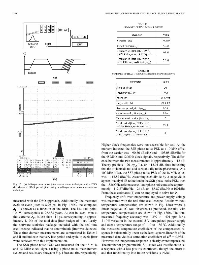
The nominal period jitter was measured with two techniques.First, a 12.5 GSa/s digital sampling oscilloscope (DSO) anda self-synchronization technique were used as illustrated inFig. 15(a) and described in [21]. Jitter was measured using theinfinite persistence mode of the DSO to collect approximately20k samples of the first positive clock edge that occurredafter the trigger edge, where the trigger was set at 50% of thesignal amplitude for a rising edge. The delay element shown inFig. 15(a) was not required because the period of the 12 MHzclock signal is larger than the internal delay of the instrument.Ignoring the embedded trigger jitter, the measured jitter of thefirst edge following the trigger event was 4.732 ps as shownin Fig. 15(b), corresponding to 66.57 ps assuming a BERof 10 .
Although this measurement approach represents a standardtechnique by which the can be determined, it is subjectto errors due to variation in the test set-up including the load,trigger threshold and trigger jitter. Consequently, a 20 GSa/sreal-time oscilloscope was utilized to capture 30 kSa of theoscillation period, from which statistics could be computed.This approach differs substantially from the former as the datacaptured are a collection of subsequent period measurementsover time, thus enabling cycle-to-cycle jitter measurements.Fig. 16(a) shows the distribution of the period measurementswhich appears Gaussian centered around 83.33958 ns with astandard deviation of 6.78 ps, which is slightly higher than
396 IEEE JOURNAL OF SOLID-STATE CIRCUITS, VOL. 42, NO. 2, FEBRUARY 2007
Fig. 15. (a) Self-synchronization jitter measurement technique with a DSO.(b) Measured RMS period jitter using a self-synchronization measurementtechnique.
measured with the DSO approach. Additionally, the measuredcycle-to-cycle jitter is 8.96 ps. In Fig. 16(b), the computed
is shown as a function of the BER. The last data point,10 , corresponds to 26.438 years. As can be seen, even atthis extreme, is less than 111 ps, corresponding to approx-imately 1/10th of the total data jitter budget of 1 ns. Lastly,the software statistics package included with the real-timeoscilloscope indicated that no deterministic jitter was detected.These time-domain measurements are summarized in Tables Iand II and indicate that very low period and cycle-to-cycle jitterwere achieved with this implementation.
The SSB phase-noise PSD was measured for the 48 MHzand 12 MHz clock signals using a phase noise measurementsystem and results are shown in Fig. 17(a) and (b), respectively.
TABLE ISUMMARY OF DSO MEASUREMENTS
TABLE IISUMMARY OF REAL-TIME OSCILLOSCOPE MEASUREMENTS
Higher clock frequencies were not accessible for test. As themarkers indicate, the SSB phase-noise PSD at a 10 kHz offsetfrom the carrier was 90.86 dBc/Hz and 103.08 dBc/Hz forthe 48 MHz and 12 MHz clock signals, respectively. The differ-ence between the two measurements is approximately 12 dB.Theory predicts 20 , or 12.04 dB, thus indicatingthat the dividers do not add substantially to the phase noise. At a100 kHz offset, the SSB phase-noise PSD of the 48 MHz clockwas 112.87 dBc/Hz. Assuming each divide-by-2 stage yieldsapproximately 6 dB reduction in the SSB phase-noise PSD, thenthe 1.536 GHz reference oscillator phase noise must be approxi-mately 112.87 dBc/Hz 24 dB, or 88.87 dBc/Hz at 100 kHz.From these estimates (4) can be employed to solve for .
Frequency drift over temperature and power supply voltagewas measured with the real-time oscilloscope. Results withouttemperature compensation are shown in Fig. 18(a) where alinear negative TC was observed as predicted. Results withtemperature compensation are shown in Fig. 18(b). The totalmeasured frequency accuracy was 397 to 401 ppm for a
10% variation in the external 5-V unregulated power supplyand over a temperature range of 10 to 85 C. Additionally,the measured temperature coefficient of the compensated re-sponse is substantially linear as the least-squares linear fit of themeasured data yields a correlation coefficient of 0.9351.However, the temperature response is clearly overcompensated.The number of programmable states was insufficient to seta response with a less positive coefficient, though the effort toadd that functionality into future revisions is trivial.

MCCORQUODALE et al.: A MONOLITHIC AND SELF-REFERENCED RF LC CLOCK GENERATOR COMPLIANT WITH USB 2.0 397
Fig. 16. Real-time oscilloscope measurements. (a) Jitter histograms and statistics. (b) � jitter versus BER.
Fig. 17. Measured SSB phase-noise PSD of the clock generator. (a) 48 MHz.(b) 12 MHz.
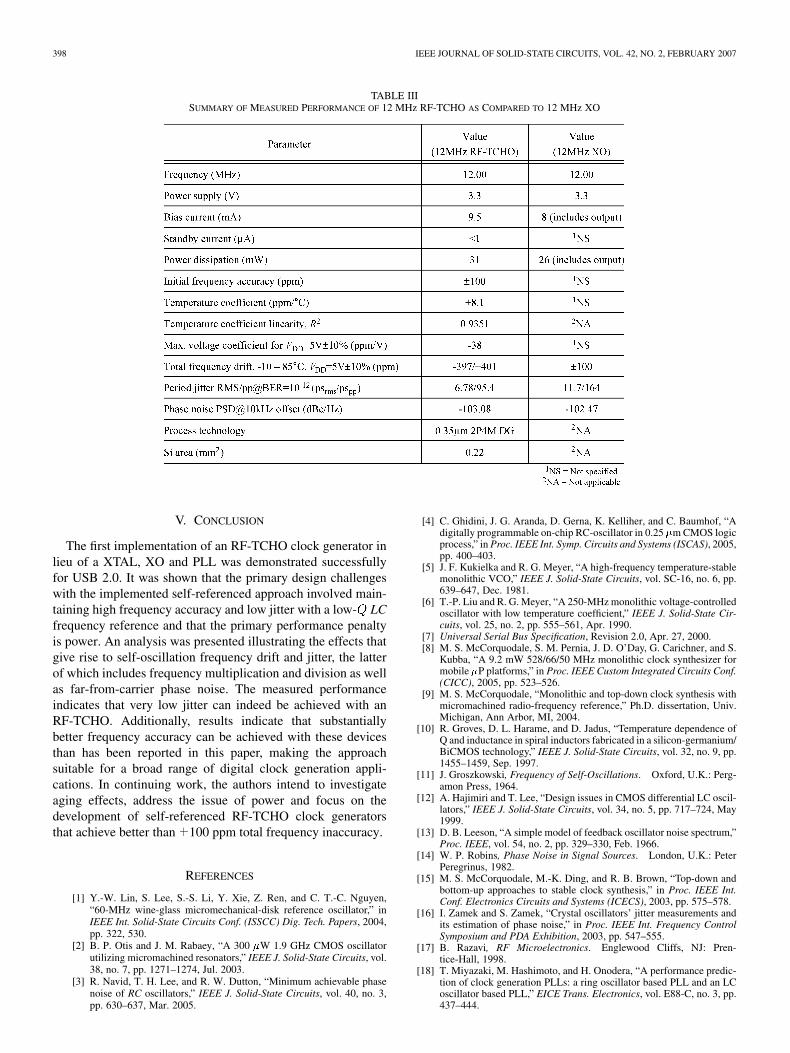
For comparative purposes, period jitter and phase noise mea-surements were performed on a standard commercial 12 MHzXO using identical measurement techniques. The measuredperformance is summarized in Table III and compared to theperformance achieved with the RF-TCHO. Both approachesachieve compliance with the specification for USB 2.0, butthe RF-TCHO design does not require a XTAL. However, thepower dissipation is higher with the RF-TCHO. Though theXO output driver is included in the total power measurement,it is worth noting that the load was 4 pF and high impedance,thus output current draw was small. Power can be addressedin the RF-TCHO by minimizing the overdesign in the LCOand reducing the power in the CML divider stages. By addingadditional programmable temperature compensation states it
Fig. 18. Normalized frequency accuracy (a) without f compensation versustemperature for V = 5V (b) with f compensation versus temperature forV = 5 V � 10%.
is quite likely that the total frequency drift can be decreasedsignificantly, thus making the demonstrated approach directlycompetitive with XO-referenced and phase-locked digital clocksynthesizers. In particular, results indicate that the clock fre-quency accuracy required for other bus protocols such as PCI( 300 ppm) or IEEE1394 ( 100 ppm) may be achievable.
398 IEEE JOURNAL OF SOLID-STATE CIRCUITS, VOL. 42, NO. 2, FEBRUARY 2007
TABLE IIISUMMARY OF MEASURED PERFORMANCE OF 12 MHz RF-TCHO AS COMPARED TO 12 MHz XO
V. CONCLUSION
The first implementation of an RF-TCHO clock generator inlieu of a XTAL, XO and PLL was demonstrated successfullyfor USB 2.0. It was shown that the primary design challengeswith the implemented self-referenced approach involved main-taining high frequency accuracy and low jitter with a low- LCfrequency reference and that the primary performance penaltyis power. An analysis was presented illustrating the effects thatgive rise to self-oscillation frequency drift and jitter, the latterof which includes frequency multiplication and division as wellas far-from-carrier phase noise. The measured performanceindicates that very low jitter can indeed be achieved with anRF-TCHO. Additionally, results indicate that substantiallybetter frequency accuracy can be achieved with these devicesthan has been reported in this paper, making the approachsuitable for a broad range of digital clock generation appli-cations. In continuing work, the authors intend to investigateaging effects, address the issue of power and focus on thedevelopment of self-referenced RF-TCHO clock generatorsthat achieve better than 100 ppm total frequency inaccuracy.
REFERENCES
[1] Y.-W. Lin, S. Lee, S.-S. Li, Y. Xie, Z. Ren, and C. T.-C. Nguyen,“60-MHz wine-glass micromechanical-disk reference oscillator,” inIEEE Int. Solid-State Circuits Conf. (ISSCC) Dig. Tech. Papers, 2004,pp. 322, 530.
[2] B. P. Otis and J. M. Rabaey, “A 300 �W 1.9 GHz CMOS oscillatorutilizing micromachined resonators,” IEEE J. Solid-State Circuits, vol.38, no. 7, pp. 1271–1274, Jul. 2003.
[3] R. Navid, T. H. Lee, and R. W. Dutton, “Minimum achievable phasenoise of RC oscillators,” IEEE J. Solid-State Circuits, vol. 40, no. 3,pp. 630–637, Mar. 2005.
[4] C. Ghidini, J. G. Aranda, D. Gerna, K. Kelliher, and C. Baumhof, “Adigitally programmable on-chip RC-oscillator in 0.25 �m CMOS logicprocess,” in Proc. IEEE Int. Symp. Circuits and Systems (ISCAS), 2005,pp. 400–403.
[5] J. F. Kukielka and R. G. Meyer, “A high-frequency temperature-stablemonolithic VCO,” IEEE J. Solid-State Circuits, vol. SC-16, no. 6, pp.639–647, Dec. 1981.
[6] T.-P. Liu and R. G. Meyer, “A 250-MHz monolithic voltage-controlledoscillator with low temperature coefficient,” IEEE J. Solid-State Cir-cuits, vol. 25, no. 2, pp. 555–561, Apr. 1990.
[7] Universal Serial Bus Specification, Revision 2.0, Apr. 27, 2000.[8] M. S. McCorquodale, S. M. Pernia, J. D. O’Day, G. Carichner, and S.
Kubba, “A 9.2 mW 528/66/50 MHz monolithic clock synthesizer formobile �P platforms,” in Proc. IEEE Custom Integrated Circuits Conf.(CICC), 2005, pp. 523–526.
[9] M. S. McCorquodale, “Monolithic and top-down clock synthesis withmicromachined radio-frequency reference,” Ph.D. dissertation, Univ.Michigan, Ann Arbor, MI, 2004.
[10] R. Groves, D. L. Harame, and D. Jadus, “Temperature dependence ofQ and inductance in spiral inductors fabricated in a silicon-germanium/BiCMOS technology,” IEEE J. Solid-State Circuits, vol. 32, no. 9, pp.1455–1459, Sep. 1997.
[11] J. Groszkowski, Frequency of Self-Oscillations. Oxford, U.K.: Perg-amon Press, 1964.
[12] A. Hajimiri and T. Lee, “Design issues in CMOS differential LC oscil-lators,” IEEE J. Solid-State Circuits, vol. 34, no. 5, pp. 717–724, May1999.
[13] D. B. Leeson, “A simple model of feedback oscillator noise spectrum,”Proc. IEEE, vol. 54, no. 2, pp. 329–330, Feb. 1966.
[14] W. P. Robins, Phase Noise in Signal Sources. London, U.K.: PeterPeregrinus, 1982.
[15] M. S. McCorquodale, M.-K. Ding, and R. B. Brown, “Top-down andbottom-up approaches to stable clock synthesis,” in Proc. IEEE Int.Conf. Electronics Circuits and Systems (ICECS), 2003, pp. 575–578.
[16] I. Zamek and S. Zamek, “Crystal oscillators’ jitter measurements andits estimation of phase noise,” in Proc. IEEE Int. Frequency ControlSymposium and PDA Exhibition, 2003, pp. 547–555.
[17] B. Razavi, RF Microelectronics. Englewood Cliffs, NJ: Pren-tice-Hall, 1998.
[18] T. Miyazaki, M. Hashimoto, and H. Onodera, “A performance predic-tion of clock generation PLLs: a ring oscillator based PLL and an LCoscillator based PLL,” EICE Trans. Electronics, vol. E88-C, no. 3, pp.437–444.

MCCORQUODALE et al.: A MONOLITHIC AND SELF-REFERENCED RF LC CLOCK GENERATOR COMPLIANT WITH USB 2.0 399
[19] A. Kral, F. Behbahani, and A. A. Abidi, “RF-CMOS oscillators withswitched tuning,” in Proc. IEEE Custom Integrated Circuits Conf.(CICC), 1998, pp. 555–558.
[20] J. Craninckx and M. Steyaert, “A 1.8-GHz CMOS low-phase-noisevoltage-controlled oscillator using optimized hollow spiral inductors,”IEEE J. Solid-State Circuits, vol. 32, no. 5, pp. 736–744, May 1997.
[21] M. Shimanouchi, “An approach to consistent jitter modeling for var-ious jitter aspects and methods,” in Proc. IEEE Int. Test Conf. (ITC),2001, pp. 848–857.
Michael S. McCorquodale (S’95–M’04) wasborn in Richardson, TX, on November 12, 1974. Hereceived the B.S.E. degree with honors in electricalengineering from the University of Illinois at Urbana-Champaign in 1997. For the next year, he waswith Hughes Space and Communications Co., ElSegundo, CA, where he developed GHz InP andSiGe digital integrated circuits. In 1998, he begangraduate work at the University of Michigan wherehe completed the M.S.E and Ph.D. degrees in elec-trical engineering in 2000 and 2004, respectively, in
the National Science Foundation’s Engineering Research Center in WirelessIntegrated Microsystems. While at Michigan, he was the sole national recipientof the Armed Forces Communications and Electronics Association (AFCEA)Doctoral Fellowship in 2002. Dr. McCorquodale also received the University ofMichigan College of Engineering Harry B. Benford Entrepreneurial LeadershipAward and the Distinguished University of Michigan Electrical EngineerAward.
He is the founder and Chief Technical Officer of Mobius Microsystems, Inc.,a venture-backed start-up with headquarters in Sunnyvale, CA, and a designcenter in Detroit, MI, and which was founded based on his dissertation work inmonolithic RF LC clock generators.
Justin D. O’Day received the B.S.E. and M.S.E. de-grees in electrical engineering from the Universityof Illinois at Urbana-Champaign in 1998 and 2000,respectively. His graduate research focused on mod-eling and simulation of plasma discharges.
For the next three years, he was with Cadence De-sign Systems VCAD group in Munich, Germany, asan analog and mixed-signal IC design specialist. In2004, he joined Mobius Microsystems, Inc., as itsfirst employee. Currently, he is the Director of De-sign Engineering of Mobius Microsystems’ Design
Center, Detroit, MI.
Scott M. Pernia (M’05) was born in 1979. Hereceived the B.S.E. degree with highest honorsand the M.S.E. degree in electrical engineeringfrom the University of Michigan in 2002 and 2003,respectively. While an undergraduate and a graduatestudent at the University of Michigan, he conductedresearch on low-power pipelined and successiveapproximation register ADCs.
In 2003, he joined Motorola, Inc., FarmingtonHills, MI, as a Senior Analog Design Engineer wherehe worked on solenoid and motor control ASICs for
automotive powertrain. Since 2004, he has been with Mobius Microsystems,Inc., Detroit, MI, working on the development and commercialization ofmonolithic RF LC clock generators.
Mr. Pernia is a member of the Tau Beta Pi Engineering Honor Society andthe Golden Key National Honor Society.
Gordon A. Carichner (M’95) received the B.S.E.and M.S.E. degrees in electrical engineering fromthe University of Michigan in 1989 and 1991,respectively.
He joined Motorola, Inc., Austin, TX, in 1991, de-signing circuits for 16-bit digital signal processors.He returned to the University of Michigan in 1998to teach VLSI design and to support EDA software.In 2004, he joined Mobius Microsystems, Inc., De-troit, MI, where he designs digital and analog circuitsfor monolithic RF LC clock generators. He holds one
U.S. patent with several pending.
Sundus Kubba was born in 1977. She received theB.S.E. and M.S.E. degrees in electrical engineeringfrom Carleton University, Ottawa, Canada, in 1999and 2002, respectively. Her graduate research wasfocused on the design of fully-integrated RF CMOSquadrature voltage-controlled oscillators.
In 2001, she joined Asahi Glass AutomotiveResearch Center, Ypsilanti, MI, where she workedon developing antennas for Satellite Digital AudioRadio Systems (SDARS) applications. She hasbeen with Mobius Microsystems, Inc., Detroit, MI,
since 2005 and has been working on the design of monolithic RF LC clockgenerators.
Richard B. Brown (S’74–M’76–SM’91) receivedthe B.S.E. and M.S.E. degrees in electrical engi-neering from Brigham Young University, Provo,UT, in 1976, and the Ph.D. degree in electricalengineering from the University of Utah, Salt LakeCity, UT, in 1985.
From 1976 to 1981, he worked in computerdesign as Vice-President of Engineering at HolmanIndustries, Oakdale, CA, and then as Manager ofComputer Development at Cardinal Industries, WebbCity, MO. He joined the faculty of the Department
of Electrical Engineering and Computer Science, University of Michigan, in1985, where he served as Associate Chair and Interim Chair. He became theDean of Engineering at the University of Utah in 2004. He has conducted majorresearch projects in the areas of solid-state sensors, mixed-signal circuits,GaAs and silicon-on-insulator circuits, and high-performance and low-powermicroprocessors.
Prof. Brown serves as chairman of the MOSIS Advisory Council for Edu-cation. He was Chair of the 1997 Conference on Advanced Research in VLSIand the 2001 Microelectronic System Education Conference. He has served asGuest Editor of the IEEE JOURNAL OF SOLID-STATE CIRCUITS and PROCEEDINGS
OF THE IEEE and as associate editor of IEEE TRANSACTIONS ON VERY LARGE
SCALE INTEGRATED (VLSI) SYSTEMS.