Embed Size (px)
Citation preview

IEEE JOURNAL OF SOLID-STATE CIRCUITS, VOL. 41, NO. 12, DECEMBER 2006 2885
A 10-Gb/s 5-Tap DFE/4-Tap FFE Transceiver in90-nm CMOS Technology
John F. Bulzacchelli, Member, IEEE, Mounir Meghelli, Sergey V. Rylov, Member, IEEE,Woogeun Rhee, Member, IEEE, Alexander V. Rylyakov, Herschel A. Ainspan, Benjamin D. Parker,
Michael P. Beakes, Member, IEEE, Aichin Chung, Troy J. Beukema, Petar K. Pepeljugoski, Senior Member, IEEE,Lei Shan, Member, IEEE, Young H. Kwark, Member, IEEE, Sudhir Gowda, Member, IEEE, and
Daniel J. Friedman, Member, IEEE
Abstract—This paper presents a 90-nm CMOS 10-Gb/s trans-ceiver for chip-to-chip communications. To mitigate the effectsof channel loss and other impairments, a 5-tap decision feed-back equalizer (DFE) is included in the receiver and a 4-tapbaud-spaced feed-forward equalizer (FFE) in the transmitter.This combination of DFE and FFE permits error-free NRZ sig-naling over channels with losses exceeding 30 dB. Low jitter clocksfor the transmitter and receiver are supplied by a PLL with LCVCO. Operation at 10-Gb/s with good power efficiency is achievedby using half-rate architectures in both transmitter and receiver.With the transmitter producing an output signal of 1200 mVppd,one transmitter/receiver pair and one PLL consume 300 mW.Design enhancements of a half-rate DFE employing one tap ofspeculative feedback and four taps of dynamic feedback allowits loop timing requirements to be met. Serial link experimentswith a variety of test channels demonstrate the effectiveness of theFFE/DFE equalization.
Index Terms—Adaptive equalizer, decision-feedback equalizer,feed-forward equalizer, serial link, transceiver.
I. INTRODUCTION
THE CONTINUING growth in processing power of dig-ital computing engines and the increasing demand for ad-
vanced network services are creating a need for higher band-width data transmission in systems such as servers and datacommunication routers. To meet this need, industry standards[1] are being developed which define the channel characteristicsand I/O electrical specifications of short reach ( 4-in, on-board)and long reach ( 30-in+, intercard) serial links operating atdata rates in excess of 10 Gb/s. While serial link transceivers inthe 6-Gb/s range [2]–[4] are often intended to extend the band-width of “legacy” backplane channels, reliable operation above10 Gb/s will require in many cases improved channel charac-teristics, so the standards above 10 Gb/s are primarily aimed atnew (“greenfield”) backplane designs benefiting from improve-ments in board, connector, and chip-level package technologies.
Even with greenfield backplane designs, however, the need toremain price-competitive will discourage adoption of the mostexotic (and expensive) board, connector, and package technolo-gies. As in the recent past, advanced equalization capabilities in
Manuscript received June 10, 2006; revised August 23, 2006. This workwas supported in part by MPO (Maryland Procurement Office) under ContractH98230-04-C-0920.
The authors are with the IBM Research Division, T. J. Watson ResearchCenter, Yorktown Heights, NY 10598 USA (e-mail: [email protected]).
Digital Object Identifier 10.1109/JSSC.2006.884342
the I/O circuitry will be employed to compensate for the signaldistortions of lower cost interconnect technologies. Optimizingcost tradeoffs at the system level requires knowledge of howmuch equalization is needed for a specific combination of board,connector, and package technologies.
In order to gain a more detailed understanding of these trade-offs between interconnect and circuit technologies, a prototypeof a complete 10-Gb/s serial link has been designed, fabricated,and tested. The project can be divided into two major efforts.One was the development of advanced packaging and boardtechnologies, the design, modeling, and measurements of whichare detailed in [5]. The other was the development of a 90-nmCMOS 10-Gb/s transceiver with 4-tap feed-forward equalizer(FFE) and 5-tap decision-feedback equalizer (DFE), which isthe main topic of this paper. This transceiver has equalizationcapabilities similar to those of the current generation of serial-izer/deserializer (SerDes) ASIC I/O core [2], which operates at6.4 Gb/s.
Section II provides a review of the backplane channel appli-cation and a discussion of the considerations made in definingthe signaling and equalization capabilities of the 10-Gb/s trans-ceiver. Section III describes architectural and circuit details ofthe transceiver components. Section IV discusses the features ofthe link demonstrator test chip and presents the results of sev-eral serial link experiments. A summary in Section V concludesthe paper.
II. BACKGROUND
A. Backplane Channel Characteristics
A typical backplane/line card application is shown inFig. 1(a). A long (30-in or more) transmission line on the back-plane is used to transfer data from a processor or ASIC on oneline card to a processor or ASIC on another line card. Severalphysical effects degrade signal integrity at data rates above afew gigabits per second. Skin effect and dielectric losses of thetransmission lines become severe at these data rates. Via stubson the circuit boards and other impedance discontinuities asso-ciated with the chip packages and connectors cause reflectionseasily observed in the channel impulse response [Fig. 1(b)]. Inthe frequency domain, these reflections cause notches whichfurther degrade the channel frequency response [Fig. 1(c)].Since the transmitted signal is attenuated by loss, it is easilycorrupted by crosstalk from other channels. Even for greenfieldbackplanes with improved board technology, the loss at 5 GHz
0018-9200/$20.00 © 2006 IEEE

2886 IEEE JOURNAL OF SOLID-STATE CIRCUITS, VOL. 41, NO. 12, DECEMBER 2006
Fig. 1. Backplane channel characteristics. (a) Backplane/line card application. (b) Channel impulse response. (c) Channel frequency response.
(Nyquist frequency for 10-Gb/s data) may be 20–30 dB. Withthe channel adding so much loss and distortion to the signal,the data eye at the far end of the link [Fig. 1(a)] is completelyclosed, and advanced equalization is required to recover thetransmitted bits.
B. Signaling and Equalization Considerations
One approach to increasing data rates in high-loss channelsis the use of multilevel signaling such as four-level pulseamplitude modulation (PAM-4) [6]–[8]. Compared to binarynon-return-to-zero (NRZ) signaling at the same data rate,PAM-4 signaling reduces the baud rate (and therefore therequired bandwidth) by a factor of two. On the downside, theadditional voltage levels used in PAM-4 signaling decrease thelevel spacing (vertical eye height) by a factor of three (9.5 dB).These last two statements lead to the following rule of thumb[6]: if the loss difference between NRZ and PAM-4 Nyquistfrequencies exceeds 10 dB, the SNR improvement due to baudrate reduction may exceed the 9.5-dB level spacing penalty,and PAM-4 signaling is likely to give better link performance.Adding a linear equalizer to flatten the channel response doesnot alter this basic analysis, as such a linear equalizer amplifiescrosstalk and other high-frequency noises as much as thedesired signal, leaving the high-frequency SNR unchanged.
On the other hand, adding a nonlinear equalizer in the formof a receive-side DFE does alter the analysis because the DFEis able to flatten the channel response without amplifying noiseor crosstalk. A simple counter-example shows that the conven-tional rule of thumb is invalidated by the use of a DFE. Considertransmitting 12.5-Gb/s data over a channel with the impulse andfrequency responses of a 25th-order Bessel filter, as plotted in
Fig. 2. The cutoff frequency of the Bessel filter has been chosenso that the loss (36.5 dB) at 6.25 GHz is 28 dB greater thanthe loss (8.4 dB) at 3.125 GHz. According to the usual rule ofthumb, this should be a clear-cut case for using PAM-4 overNRZ signaling. To test this assertion, the equalized eye diagramsfor NRZ and PAM-4 signaling over this channel were calculatedwith the high-level link simulation tool described in [2]. Fig. 3shows the results when the receiver includes a 2-tap DFE (inboth NRZ and PAM-4 modes), with no other equalization (suchas FFE) applied. In each of these diagrams, the DFE feedbacksignals are held at constant values across a two baud interval inorder to allow clear inspection of the eye margins for the symbolbeing detected at ps. (Since the DFE feedback signals areonly correct for this symbol, the equalized eye diagrams repre-sented in this fashion are not periodic.) Because of the shortduration of the Bessel filter impulse response, increasing thenumber of DFE taps improves the eye diagrams negligibly. Inthe simulations, the receiver gain is set to unity so the heightsof the vertical eye openings represent the voltage margins forsampling the data, referred back to the receiver input pin. Thesimulated NRZ eye is bigger than the PAM-4 eye both vertically(by 93%) and horizontally (by 20%).
An examination of how post-cursor cancellation by the DFEalters the frequency response of the channel reveals why theusual rule of thumb breaks down here. As shown in Fig. 4(a),the pulse response of the Bessel filter channel has only two sig-nificant pre-cursors and two significant post-cursors when sam-pled at 12.5 GHz. The pre-cursors, main cursor, and post-cur-sors can be treated as a discrete-time sequence [Fig. 4(b)]. Sincethe latch of the receiver only samples its input at discrete times,this discrete-time sequence fully characterizes the channel in

BULZACCHELLI et al.: A 10-Gb/s 5-TAP DFE/4-TAP FFE TRANSCEIVER IN 90-nm CMOS TECHNOLOGY 2887
Fig. 2. Impulse and frequency responses of Bessel filter channel.
Fig. 3. Simulated PAM-4 and NRZ eye diagrams for Bessel filter channel.
terms of its effect on the signal being detected. Taking a dis-crete-time Fourier transform (DFT) of this sequence yields theunequalized frequency response of the channel. Assuming thatthe DFE has enough taps and is accurately adapted, the DFEfeedback cancels out the post-cursors of this discrete-time se-quence. Therefore, the frequency response of the serial link afterapplying the DFE can be obtained by taking a DFT of the se-quence comprising only the pre-cursors and main cursor. Ap-plying this method to the Bessel filter example yields the fre-quency responses shown in Fig. 4(c). Because the post-cursorshave the same polarity as the main cursor, their cancellation bythe DFE does reduce the DC gain by a few decibels. The DFEsubstantially flattens the channel response, though, so the equal-ized response exceeds the unequalized response at both 3.125and 6.25 GHz. After equalization, the loss difference between3.125 and 6.25 GHz is only 6.3 dB, so switching to PAM-4signaling is not worth the 9.5-dB level spacing penalty.
While the Bessel filter of the previous example is not a real-istic model for a lossy backplane channel, post-cursor cancel-lation by a DFE also flattens the channel responses of more re-
alistic transmission line models, with the result that NRZ sig-naling often has larger margins than PAM-4 signaling. Past re-search by Stojanovic [9] has demonstrated that even a 1-tapDFE is sufficient to provide NRZ signaling with better voltagemargins than PAM-4 signaling (with no DFE) when transmit-ting 6.25-Gb/s data over backplane channels with lengths of3, 10, and 20 in. In the early phase of this project, NRZ sig-naling and PAM-4 signaling at 10–12.5 Gb/s were comparedin high-level link simulations using S21 data of various back-plane channels. For a large majority ( 90%) of the channels sur-veyed, these simulations showed that if the receiver includes a5-tap DFE (operational in both NRZ and PAM-4 modes), bettermargins can be obtained with NRZ signaling than with PAM-4signaling. Since this study did not indicate compelling advan-tages for PAM-4 signaling in this application, the decision wasmade to develop an NRZ-only transceiver employing both linear(4-tap FFE) and nonlinear (5-tap DFE) equalization, a choicewhich is becoming increasingly popular [2]–[4], [10]. Linearequalization by the FFE complements the operation of the DFEby compensating for pre-cursor ISI, as well as post-cursor ISI

2888 IEEE JOURNAL OF SOLID-STATE CIRCUITS, VOL. 41, NO. 12, DECEMBER 2006
Fig. 4. Pre-cursors, main cursor, and post-cursors of Bessel filter channel. (a) Channel pulse response sampled at 12.5 GHz. (b) Discrete-time representation.(c) Channel frequency response before and after post-cursor cancellation by DFE.
outside the time span of the DFE. More discussion of the meritsof a combined FFE/DFE system can be found in [2].
III. TRANSCEIVER COMPONENTS
This section describes the implementation of the three majorcomponents of the I/O circuitry: transmitter, receiver, andphase-locked loop (PLL). The high-level functions of thesecomponents closely match those of the 130-nm CMOS 6.4-Gb/sSerDes core presented in [2]. The high-speed sections of thesecomponents are realized with resistor-loaded current-modelogic (CML) circuits, which provide good common-mode andpower-supply rejection, so the general circuit style is alsosimilar to that used in the 6.4-Gb/s core. Here the circuits aredesigned and fabricated in a 90-nm CMOS technology whichuses a strongly nitrided oxide to achieve low gate leakage [11].In CML circuit applications, the gate leakage is negligible(e.g., 10 nA) over all process, voltage, and temperature (PVT)corners. An effect that cannot be neglected in this technology isthe stress induced by shallow trench isolation (STI) [12], whichcan reduce the nMOS drain current by up to 30%. In circuitssuch as current mirrors where device matching is important foraccurate biasing, STI stress effects are mitigated by placingdummy transistors at each end of the active transistors.
While technology scaling from 130 nm to 90 nm reduces thegate delays of conventional static CMOS by about 20%, theenhancement in speed for CML circuits is more modest. Sincethe main core voltage of the chip is now lower (1.0 V insteadof 1.2 V), the differential pairs and current sources of the CML
circuits must be increased in size to maintain transistor opera-tion in saturation [13]. The larger devices increase the loadingon previous stages and hinder compact layouts, so the wiringparasitics are also greater. Consequently, the improvement inCML circuit speed is relatively small—in many cases, less than10%. Assuming that the current levels and resistor values ofthe CML circuits are unchanged, the lower supply voltage doesreduce power dissipation by 17%, but it is difficult to trade offthis increased power efficiency for higher speed, as increasingthe currents (and device sizes) of all the CML circuits yieldsmuch less than linear increases in speed as the technology limitis approached. Achieving a 56% improvement in operatingfrequency (from 6.4 to 10 Gb/s) without a large increase inpower dissipation requires significant design enhancements tothe transceiver components beyond mapping them to the newertechnology. These design enhancements are the main focusof the subsections to follow. Circuit building blocks whichwere not modified from the 6.4-Gb/s design (aside from deviceresizing) are not discussed here, as they were already coveredin [2].
A. Transmitter With 4-Tap FFE
The half-rate architecture of the transmitter with baud-spaced4-tap FFE is illustrated in Fig. 5. The transmitter receives ahalf-rate (C2) clock from the on-chip PLL. On the link demon-strator test chip, 1/4-rate data are externally delivered to thetransmitter as single-ended signals. The 4:2 multiplexer (MUX)retimes these signals and generates two differential half-rateeven and odd data streams. These streams are shifted by 1 unit

BULZACCHELLI et al.: A 10-Gb/s 5-TAP DFE/4-TAP FFE TRANSCEIVER IN 90-nm CMOS TECHNOLOGY 2889
Fig. 5. Transmitter with 4-tap FFE.
interval (UI) relative to each other and then interleaved togetherwith a MUX to form full-rate data for the first tap of the FFE.Additional shifting and interleaving yield the delayed data forthe remaining 3 taps of the FFE. After sign selection by exclu-sive OR (XOR) gates, these signals are amplified with pre-driverand driver stages, whose output currents are summed togetherin the line termination loads. The tap weights are programmedto fixed values with current digital-to-analog converters (DACs)that bias the tail currents of the output drivers. The FFE tapshave been sized to maximum relative weights of 0.25, 1.0, 0.5,and 0.25 (with one pre-cursor and two post-cursors), with DACresolutions of 4, 6, 5, and 4 bits, respectively. Most of the CMLlogic gates are powered off (nominally 1.0 V), which rep-resents the main digital supply of a large ASIC. The pre-driversand drivers are powered off (nominally 1.2 V), which isthe I/O supply to which the termination resistors are connected.A similar partition of supplies is used in the receiver. With thesecond tap set to maximum and the other taps powered down,the transmitter dissipates 70 mW and produces an amplitude of1200 mV peak-to-peak differential (mVppd) into a 100- dif-ferential load. A breakout test site of this transmitter is describedin detail in [14].
The use of a half-rate architecture instead of the full-rate onedescribed in [2] improves power efficiency, as the lower oper-ating frequencies of the CML gates allow them to be scaleddown in power. Because the even and odd data streams areshifted with simple latches ( ) instead of the master–slave flip-flops required in a full-rate implementation, the increase in CMLgate count is quite modest (despite the appearance of complexityin Fig. 5). Counting the circuits between the 4:2 MUX and theXOR gates (the only circuits where the half-rate and full-rate
versions differ), the half-rate design employs 13 gates (ninehalf-rate latches and four 2:1 MUXes), while the full-rate designemploys 12 gates (three half-rate latches, one 2:1 MUX, andeight full-rate latches). A study conducted for a 6.4-Gb/s designimplemented in the same 90-nm CMOS technology showed thatthe half-rate latches could be scaled down in power by a factorof 2.5 relative to the full-rate ones, in which case the 13 gates ofthe half-rate design consume 25% less power than the 12 gatesof the full-rate design. The power savings would be even greaterat a data rate of 10 Gb/s, as full-rate designs become espe-cially power hungry near the technology limit [15]. Because theclock is distributed from the PLL to the transmitter at half-rateC2 GHz instead of full-rate C1 GHz , additional
power savings can be obtained in the sizing of the CML clockdistribution buffers. The above-mentioned study for a 6.4-Gb/sdesign showed that a 3.2-GHz clock could be distributed with33% less power than a 6.4-GHz clock. The power savings wouldagain be greater for a 10-Gb/s design, as the losses of the on-chipwires increase with frequency, and the intrinsic bandwidth of theCML buffers becomes more of a limiting factor at 10 GHz. Witha half-rate architecture, the duty cycle of the C2 clock needsto be close to 50% to minimize transmit duty cycle distortion(DCD). To prevent the accumulation of DCD, the C2 clock dis-tribution path includes an AC-coupled CML buffer [16], whichrejects the DC offsets of the previous stages.
B. Receiver With 5-Tap DFE and Digital CDR Loop
The receiver architecture is presented in Fig. 6. A T-coilnetwork [17] is used for broadband compensation of the elec-trostatic discharge (ESD) diode capacitance, which improves

2890 IEEE JOURNAL OF SOLID-STATE CIRCUITS, VOL. 41, NO. 12, DECEMBER 2006
Fig. 6. Receiver block diagram.
input return loss (S11) and front-end bandwidth. To ensurelinear operation of the DFE summing stages, a variable gainamplifier (VGA) regulates the data swing at the slicer input toabout 600 mVppd. In the highest gain setting, the cascadedVGA and DFE summers achieve a minimum gain of 3 with a
3-dB bandwidth of at least 5 GHz across all PVT corners.The 5-tap DFE which equalizes and slices the data employsa half-rate architecture, so in-phase ( ) and quadrature ( )C2 clocks are shipped from the PLL to the receiver. Phaseinterpolation (PI) [18] by phase rotators controlled by a digitalCDR loop generates the and clocks used to sample thecenters and edges of the data bits. In addition to detecting thedata bits, the DFE block monitors the amplitude (Amp) of theequalized eye by comparing it with an expected target; thisinformation is used in adapting the equalizer. After furtherdemultiplexing, the even and odd data (as well as the Ampsamples) from the DFE and the edge samples from the phasedetector are processed by DFE logic which performs contin-uous adaptation of the DFE and by CDR logic which keepsthe data and edge sampling clocks properly aligned to the in-coming data bits. As discussed in [2], the DFE tap weights areadapted with a sign-sign least-mean-square (LMS) algorithmin which the sign errors of the Amp samples are correlatedwith the polarities of the data bits. The power dissipation ofthe receiver, including the DFE and CDR logic, is 130 mWat nominal PVT. This total does not include the 50- linedrivers used to monitor 1/4-rate data – from the 2:8demultiplexer.
High linearity with large (1200 mVppd) inputs is achievedby adopting a parallel amplifier architecture for the VGA [2],whose schematic is shown in Fig. 7(a). The received signalis split into full-amplitude and half-amplitude paths with re-sistive dividers in the input termination network (Fig. 6). Thehalf-amplitude signal (AP2/AN2) is connected to a differentialamplifier which is always active, while the full-amplitudesignal (AP/AN) is connected to a differential amplifier whichis only turned on at high gain settings (when the input signalis small). Thermometer-coded switched resistor networks areused as variable degeneration to adjust the VGA gain within
each operating mode (FULL or HALF). Over all gain settings,the amplified data signal at the slicer input exhibits less than1 dB of compression at a 600-mVppd amplitude. This topologyis more suitable for low-voltage operation than the one used inthe 6.4-Gb/s design [Fig. 7(b)], as the bias currents do not flowthrough these resistors, and increasing degeneration does notaffect circuit headroom. A potential drawback of the topologychosen here is that the tail device capacitances may causepeaking at low gain settings. With careful device sizing, thepeaking is held to less than 3 dB at the lowest gain setting.Another improvement is the addition of proportional-to-ab-solute-temperature (PTAT) biasing, which helps reduce gainvariation over temperature by partially compensating the re-duction in device transconductance at high temperature dueto lower mobility. (Complete compensation of the transcon-ductance would require a stronger than PTAT temperaturedependence [19], but only partial compensation is adequatehere.) PTAT biasing is also employed in the DFE summingamplifiers. The power dissipation of the PTAT-biased circuitryis 18 mW at C and rises to 24 mW at C.The cascaded DC gain of the VGA and DFE summers wasmeasured for all 16 gain settings [Fig. 7(c)] on a breakout testsite; the results are plotted in Fig. 7(d). The measured gainrange is 20 dB, with an average gain step of 1.3 dB and amaximum gain step of 2.0 dB.
A major challenge in the design of a DFE is ensuring that thefeedback signals have settled accurately at the slicer input beforethe next data decision is made. If a full-rate DFE architecture isused, the feedback loop delay (including the decision-makingtime of the slicer and the analog settling time of the DFE sum-ming amplifiers) needs to be less than one UI or 100 ps at10 Gb/s. This timing requirement is eased by using the hybridspeculative/dynamic feedback DFE architecture (Fig. 8) orig-inally developed for the 6.4-Gb/s design [2]. Analog settlingtime requirements are eliminated for the first feedback tap (H1)by using two-path speculation or loop unrolling [20], while thehalf-rate clocking allows 2 UI (200 ps) for the H2–H5 dynamicfeedback signals to be accurately established at the slicer inputs.Reducing the response times of the H2–H5 feedback taps to

BULZACCHELLI et al.: A 10-Gb/s 5-TAP DFE/4-TAP FFE TRANSCEIVER IN 90-nm CMOS TECHNOLOGY 2891
Fig. 7. (a) Two-path VGA used in present work. (b) Two-path VGA described in [2]. (c) Gain control bit settings. (d) Measured receiver DC gain as function ofVGA setting.
Fig. 8. Half-rate DFE architecture with first feedback tap realized by speculation.

2892 IEEE JOURNAL OF SOLID-STATE CIRCUITS, VOL. 41, NO. 12, DECEMBER 2006
Fig. 9. Layout floorplans of odd DFE half. (a) Original floorplan. (b) Improved floorplan.
Fig. 10. (a) Phase rotator schematic. (b) Phase constellation of rotator with uniform DAC sections.
meet this 2 UI requirement without an excessive increasein power dissipation necessitated some improvements to the6.4-Gb/s DFE.
The first improvement is the adoption of zero-skew clock dis-tribution to all of the slicers and latches in the DFE. Thoughnot discussed in [2], the latches ( ) used to delay the data forthe H3–H5 feedback taps are clocked in the 6.4-Gb/s designwith a buffered version of the clock which triggers the decision-making slicers. This buffering reduces the load on the CMLbuffer supplying the C2 clock to the DFE, but the resulting skewbetween the slicer and latch clocks delays the H3–H5 feed-back signals. In this design, such skew is eliminated by clockingall slicers and latches with the same clock signal, driven by alarge CML buffer. The most important improvement, however,is the decrease in settling time of the analog summers. In ac-cord with common practice [2], [3], the H2–H5 feedback sig-nals are added to the data input by pulling weighted currentsfrom the positive or negative output of a resistively loaded dif-ferential amplifier. Fast settling requires small RC time con-stants on these output nodes. Powering up circuits to reduce R
is a very inefficient solution, as the larger devices and widerwires needed to handle the higher currents increase C signifi-cantly, so large increases in power yield only small speed im-provements. In this work, most of the reduction in RC time con-stants was achieved with a new floorplan of the DFE summerswhich minimizes wiring parasitics on the critical nodes. Fig. 9compares the original and improved layout floorplans for theodd half of the DFE. (The even half is similar, except that theoffset summer used for the amplitude monitor is replaced witha load-balancing dummy amplifier.) With lower capacitance onthe H2–H5 summer outputs, 2% settling of the feedback signalsis achieved within 2 UI.
The edge samples processed by the CDR loop are taken on thenon-DFE equalized data signal. The CDR logic converts the dataand edge samples into early and late signals which are digitallyfiltered to generate increment/decrement signals that control thephase rotators. The CDR has a tracking bandwidth of about9 MHz and can handle frequency offsets up to 4000 ppm.The digitally controlled phase rotators must be precise not todegrade the timing position of the recovered clock. The phase

BULZACCHELLI et al.: A 10-Gb/s 5-TAP DFE/4-TAP FFE TRANSCEIVER IN 90-nm CMOS TECHNOLOGY 2893
Fig. 11. Measured phase rotator performance at frequencies of 2 GHz and 6 GHz. (a) Oscilloscope traces of rotator output. (b) Rotator step size and integralnonlinearity (INL).
rotator [Fig. 10(a)] is driven by two differential C2 quadratureclock phases, and . The circuit selects polarity of the phases(quadrant selection) and then interpolates between them to gen-erate 16 phase positions within each quadrant for a total of 64on a 360 (2 UI) circle. The interpolator uses a current-steeringDAC which supplies tail currents to the differential pairs pro-cessing and phases and having a common resistive load. The64-point phase constellation of the rotator is diamond-shaped[Fig. 10(b)], reflecting constant total interpolator tail current.The current-steering DAC employs 15 switched cells plus twofixed (non-switched) cells of half-size to realize 16 different in-terpolation ratios ranging from 0.5:15.5 to 15.5:0.5. Rotator set-tling time is improved by never applying zero tail current to theinterpolator branches. When the rotator steps across the quad-rant boundary, the interpolation ratio stays constant, so only thepolarity of one input phase needs to be switched. The 15 steeringDAC cells are not uniform; their relative sizing, with the largestcells being switched near the quadrant boundaries, is optimizedfor the most linear relationship between digital control codeand rotator output phase. Generally, the need for non-uniformDAC sections arises from the non-circular (diamond) shape ofthe phase constellation. Uniform DAC sections produce uniformdistribution of phase states on the diamond sides (as shown), butnon-uniform distribution of phase angles, since angles near themiddle of the quadrant exceed those near quadrant boundariesby a factor of 2. [Compare the angular widths of the two shadedwedges in Fig. 10(b).] However, simulations of the phase rotatorcircuit show that actual non-uniformity is much weaker, and thenon-uniformity of the DAC sections has been designed accord-ingly. In fast process corners, the inputs to the rotator may be
closer to square waves than sine waves. A pair of slew-rate-con-trol buffers in front of the rotator core reshape these signals to bemore sinusoidal to ensure adequate overlap of the clock edgesbeing interpolated.
The phase rotator has been evaluated in a separate breakoutsite and demonstrated high linearity within a 2–6-GHz fre-quency range. Fig. 11 shows superimposed oscilloscope tracesof all 64 rotator states and corresponding measurements ofrotator step size and integral nonlinearity at 2 GHz and 6 GHz.At both frequencies, the measured min-to-max step ratio of therotator is better than 1:2.
C. PLL
The block diagram of the PLL used to supply C2 clocks to thetransmitters and receivers is shown in Fig. 12. To achieve lowphase noise, the PLL employs a band-switched LC voltage-con-trolled oscillator (VCO) operating at full-rate (10 GHz). ThePLL runs off its own 1.8-V supply. The PLL output drives aCML divide-by-2 stage to generate a C2 clock with low DCD,which is then distributed to the receivers or transmitters. Whenused in the link demonstrator test chip, the PLL and clock distri-bution buffers dissipate 100 mW. Aside from the higher centerfrequency, this PLL is similar to the one used in the 6.4-Gb/score, whose details are covered in [2]. Table I presents perfor-mance data measured on two 10-GHz PLLs of identical design.Since the bandwidth (2 MHz) of the PLL’s jitter transfer func-tion is smaller than the tracking bandwidth (9 MHz) of the CDRin the receiver, the CDR is able to track most of the referencejitter not filtered by the PLL.
2894 IEEE JOURNAL OF SOLID-STATE CIRCUITS, VOL. 41, NO. 12, DECEMBER 2006
Fig. 12. PLL block diagram.
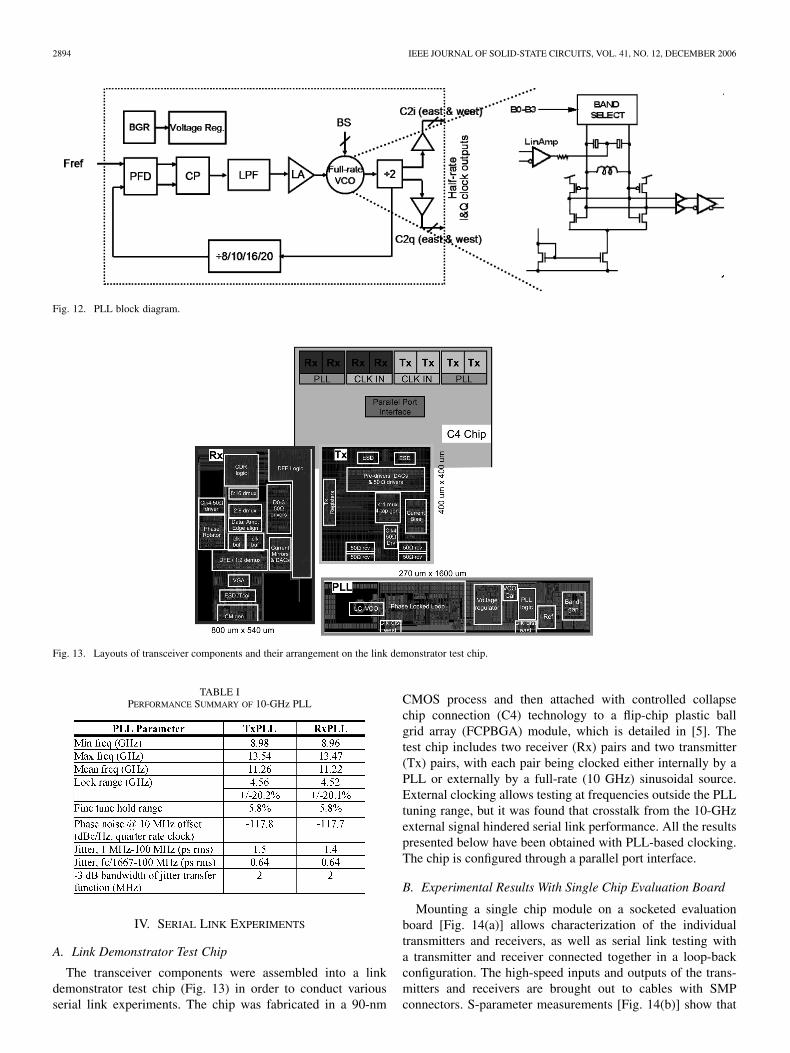
Fig. 13. Layouts of transceiver components and their arrangement on the link demonstrator test chip.
TABLE IPERFORMANCE SUMMARY OF 10-GHz PLL
IV. SERIAL LINK EXPERIMENTS
A. Link Demonstrator Test Chip
The transceiver components were assembled into a linkdemonstrator test chip (Fig. 13) in order to conduct variousserial link experiments. The chip was fabricated in a 90-nm
CMOS process and then attached with controlled collapsechip connection (C4) technology to a flip-chip plastic ballgrid array (FCPBGA) module, which is detailed in [5]. Thetest chip includes two receiver (Rx) pairs and two transmitter(Tx) pairs, with each pair being clocked either internally by aPLL or externally by a full-rate (10 GHz) sinusoidal source.External clocking allows testing at frequencies outside the PLLtuning range, but it was found that crosstalk from the 10-GHzexternal signal hindered serial link performance. All the resultspresented below have been obtained with PLL-based clocking.The chip is configured through a parallel port interface.
B. Experimental Results With Single Chip Evaluation Board
Mounting a single chip module on a socketed evaluationboard [Fig. 14(a)] allows characterization of the individualtransmitters and receivers, as well as serial link testing witha transmitter and receiver connected together in a loop-backconfiguration. The high-speed inputs and outputs of the trans-mitters and receivers are brought out to cables with SMPconnectors. S-parameter measurements [Fig. 14(b)] show that

BULZACCHELLI et al.: A 10-Gb/s 5-TAP DFE/4-TAP FFE TRANSCEIVER IN 90-nm CMOS TECHNOLOGY 2895
Fig. 14. (a) Photograph of single chip evaluation board. (b) S-parameter data showing combined loss of package (without socket), board, and 24-in of cable.
Fig. 15. Measured and simulated transmit eye diagrams at 10 Gb/s before (top)and after (bottom) applying one post-cursor of FFE.
the combined loss of module, evaluation board, and 24 in ofcable is 4 dB at 5 GHz (8 dB in loop-back testing). The ISIdue to this channel loss is readily observed in the transmit eyediagram at 10 Gb/s (top of Fig. 15). As shown in the figure,the measured eye diagram is similar to that calculated with thelink simulation tool from the S-parameter data. (The simulatedeye does not include random jitter.) Setting the FFE to normal-ized coefficients of [0, 0.85, 0.15, 0]) equalizes the channel(bottom of Fig. 15).
Receiver performance was studied with input data directlysupplied from a pseudo-random bit sequence generator. As anindicator of operating margins at 10 Gb/s, Fig. 16 shows plots ofthe receiver bit-error rate (BER) as a function of data samplingtime (often referred to as “bathtub curves”). To make these mea-surements, the CDR loop is frozen, and the phase rotator gen-erating the data sampling clock is manually swept over its posi-
tions (32 steps/UI). The DFE tap weights are also held at theirpreviously adapted values. With the DFE off (zero tap weights),the horizontal eye openings at a BER of 10 are 56% and 50%for input amplitudes of 1200 mVppd and 200 mVppd, respec-tively. These horizontal eye openings increase to 68.75% and62.5% upon application of the DFE, which helps equalize thechannel loss of the setup.
It should be noted that the bathtub curves of Fig. 16 are pes-simistic estimates of the receiver’s real performance. In normaloperation, low-frequency jitter from the receive PLL is trackedout by the CDR loop. With the CDR frozen, PLL jitter is nottracked out and directly impacts the estimates of horizontal eyeopening. Fig. 17 shows a histogram of the phase rotator’s po-sition in normal operation. The phase tracking provided by theCDR is a significant fraction of a UI, so the pessimism of themeasured bathtub curves is substantial. All of the bathtub curvesand estimates of horizontal eye opening presented in this paperare similarly pessimistic.
Connecting a transmitter’s outputs to a receiver’s inputsthrough a 16-in Tyco legacy backplane with HM-Zd edgeconnectors (loop-back configuration) is a demanding test ofthe transceiver’s equalization capabilities. S-parameter mea-surements [Fig. 18(a)] show that the combined loss of thesingle-chip evaluation board setup, the 16-in backplane, andthe cables (12 in from evaluation board to backplane, and 12 infrom backplane to evaluation board) is 33.5 dB at 5 GHz.The FFE tap weights are initially set to the values predictedby the high-level link simulation tool but are then fine tunedempirically for best link performance. After the DFE adaptationhas converged, the bathtub curve [Fig. 18(b)] is measured inthe manner explained above. The horizontal eye opening ofthe equalized signal is 22% at a BER of 10 , and error-freeoperation is obtained at eye center.
C. Chip-to-Chip Link Experiments
Directly soldering two modules on a board (Fig. 19) allowedserial link experiments from chip-to-chip. Boards fabricated inboth conventional and advanced technologies were used to com-pare performance so that the benefits of improved interconnectcould be assessed. The channels under test also differed in thetrace length between chips and in the number and types of via

2896 IEEE JOURNAL OF SOLID-STATE CIRCUITS, VOL. 41, NO. 12, DECEMBER 2006
Fig. 16. Measured bathtub curves of receiver.
Fig. 17. Histogram of phase rotator position with CDR active.
Fig. 18. Loop-back testing through 16-in Tyco legacy channel. (a) Channel frequency response. (b) Measured bathtub curve.
stubs. The first (#1) 10-in line was fabricated in conventionalboard technology, using Nelco 4000-13 material. The presenceof two 3.8-mm via stubs along the line results in signal reflec-tions, and the frequency response [Fig. 20(a)] exhibits a deepnotch near 8 GHz. At 5 GHz, the channel loss is 12 dB. The
second (#2) 10-in line was fabricated in an advanced technology,using lower loss APPE material. The sub-composite construc-tion of this board technology (described more fully in [5]) al-lows the via stub length to be reduced to 1.8 mm. With thevia stub resonant frequency more than doubled, the channel re-

BULZACCHELLI et al.: A 10-Gb/s 5-TAP DFE/4-TAP FFE TRANSCEIVER IN 90-nm CMOS TECHNOLOGY 2897
Fig. 19. Links used for chip-to-chip experiments.
Fig. 20. Frequency responses of channels used in chip-to-chip experiments. (a) 10-in (#1) line. (b) 10-in (#2) line. (c) 15-in line. (d) 20-in line.
sponse [Fig. 20(b)] has no deep notches in the frequency rangeof interest, and the loss at 5 GHz is 10 dB. The 15-in and 20-inlines were also fabricated in this advanced technology, thoughthe 15-in line was designed to be a difficult channel, with four3.8-mm and two 1.8-mm stubs. The frequency responses ofthese channels are plotted in Fig. 20(c) and (d).
The operating margins of these chip-to-chip links were eval-uated for three cases of equalization: FFE only, DFE only, andboth FFE and DFE. Fig. 21 shows how the choice of equaliza-tion affects the link margins at 10 Gb/s. With the highest lossat 5 GHz and bad reflections, the 15-in line is the most difficultto equalize, and only a combination of FFE and DFE is able toachieve a low BER. The first 10-in line also requires both FFEand DFE for a low BER. The other two lines (without bad reflec-tions) are easier to equalize, and a low BER is achieved for allthree cases of equalization. With both FFE and DFE employed,the horizontal eye openings approach 60%.
Fig. 21. Measured horizontal eye openings of four chip-to-chip links with dif-ferent equalizations applied.

2898 IEEE JOURNAL OF SOLID-STATE CIRCUITS, VOL. 41, NO. 12, DECEMBER 2006
V. SUMMARY
This paper has presented a 90-nm CMOS transceiver forchip-to-chip communications at 10 Gb/s. Using a 4-tap FFEand 5-tap DFE enables error-free NRZ signaling over channelswith more than 30 dB of loss. Design features such as half-rateclocking of the transmitter and receiver improve power effi-ciency. One transmitter/receiver pair and one PLL consume300 mW. The effectiveness of the FFE/DFE equalization hasbeen studied in serial link experiments using different typesof channels. These experiments not only demonstrate the per-formance of the transceiver but also highlight the importanceof reducing reflections due to structures such as via stubs, aslinks with bad reflections are often more difficult to equalizethan those with more loss. The use of more advanced boardtechnologies is one clear solution to the problem.
ACKNOWLEDGMENT
The authors wish to thank M. Sorna, S. Zier, P. Metty, andK. Heilmann from IBM Fishkill for valuable advice and assis-tance, and M. Oprysko and M. Soyuer from IBM Yorktown fortechnical and managerial support of this project.
REFERENCES
[1] “Common electrical I/O (CEI)—electrical and jitter interoperabilityagreements for 6+ Gb/s and 11+ Gb/s I/O,” Optical InterconnectForum, IA # OIF-CEI-02.0, Feb. 2005.
[2] T. Beukema, M. Sorna, K. Selander, S. Zier, B. L. Ji, P. Murfet, J.Mason, W. Rhee, H. Ainspan, B. Parker, and M. Beakes, “A 6.4-Gb/sCMOS SerDes core with feed-forward and decision-feedback equal-ization,” IEEE J. Solid-State Circuits, vol. 40, no. 12, pp. 2633–2645,Dec. 2005.
[3] R. Payne, P. Landman, B. Bhakta, S. Ramaswamy, S. Wu, J. D. Powers,M. U. Erdogan, A-L. Yee, R. Gu, L. Wu, Y. Xie, B. Parthasarathy,K. Brouse, W. Mohammed, K. Heragu, V. Gupta, L. Dyson, and W.Lee, “A 6.25-Gb/s binary transceiver in 0.13-�m CMOS for serialdata transmission across high loss legacy backplane channels,” IEEEJ. Solid-State Circuits, vol. 40, no. 12, pp. 2646–2657, Dec. 2005.
[4] K. Krishna, D. A. Yokoyama-Martin, A. Caffee, C. Jones, M.Loikkanen, J. Parker, R. Segelken, J. L. Sonntag, J. Stonick, S. Titus,D. Weinlader, and S. Wolfer, “A multigigabit backplane transceivercore in 0.13-�m CMOS with a power-efficient equalization architec-ture,” IEEE J. Solid-State Circuits, vol. 40, no. 12, pp. 2658–2666,Dec. 2005.
[5] L. Shan, Y. Kwark, P. Pepeljugoski, M. Meghelli, T. Beukema, C.Baks, J. Trewhella, and M. Ritter, “Design, analysis, and experimentalverification of an equalized 10 Gb/s link,” in Proc. DesignCon, SantaClara, CA, Feb. 2006.
[6] J. L. Zerbe, C. W. Werner, V. Stojanovic, F. Chen, J. Wei, G. Tsang,D. Kim, W. F. Stonecypher, A. Ho, T. P. Thrush, R. T. Kollipara, M.A. Horowitz, and K. S. Donnelly, “Equalization and clock recoveryfor a 2.5–10-Gb/s 2-PAM/4-PAM backplane transceiver cell,” IEEE J.Solid-State Circuits, vol. 38, no. 12, pp. 2121–2130, Dec. 2003.
[7] R. Farjad-Rad, C.-K. K. Yang, M. A. Horowitz, and T. H. Lee, “A 0.3-�m CMOS 8-Gb/s 4-PAM serial link transceiver,” IEEE J. Solid-StateCircuits, vol. 35, no. 5, pp. 757–764, May 2000.
[8] J. T. Stonick, G.-Y. Wei, J. L. Sonntag, and D. K. Weinlader, “An adap-tive PAM-4 5-Gb/s backplane transceiver in 0.25-�m CMOS,” IEEE J.Solid-State Circuits, vol. 38, no. 3, pp. 436–443, Mar. 2003.
[9] V. Stojanovic, “Channel-limited high-speed links: Modeling, analysisand design,” Ph.D. dissertation, Stanford Univ., Stanford, CA, 2004.
[10] N. Krishnapura, M. Barazande-Pour, Q. Chaudhry, J. Khoury, K. Lak-shmikumar, and A. Aggarwal, “A 5Gb/s NRZ transceiver with adaptiveequalization for backplane transmission,” in IEEE ISSCC Dig. Tech.Papers, San Francisco, CA, Feb. 2005, pp. 60–61.
[11] T. Schafbauer et al., “Integration of high-performance, low-leakage,and mixed signal features into a 100 nm CMOS technology,” in Symp.VLSI Technology Dig. Tech. Papers, Honolulu, HI, Jun. 2002, pp.62–63.
[12] G. Scott, J. Lutze, M. Rubin, F. Nouri, and M. Manley, “NMOS drivecurrent reduction caused by transistor layout and trench isolation in-duced stress,” in IEDM Tech. Dig., Washington, DC, Dec. 1999, pp.827–830.
[13] M. Anis, M. Allam, and M. Elmasry, “Impact of technology scaling onCMOS logic styles,” IEEE Trans. Circuits Syst. II, Analog Digit. SignalProcess., vol. 49, no. 8, pp. 577–588, Aug. 2002.
[14] A. Rylyakov and S. Rylov, “A low power 10 Gb/s serial link trans-mitter in 90-nm CMOS,” in IEEE Compound Semiconductor IC Symp.(CSICS) Tech. Dig., Palm Springs, CA, Oct./Nov. 2005, pp. 189–191.
[15] M. Meghelli, “A 43-Gb/s full-rate clock transmitter in 0.18-�m SiGeBiCMOS technology,” IEEE J. Solid-State Circuits, vol. 40, no. 10, pp.2046–2050, Oct. 2005.
[16] C. Menolfi, T. Toifl, R. Reutemann, M. Ruegg, P. Buchmann, M.Kossel, T. Morf, and M. Schmatz, “A 25 Gb/s PAM4 transmitter in 90nm CMOS SOI,” in IEEE ISSCC Dig. Tech. Papers, San Francisco,CA, Feb. 2005, pp. 72–73.
[17] S. Galal and B. Razavi, “Broadband ESD protection circuits inCMOS technology,” IEEE J. Solid-State Circuits, vol. 38, no. 12, pp.2334–2340, Dec. 2003.
[18] S. Sidiropoulos and M. A. Horowitz, “A semidigital dual delay-lockedloop,” IEEE J. Solid-State Circuits, vol. 32, no. 11, pp. 1683–1692,Nov. 1997.
[19] J. Chen and B. Shi, “Novel constant transconductance references andthe comparisons with the traditional approach,” in Proc. SouthwestSymp. Mixed-Signal Design, Las Vegas, NV, Feb. 2003, pp. 104–107.
[20] S. Kasturia and J. H. Winters, “Techniques for high-speed implemen-tation of nonlinear cancellation,” IEEE J. Sel. Areas Commun., vol. 9,no. 6, pp. 711–717, Jun. 1991.
[21] M. Meghelli, S. Rylov, J. Bulzacchelli, W. Rhee, A. Rylyakov, H.Ainspan, B. Parker, M. Beakes, A. Chung, T. Beukema, P. Pepelju-goski, L. Shan, Y. Kwark, S. Gowda, and D. Friedman, in IEEE ISSCCDig. Tech. Papers, Feb. 2006, pp. 80–81.
John F. Bulzacchelli (S’92–M’02) was born in NewYork, NY, in 1966. He received the S.B., S.M., andPh.D. degrees in electrical engineering, all from theMassachusetts Institute of Technology (MIT), Cam-bridge, in 1990, 1990, and 2003, respectively.
From 1988 to 1990, he was a co-op studentat Analog Devices, Wilmington, MA, where heinvented a new type of delay-and-phase-lockedloop for high-speed clock recovery. From 1992 to2002, he conducted his doctoral research at the IBMT. J. Watson Research Center, Yorktown Heights,
NY, in a joint study program between IBM and MIT. In his doctoral work, hedesigned and demonstrated a superconducting bandpass delta-sigma modulatorfor direct A/D conversion of multi-GHz RF signals. In 2003, he became aResearch Staff Member at the same IBM location, where his primary job is thedesign of mixed-signal CMOS circuits for high-speed data communications.He also maintains strong interest in the design of circuits in more exploratorytechnologies. He holds two U.S. patents.
Dr. Bulzacchelli received the Jack Kilby Award for Outstanding StudentPaper at the 2002 IEEE International Solid-State Circuits Conference.
Mounir Meghelli was born in Oran, Algeria in1969. He received the M.S. degree in electronicsand automatics from the University of Paris XI,France, in 1992, and the Engineering degree inTelecommunication from the ENST-Paris in 1994.From 1994 to 1998, he was with the France TelecomResearch Center, CNET-Bagneux, as a Ph.D. studentworking on the design of high-speed ICs.
Since 1998, he has been with the IBM T. J. WatsonResearch Center, Yorktown Heights, NY, working onthe design of SiGe BiCMOS and CMOS high-speed
integrated circuits.
BULZACCHELLI et al.: A 10-Gb/s 5-TAP DFE/4-TAP FFE TRANSCEIVER IN 90-nm CMOS TECHNOLOGY 2899
Sergey V. Rylov (M’05) received the M.S. and Ph.D.degrees in physics from Moscow State University,Moscow, Russia, in 1984 and 1987, respectively.
Until 1991, he worked as a Research Scientistwith the Laboratory of Cryoelectronics, MoscowState University. His research was in the field of su-perconducting Josephson junction microelectronics,particularly single-flux-quantum digital devices,analog-to-digital converters (ADCs), and physicallyreversible computers. From 1991 to 1998, he waswith HYPRES, Inc., where he successfully designed
many high-performance superconducting digital and analog devices, includinghigh-resolution and flash ADCs, single-flux-quantum logic devices, and analogamplifiers using DC SQUIDs. Since 1998, he has been with the IBM T. J.Watson Research Center, Yorktown Heights, NY, where he currently workson circuit design of high-speed digital and mixed-signal devices for CMOScommunications ICs.
Woogeun Rhee (S’93–A’98–M’00) received theB.S. degree in electronics engineering from SeoulNational University, Seoul, Korea, in 1991, the M.S.degree in electrical engineering from the Universityof California at Los Angeles in 1993, and the Ph.D.degree in electrical and computer engineering fromthe University of Illinois at Urbana-Champaign in2001.
From 1997 to 2001, he was with Conexant Sys-tems, Newport Beach, CA, where he was a PrincipalEngineer in the frequency synthesizer design group.
Since 2001, he has been a Research Staff Member at the IBM T. J. Watson Re-search Center, Yorktown Heights, NY. His current interests are in phase-lockedloops and clock-and-data recovery circuits for high-speed I/O interfaces, andin low-power RF circuits with emphasis on frequency synthesizers for wirelesscommunications.
Alexander V. Rylyakov received the M.S. degreein physics from the Moscow Institute of Physics andTechnology, Moscow, Russia, in 1989, and the Ph.D.degree in physics from the State University of NewYork (SUNY) at Stony Brook in 1997.
From 1994 to 1999, he worked in the Departmentof Physics at SUNY Stony Brook on the design andtesting of high-speed (up to 770 GHz) digital inte-grated circuits based on a superconductor Josephsonjunction technology. In 1999, he joined the IBM T. J.Watson Research Center, Yorktown Heights, NY, as a
Research Staff Member, working on the design and testing of full-custom digitaland mixed signal integrated circuits for serial communications (up to 80 Gb/sdata rates and up to 100 GHz clock rates), using a broad spectrum of CMOSand SiGe technologies.
Herschel A. Ainspan received the B.S. and M.S. degrees in electrical en-gineering from Columbia University, New York, NY, in 1989 and 1991,respectively.
In 1989, he joined the IBM Thomas J. Watson Research Center, YorktownHeights, NY, where he has been involved in the design of mixed-signal and RFICs for high-speed data communications.
Benjamin D. Parker received the B.S. degree inphysics from Bowdoin College, Brunswick, ME, in1979, and the M.S. degree in physics from BrownUniversity, Providence, RI, in 1981. His graduatework dealt with the optical properties of adsorbedlayers on metal surfaces.
In 1986, he joined the GaAs group at the IBMT. J. Watson Research Center, Yorktown Heights,NY, where he worked on characterization of III–Vsemiconductor systems. In 1991, he joined theMixed-Signal Communications IC Design Group,
working on design and verification of high-speed serial communication links.
Michael P. Beakes (S’79–M’80) is a Senior En-gineer at the IBM T. J. Watson Research Center,Yorktown Heights, NY. Throughout his 26-yearcareer at IBM, he has been involved in customcircuit design, design automation, and education. Heis also a Mentor and Advisor for grade school andhigh school technology and robotics programs. Hiseducational background includes physics, electricalengineering, and computer engineering.
Aichin Chung received the B.A.Sc. degree in elec-trical engineering from the University of Waterloo,Waterloo, ON, Canada, in 2000, and the M.A.Sc. de-gree in electrical engineering from the University ofToronto, Toronto, ON, Canada, in 2003.
She is currently working at the IBM T. J. WatsonResearch Center, Yorktown Heights, NY, in theMixed Signal Communications IC Design depart-ment. Her current focus is on high-speed circuitdesign for I/O backplanes and the developmentand support of custom EDA tools for advanced
technology designs.Ms. Chung was the recipient of the 2003 BiCMOS/Bipolar Circuits and Tech-
nology Meeting Outstanding Student Paper Award.
TroyJ.Beukema received the B.S.E.E. and M.S.E.E.degrees from Michigan Technological University,Houghton, in 1984 and 1988, respectively.
From 1984 to 1988, he was an R&D Engineer atHewlett-Packard in the area of communications testequipment. He joined Motorola CommunicationsSector, Schaumburg, IL, in 1989 and contributedto the development of digital cellular wireless sys-tems. In 1996, he joined IBM Research, YorktownHeights, NY, where he is involved in the areas ofintegrated 60 GHz wireless system designs and
high-speed serial I/O core architecture for adaptive equalization of 6–12 Gb/sbackplane/wireline links. His research interests include communication linksystem design and simulation, with an emphasis on modulation, equalization,and synchronization for wireless and high-speed wireline channels.
Petar K. Pepeljugoski (S’91–M’92–SM’03) re-ceived the B.Sc. degree from Ss. Cyril and MethodiusUniversity, Skopje, Macedonia, in 1982, the M.S.degree from the University of Belgrade, Belgrade,Yugoslavia, in 1986, and the Ph.D. degree from theUniversity of California at Berkeley in 1993.
He is a Research Staff Member in the Communi-cation Technology Department at the IBM ThomasJ. Watson Research Center, Yorktown Heights, NY.He joined IBM in 1994, where his research work in-cluded design, modeling, prototyping, and character-
ization of high-speed multimode fiber LAN links and parallel interconnects, as

2900 IEEE JOURNAL OF SOLID-STATE CIRCUITS, VOL. 41, NO. 12, DECEMBER 2006
well as the use of equalization in electrical and optical links. He was also in-volved in 802.3 projects (802.3z, 802.3ae, 802.3aq) and the Call For Interest forEthernet Higher Speed Study Group in July 2006. He is an author or co-authorof more than 50 journal or conference articles.
Lei Shan (S’00–M’01) received the M.S. degreein electrical engineering and the Ph.D. degree inmechanical engineering from the Georgia Instituteof Technology, Atlanta, in 2000.
From 1997 to 2000, he was studying the tribolog-ical aspects of the chemical mechanical polishingprocess for microelectronics fabrication, as a grad-uate assistant at Georgia Tech. In January 2001,he joined the IBM T. J. Watson Research Center,Yorktown Heights, NY, as a Research Staff Member,where he works on high-speed electronics/opto-
electronics packaging designs as well as electrical and thermal modeling. Hedesigned and demonstrated high-speed packages on both connectorized formatand IBM ceramic BGA for 50 Gb/s multiplexers and demultiplexers based onIBM SiGe BiCMOS technology. He has authored over 30 papers.
Dr. Shan received the 1999 Best Paper Award from the Journal of Tribologyand the Best Paper Award of DesignCon 2005.
Young H. Kwark (S’80–M’82) received the B.S. de-gree in electrical engineering from the MassachusettsInstitute of Technology, Cambridge, and the M.S. andPh.D. degrees in electrical engineering from StanfordUniversity, Stanford, CA.
His work experience as a Research Staff Memberat the IBM T. J. Watson Research Center, YorktownHeights, NY, includes circuit design for optical linksand wireless applications. He is currently involved inpackage characterization for high-performance com-puting platforms.
Sudhir Gowda (S’88–M’91) received the B.Tech.degree in electrical engineering from the IndianInstitute of Technology, Madras, India, in 1987, andthe M.S. and Ph.D. degrees in electrical engineeringfrom the University of Southern California, LosAngeles, CA, in 1989 and 1992, respectively.
At the University of Southern California, heworked on the development of the BSIM+ sub-micron MOS model for analog and digital VLSIcircuits. He also conducted research in microelec-tronic circuit reliability simulation. In December
1992, he joined IBM Corporation, Thomas J. Watson Research Center, York-town Heights, NY, where he is currently Senior Manager, CommunicationCircuits and Systems Department. While with IBM, he has worked on thedesign of infrared transceivers, disk drive read channels, CMOS imagers, andhigh-speed interconnect circuits. His research interests include architecturaldesign and detailed circuit implementations for high-speed interconnect andcommunications applications. He has published over 30 technical articles andholds 12 patents.
Daniel J. Friedman (S’91–M’92) received the Ph.D.degree in engineering science from Harvard Univer-sity, Cambridge, MA, in 1992.
After completing consulting work at MIT LincolnLabs and postdoctoral work at Harvard in imagesensor design, he joined the IBM Thomas J. WatsonResearch Center, Yorktown Heights, NY, in 1994.His initial work at IBM was the design of analogcircuits and air interface protocols for field-poweredRFID tags. In 1999, he turned his focus to analogcircuit design for high-speed serial data communi-
cation. Since June 2000, he has managed a team of circuit designers workingon serial data communication, wireless, and PLL applications. In addition tocircuits papers regarding serial links, he has published articles on imagersand RFID, and he holds more than 20 patents. His current research interestsinclude high-speed I/O design, PLL design, and circuit/system approaches forvariability compensation.