Embed Size (px)
Citation preview
HVDC system based on Cockcroft-Walton generatorJ.F.A.P. Cunha, MSc Student, IST, S.P.F. Pinto, IST, J.F.A Silva, IST
Abstract—In this work, a study was carried out to design athree-phase AC-DC boost converter based on Cockcroft-Walton,converting a three-phase voltage to voltage levels of a HVDCsystem. The Cockcroft-Walton converter is connected to the gridusing a matrix converter, taking advantage of its ability to controlthe output frequency, as well as the ability to transform thethree-phase AC voltages and currents into a single-phase voltageand current. A closed-loop controller is designed to control theoutput voltage with an inner current loop, ensuring an unitarypower factor in the AC side. Using the simulation softwareMATLAB/Simulink, the converter is tested to verify and validatethe proposed converter, and the obtained results are discussed.
Index terms - Cockcroft-Walton converter, AC-DC converter,HVDC, Matrix converter, Voltage controller
I. INTRODUCTION
Through the years, society has become more dependent onelectric energy, and with the environment being an importantissue to the political agenda, there has been increased researchfor cleaner energy, through renewable energy sources, wherewind power is one of the most promising [1]. As most ofthe best locations onshore for wind farms are taken, offshoreturbines presents a good alternative, as the average wind speedis 20% higher revealing a better exploitation potential of thewind resource.
Usually, in land, the electric power transmission is inalternating current, but due to the reactive power generatedin submarines cables, over long distances, it is crucial to usea High Voltage Direct Current (HVDC) system. Given futureinvestments on offshore wind farms, this work is focused ona new topology to achieve voltage levels of a HVDC systembased on a matrix converter and the Cockcroft-Walton (CW)voltage multiplier.
The necessary steps to achieve that are the following:• Study the operation of Cockcroft-Walton converter;• Study the operation of matrix converter;• Study the principle of operation and design of the pro-
posed converter;• Study and design the control system of CW converter
output voltage, from current control;• Simulate the proposed converter using MAT-
LAB/Simulink software;
II. COCKCROFT-WALTON VOLTAGE MULTIPLIER
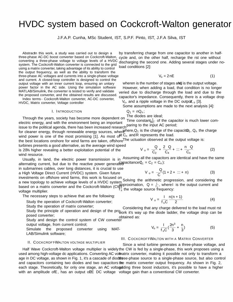
Half Wave Cockcroft-Walton voltage multiplier is widelyused among high-voltage dc applications. Converting AC volt-age in DC voltage, as shown in Fig. 1, it’s a cascade of diodesand capacitors containing two diodes and two capacitors ineach stage. Theoretically, for only one stage, an AC voltagewith an amplitude of E, has an output of 2E DC voltage
by transferring charge from one capacitor to another in half-cycle and, on the other half, recharge the first one withoutdischarging the second one. Adding several stages under no-load conditions [2]:
Vo = 2nE (1)
where n is the number of stages and Vo is the output voltage.However, when adding a load, that condition is no longer
verified due to discharge through the load and due to thecapacitor’s impedance. Consequently, there is a voltage drop∆Vo, and a ripple voltage in the DC output, δVo [3].
Some assumptions are made to the next analysis [4]:• Q1 = nQn;• The diodes are ideal;• Time constant 1
RC of the capacitor is much lower com-paring to the input AC period;
where, Q1 is the charge of the capacitor C1, Qn the chargeat Cn and R represents the load.
The fluctuation observed at the output voltage is:
δVo =∆Q
C2+
2∆Q
C4+ ...+
n∆Q
Cn(2)
Assuming all the capacitors are identical and have the samecapacitance (C1 = C2 = Cn):
δVo =∆Q
C(1 + 2 + ...+ n) (3)
Solving the arithmetic progression, and considering theapproximation, ∆Q = I
fs, where I is the output current and
fs the voltage source frequency:
δVo =I
fsC
n(n+ 1)
2(4)
Considering that any charge delivered to the load must firstwork it’s way up the diode ladder, the voltage drop can beobtained as:
∆Vo =I
fsC(2n3
3+n
3) (5)
III. COCKCROFT-WALTON WITH A MATRIX CONVERTER
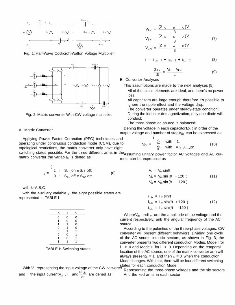
Since a wind turbine generates a three-phase voltage, andthe CW is fed by a single-phase, this work proposes using amatrix converter, making it possible not only to transform athree-phase source to a single-phase source, but also controlthe matrix converter output frequency. As shown in Fig. 2,adding three boost inductors, it’s possible to have a highervoltage gain than a conventional CW converter.
Vin
− +VC1
D1 D2
+−VC2
A
G
B
C
...
...
...
D(2n−1)
− +
VC(2n−1)
D2n
− +VC2n
R
+−Vo
Fig. 1: Half-Wave Cockcroft-Walton Voltage Multiplier.
Va
Vb
Vc
+ −VLa
iLa
+ −VLb
iLb
+ −VLc
iLc
− +VC1
iγ
D1 D2
+−VC2
...
...
...
D(2n−1)
− +
VC(2n−1)
D2n
− +VC2n
R
+−Vo
SA1 SB1 SC1
SA2 SB2 SC2
N
A
B
C
+
Vγ
−
Fig. 2: Matrix converter With CW voltage multiplier.
A. Matrix Converter
Applying Power Factor Correction (PFC) techniques andoperating under continuous conduction mode (CCM), due totopological restrictions, the matrix converter only have eightswitching states possible. For the three different arms in thematrix converter the variable γk is defined as
γk =
1 → Sk1 on e Sk2 off.0 → Sk1 off e Sk2 on.
(6)
with k=A,B,C.with the auxiliary variable γk, the eight possible states are
represented in TABLE I
γA γB γC
0 0 01 0 01 1 00 1 00 1 10 0 11 0 11 1 1
TABLE I: Switching states
With Vγ representing the input voltage of the CW converter
and iγ the input current, VkN
, iγ anddiLkdt
are defined as
VAN =(2γA − γB − γC)Vγ
3
VBN =(2γB − γC − γA)Vγ
3(7)
VCN =(2γC − γA − γB)Vγ
3
iγ = iLaγA + iLbγB + iLcγC (8)
diLkdt
=Vk − VkN
L(9)
B. Converter Analyses
This assumptions are made to the next analyses [5]• All of the circuit elements are ideal, and there’s no power
loss;• All capacitors are large enough therefore it’s possible to
ignore the ripple effect and the voltage drop;• The converter operates under steady-state condition;• During the inductor demagnetization, only one diode will
conduct;• The three-phase ac source is balanced;Defining the voltage in each capacitors (VCi) in order of the
output voltage and number of stages, VCi can be expressed as
VCi =
Vo
2n , with i=1.Vo
n , with i = 2,3,...,2n.(10)
Assuming unitary power factor AC voltages and AC cur-rents can be expressed as
Va = Vmsinωt
Vb = Vmsin(ωt+ 120) (11)Vc = Vmsin(ωt− 120)
iLA = Imsinωt
iLB = Imsin(ωt+ 120) (12)iLC = Imsin(ωt− 120)
Where Vm and Im are the amplitude of the voltage and thecurrent respectively, and ω the angular frequency of the ACsource.
According to the polarities of the three-phase voltages, CWconverter will present different behaviors. Dividing one cycleof the AC source into six sectors, as shown in Fig. 3, theconverter presents two different conduction Modes. Mode I foriγ < 0 and Mode II for iγ > 0. Depending on the temporallocation of the AC source, one of the matrix converter arm willalways present γk = 1 and then γk = 0 when the conductionMode changes. With that, there will be four different switchingstates for each conduction Mode.
Representing the three-phase voltages and the six sectorsAnd the fixed arms in each sector
t
V
V aV bV c
30 90 150 210 270 330
Fig. 3: AC source voltages.
Sector θ[] Brao Fixo
I -30 ∼ 30 γAII 30 ∼ 90 γBIII 90 ∼ 150 γCIV 150 ∼ 210 γAV 210 ∼ 270 γBVI 270 ∼ 330 γC
TABLE II: Sector and fixed arm
Analyzing sector I for both Modes it’s possible to determi-
nate the slopes ofdiLbdt
anddiLcdt
.
For Mode I, with γA = 0 and Vγ = −Vo
2n , making use ofequations (7) (8) and (9) the operation of the four circuit statescan be detailed as
Va
Vb
Vc
+ −VLa
iLa
+ −VLb
iLb
+ −VLc
iLc
− +VC1
iγ
D1 D2
+−VC2
...
...
...
D(2n−1)
− +
VC(2n−1)
D2n
− +VC2n
R
+−Vo
SA1 SB1 SC1
SA2 SB2 SC2
N
A
B
C
+
Vγ
−
Fig. 4: Sector I Mode I State 1.
VkN =
VBN = −1
3
Vo2n
VCN = −1
3
Vo2n
(13)
iγ = ib + ic = −ia (14)
diLkdt
=
diLbdt
=Vb +
1
3
Vo2n
L
diLcdt
=Vc +
1
3
Vo2n
L
(15)
Va
Vb
Vc
+ −VLa
iLa
+ −VLb
iLb
+ −VLc
iLc
− +VC1
iγ
D1 D2
+−VC2
...
...
...
D(2n−1)
− +
VC(2n−1)
D2n
− +VC2n
R
+−Vo
SA1 SB1 SC1
SA2 SB2 SC2
N
A
B
C
+
Vγ
−
Fig. 5: Sector I Mode I State 2.
VkN =
VBN =
1
3
Vo2n
VCN = −2
3
Vo2n
(16)
iγ = ic (17)
diLkdt
=
diLbdt
=Vb −
1
3
Vo2n
L
diLcdt
=Vc +
2
3
Vo2n
L
(18)
Va
Vb
Vc
+ −VLa
iLa
+ −VLb
iLb
+ −VLc
iLc
− +VC1
iγ
D1 D2
+−VC2
...
...
...
D(2n−1)
− +
VC(2n−1)
D2n
− +VC2n
R
+−Vo
SA1 SB1 SC1
SA2 SB2 SC2
N
A
B
C
+
Vγ
−
Fig. 6: Sector I Mode I State 3.
VkN =
VBN = −2
3
Vo2n
VCN =1
3
Vo2n
(19)
iγ = ib (20)
diLkdt
=
diLbdt
=Vb +
2
3
Vo2n
L
diLcdt
=Vc −
1
3
Vo2n
L
(21)
Va
Vb
Vc
+ −VLa
iLa
+ −VLb
iLb
+ −VLc
iLc
− +VC1
iγ
D1 D2
+−VC2
...
...
...
D(2n−1)
− +
VC(2n−1)
D2n
− +VC2n
R
+−Vo
SA1 SB1 SC1
SA2 SB2 SC2
N
A
B
C
+
Vγ
−
Fig. 7: Sector I Mode I State 4.
VkN =
VBN = 0
VCN = 0(22)
iγ = 0 (23)
diLkdt
=
diLbdt
=VbL
diLcdt
=VcL
(24)
For Mode II, with γA = 1, the polarities of the diodeschange having now Vγ = Vo
2n
Va
Vb
Vc
+ −VLa
iLa
+ −VLb
iLb
+ −VLc
iLc
− +VC1
iγ
D1 D2
+−VC2
...
...
...
D(2n−1)
− +
VC(2n−1)
D2n
− +VC2n
R
+−Vo
SA1 SB1 SC1
SA2 SB2 SC2
N
A
B
C
+
Vγ
−
Fig. 8: Sector I Mode II State 1.
VkN =
VBN = 0
VCN = 0(25)
iγ = 0 (26)
diLkdt
=
diLbdt
=VbL
diLcdt
=VcL
(27)
VkN =
VBN = −2
3
Vo2n
VCN =1
3
Vo2n
(28)
iγ = −ib (29)
Va
Vb
Vc
+ −VLa
iLa
+ −VLb
iLb
+ −VLc
iLc
− +VC1
iγ
D1 D2
+−VC2
...
...
...
D(2n−1)
− +
VC(2n−1)
D2n
− +VC2n
R
+−Vo
SA1 SB1 SC1
SA2 SB2 SC2
N
A
B
C
+
Vγ
−
Fig. 9: Sector I Mode II State 2.
diLkdt
=
diLbdt
=Vb +
2
3
Vo2n
L
diLcdt
=Vc −
1
3
Vo2n
L
(30)
Va
Vb
Vc
+ −VLa
iLa
+ −VLb
iLb
+ −VLc
iLc
− +VC1
iγ
D1 D2
+−VC2
...
...
...
D(2n−1)
− +
VC(2n−1)
D2n
− +VC2n
R
+−Vo
SA1 SB1 SC1
SA2 SB2 SC2
N
A
B
C
+
Vγ
−
Fig. 10: Sector I Mode II State 3.
VkN =
VBN =
1
3
Vo2n
VCN = −2
3
Vo2n
(31)
iγ = −ic (32)
diLkdt
=
diLbdt
=Vb −
1
3
Vo2n
L
diLcdt
=Vc +
2
3
Vo2n
L
(33)
VkN =
VBN = −1
3
Vo2n
VCN = −1
3
Vo2n
(34)
iγ = ia (35)

Va
Vb
Vc
+ −VLa
iLa
+ −VLb
iLb
+ −VLc
iLc
− +VC1
iγ
D1 D2
+−VC2
...
...
...
D(2n−1)
− +
VC(2n−1)
D2n
− +VC2n
R
+−Vo
SA1 SB1 SC1
SA2 SB2 SC2
N
A
B
C
+
Vγ
−
Fig. 11: Sector I Mode II State 4.
diLkdt
=
diLbdt
=Vb +
1
3
Vo2n
L
diLcdt
=Vc +
1
3
Vo2n
L
(36)
Completed the analyses for Sector I, the same procedureis applied for the remaining Sectors. Through TABLE III allpossible states describe the behavior of each one of the three-phase currents.
C. Output Voltage Control
To achieve unitary power factor and the wanted voltagelevel, this work uses a closed-loop controller. Using an outervoltage loop and since the dynamics of the output voltage ismuch slower than the input current, the output voltage controlis done by slowly varying the reference input current throughan inner current loop [6]. Comparing the output voltage with avoltage reference, Vref , an error will be generated. Feeding theerror into a proportional-integral compensator will generate therequired amplitude for the three-phase currents. Synchronizingthe required amplitude signal and comparing with the three-phase currents three errors will be generated. According tothose errors and depending on the Sector and Mode signals theswitching state is chosen using TABLE III. In order to improvethe output voltage ripple, through equation (4), increasing theoutput matrix converter frequency, the ripple will decrease.
++Voref Tzs +1
TpsCompensador
GTds +1
ILk RsR(C/n)+1
Vo
H
-
Fig. 12: Block diagram of the voltage controller.
D. Design Considerations
1) Capacitor voltage stress and capacitance: Accordingto equation (10), the voltage stress across C1 is Vo
2n and theremaining capacitors Vo
n . For the determination of the capaci-tance, the output voltage ripple is used as the design criteria.
Sector Mode State γA γBdiLb
dtγC
diLc
dtiγ
I
I
1
0
1 + 1 + -iLa < 02 0 - 1 + iLc < 03 1 + 0 - iLb < 04 0 - 0 - 0
II
1
1
1 - 1 - 02 0 + 1 - -iLb > 03 1 - 0 + -iLc > 04 0 + 0 + iLa > 0
γB γAdiLa
dtγC
diLc
dt
II
I
1
1
1 + 1 + 02 0 - 1 + -iLa < 03 1 + 0 - -iLc < 04 0 - 0 - iLb < 0
II
1
0
1 - 1 - -iLb > 02 0 + 1 - iLc > 03 1 - 0 + iLa > 04 0 + 0 + 0
γC γAdiLa
dtγB
diLb
dt
III
I
1
0
1 + 1 + -iLc < 02 0 - 1 + iLb < 03 1 + 0 - iLa < 04 0 - 0 - 0
II
1
1
1 - 1 - 02 0 + 1 - -iLa > 03 1 - 0 + -iLb > 04 0 + 0 + iLc > 0
γA γBdiLb
dtγC
diLc
dt
IV
I
1
1
1 + 1 + 02 0 - 1 + -iLb < 03 1 + 0 - -iLc < 04 0 - 0 - iLa < 0
II
1
0
1 - 1 - -iLa > 02 0 + 1 - iLc > 03 1 - 0 + iLb > 04 0 + 0 + 0
γB γAdiLa
dtγC
diLc
dt
V
I
1
0
1 + 1 + -iLb < 02 0 - 1 + iLc < 03 1 + 0 - iLa < 04 0 - 0 - 0
II
1
1
1 - 1 - 02 0 + 1 - -iLa > 03 1 - 0 + -iLc > 04 0 + 0 + iLb > 0
γC γAdiLa
dtγB
diLb
dt
VI
I
1
1
1 + 1 + 02 0 - 1 + -iLa < 03 1 + 0 - -iLb < 04 0 - 0 - iLc < 0
II
1
0
1 - 1 - -iLc > 02 0 + 1 - iLb > 03 1 - 0 + iLa > 04 0 + 0 + 0
TABLE III: Currents slope
Through equation (4), and switching the source frequency fswith the matrix converter output frequency fo, the capacitancecan be calculated as
C =io
foδVo,fo
n(n+ 1)
2(37)
2) Boost inductor: Even the topology of the proposedconverter is different from traditional boost-type rectifiers, the

switching strategies can easily adapt, so the design criteriaof the boost inductors are also available for the proposedconverter [5].
L =
√3Vmton,min∆iLk,max
(38)
with ton,min the minimum turn on time of the switches and∆iLk,max the expected percentage of the maximum peak-to-peak ripple.
3) Voltage and Current stresses on switches and diodes:Assuming unitary efficiency, the current stress on switches anddiodes can be derived as
iLkef =Po
3Vkef(39)
with iLkef and Vkef representing the current and the voltagerms value and Po the output power.
The voltage stress across the switches and diodes can becalculated by equation (40) and (41) respectively
VImax =Vo,max
2n(40)
VDmax =Vo,maxn
(41)
E. Simulations
Through the MATLAB/Simulink software, a simulation ismade of the matrix converter and the CW voltage multiplierproposed topology. Aiming to convert 690V phase-phase volt-age generated by a wind turbine to 200kV DC voltage, dueto computational limitations, the Cockcroft-Walton will havea limit of 50 stages. The system specification for the proposedconverter is summarized as follows:
Parameters Value Units
Vo 200, 000 Vfo 4, 000 HzR 20, 000 ΩPo 2, 000, 000 Wn 50Lk 0.181 mHCi 50.731 µF
TABLE IV: Circuit parameters
Analyzing Fig. 13, there is an initial discharge in thecapacitors, because it starts with an initial voltage close to thefinal one, occurring subsequently the transitory until it reachesthe 200kV voltage. Zooming-in the steady state of the outputvoltage in Fig. 14, it is possible to observe an output voltageripple of about 10kV, representing 5% of the mean outputvalue.
Observing Fig. 15, the unitary power factor is achieved,validating the PFC techniques used.
0 0.5 1 1.50
1
2
3
x 105
Tempo (s)
Vo (V
)
Fig. 13: Output voltage.
1.43 1.44 1.45 1.46 1.47 1.48 1.491.8
1.9
2
2.1
x 105
Tempo (s)
Vo (V
)
Fig. 14: Zoom-in in the voltage output waveform.
1.3 1.35 1.4 1.45 1.5−2000
−1000
0
1000
2000
Tempo (s)Va
(V)
(a) Phase A voltage
1.3 1.35 1.4 1.45 1.5−5000
0
5000
Tempo (s)
iLa
(A)
(b) Phase A current
Fig. 15: Voltage and current in fase A.
IV. CONCLUSIONS
In this study, a three-phase AC-DC boost converter based onCockcroft-Walton was designed to convert 690V AC phase-to-phase to 200 kV DC. Using a matrix converter it was possibleto convert a three-phase voltage into a single-phase and tocontrol the matrix converter output frequency, reducing theoutput ripple to 5% of the mean output voltage value. Thematrix converter input current shows a sinusoidal wave and anearly unitary power factor validating the control techniquesused. With a Cockcroft-Walton converter with 50 stages it waspossible to achieve the desired output voltage of 200 kV
REFERENCES
[1] Rui MG Castro. Energias renovaveis e producao descentralizada–introducao a energia eolica. Lisboa, Universidade Tecnica deLisboa, 86p, 2007.

[2] Melvin M Weiner. Analysis of cockcroft-walton voltage multi-pliers with an arbitrary number of stages. Review of ScientificInstruments, 40(2):330–333, 1969.
[3] Ioannis C Kobougias and Emmanuel C Tatakis. Optimal designof a half-wave cockcroft–walton voltage multiplier with mini-mum total capacitance. Power Electronics, IEEE Transactionson, 25(9):2460–2468, 2010.
[4] JS Brugler. Theoretical performance of voltage multiplier cir-cuits. Solid-State Circuits, IEEE Journal of, 6(3):132–135, 1971.
[5] Chung-Ming Young, Hong-Lin Chen, and Ming-Hui Chen. Acockcroft–walton voltage multiplier fed by a three-phase-to-single-phase matrix converter with pfc. IEEE Transactions onIndustry Applications, 50(3):1994–2004, 2014.
[6] Jose Fernando Alves Silva. Electronica industrial–semicondutores e conversores de potencia. Fundacao CalousteGulbenkian, 2a edicao, 2013.