Embed Size (px)
Citation preview

HSPICE® Reference Manual: MOSFET ModelsVersion D-2010.12, December 2010

ii HSPICE® Reference Manual: MOSFET ModelsD-2010.12
Copyright Notice and Proprietary InformationCopyright © 2010 Synopsys, Inc. All rights reserved. This software and documentation contain confidential and proprietary information that is the property of Synopsys, Inc. The software and documentation are furnished under a license agreement and may be used or copied only in accordance with the terms of the license agreement. No part of the software and documentation may be reproduced, transmitted, or translated, in any form or by any means, electronic, mechanical, manual, optical, or otherwise, without prior written permission of Synopsys, Inc., or as expressly provided by the license agreement.
Right to Copy DocumentationThe license agreement with Synopsys permits licensee to make copies of the documentation for its internal use only. Each copy shall include all copyrights, trademarks, service marks, and proprietary rights notices, if any. Licensee must assign sequential numbers to all copies. These copies shall contain the following legend on the cover page:
“This document is duplicated with the permission of Synopsys, Inc., for the exclusive use of __________________________________________ and its employees. This is copy number __________.”
Destination Control StatementAll technical data contained in this publication is subject to the export control laws of the United States of America. Disclosure to nationals of other countries contrary to United States law is prohibited. It is the reader’s responsibility to determine the applicable regulations and to comply with them.
DisclaimerSYNOPSYS, INC., AND ITS LICENSORS MAKE NO WARRANTY OF ANY KIND, EXPRESS OR IMPLIED, WITH REGARD TO THIS MATERIAL, INCLUDING, BUT NOT LIMITED TO, THE IMPLIED WARRANTIES OF MERCHANTABILITY AND FITNESS FOR A PARTICULAR PURPOSE.
Registered Trademarks (®)Synopsys, AMPS, Astro, Behavior Extracting Synthesis Technology, Cadabra, CATS, Certify, CHIPit, CoMET, Design Compiler, DesignWare, Formality, Galaxy Custom Designer, HAPS, HapsTrak, HDL Analyst, HSIM, HSPICE, Identify, Leda, MAST, METeor, ModelTools, NanoSim, OpenVera, PathMill, Physical Compiler, PrimeTime, SCOPE, Simply Better Results, SiVL, SNUG, SolvNet, Syndicated, Synplicity, the Synplicity logo, Synplify, Synplify Pro, Synthesis Constraints Optimization Environment, TetraMAX, UMRBus, VCS, Vera, and YIELDirector are registered trademarks of Synopsys, Inc.
Trademarks (™)AFGen, Apollo, Astro-Rail, Astro-Xtalk, Aurora, AvanWaves, BEST, Columbia, Columbia-CE, Confirma, Cosmos, CosmosLE, CosmosScope, CRITIC, CustomExplorer, CustomSim, DC Expert, DC Professional, DC Ultra, Design Analyzer, Design Vision, DesignerHDL, DesignPower, DFTMAX, Direct Silicon Access, Discovery, Eclypse, Encore, EPIC, Galaxy, HANEX, HDL Compiler, Hercules, Hierarchical Optimization Technology, High-performance ASIC Prototyping System, HSIMplus, i-Virtual Stepper, IICE, in-Sync, iN-Tandem, Jupiter, Jupiter-DP, JupiterXT, JupiterXT-ASIC, Liberty, Libra-Passport, Library Compiler, Magellan, Mars, Mars-Rail, Mars-Xtalk, Milkyway, ModelSource, Module Compiler, MultiPoint, Physical Analyst, Planet, Planet-PL, Polaris, Power Compiler, Raphael, Saturn, Scirocco, Scirocco-i, Star-RCXT, Star-SimXT, StarRC, System Compiler, System Designer, Taurus, TotalRecall, TSUPREM-4, VCS Express, VCSi, VHDL Compiler, VirSim, and VMC are trademarks of Synopsys, Inc.
Service Marks (sm)MAP-in, SVP Café, and TAP-in are service marks of Synopsys, Inc.
SystemC is a trademark of the Open SystemC Initiative and is used under license.ARM and AMBA are registered trademarks of ARM Limited.Saber is a registered trademark of SabreMark Limited Partnership and is used under license.All other product or company names may be trademarks of their respective owners.

iii
Contents
Inside This Manual. . . . . . . . . . . . . . . . . . . . . . . . . . . . . . . . . . . . . . . . . . . . . . xix
The HSPICE Documentation Set. . . . . . . . . . . . . . . . . . . . . . . . . . . . . . . . . . . xx
Conventions . . . . . . . . . . . . . . . . . . . . . . . . . . . . . . . . . . . . . . . . . . . . . . . . . . . xxii
Customer Support . . . . . . . . . . . . . . . . . . . . . . . . . . . . . . . . . . . . . . . . . . . . . . xxiii
1. Overview of MOSFET Models . . . . . . . . . . . . . . . . . . . . . . . . . . . . . . . . . . . . 1
MOSFET Model Usage . . . . . . . . . . . . . . . . . . . . . . . . . . . . . . . . . . . . . . . . . . 1
HSPICE and MOSFET Libraries . . . . . . . . . . . . . . . . . . . . . . . . . . . . . . . 2
MOSFET Device Definition . . . . . . . . . . . . . . . . . . . . . . . . . . . . . . . . . . . . . . . 4
Reliability Analysis for HSPICE MOSFET Devices . . . . . . . . . . . . . . . . . 5
HSPICE Custom Common Model Interface (CMI) . . . . . . . . . . . . . . . . . . 5
TSMC Model Interface (TMI) . . . . . . . . . . . . . . . . . . . . . . . . . . . . . . . . . . 5
General MOSFET Model Statement . . . . . . . . . . . . . . . . . . . . . . . . . . . . . . . . 6
Measuring the Value of MOSFET Model Card Parameters . . . . . . . . . . . 8
MOSFET Models (LEVELs) . . . . . . . . . . . . . . . . . . . . . . . . . . . . . . . . . . . . . . . 8
MOSFET Model LEVEL Descriptions . . . . . . . . . . . . . . . . . . . . . . . . . . . . . . . 9
MOSFET Capacitors . . . . . . . . . . . . . . . . . . . . . . . . . . . . . . . . . . . . . . . . . . . . 12
MOSFET Diodes . . . . . . . . . . . . . . . . . . . . . . . . . . . . . . . . . . . . . . . . . . . . . . . 14
MOSFET Control Options . . . . . . . . . . . . . . . . . . . . . . . . . . . . . . . . . . . . . . . . 14
Scale Units . . . . . . . . . . . . . . . . . . . . . . . . . . . . . . . . . . . . . . . . . . . . . . . . 16Scaling for LEVEL 25 and 33 . . . . . . . . . . . . . . . . . . . . . . . . . . . . . . 16
Bypass Option for Latent Devices . . . . . . . . . . . . . . . . . . . . . . . . . . . . . . 17
Searching Models as Function of W, L. . . . . . . . . . . . . . . . . . . . . . . . . . . 17
Number of Fingers, WNFLAG Option. . . . . . . . . . . . . . . . . . . . . . . . . . . . 19
MOSFET Output Templates. . . . . . . . . . . . . . . . . . . . . . . . . . . . . . . . . . . . . . . 20
Output Template for Parameters in HiSIM-HVMOS v.1.2.0 and Higher (level=73)33
New Output Templates for PSP and Other Models . . . . . . . . . . . . . . . . . 38
Safe Operating Area Voltage Warning . . . . . . . . . . . . . . . . . . . . . . . . . . . . . . . 43
Model Pre-Processing and Parameter Flattening . . . . . . . . . . . . . . . . . . . . . . 43
iv
Contents
Use of Example Syntax . . . . . . . . . . . . . . . . . . . . . . . . . . . . . . . . . . . . . . . . . . 43
2. Common MOSFET Model Parameters . . . . . . . . . . . . . . . . . . . . . . . . . . . . . 45
Basic MOSFET Model Parameters . . . . . . . . . . . . . . . . . . . . . . . . . . . . . . . . . 46
Effective Width and Length Parameters. . . . . . . . . . . . . . . . . . . . . . . . . . . . . . 53
Threshold Voltage Parameters. . . . . . . . . . . . . . . . . . . . . . . . . . . . . . . . . . . . . 57
Mobility Parameters . . . . . . . . . . . . . . . . . . . . . . . . . . . . . . . . . . . . . . . . . . . . . 61
3. MOSFET Models: LEVELs 1 through 40 . . . . . . . . . . . . . . . . . . . . . . . . . . . 67
LEVEL 1 IDS: Schichman-Hodges Model . . . . . . . . . . . . . . . . . . . . . . . . . . . . 68
LEVEL 1 Model Parameters. . . . . . . . . . . . . . . . . . . . . . . . . . . . . . . . . . . 68
LEVEL 1 Model Equations . . . . . . . . . . . . . . . . . . . . . . . . . . . . . . . . . . . . 68IDS Equations . . . . . . . . . . . . . . . . . . . . . . . . . . . . . . . . . . . . . . . . . 68Effective Channel Length and Width . . . . . . . . . . . . . . . . . . . . . . . . 69
LEVEL 2 IDS: Grove-Frohman Model . . . . . . . . . . . . . . . . . . . . . . . . . . . . . . . 69
LEVEL 2 Model Parameters. . . . . . . . . . . . . . . . . . . . . . . . . . . . . . . . . . . 70
LEVEL 2 Model Equations . . . . . . . . . . . . . . . . . . . . . . . . . . . . . . . . . . . . 70IDS Equations . . . . . . . . . . . . . . . . . . . . . . . . . . . . . . . . . . . . . . . . . 70Effective Channel Length and Width . . . . . . . . . . . . . . . . . . . . . . . . 70Threshold Voltage, vth . . . . . . . . . . . . . . . . . . . . . . . . . . . . . . . . . . . 71
Saturation Voltage, vdsat . . . . . . . . . . . . . . . . . . . . . . . . . . . . . . . . . . 71
Mobility Reduction, ueff . . . . . . . . . . . . . . . . . . . . . . . . . . . . . . . . . . 72
Channel Length Modulation . . . . . . . . . . . . . . . . . . . . . . . . . . . . . . . 73Subthreshold Current, Ids . . . . . . . . . . . . . . . . . . . . . . . . . . . . . . . . . 74
LEVEL 3 IDS: Empirical Model . . . . . . . . . . . . . . . . . . . . . . . . . . . . . . . . . . . . 75
LEVEL 3 Model Equations . . . . . . . . . . . . . . . . . . . . . . . . . . . . . . . . . . . . 75IDS Equations . . . . . . . . . . . . . . . . . . . . . . . . . . . . . . . . . . . . . . . . . 75Effective Channel Length and Width . . . . . . . . . . . . . . . . . . . . . . . . 77Threshold Voltage, vth . . . . . . . . . . . . . . . . . . . . . . . . . . . . . . . . . . . 77
Saturation Voltage, vdsat . . . . . . . . . . . . . . . . . . . . . . . . . . . . . . . . . 77
Effective Mobility, ueff . . . . . . . . . . . . . . . . . . . . . . . . . . . . . . . . . . . . 78
Channel Length Modulation . . . . . . . . . . . . . . . . . . . . . . . . . . . . . . . 78Subthreshold Current, Ids . . . . . . . . . . . . . . . . . . . . . . . . . . . . . . . . . 79
Compatibility Notes . . . . . . . . . . . . . . . . . . . . . . . . . . . . . . . . . . . . . . . . . 80Synopsys Device Model versus SPICE3 . . . . . . . . . . . . . . . . . . . . . 80
Temperature Compensation. . . . . . . . . . . . . . . . . . . . . . . . . . . . . . . . . . . 81Simulation results: . . . . . . . . . . . . . . . . . . . . . . . . . . . . . . . . . . . . . . 83

v
Contents
LEVEL 4 IDS: MOS Model. . . . . . . . . . . . . . . . . . . . . . . . . . . . . . . . . . . . . . . . 83
LEVEL 5 IDS Model . . . . . . . . . . . . . . . . . . . . . . . . . . . . . . . . . . . . . . . . . . . . . 83
LEVEL 5 Model Parameters. . . . . . . . . . . . . . . . . . . . . . . . . . . . . . . . . . . 84
IDS Equations . . . . . . . . . . . . . . . . . . . . . . . . . . . . . . . . . . . . . . . . . . . . . 85Effective Channel Length and Width . . . . . . . . . . . . . . . . . . . . . . . . 85Threshold Voltage, vth . . . . . . . . . . . . . . . . . . . . . . . . . . . . . . . . . . . 86
Saturation Voltage, vdsat . . . . . . . . . . . . . . . . . . . . . . . . . . . . . . . . . . 87
Mobility Reduction, UBeff . . . . . . . . . . . . . . . . . . . . . . . . . . . . . . . . . 87
Channel Length Modulation . . . . . . . . . . . . . . . . . . . . . . . . . . . . . . . 87Subthreshold Current, Ids . . . . . . . . . . . . . . . . . . . . . . . . . . . . . . . . . 88
Depletion Mode DC Model ZENH=0 . . . . . . . . . . . . . . . . . . . . . . . . . . . . 89
IDS Equations, Depletion Model LEVEL 5 . . . . . . . . . . . . . . . . . . . . . . . . 90Threshold Voltage, vth . . . . . . . . . . . . . . . . . . . . . . . . . . . . . . . . . . . 91
Saturation Voltage, vdsat . . . . . . . . . . . . . . . . . . . . . . . . . . . . . . . . . 93
Mobility Reduction, UBeff . . . . . . . . . . . . . . . . . . . . . . . . . . . . . . . . . 93
Channel Length Modulation . . . . . . . . . . . . . . . . . . . . . . . . . . . . . . 93Subthreshold Current, Ids . . . . . . . . . . . . . . . . . . . . . . . . . . . . . . . . . 94
LEVEL 6/LEVEL 7 IDS: MOSFET Model. . . . . . . . . . . . . . . . . . . . . . . . . . . . . 96
LEVEL 6 and LEVEL 7 Model Parameters. . . . . . . . . . . . . . . . . . . . . . . . 96
UPDATE Parameter for LEVEL 6 and LEVEL 7 . . . . . . . . . . . . . . . . . . . . 96
LEVEL 6 Model Equations, UPDATE=0,2 . . . . . . . . . . . . . . . . . . . . . . . . 98IDS Equations . . . . . . . . . . . . . . . . . . . . . . . . . . . . . . . . . . . . . . . . . 98Effective Channel Length and Width . . . . . . . . . . . . . . . . . . . . . . . . 99Threshold Voltage, vth . . . . . . . . . . . . . . . . . . . . . . . . . . . . . . . . . . . 99Single-Gamma, VBO=0 . . . . . . . . . . . . . . . . . . . . . . . . . . . . . . . . . . 99Effective Built-in Voltage, vbi . . . . . . . . . . . . . . . . . . . . . . . . . . . . . . 100Multi-Level Gamma, VBO>0. . . . . . . . . . . . . . . . . . . . . . . . . . . . . . . 101Effective Built-in Voltage, vbi for VBO>0. . . . . . . . . . . . . . . . . . . . . . 102Saturation Voltage, vdsat (UPDATE=0,2) . . . . . . . . . . . . . . . . . . . . . 103Saturation Voltage, vsat . . . . . . . . . . . . . . . . . . . . . . . . . . . . . . . . . . 109
LEVEL 6 IDS Equations, UPDATE=1. . . . . . . . . . . . . . . . . . . . . . . . . . . . 110Alternate DC Model (ISPICE model) . . . . . . . . . . . . . . . . . . . . . . . . 111Subthreshold Current, ids. . . . . . . . . . . . . . . . . . . . . . . . . . . . . . . . . 112Effective Mobility, ueff . . . . . . . . . . . . . . . . . . . . . . . . . . . . . . . . . . . . 113Channel Length Modulation . . . . . . . . . . . . . . . . . . . . . . . . . . . . . . . 118
ASPEC Compatibility . . . . . . . . . . . . . . . . . . . . . . . . . . . . . . . . . . . . . . . . 123
LEVEL 7 IDS Model . . . . . . . . . . . . . . . . . . . . . . . . . . . . . . . . . . . . . . . . . . . . . 125
LEVEL 8 IDS Model . . . . . . . . . . . . . . . . . . . . . . . . . . . . . . . . . . . . . . . . . . . . . 125
LEVEL 8 Model Parameters. . . . . . . . . . . . . . . . . . . . . . . . . . . . . . . . . . . 126
LEVEL 8 Model Equations . . . . . . . . . . . . . . . . . . . . . . . . . . . . . . . . . . . . 126

vi
Contents
IDS Equations . . . . . . . . . . . . . . . . . . . . . . . . . . . . . . . . . . . . . . . . . 126Effective Channel Length and Width . . . . . . . . . . . . . . . . . . . . . . . . 126Effective Substrate Doping, nsub . . . . . . . . . . . . . . . . . . . . . . . . . . . 126Threshold Voltage, vth . . . . . . . . . . . . . . . . . . . . . . . . . . . . . . . . . . . 127Saturation Voltage vdsat . . . . . . . . . . . . . . . . . . . . . . . . . . . . . . . . . 127Effective Mobility, ueff . . . . . . . . . . . . . . . . . . . . . . . . . . . . . . . . . . . . 128Channel Length Modulation . . . . . . . . . . . . . . . . . . . . . . . . . . . . . . . 129Subthreshold Current Ids . . . . . . . . . . . . . . . . . . . . . . . . . . . . . . . . . 130
LEVEL 27 SOSFET Model. . . . . . . . . . . . . . . . . . . . . . . . . . . . . . . . . . . . . . . . 131
LEVEL 27 Model Parameters. . . . . . . . . . . . . . . . . . . . . . . . . . . . . . . . . . 133
Non-Fully Depleted SOI Model . . . . . . . . . . . . . . . . . . . . . . . . . . . . . . . . 137Model Components . . . . . . . . . . . . . . . . . . . . . . . . . . . . . . . . . . . . . 137
Obtaining Model Parameters . . . . . . . . . . . . . . . . . . . . . . . . . . . . . . . . . . 138
Fully Depleted SOI Model Considerations . . . . . . . . . . . . . . . . . . . . . . . . 140
LEVEL 38 IDS: Cypress Depletion Model . . . . . . . . . . . . . . . . . . . . . . . . . . . . 141
LEVEL 38 Model Parameters. . . . . . . . . . . . . . . . . . . . . . . . . . . . . . . . . . 143
LEVEL 38 Model Equations . . . . . . . . . . . . . . . . . . . . . . . . . . . . . . . . . . . 143IDS Equations . . . . . . . . . . . . . . . . . . . . . . . . . . . . . . . . . . . . . . . . . 143Threshold Voltage, vth . . . . . . . . . . . . . . . . . . . . . . . . . . . . . . . . . . . 145Saturation Voltage, vdsat . . . . . . . . . . . . . . . . . . . . . . . . . . . . . . . . . 146Mobility Reduction, UBeff . . . . . . . . . . . . . . . . . . . . . . . . . . . . . . . . . 147Channel Length Modulation . . . . . . . . . . . . . . . . . . . . . . . . . . . . . . 148Subthreshold Current, ids. . . . . . . . . . . . . . . . . . . . . . . . . . . . . . . . . 148
Example Model File . . . . . . . . . . . . . . . . . . . . . . . . . . . . . . . . . . . . . . . . . 149Mobility Model . . . . . . . . . . . . . . . . . . . . . . . . . . . . . . . . . . . . . . . . . 149Body Effect . . . . . . . . . . . . . . . . . . . . . . . . . . . . . . . . . . . . . . . . . . . . 150Saturation . . . . . . . . . . . . . . . . . . . . . . . . . . . . . . . . . . . . . . . . . . . . . 150
LEVEL 40 HP a-Si TFT Model . . . . . . . . . . . . . . . . . . . . . . . . . . . . . . . . . . . . . 150
Using the HP a-Si TFT Model . . . . . . . . . . . . . . . . . . . . . . . . . . . . . . . . . 150Effect of SCALE and SCALM . . . . . . . . . . . . . . . . . . . . . . . . . . . . . . 152Noise Model . . . . . . . . . . . . . . . . . . . . . . . . . . . . . . . . . . . . . . . . . . . 152DELVTO Element . . . . . . . . . . . . . . . . . . . . . . . . . . . . . . . . . . . . . . . 152Device Model and Element Statement Example . . . . . . . . . . . . . . . 152
LEVEL 40 Model Equations . . . . . . . . . . . . . . . . . . . . . . . . . . . . . . . . . . . 153Cutoff Region (NFS=0, vgs £ von) . . . . . . . . . . . . . . . . . . . . . . . . . . 154Noncutoff Region (NFS ≠ 0) . . . . . . . . . . . . . . . . . . . . . . . . . . . . . . . 154Cgd, Cgs . . . . . . . . . . . . . . . . . . . . . . . . . . . . . . . . . . . . . . . . . . . . . 157
LEVEL 40 Model Topology. . . . . . . . . . . . . . . . . . . . . . . . . . . . . . . . . . . . 157
References. . . . . . . . . . . . . . . . . . . . . . . . . . . . . . . . . . . . . . . . . . . . . . . . . . . . 159
vii
Contents
4. MOSFET Models: LEVELs 50 through 74 . . . . . . . . . . . . . . . . . . . . . . . . . . 161
Level 50 Philips MOS9 Model . . . . . . . . . . . . . . . . . . . . . . . . . . . . . . . . . . . . . 162
JUNCAP Model Parameters. . . . . . . . . . . . . . . . . . . . . . . . . . . . . . . . . . . 168
Using the Philips MOS9 Model . . . . . . . . . . . . . . . . . . . . . . . . . . . . . . . . 169
Model Statement Example . . . . . . . . . . . . . . . . . . . . . . . . . . . . . . . . . . . . 170
Level 55 EPFL-EKV MOSFET Model . . . . . . . . . . . . . . . . . . . . . . . . . . . . . . . 171
Single Equation Model . . . . . . . . . . . . . . . . . . . . . . . . . . . . . . . . . . . . . . . 172
Effects Modeled . . . . . . . . . . . . . . . . . . . . . . . . . . . . . . . . . . . . . . . . . . . . 172
Coherence of Static and Dynamic Models . . . . . . . . . . . . . . . . . . . . . . . . 172
Bulk Reference and Symmetry . . . . . . . . . . . . . . . . . . . . . . . . . . . . . . . . 173
EKV Intrinsic Model Parameters . . . . . . . . . . . . . . . . . . . . . . . . . . . . . . . 175
Static Intrinsic Model Equations. . . . . . . . . . . . . . . . . . . . . . . . . . . . . . . . 178Parameter Preprocessing. . . . . . . . . . . . . . . . . . . . . . . . . . . . . . . . . 179Bulk Referenced Intrinsic Voltages. . . . . . . . . . . . . . . . . . . . . . . . . . 181Effective Channel Length and Width . . . . . . . . . . . . . . . . . . . . . . . . 181Short Distance Matching . . . . . . . . . . . . . . . . . . . . . . . . . . . . . . . . . 181Reverse Short-channel Effect (RSCE) . . . . . . . . . . . . . . . . . . . . . . . 182Effective Gate Voltage Including RSCE . . . . . . . . . . . . . . . . . . . . . . 182Effective substrate factor including charge-sharing for short and narrow
channels . . . . . . . . . . . . . . . . . . . . . . . . . . . . . . . . . . . . . . . . . . 182Pinch-off Voltage Including Short-Channel and Narrow-Channel Effects183Slope Factor . . . . . . . . . . . . . . . . . . . . . . . . . . . . . . . . . . . . . . . . . . . 183Large Signal Interpolation Function . . . . . . . . . . . . . . . . . . . . . . . . . 183Forward Normalized Current . . . . . . . . . . . . . . . . . . . . . . . . . . . . . . 184Velocity Saturation Voltage. . . . . . . . . . . . . . . . . . . . . . . . . . . . . . . . 184Drain-to-source Saturation Voltage for Reverse Normalized Current 185Channel-length Modulation . . . . . . . . . . . . . . . . . . . . . . . . . . . . . . . 185Equivalent Channel Length Including Channel-length Modulation and
Velocity Saturation . . . . . . . . . . . . . . . . . . . . . . . . . . . . . . . . . . 185Reverse Normalized Current . . . . . . . . . . . . . . . . . . . . . . . . . . . . . . 186Transconductance Factor and Mobility Reduction Due to Vertical Field 186Specific Current . . . . . . . . . . . . . . . . . . . . . . . . . . . . . . . . . . . . . . . . 187Drain-to-source Current . . . . . . . . . . . . . . . . . . . . . . . . . . . . . . . . . . 187Transconductances . . . . . . . . . . . . . . . . . . . . . . . . . . . . . . . . . . . . . 188Impact Ionization Current . . . . . . . . . . . . . . . . . . . . . . . . . . . . . . . . . 188
Quasi-static Model Equations . . . . . . . . . . . . . . . . . . . . . . . . . . . . . . . . . 189Dynamic Model for the Intrinsic Node Charges . . . . . . . . . . . . . . . . 189Intrinsic Capacitances . . . . . . . . . . . . . . . . . . . . . . . . . . . . . . . . . . . 190
Intrinsic Noise Model Equations. . . . . . . . . . . . . . . . . . . . . . . . . . . . . . . . 191Thermal Noise . . . . . . . . . . . . . . . . . . . . . . . . . . . . . . . . . . . . . . . . . 191Flicker Noise. . . . . . . . . . . . . . . . . . . . . . . . . . . . . . . . . . . . . . . . . . . 191

viii
Contents
Operating Point Information . . . . . . . . . . . . . . . . . . . . . . . . . . . . . . . . . . . 192Numerical values of model internal variables. . . . . . . . . . . . . . . . . . 192Transconductance efficiency factor . . . . . . . . . . . . . . . . . . . . . . . . . 192Early voltage. . . . . . . . . . . . . . . . . . . . . . . . . . . . . . . . . . . . . . . . . . . 192Overdrive voltage . . . . . . . . . . . . . . . . . . . . . . . . . . . . . . . . . . . . . . . 192SPICE-like threshold voltage . . . . . . . . . . . . . . . . . . . . . . . . . . . . . . 192Saturation voltage . . . . . . . . . . . . . . . . . . . . . . . . . . . . . . . . . . . . . . 192Saturation / non-saturation flag: . . . . . . . . . . . . . . . . . . . . . . . . . . . . 193
Estimation and Limits of Static Intrinsic Model Parameters . . . . . . . . . . . 193
Model Updates Description . . . . . . . . . . . . . . . . . . . . . . . . . . . . . . . . . . . 195Revision I, September 1997 . . . . . . . . . . . . . . . . . . . . . . . . . . . . . . . 195Revision II, July 1998 . . . . . . . . . . . . . . . . . . . . . . . . . . . . . . . . . . . . 195Corrections from EPFL R11, March, 1999 . . . . . . . . . . . . . . . . . . . . 197Corrections from EPFL R12, July 30, 1999 . . . . . . . . . . . . . . . . . . . 197
Level 58 University of Florida SOI . . . . . . . . . . . . . . . . . . . . . . . . . . . . . . . . . . 198
Level 58 FD/SOI MOSFET Model Parameters. . . . . . . . . . . . . . . . . . . . . 199
Level 58 NFD/SOI MOSFET Model Parameters . . . . . . . . . . . . . . . . . . . 204Notes: . . . . . . . . . . . . . . . . . . . . . . . . . . . . . . . . . . . . . . . . . . . . . . . . 209
Level 58 Template Output . . . . . . . . . . . . . . . . . . . . . . . . . . . . . . . . . . . . 209
Level 61 RPI a-Si TFT Model. . . . . . . . . . . . . . . . . . . . . . . . . . . . . . . . . . . . . . 209
Model Features . . . . . . . . . . . . . . . . . . . . . . . . . . . . . . . . . . . . . . . . . . . . 210
Using Level 61 with Synopsys Simulators . . . . . . . . . . . . . . . . . . . . . . . . 210
Equivalent Circuit . . . . . . . . . . . . . . . . . . . . . . . . . . . . . . . . . . . . . . . . . . . 213
Model Equations . . . . . . . . . . . . . . . . . . . . . . . . . . . . . . . . . . . . . . . . . . . 213Drain Current . . . . . . . . . . . . . . . . . . . . . . . . . . . . . . . . . . . . . . . . . . 213Temperature Dependence . . . . . . . . . . . . . . . . . . . . . . . . . . . . . . . . 214Capacitance . . . . . . . . . . . . . . . . . . . . . . . . . . . . . . . . . . . . . . . . . . . 214
Level 62 RPI Poli-Si TFT Model . . . . . . . . . . . . . . . . . . . . . . . . . . . . . . . . . . . . 215
Model Features . . . . . . . . . . . . . . . . . . . . . . . . . . . . . . . . . . . . . . . . . . . . 215
Using Level 62 with Synopsys Simulators . . . . . . . . . . . . . . . . . . . . . . . . 216
Equivalent Circuit . . . . . . . . . . . . . . . . . . . . . . . . . . . . . . . . . . . . . . . . . . . 222
Model Equations . . . . . . . . . . . . . . . . . . . . . . . . . . . . . . . . . . . . . . . . . . . 222Drain Current . . . . . . . . . . . . . . . . . . . . . . . . . . . . . . . . . . . . . . . . . . 223Threshold Voltage . . . . . . . . . . . . . . . . . . . . . . . . . . . . . . . . . . . . . . 226Temperature Dependence . . . . . . . . . . . . . . . . . . . . . . . . . . . . . . . . 226Capacitance . . . . . . . . . . . . . . . . . . . . . . . . . . . . . . . . . . . . . . . . . . . 226Geometry Effect . . . . . . . . . . . . . . . . . . . . . . . . . . . . . . . . . . . . . . . . 228Self Heating . . . . . . . . . . . . . . . . . . . . . . . . . . . . . . . . . . . . . . . . . . . 228
Version 2 Model Equations . . . . . . . . . . . . . . . . . . . . . . . . . . . . . . . . . . . 228Threshold Voltage and VGS - VT. . . . . . . . . . . . . . . . . . . . . . . . . . . . 229
Mobility . . . . . . . . . . . . . . . . . . . . . . . . . . . . . . . . . . . . . . . . . . . . . . . 230

ix
Contents
Channel Conductance . . . . . . . . . . . . . . . . . . . . . . . . . . . . . . . . . . . 230Saturation Voltage and Effective Vds . . . . . . . . . . . . . . . . . . . . . . . . 231
Drain Current . . . . . . . . . . . . . . . . . . . . . . . . . . . . . . . . . . . . . . . . . . 232Total Drain Current, including Kink Effect and Leakage . . . . . . . . . . 232Additional Geometry Scaling for Version 2. . . . . . . . . . . . . . . . . . . . 232Temperature Dependence for Version 2. . . . . . . . . . . . . . . . . . . . . . 232
Level 63 Philips MOS11 Model . . . . . . . . . . . . . . . . . . . . . . . . . . . . . . . . . . . . 233
Using the Philips MOS11 Model . . . . . . . . . . . . . . . . . . . . . . . . . . . . . . . 234
Description of Parameters . . . . . . . . . . . . . . . . . . . . . . . . . . . . . . . . . . . . 236
Level 64 STARC HiSIM Model . . . . . . . . . . . . . . . . . . . . . . . . . . . . . . . . . . . . . 261
Level 68 STARC HiSIM2 Model . . . . . . . . . . . . . . . . . . . . . . . . . . . . . . . . . . . . 273
HiSIM Version 2.3.1 . . . . . . . . . . . . . . . . . . . . . . . . . . . . . . . . . . . . . . . . . 273
Level 68 HiSIM Model v2.4.1, 2.4.2, 2.4.3, and 2.5.0 . . . . . . . . . . . . . . . 274General Syntax for the HiSIM241 Model . . . . . . . . . . . . . . . . . . . . . 274Listing of Instance Parameters for HiSIM 2.4.1 . . . . . . . . . . . . . . . . 289Updates Based on HiSIM 240SC2. . . . . . . . . . . . . . . . . . . . . . . . . . 291
Updates Based on HiSIM 2.4.1 . . . . . . . . . . . . . . . . . . . . . . . . . . . . . . . . 294
Updates Based on HiSIM 2.4.2 . . . . . . . . . . . . . . . . . . . . . . . . . . . . . . . . 295
Updates Based on HiSIM 2.4.3 . . . . . . . . . . . . . . . . . . . . . . . . . . . . . . . . 295
Updates Based on HiSIM 2.5.0 . . . . . . . . . . . . . . . . . . . . . . . . . . . . . . . . 296
Level 69 PSP100 DFM Support Series Model. . . . . . . . . . . . . . . . . . . . . . . . . 296
General Features . . . . . . . . . . . . . . . . . . . . . . . . . . . . . . . . . . . . . . . . . . . 297
PSP100.1 Model . . . . . . . . . . . . . . . . . . . . . . . . . . . . . . . . . . . . . . . . . . . 298
PSP101.0 Model . . . . . . . . . . . . . . . . . . . . . . . . . . . . . . . . . . . . . . . . . . . 298
PSP102.0 Model . . . . . . . . . . . . . . . . . . . . . . . . . . . . . . . . . . . . . . . . . . . 299
PSP102.1 Model . . . . . . . . . . . . . . . . . . . . . . . . . . . . . . . . . . . . . . . . . . . 299
PSP102.2 Model . . . . . . . . . . . . . . . . . . . . . . . . . . . . . . . . . . . . . . . . . . . 299
PSP102.3 Model . . . . . . . . . . . . . . . . . . . . . . . . . . . . . . . . . . . . . . . . . . . 300
PSP103.0 Model . . . . . . . . . . . . . . . . . . . . . . . . . . . . . . . . . . . . . . . . . . . 301
Usage in HSPICE. . . . . . . . . . . . . . . . . . . . . . . . . . . . . . . . . . . . . . . . . . . 302
Instance Parameter Lists . . . . . . . . . . . . . . . . . . . . . . . . . . . . . . . . . . . . . 302
Model Parameter Lists . . . . . . . . . . . . . . . . . . . . . . . . . . . . . . . . . . . . . . . 304Model PSP103.0 . . . . . . . . . . . . . . . . . . . . . . . . . . . . . . . . . . . . . . . 305Model PSP1000 Parameters . . . . . . . . . . . . . . . . . . . . . . . . . . . . . . 307
Source- and Drain-Bulk Junction Model Parameters . . . . . . . . . . . . . . . . 313
Output Templates: PSP Models . . . . . . . . . . . . . . . . . . . . . . . . . . . . . . . . 317
Level 73 HSPICE HiSIM-LDMOS/HiSIM-HV Model. . . . . . . . . . . . . . . . . . . . . 318
General Syntax for the HiSIM-LDMOS-1.2.0 Level 73 Model . . . . . . . . . 321General Model Parameters . . . . . . . . . . . . . . . . . . . . . . . . . . . . . . . 323

x
Contents
Control Option Flags for LDMOS-HVMOS 1.2.0 Model . . . . . . . . . . 325
Template Output for Parameters in HiSIM-HVMOS v.1.2.0 and Higher . . 327
Previous Versions of the HiSIM LDMOS-HVMOS Model. . . . . . . . . . . . . 332HISIM-LDMOS-100 Updates . . . . . . . . . . . . . . . . . . . . . . . . . . . . . . 332Extension to LDMOS and HVMOS . . . . . . . . . . . . . . . . . . . . . . . . . 333HiSIM-HV Version 1.0.1 and 1.0.2 . . . . . . . . . . . . . . . . . . . . . . . . . . 333
Level 74 MOS Model 20 Model . . . . . . . . . . . . . . . . . . . . . . . . . . . . . . . . . . . . 335
General Syntax for MOS Model 20 Model . . . . . . . . . . . . . . . . . . . . . . . . 336
MOS Model 20 Instance and Model Parameter Lists. . . . . . . . . . . . . . . . 336
Addition to HSPICE MOS Model 20 Implementation . . . . . . . . . . . . . . . . 344
5. MOSFET Models (BSIM): Levels 13 through 39 . . . . . . . . . . . . . . . . . . . . . 345
LEVEL 13 BSIM Model . . . . . . . . . . . . . . . . . . . . . . . . . . . . . . . . . . . . . . . . . . 345
BSIM Model Features . . . . . . . . . . . . . . . . . . . . . . . . . . . . . . . . . . . . . . . 346
LEVEL 13 Model Parameters. . . . . . . . . . . . . . . . . . . . . . . . . . . . . . . . . . 346
Sensitivity Factors of Model Parameters . . . . . . . . . . . . . . . . . . . . . . . . . 352
.MODEL VERSION Changes to BSIM Models . . . . . . . . . . . . . . . . . . . . 353
LEVEL 13 Equations . . . . . . . . . . . . . . . . . . . . . . . . . . . . . . . . . . . . . . . . 354Effective Channel Length and Width . . . . . . . . . . . . . . . . . . . . . . . . 354IDS Equations . . . . . . . . . . . . . . . . . . . . . . . . . . . . . . . . . . . . . . . . . 354Threshold Voltage . . . . . . . . . . . . . . . . . . . . . . . . . . . . . . . . . . . . . . 356Saturation Voltage (vdsat) . . . . . . . . . . . . . . . . . . . . . . . . . . . . . . . . 356ids Subthreshold Current . . . . . . . . . . . . . . . . . . . . . . . . . . . . . . . . . 356Resistors and Capacitors Generated with Interconnects . . . . . . . . . 357Temperature Effect . . . . . . . . . . . . . . . . . . . . . . . . . . . . . . . . . . . . . . 357
Charge-Based Capacitance Model . . . . . . . . . . . . . . . . . . . . . . . . . . . . . 357Regions Charge Expressions. . . . . . . . . . . . . . . . . . . . . . . . . . . . . . 358
Preventing Negative Output Conductance . . . . . . . . . . . . . . . . . . . . . . . . 360
Calculations Using LEVEL 13 Equations . . . . . . . . . . . . . . . . . . . . . . . . . 361
Compatibility Notes . . . . . . . . . . . . . . . . . . . . . . . . . . . . . . . . . . . . . . . . . 362Model Parameter Naming. . . . . . . . . . . . . . . . . . . . . . . . . . . . . . . . . 362SPICE/Synopsys Model Parameter Differences . . . . . . . . . . . . . . . 363Parasitics . . . . . . . . . . . . . . . . . . . . . . . . . . . . . . . . . . . . . . . . . . . . . 366Temperature Compensation . . . . . . . . . . . . . . . . . . . . . . . . . . . . . . . 366UPDATE Parameter . . . . . . . . . . . . . . . . . . . . . . . . . . . . . . . . . . . . . 367IDS and VGS Curves for PMOS and NMOS . . . . . . . . . . . . . . . . . . 368
LEVEL 28 Modified BSIM Model . . . . . . . . . . . . . . . . . . . . . . . . . . . . . . . . . . . 369
LEVEL 28 Features . . . . . . . . . . . . . . . . . . . . . . . . . . . . . . . . . . . . . . . . . . . . . 369
LEVEL 28 Model Parameters . . . . . . . . . . . . . . . . . . . . . . . . . . . . . . . . . . . . . 369

xi
Contents
Notes:. . . . . . . . . . . . . . . . . . . . . . . . . . . . . . . . . . . . . . . . . . . . . . . . . . . . 374
Sensitivity Factors of Model Parameters . . . . . . . . . . . . . . . . . . . . . . . . . 375
LEVEL 28 Model Equations. . . . . . . . . . . . . . . . . . . . . . . . . . . . . . . . . . . . . . . 376
Effective Channel Length and Width . . . . . . . . . . . . . . . . . . . . . . . . . . . . 376
Threshold Voltage . . . . . . . . . . . . . . . . . . . . . . . . . . . . . . . . . . . . . . . . . . 377
Effective Mobility . . . . . . . . . . . . . . . . . . . . . . . . . . . . . . . . . . . . . . . . . . . 377
Saturation Voltage (vdsat) . . . . . . . . . . . . . . . . . . . . . . . . . . . . . . . . . . . . 378
Transition Points . . . . . . . . . . . . . . . . . . . . . . . . . . . . . . . . . . . . . . . . . . . . 378
Strong Inversion Current . . . . . . . . . . . . . . . . . . . . . . . . . . . . . . . . . . . . . 378
Weak Inversion Current . . . . . . . . . . . . . . . . . . . . . . . . . . . . . . . . . . . . . . 379
LEVEL 39 BSIM2 Model . . . . . . . . . . . . . . . . . . . . . . . . . . . . . . . . . . . . . . . . . 380
LEVEL 39 Model Parameters. . . . . . . . . . . . . . . . . . . . . . . . . . . . . . . . . . 380Other Device Model Parameters that Affect BSIM2 . . . . . . . . . . . . . 384
LEVEL 39 Model Equations . . . . . . . . . . . . . . . . . . . . . . . . . . . . . . . . . . . 384Effective Length and Width. . . . . . . . . . . . . . . . . . . . . . . . . . . . . . . . 386
Geometry and Bias of Model Parameters . . . . . . . . . . . . . . . . . . . . . . . . 387
Compatibility Notes . . . . . . . . . . . . . . . . . . . . . . . . . . . . . . . . . . . . . . . . . 388SPICE3 Flag. . . . . . . . . . . . . . . . . . . . . . . . . . . . . . . . . . . . . . . . . . . 388Temperature . . . . . . . . . . . . . . . . . . . . . . . . . . . . . . . . . . . . . . . . . . . 388Parasitics . . . . . . . . . . . . . . . . . . . . . . . . . . . . . . . . . . . . . . . . . . . . . 389Selecting Gate Capacitance. . . . . . . . . . . . . . . . . . . . . . . . . . . . . . . 389Unused Parameters . . . . . . . . . . . . . . . . . . . . . . . . . . . . . . . . . . . . . 390.MODEL VERSION Changes to BSIM2 Models. . . . . . . . . . . . . . . . 390
Preventing Negative Output Conductance . . . . . . . . . . . . . . . . . . . . . . . . 390
Charge-based Gate Capacitance Model (CAPOP=39) . . . . . . . . . . . . . . 391
Synopsys Device Model Enhancements . . . . . . . . . . . . . . . . . . . . . . . . . 392Temperature Effects . . . . . . . . . . . . . . . . . . . . . . . . . . . . . . . . . . . . . 392Alternate Gate Capacitance Model . . . . . . . . . . . . . . . . . . . . . . . . . 393Impact Ionization . . . . . . . . . . . . . . . . . . . . . . . . . . . . . . . . . . . . . . . 393Parasitic Diode for Proper LDD Modeling. . . . . . . . . . . . . . . . . . . . . 394Skewing of Model Parameters . . . . . . . . . . . . . . . . . . . . . . . . . . . . . 394HSPICE Optimizer . . . . . . . . . . . . . . . . . . . . . . . . . . . . . . . . . . . . . . 395Modeling Guidelines, Removing Mathematical Anomalies. . . . . . . . 395
Modeling Example . . . . . . . . . . . . . . . . . . . . . . . . . . . . . . . . . . . . . . . . . . 396
Typical BSIM2 Model Listing . . . . . . . . . . . . . . . . . . . . . . . . . . . . . . . . . . 399Common SPICE Parameters . . . . . . . . . . . . . . . . . . . . . . . . . . . . . . 401Synopsys Parameters . . . . . . . . . . . . . . . . . . . . . . . . . . . . . . . . . . . 401
References. . . . . . . . . . . . . . . . . . . . . . . . . . . . . . . . . . . . . . . . . . . . . . . . . . . . 402

xii
Contents
6. MOSFET Models (BSIM): Levels 47 through 72 . . . . . . . . . . . . . . . . . . . . . 403
Level 47 BSIM3 Version 2 MOS Model . . . . . . . . . . . . . . . . . . . . . . . . . . . . . . 404
Using the BSIM3 Version 2 MOS Model . . . . . . . . . . . . . . . . . . . . . . . . . 408
Level 47 Notes . . . . . . . . . . . . . . . . . . . . . . . . . . . . . . . . . . . . . . . . . . . . . 408
Leff and Weff Equations for BSIM3 Version 2.0 . . . . . . . . . . . . . . . . . . . . 410
Level 47 Model Equations . . . . . . . . . . . . . . . . . . . . . . . . . . . . . . . . . . . . 411Threshold Voltage . . . . . . . . . . . . . . . . . . . . . . . . . . . . . . . . . . . . . . 411Mobility of Carrier . . . . . . . . . . . . . . . . . . . . . . . . . . . . . . . . . . . . . . . 413Drain Saturation Voltage. . . . . . . . . . . . . . . . . . . . . . . . . . . . . . . . . . 413Linear Region . . . . . . . . . . . . . . . . . . . . . . . . . . . . . . . . . . . . . . . . . . 414Saturation Region. . . . . . . . . . . . . . . . . . . . . . . . . . . . . . . . . . . . . . . 415Drain Current . . . . . . . . . . . . . . . . . . . . . . . . . . . . . . . . . . . . . . . . . . 416Subthreshold Region . . . . . . . . . . . . . . . . . . . . . . . . . . . . . . . . . . . . 416Transition Region (for subthMod=2 only) . . . . . . . . . . . . . . . . . . . . . 417Temperature Compensation . . . . . . . . . . . . . . . . . . . . . . . . . . . . . . . 418PMOS Model . . . . . . . . . . . . . . . . . . . . . . . . . . . . . . . . . . . . . . . . . . 418
Level 49 and 53 BSIM3v3 MOS Models . . . . . . . . . . . . . . . . . . . . . . . . . . . . . 419
Selecting Model Versions. . . . . . . . . . . . . . . . . . . . . . . . . . . . . . . . . . . . . 421
Version 3.2 Features . . . . . . . . . . . . . . . . . . . . . . . . . . . . . . . . . . . . . . . . 423
Version 3.3 Features . . . . . . . . . . . . . . . . . . . . . . . . . . . . . . . . . . . . . . . . 424
Enhanced Diode Model DC Equations with HSPICE BSIM3 . . . . . . . . . 425
Nonquasi-Static (NQS) Model . . . . . . . . . . . . . . . . . . . . . . . . . . . . . . . . . 428
HSPICE Junction Diode Model and Area Calculation Method. . . . . . . . . 428Reverse Junction Breakdown Model . . . . . . . . . . . . . . . . . . . . . . . . 430
TSMC Diode Model . . . . . . . . . . . . . . . . . . . . . . . . . . . . . . . . . . . . . . . . . 431
BSIM3v3 STI/LOD . . . . . . . . . . . . . . . . . . . . . . . . . . . . . . . . . . . . . . . . . . 432Parameter Differences . . . . . . . . . . . . . . . . . . . . . . . . . . . . . . . . . . . 433Noise Model . . . . . . . . . . . . . . . . . . . . . . . . . . . . . . . . . . . . . . . . . . . 434Performance Improvements . . . . . . . . . . . . . . . . . . . . . . . . . . . . . . . 434Reduced Parameter Set BSIM3v3 Model (BSIM3-lite). . . . . . . . . . . 434Parameter Binning . . . . . . . . . . . . . . . . . . . . . . . . . . . . . . . . . . . . . . 437
BSIM3v3 WPE Model. . . . . . . . . . . . . . . . . . . . . . . . . . . . . . . . . . . . . . . . 438
BSIM3v3 Ig Model . . . . . . . . . . . . . . . . . . . . . . . . . . . . . . . . . . . . . . . . . . 439
Charge Models. . . . . . . . . . . . . . . . . . . . . . . . . . . . . . . . . . . . . . . . . . . . . 441VFBFLAG . . . . . . . . . . . . . . . . . . . . . . . . . . . . . . . . . . . . . . . . . . . . . 441
Printback . . . . . . . . . . . . . . . . . . . . . . . . . . . . . . . . . . . . . . . . . . . . . . . . . 441
Mobility Multiplier . . . . . . . . . . . . . . . . . . . . . . . . . . . . . . . . . . . . . . . . . . . 442
Using BSIM3v3 . . . . . . . . . . . . . . . . . . . . . . . . . . . . . . . . . . . . . . . . . . . . 442
Level 49, 53 Model Parameters . . . . . . . . . . . . . . . . . . . . . . . . . . . . . . . . 444Level 49/53 Notes: . . . . . . . . . . . . . . . . . . . . . . . . . . . . . . . . . . . . . . 457

xiii
Contents
Parameter Range Limits. . . . . . . . . . . . . . . . . . . . . . . . . . . . . . . . . . . . . . 459
Level 49, 53 Equations. . . . . . . . . . . . . . . . . . . . . . . . . . . . . . . . . . . . . . . 462
.MODEL CARDS NMOS Model . . . . . . . . . . . . . . . . . . . . . . . . . . . . . . . . 463
PMOS Model . . . . . . . . . . . . . . . . . . . . . . . . . . . . . . . . . . . . . . . . . . . . . . 464
Level 54 BSIM4 Model . . . . . . . . . . . . . . . . . . . . . . . . . . . . . . . . . . . . . . . . . . . 465
Version 4.5 Features . . . . . . . . . . . . . . . . . . . . . . . . . . . . . . . . . . . . . . . . 466Other Noise Sources Modeled in v. 4.5 . . . . . . . . . . . . . . . . . . . . . . 467
General Syntax for BSIM4 Model. . . . . . . . . . . . . . . . . . . . . . . . . . . . . . . 467
Improvements Over BSIM3v3 . . . . . . . . . . . . . . . . . . . . . . . . . . . . . . . . . 470
Parameter Range Limit for BSIM4 Level 54 . . . . . . . . . . . . . . . . . . . . . . . 471
TSMC Diode Model . . . . . . . . . . . . . . . . . . . . . . . . . . . . . . . . . . . . . . . . . 477
BSIM4 Juncap2 Model . . . . . . . . . . . . . . . . . . . . . . . . . . . . . . . . . . . . . . . 478
BSIM4 STI/LOD . . . . . . . . . . . . . . . . . . . . . . . . . . . . . . . . . . . . . . . . . . . . 481LMLT and WMLT in BSIM4. . . . . . . . . . . . . . . . . . . . . . . . . . . . . . . . 483
HSPICE Junction Diode Model and ACM . . . . . . . . . . . . . . . . . . . . . . . . 485
Version 4.6 Features . . . . . . . . . . . . . . . . . . . . . . . . . . . . . . . . . . . . . . . . 509
Version 4.6.1 Features . . . . . . . . . . . . . . . . . . . . . . . . . . . . . . . . . . . . . . . 509
Version 4.6.2 Features and Updates . . . . . . . . . . . . . . . . . . . . . . . . . . . . 510
Version 4.6.3 Update . . . . . . . . . . . . . . . . . . . . . . . . . . . . . . . . . . . . . . . . 511
Level 54 BSIM4 Template Output List . . . . . . . . . . . . . . . . . . . . . . . . . . . 511
Level 57 UC Berkeley BSIM3-SOI Model . . . . . . . . . . . . . . . . . . . . . . . . . . . . 511
General Syntax for BSIM3-SOI Model . . . . . . . . . . . . . . . . . . . . . . . . . . 512
Level 57 Model Parameters . . . . . . . . . . . . . . . . . . . . . . . . . . . . . . . . . . . 516Level 57 Notes:. . . . . . . . . . . . . . . . . . . . . . . . . . . . . . . . . . . . . . . . . 526
Parameter Range Limit for BSIM4SOI Level 57. . . . . . . . . . . . . . . . . . . . 527
Level 57 Template Output . . . . . . . . . . . . . . . . . . . . . . . . . . . . . . . . . . . . 533
Level 57 Updates to BSIM3-SOI PD versions 2.2, 2.21, and 2.22. . . . . . 534Using BSIM3-SOI PD. . . . . . . . . . . . . . . . . . . . . . . . . . . . . . . . . . . . 535
UCB BSIMSOI3.1. . . . . . . . . . . . . . . . . . . . . . . . . . . . . . . . . . . . . . . . . . . 537Ideal Full-Depletion (FD) Modeling. . . . . . . . . . . . . . . . . . . . . . . . . . 537Gate Resistance Modeling . . . . . . . . . . . . . . . . . . . . . . . . . . . . . . . . 537Gate Resistance Equivalent Circuit . . . . . . . . . . . . . . . . . . . . . . . . . 538Enhanced Binning Capability . . . . . . . . . . . . . . . . . . . . . . . . . . . . . . 540Bug Fixes . . . . . . . . . . . . . . . . . . . . . . . . . . . . . . . . . . . . . . . . . . . . . 540
New Features in BSIMSOIv3.2 . . . . . . . . . . . . . . . . . . . . . . . . . . . . . . . . 540BSIMSOI3.2 Noise Model . . . . . . . . . . . . . . . . . . . . . . . . . . . . . . . . 542 Model Parameters in BSIMSOIv3.2 . . . . . . . . . . . . . . . . . . . . . . . . 545
Level 59 UC Berkeley BSIM3-SOI FD Model. . . . . . . . . . . . . . . . . . . . . . . . . . 546
General Syntax for BSIM3-SOI FD Model . . . . . . . . . . . . . . . . . . . . . . . 547

xiv
Contents
Level 59 Model Parameters . . . . . . . . . . . . . . . . . . . . . . . . . . . . . . . . . . . 548
Level 59 Template Output . . . . . . . . . . . . . . . . . . . . . . . . . . . . . . . . . . . . 556
Level 60 UC Berkeley BSIM3-SOI DD Model . . . . . . . . . . . . . . . . . . . . . . . . . 556
Model Features . . . . . . . . . . . . . . . . . . . . . . . . . . . . . . . . . . . . . . . . . . . . 557
General Syntax for BSIM3-SOI DD Model . . . . . . . . . . . . . . . . . . . . . . . . 557
Level 60 BSIMSOI Model Parameters . . . . . . . . . . . . . . . . . . . . . . . . . . . 560
Level 65 SSIMSOI Model. . . . . . . . . . . . . . . . . . . . . . . . . . . . . . . . . . . . . . . . . 569
Using Level 65 with Synopsys Simulators . . . . . . . . . . . . . . . . . . . . . . . . 570
General Syntax for SSIMSOI . . . . . . . . . . . . . . . . . . . . . . . . . . . . . . . . . . 570
Level 66 HSPICE HVMOS Model . . . . . . . . . . . . . . . . . . . . . . . . . . . . . . . . . . 580
Level 70 BSIMSOI4.x Model Parameters. . . . . . . . . . . . . . . . . . . . . . . . . . . . . 583
BSIMSOI4.3.1 Update . . . . . . . . . . . . . . . . . . . . . . . . . . . . . . . . . . . . . . . 585
BSIMSOI4.2, 4.3 Updates . . . . . . . . . . . . . . . . . . . . . . . . . . . . . . . . . . . . 585
BSIMOI4.1 Update . . . . . . . . . . . . . . . . . . . . . . . . . . . . . . . . . . . . . . . . . . 585
General Syntax for BSIMSOI4.x Model . . . . . . . . . . . . . . . . . . . . . . . . . . 586
BSIMOI4.x Model Parameters . . . . . . . . . . . . . . . . . . . . . . . . . . . . . . . . . 589
Parameter Range Limit for BSIM4SOI4 Level 70. . . . . . . . . . . . . . . . . . . 607
Level 71 TFT Model . . . . . . . . . . . . . . . . . . . . . . . . . . . . . . . . . . . . . . . . . . . . . 614
General Syntax for the Level 71 Model . . . . . . . . . . . . . . . . . . . . . . . . . . 615Argument Descriptions. . . . . . . . . . . . . . . . . . . . . . . . . . . . . . . . . . . 615Level 71 Model Parameters . . . . . . . . . . . . . . . . . . . . . . . . . . . . . . . 617
Level 72 BSIM-CMG MOSFET Model . . . . . . . . . . . . . . . . . . . . . . . . . . . . . . . 629
BSIM-CMG 104 Updates . . . . . . . . . . . . . . . . . . . . . . . . . . . . . . . . . . . . . 630
BSIM-CMG 103 Updates . . . . . . . . . . . . . . . . . . . . . . . . . . . . . . . . . . . . . 630
General Syntax for BSIM-CMG Model . . . . . . . . . . . . . . . . . . . . . . . . . . . 631
Deactivating Equations in BSIM-CMG . . . . . . . . . . . . . . . . . . . . . . . . . . . 632
BSIM-CMG Complete Parameter Lists . . . . . . . . . . . . . . . . . . . . . . . . . . 633
Supported Instance Parameters, BSIM3, BSIM4, BSIM3SOI and BSIM4SOI. 648
7. MOSFET Capacitance Models . . . . . . . . . . . . . . . . . . . . . . . . . . . . . . . . . . . 653
MOS Gate Capacitance Models . . . . . . . . . . . . . . . . . . . . . . . . . . . . . . . . . . . 654
Selecting Capacitor Models . . . . . . . . . . . . . . . . . . . . . . . . . . . . . . . . . . . . . . . 654
Transcapacitance . . . . . . . . . . . . . . . . . . . . . . . . . . . . . . . . . . . . . . . . . . . . . . . 656
Operating Point Capacitance Printout . . . . . . . . . . . . . . . . . . . . . . . . . . . . . . . 658
Element Template Printout. . . . . . . . . . . . . . . . . . . . . . . . . . . . . . . . . . . . . . . . 659

xv
Contents
Calculating Gate Capacitance . . . . . . . . . . . . . . . . . . . . . . . . . . . . . . . . . . . . . 661
Input File . . . . . . . . . . . . . . . . . . . . . . . . . . . . . . . . . . . . . . . . . . . . . . . . . 661
Calculations . . . . . . . . . . . . . . . . . . . . . . . . . . . . . . . . . . . . . . . . . . . . . . . 662
Results . . . . . . . . . . . . . . . . . . . . . . . . . . . . . . . . . . . . . . . . . . . . . . . . . . . 663
Plotting Gate Capacitances . . . . . . . . . . . . . . . . . . . . . . . . . . . . . . . . . . . 663
Capacitance Control Options . . . . . . . . . . . . . . . . . . . . . . . . . . . . . . . . . . 665
Scaling . . . . . . . . . . . . . . . . . . . . . . . . . . . . . . . . . . . . . . . . . . . . . . . . . . . 665
MOS Gate Capacitance Model Parameters. . . . . . . . . . . . . . . . . . . . . . . . . . . 666
Specifying XQC and XPART for CAPOP=4, 9, 11, 12, 13 . . . . . . . . . . . . . . . . 669
Overlap Capacitance Equations . . . . . . . . . . . . . . . . . . . . . . . . . . . . . . . . . . . 669
CAPOP=0 — SPICE Meyer Gate Capacitances . . . . . . . . . . . . . . . . . . . . . . . 670
Gate-Bulk Capacitance (cgb) . . . . . . . . . . . . . . . . . . . . . . . . . . . . . . . . . . 670
Gate-Source Capacitance (cgs). . . . . . . . . . . . . . . . . . . . . . . . . . . . . . . . 671
Gate-Drain Capacitance (cgd) . . . . . . . . . . . . . . . . . . . . . . . . . . . . . . . . . 671
CAPOP=1 — Modified Meyer Gate Capacitances. . . . . . . . . . . . . . . . . . . . . . 673
Gate-Bulk Capacitance (cgb) . . . . . . . . . . . . . . . . . . . . . . . . . . . . . . . . . . 673
Gate-Source Capacitance (cgs). . . . . . . . . . . . . . . . . . . . . . . . . . . . . . . . 674
Gate-Drain Capacitance (cgd) . . . . . . . . . . . . . . . . . . . . . . . . . . . . . . . . . 675
CAPOP=2—Parameterized Modified Meyer Capacitance . . . . . . . . . . . . . . . . 677
Gate-Bulk Capacitance (cgb) . . . . . . . . . . . . . . . . . . . . . . . . . . . . . . . . . . 677
Gate-Source Capacitance (cgs). . . . . . . . . . . . . . . . . . . . . . . . . . . . . . . . 678
Gate-Drain Capacitance (cgd) . . . . . . . . . . . . . . . . . . . . . . . . . . . . . . . . . 679
CAPOP=3 — Gate Capacitances (Simpson Integration). . . . . . . . . . . . . . . . . 681
CAPOP=4—Charge Conservation Capacitance Model. . . . . . . . . . . . . . . . . . 682
CAPOP=5 — No Gate Capacitance . . . . . . . . . . . . . . . . . . . . . . . . . . . . . . . . 688
CAPOP=6 — AMI Gate Capacitance Model . . . . . . . . . . . . . . . . . . . . . . . . . . 689
CAPOP=13 — BSIM1-based Charge-Conserving Gate Capacitance Model . 690
CAPOP=39 — BSIM2 Charge-Conserving Gate Capacitance Model . . . . . . . 691
Calculating Effective Length and Width for AC Gate Capacitance. . . . . . . . . . 691
8. MOSFET Diode Models . . . . . . . . . . . . . . . . . . . . . . . . . . . . . . . . . . . . . . . . . 693
Selecting MOSFET Diode Models . . . . . . . . . . . . . . . . . . . . . . . . . . . . . . . . . . 693
Enhancing Convergence . . . . . . . . . . . . . . . . . . . . . . . . . . . . . . . . . . . . . . . . . 694
MOSFET Diode Model Parameters . . . . . . . . . . . . . . . . . . . . . . . . . . . . . . . . . 695

xvi
Contents
Using an ACM=0 MOS Diode . . . . . . . . . . . . . . . . . . . . . . . . . . . . . . . . . . . . . 698
Calculating Effective Areas and Peripheries . . . . . . . . . . . . . . . . . . . . . . 699
Calculating Effective Saturation Current . . . . . . . . . . . . . . . . . . . . . . . . . 700
Calculating Effective Drain and Source Resistances . . . . . . . . . . . . . . . . 700
Using an ACM=1 MOS Diode . . . . . . . . . . . . . . . . . . . . . . . . . . . . . . . . . . . . . 701
Calculating Effective Areas and Peripheries . . . . . . . . . . . . . . . . . . . . . . 702
Calculating Effective Saturation Current . . . . . . . . . . . . . . . . . . . . . . . . . 703
Calculating Effective Drain and Source Resistances . . . . . . . . . . . . . . . . 703
Using an ACM=2 MOS Diode . . . . . . . . . . . . . . . . . . . . . . . . . . . . . . . . . . . . . 704
Calculating Effective Areas and Peripheries . . . . . . . . . . . . . . . . . . . . . . 705
Calculating Effective Saturation Currents. . . . . . . . . . . . . . . . . . . . . . . . . 706
Calculating Effective Drain and Source Resistances . . . . . . . . . . . . . . . . 707
Using an ACM=3 MOS Diode . . . . . . . . . . . . . . . . . . . . . . . . . . . . . . . . . . . . . 707
Calculating Effective Areas and Peripheries . . . . . . . . . . . . . . . . . . . . . . 708
Effective Saturation Current Calculations. . . . . . . . . . . . . . . . . . . . . . . . . 709
Effective Drain and Source Resistances . . . . . . . . . . . . . . . . . . . . . . . . . 709
MOS Diode Equations . . . . . . . . . . . . . . . . . . . . . . . . . . . . . . . . . . . . . . . . . . . 709
DC Current . . . . . . . . . . . . . . . . . . . . . . . . . . . . . . . . . . . . . . . . . . . . . . . . 710
Using MOS Diode Capacitance Equations . . . . . . . . . . . . . . . . . . . . . . . 710
9. CMC MOS Varactor Model (Level 7) . . . . . . . . . . . . . . . . . . . . . . . . . . . . . . . 715
Overview: CMC Varactor Model (Level 7) . . . . . . . . . . . . . . . . . . . . . . . . . . . . 715
Model Parameters: CMC Varactor Model (Level 7) . . . . . . . . . . . . . . . . . . . . . 716
10. MOSFET Noise Models . . . . . . . . . . . . . . . . . . . . . . . . . . . . . . . . . . . . . . . . . 721
Noise Model Parameters . . . . . . . . . . . . . . . . . . . . . . . . . . . . . . . . . . . . . . . . . 721
MOSFET Model Noise Equations . . . . . . . . . . . . . . . . . . . . . . . . . . . . . . . . . . 723
A. Finding Device Libraries . . . . . . . . . . . . . . . . . . . . . . . . . . . . . . . . . . . . . . . . 725
The HSPICE Automatic Model Selector . . . . . . . . . . . . . . . . . . . . . . . . . . . . . 725
B. Technology Summary for HSPICE MOSFET Models . . . . . . . . . . . . . . . . . 729
Nonplanar and Planar Technologies . . . . . . . . . . . . . . . . . . . . . . . . . . . . . . . . 729
Nonplanar Technology . . . . . . . . . . . . . . . . . . . . . . . . . . . . . . . . . . . . . . . 729

xvii
Contents
Planar Technology:. . . . . . . . . . . . . . . . . . . . . . . . . . . . . . . . . . . . . . . . . . 730
Field Effect Transistors. . . . . . . . . . . . . . . . . . . . . . . . . . . . . . . . . . . . . . . . . . . 730
MOSFET Equivalent Circuits . . . . . . . . . . . . . . . . . . . . . . . . . . . . . . . . . . . . . . 734
Equation Variables . . . . . . . . . . . . . . . . . . . . . . . . . . . . . . . . . . . . . . . . . . 734
Using MOSFET Current Convention . . . . . . . . . . . . . . . . . . . . . . . . . . . . 736
Using MOSFET Equivalent Circuits . . . . . . . . . . . . . . . . . . . . . . . . . . . . . 737
MOSFET Diode Models . . . . . . . . . . . . . . . . . . . . . . . . . . . . . . . . . . . . . . . . . . 741
Common Threshold Voltage Equations . . . . . . . . . . . . . . . . . . . . . . . . . . . . . . 742
Common Threshold Voltage Parameters . . . . . . . . . . . . . . . . . . . . . . . . . 742
Calculating PHI, GAMMA, and VTO . . . . . . . . . . . . . . . . . . . . . . . . . . . . 743
MOSFET Impact Ionization . . . . . . . . . . . . . . . . . . . . . . . . . . . . . . . . . . . . . . . 744
Calculating the Impact Ionization Equations . . . . . . . . . . . . . . . . . . . . . . 744
Calculating Effective Output Conductance. . . . . . . . . . . . . . . . . . . . . . . . 745
Cascoding Example . . . . . . . . . . . . . . . . . . . . . . . . . . . . . . . . . . . . . . . . . 746
Cascode Circuit . . . . . . . . . . . . . . . . . . . . . . . . . . . . . . . . . . . . . . . . . . . . 747
MOS Gate Capacitance Models . . . . . . . . . . . . . . . . . . . . . . . . . . . . . . . . . . . 747
Noise Models . . . . . . . . . . . . . . . . . . . . . . . . . . . . . . . . . . . . . . . . . . . . . . . . . . 748
Temperature Parameters and Equations . . . . . . . . . . . . . . . . . . . . . . . . . . . . . 748
Temperature Parameters . . . . . . . . . . . . . . . . . . . . . . . . . . . . . . . . . . . . . 748MOS Temperature Coefficient Sensitivity Parameters . . . . . . . . . . . 750
Temperature Equations . . . . . . . . . . . . . . . . . . . . . . . . . . . . . . . . . . . . . . 751Energy Gap Temperature Equations . . . . . . . . . . . . . . . . . . . . . . . . 751Saturation Current Temperature Equations . . . . . . . . . . . . . . . . . . . 751MOS Diode Capacitance Temperature Equations . . . . . . . . . . . . . . 752Surface Potential Temperature Equations . . . . . . . . . . . . . . . . . . . . 753Threshold Voltage Temperature Equations . . . . . . . . . . . . . . . . . . . 754Mobility Temperature Equations . . . . . . . . . . . . . . . . . . . . . . . . . . . . 755Channel Length Modulation Temperature Equation . . . . . . . . . . . . . 755Calculating Diode Resistance Temperature Equations . . . . . . . . . . 755
Index . . . . . . . . . . . . . . . . . . . . . . . . . . . . . . . . . . . . . . . . . . . . . . . . . . . . . . . . . . . . 757

xviii
Contents
HSPICE® Reference Manual: MOSFET Models xixD-2010.12
About This Manual
This manual describes available MOSFET models that you can use when simulating your circuit designs in HSPICE or HSPICE RF.
The material covered includes:■ Design model and simulation aspects of MOSFET models.■ Parameters of each model level, and associated equations.■ Parameters and equations for MOSFET diode and MOSFET capacitor
models.
In addition, Synopsys has introduced LEVELs that are compatible with models developed by UC Berkeley, The University of Florida, Rensselaer Polytechnic Institute, and other institutions, developers, and foundries.
Inside This Manual
This manual contains the chapters described below. For descriptions of the other manuals in the HSPICE documentation set, see the next section, The HSPICE Documentation Set.
Chapter Description
Chapter 1, Overview of MOSFET Models
Provides an overview of MOSFET model types and general information on using and selecting MOSFET models.
Chapter 2, Common MOSFET Model Parameters
Lists and describes parameters that are common to several or all MOSFET model levels.
Chapter 3, MOSFET Models: LEVELs 1 through 40
Lists and describes standard MOSFET models (Levels 1 to 40).
Chapter 4, MOSFET Models: LEVELs 50 through 74
Lists and describes standard MOSFET models (Levels 50 to 74).

xx HSPICE® Reference Manual: MOSFET ModelsD-2010.12
The HSPICE Documentation Set
The HSPICE Documentation Set
This manual is a part of the HSPICE documentation set, which includes the following manuals:
Chapter 5, MOSFET Models (BSIM): Levels 13 through 39
Lists and describes three of the earliest BSIM-type MOSFET models supported by HSPICE.
Chapter 6, MOSFET Models (BSIM): Levels 47 through 72
Lists and describes seven of the newest MOSFET models supported by HSPICE.
Chapter 7, MOSFET Capacitance Models
Discusses use of available capacitance models and CAPOP parameter values.
Chapter 8, MOSFET Diode Models
Discusses use of available MOSFET diode models.
Chapter 9, CMC MOS Varactor Model (Level 7)
Introduces and discusses Level 7 CMC MOS Varactor Model parameters.
Chapter 10, MOSFET Noise Models
Discusses use of available MOSFET noise model parameters.
Appendix A, Finding Device Libraries
Describes how to use the HSPICE automatic model selector to find the proper model for each transistor size.
Appendix B, Technology Summary for HSPICE MOSFET Models
Describes the technology used in all HSPICE MOSFET models.
Manual Description
HSPICE User Guide: Simulation and Analysis
Describes how to use HSPICE to simulate and analyze your circuit designs, and includes simulation applications. This is the main HSPICE user guide.
HSPICE User Guide: Signal Integrity
Describes how to use HSPICE to maintain signal integrity in your chip design.
Chapter Description

HSPICE® Reference Manual: MOSFET Models xxiD-2010.12
The HSPICE Documentation Set
Searching Across the HSPICE Documentation SetYou can access the PDF format documentation from your install directory for the current release by entering -docs on the terminal command line when the HSPICE tool is open.
Synopsys includes an index with your HSPICE documentation that lets you search the entire HSPICE documentation set for a particular topic or keyword. In a single operation, you can instantly generate a list of hits that are hyper-linked to the occurrences of your search term. For information on how to perform searches across multiple PDF documents, see the HSPICE release notes.
HSPICE User Guide: RF Analysis
Describes how to use special set of analysis and design capabilities added to HSPICE to support RF and high-speed circuit design.
HSPICE Reference Manual: Commands and Control Options
Provides reference information for HSPICE and HSPICE RF commands and options.
HSPICE Reference Manual: Elements and Device Models
Describes standard models you can use when simulating your circuit designs in HSPICE, including passive devices, diodes, JFET and MESFET devices, and BJT devices.
HSPICE Integration to Cadence® Virtuoso® Analog Design Environment User Guide
Describes use of the HSPICE simulator integration to the Cadence tool.
AMS Discovery Simulation Interface Guide for HSPICE
Describes use of the Simulation Interface with other EDA tools for HSPICE.
AvanWaves User Guide Describes the AvanWaves tool, which you can use to display waveforms generated during HSPICE circuit design simulation.
Manual Description
xxii HSPICE® Reference Manual: MOSFET ModelsD-2010.12
Conventions
Note: To use this feature, the HSPICE documentation files, the Index directory, and the index.pdx file must reside in the same directory. (This is the default installation for Synopsys documentation.) Also, Adobe Acrobat must be invoked as a standalone application rather than as a plug-in to your web browser.
You can also invoke HSPICE and RF documentation in a browser-based help system by entering-help on your terminal command line when the HSPICE tool is open. This provides access to all the HSPICE manuals with the exception of the AvanWaves User Guide which is available in PDF format only.
Known Limitations and Resolved STARsYou can find information about known problems and limitations and resolved Synopsys Technical Action Requests (STARs) in the HSPICE Release Notes shipped with this release. For updates, go to SolvNet.
To access the HSPICE Release Notes:
1. Go to https://solvnet.synopsys.com/ReleaseNotes. (If prompted, enter your user name and password. If you do not have a Synopsys user name and password, follow the instructions to register with SolvNet.)
2. Select Download Center> HSPICE> version number> Release Notes.
Conventions
The following typographical conventions are used in Synopsys HSPICE documentation.
Convention Description
Courier Indicates command syntax.
Italic Indicates a user-defined value, such as object_name.
Bold Indicates user input—text you type verbatim—in syntax and examples.
HSPICE® Reference Manual: MOSFET Models xxiiiD-2010.12
Customer Support
Customer Support
Customer support is available through SolvNet online customer support and through contacting the Synopsys Technical Support Center.
Accessing SolvNetSolvNet includes an electronic knowledge base of technical articles and answers to frequently asked questions about Synopsys tools. SolvNet also gives you access to a wide range of Synopsys online services, which include downloading software, viewing Documentation on the Web, and entering a call to the Support Center.
To access SolvNet:
1. Go to the SolvNet Web page at http://solvnet.synopsys.com.
[ ] Denotes optional parameters, such as:
write_file [-f filename]
... Indicates that parameters can be repeated as many times as necessary:
pin1 pin2 ... pinN
| Indicates a choice among alternatives, such as
low | medium | high
+ Indicates a continuation of a command line.
/ Indicates levels of directory structure.
Edit > Copy Indicates a path to a menu command, such as opening the Edit menu and choosing Copy.
Control-c Indicates a keyboard combination, such as holding down the Control key and pressing c.
Convention Description

xxiv HSPICE® Reference Manual: MOSFET ModelsD-2010.12
Customer Support
2. If prompted, enter your user name and password. (If you do not have a Synopsys user name and password, follow the instructions to register with SolvNet.)
If you need help using SolvNet, click Help on the SolvNet menu bar.
Contacting the Synopsys Technical Support CenterIf you have problems, questions, or suggestions, you can contact the Synopsys Technical Support Center in the following ways:■ Open a call to your local support center from the Web by going to
http://solvnet.synopsys.com/EnterACall (Synopsys user name and password required).
■ Send an e-mail message to your local support center.
• E-mail [email protected] from within North America.
• Find other local support center e-mail addresses at http://www.synopsys.com/support/support_ctr.
■ Telephone your local support center.
• Call (800) 245-8005 from within the continental United States.
• Call (650) 584-4200 from Canada.
• Find other local support center telephone numbers at http://www.synopsys.com/support/support_ctr.

HSPICE® Reference Manual: MOSFET Models 1D-2010.12
1
1Overview of MOSFET Models
Provides an overview of MOSFET model types and general information on using and selecting MOSFET models.
HSPICE ships numerous of examples for your use; see Listing of Demonstration Input Files for paths to demo files.
The following topics are discussed in these sections:■ MOSFET Model Usage■ MOSFET Device Definition■ General MOSFET Model Statement■ MOSFET Models (LEVELs)■ MOSFET Model LEVEL Descriptions■ MOSFET Capacitors■ MOSFET Diodes■ MOSFET Control Options■ MOSFET Output Templates■ Safe Operating Area Voltage Warning■ Model Pre-Processing and Parameter Flattening■ Use of Example Syntax
MOSFET Model Usage
A circuit netlist describes the basic functionality of an electronic circuit that you are designing. In HSPICE format, a netlist consists of a series of elements that

2 HSPICE® Reference Manual: MOSFET ModelsD-2010.12
Chapter 1: Overview of MOSFET ModelsMOSFET Model Usage
define the individual components of the overall circuit. You can use your HSPICE-format netlist to help you verify, analyze, and debug your circuit design, before you turn that design into actual electronic circuitry.
Synopsys provides a series of standard models. Each model is like a template that defines various versions of each supported element type used in an HSPICE-format netlist. Individual elements in your netlist can refer to these standard models for their basic definitions. When you use these models, you can quickly and efficiently create a netlist and simulate your circuit design. Referring to standard models this way reduces the amount of time required to:■ Create the netlist■ Simulate and debug your circuit design■ Turn your circuit design into actual circuit hardware.
Within your netlist, each element that refers to a model is known as an instance of that model. When your netlist refers to predefined device models, you reduce both the time required to create and simulate a netlist, and the risk of errors, compared to fully defining each element within your netlist.
One type of model that you can use as a template to define an element in your netlist is a Metal Oxide Semiconductor Field Effect Transistor (MOSFET) device. This manual describes the MOSFET models supplied for use with HSPICE.
A MOSFET device is defined by the MOSFET model and element parameters, and two submodels selected by the CAPOP and ACM model parameters. ■ The CAPOP model parameter specifies the model for the MOSFET gate
capacitances. ■ The Area Calculation Method (ACM) parameter selects the type of diode
model to use for the MOSFET bulk diodes.
Parameters in each submodel define the characteristics of the gate capacitances and bulk diodes.
MOSFET models are either p-channel or n-channel models; they are classified according to level, such as LEVEL 1 or LEVEL 50.
HSPICE and MOSFET LibrariesThe Figure 1 on page 3 diagrams a generic flow of creating a MOSFET library-based circuit simulation. The .LIB call statement is used to call portions or all

HSPICE® Reference Manual: MOSFET Models 3D-2010.12
Chapter 1: Overview of MOSFET ModelsMOSFET Model Usage
of a model file from a model library (see .LIB in the HSPICE Reference Manual: Command and Control Options and Invoking MOSFET Library Files, below.
Support for Parameter ExtractionThe accuracy and a support for industry standard models makes HSPICE a strong option as an external circuit simulator in a parameter extraction flow. HSPICE built-in models are viable alternatives for any parameter extraction tool, such as the Agilent Technologies Integrated Circuits Characterization and Analysis Program (IC-CAP).
Note: Run HSPICE in client-server mode for best performance in a parameter extraction flow (See Using HSPICE in Client-Server Mode).
Figure 1 Model library creation and simulation flow
MeasurementInterface
TCAD DeviceSimulation
I-V, C-V, S-parameters Data files
Parameter ExtractionTool —
3rd party tool
SPICE Model File
Circuit Simulation(HSPICE)
Netlist/command File
Built-in Models
Macro Models
User-defined Models
ExternalCircuitSimulator(HSPICE)
4 HSPICE® Reference Manual: MOSFET ModelsD-2010.12
Chapter 1: Overview of MOSFET ModelsMOSFET Device Definition
MOSFET Device Definition
To define a MOSFET device in your netlist, use both an element statement and a .MODEL statement.
The element statement defines the connectivity of the transistor and references the .MODEL statement. The .MODEL statement specifies either an n- or p-channel device, the level of the model, and several user-selectable model parameters.
ExampleThe following example specifies a PMOS MOSFET. PCH is the model reference name. The transistor is modeled using the LEVEL 13 BSIM model. Select the parameters from the MOSFET model parameter lists in this chapter.
M3 3 2 1 0 PCH <parameters> .MODEL PCH PMOS LEVEL=13 <parameters>
Invoking MOSFET Library FilesYou can use the .LIB command to create and read from libraries of commonly used commands, device models, subcircuit analyses, and statements.
Use the following syntax for library calls:
.LIB ‘<filepath> filename’ entryname
Use the following syntax to define library files:
.LIB entryname1
. $ ANY VALID SET OF HSPICE STATEMENTS
.ENDL entryname1
.LIB entryname2
.
. $ ANY VALID SET OF HSPICE STATEMENTS
.ENDL entryname2
.LIB entryname3
.
. $ ANY VALID ET OF HSPICE STATEMENTS
.ENDL entryname3
To build libraries (library file definition), use the .LIB statement in a library file. For each macro in a library, use a library definition statement (.LIB entryname) and an .ENDL statement. The .LIB statement begins the library macro and the .ENDL statement ends the library macro. The text after a library file entry name must consist of HSPICE RF statements. Library calls can call

HSPICE® Reference Manual: MOSFET Models 5D-2010.12
Chapter 1: Overview of MOSFET ModelsMOSFET Device Definition
other libraries (nested library calls) if they are different files. You can nest library calls to any depth. Use nesting with the .ALTER statement to create a sequence of model runs. Each run can consist of similar components by using different model parameters without duplicating the entire input file.
The simulator uses the .LIB statement and the .INCLUDE statement to access the models and skew parameters. The library contains parameters that modify .MODEL statements.
Reliability Analysis for HSPICE MOSFET DevicesAs CMOS technology scales down, reliability requirements become more challenging and important in maintaining the long-term reliability of these devices. Two of the most critical reliability issues, the hot carrier injection (HCI) and the negative bias temperature instability (NBTI) effects have been demonstrated to change the characteristics of the MOS devices.
Introduced in HSPICE Z-2007.03 release, the HSPICE reliability analysis feature allows circuit designers to be able to predict the reliability of their designs such that there are enough margins for their circuits to function correctly over the entire lifetime.
Refer to MOSFET Model Reliability Analysis (MOSRA) in the HSPICE User Guide: Simulation and Analysis for more information. In addition, a unified custom reliability modeling MOSRA API is available with an application note. Consult your Synopsys support team for full information.
HSPICE Custom Common Model Interface (CMI)HSPICE or HSPICE RF can use a dynamically-linked shared library to integrate models with the Custom CMI with use of the cmiflag global option to load the dynamically linked Custom CMI library. Consult your HSPICE technical support team for access to the HSPICE CMI application note and source code.
TSMC Model Interface (TMI)You can invoke the TMI flow using proprietary TSMC model files and compiled libraries. Jointly developed by Synopsys and TSMC the TMI technology and API is a compact model with additional instance parameters and equations for an advanced modeling approach to support TSMC’s extension of the standard

6 HSPICE® Reference Manual: MOSFET ModelsD-2010.12
Chapter 1: Overview of MOSFET ModelsGeneral MOSFET Model Statement
BSIM4 model. Modeling API code is written in C and available in a compiled format for HSPICE and HSIM to link to during the simulation. TMI-required settings to invoke the flow and the location of a .so file are set by TSMC. The API also performs automatic platform selection on the .so file. Both HSPICE and HSIM provide the tool binaries and support the same .so file.
Use the existing HSPICE and HSIM commands to run the simulation. (Contact Synopsys Technical Support for further information.) See also the HSPICE Reference Manual: Commands and Control Options for .OPTION TMI FLAG and .OPTION TMIPATH.
General MOSFET Model Statement
You can use the .MODEL statement to include a MOSFET model in your HSPICE netlist. For a general description of the .MODEL statement, see .MODEL in the HSPICE Reference Manual: Commands and Control Options.
The following syntax applies to all MOSFET model specifications. All related parameter levels are described in their respective sections.
Note: The ENCMODE parameter can only be set in BSIM4 (Level 54) to suppress warning messages. The TMIMODEL and CMIMODEL parameters avoid potential conflicts when the TMI or custom CMI model and other standard models are used together in a shared object file.
Syntax.MODEL mname [PMOS|NMOS] [ENCMODE=0|1]
+ ([LEVEL=val keyname1=val1 keyname2=val2…])+ [VERSION=version_number]+ [TMIMODEL=0|1] [CMIMODEL=0|1]
Parameter Description
mname Model name. Elements refer to the model by this name. See Model Name Identification Rule below.
PMOS Identifies a p-channel MOSFET model.
NMOS Identifies an n-channel MOSFET model.

HSPICE® Reference Manual: MOSFET Models 7D-2010.12
Chapter 1: Overview of MOSFET ModelsGeneral MOSFET Model Statement
Example.MODEL MODP PMOS LEVEL=7 VTO=-3.25 GAMMA=1.0).MODEL MODN NMOS LEVEL=2 VTO=1.85 TOX=735e-10).MODEL MODN NMOS LEVEL=39 TOX=2.0e-02 TEMP=2.5e+01 + VERSION=95.1
Model Name Identification RuleMOSFETs can support up to 7 nodes. HSPICE model name identification uses the following rule:
If the model names ‘nch’ and ‘pch’ appear at the same time, then 'nch' is regarded as a node name and 'pch' is considered the model. However, after the 4th node, HSPICE regards 'nch' as the model name instead of 'pch'.
For example:
m1 n1 n2 n3 n4 nch pch p1 p2 p3
ENCMODE Applicable to BSIM4 (level 54 only); use to suppress warning messages originating in CMI code while inside encrypted code. Default is 0 (off). Set to off if this parameter is not present. This parameter cannot be overwritten through the instance line.
LEVEL Use the LEVEL parameter to select from several MOSFET model types. Default=1.0.
VERSION Specifies the version number of the model for LEVEL=13 BSIM and LEVEL=39 BSIM2 models only. See the .MODEL statement description for information about the effects of this parameter.
TMIMODEL This parameter takes effect when .option tmiflag is on. If you set it to 1, the simulator seeks models from a shared object file to avoid potential conflicts. TMIMODEL default (1) with TMI model cards. Set it to 'zero' in non-TMI models when both TMI and non-TMI models are used in a design. When 0, the flag directs the simulator to ignore models in compiled TMI libraries.
CMIMODEL This parameter takes effect when .option cmiflag is on. If you set it to 1, the simulator seeks models from a shared object file to avoid potential conflicts.
Parameter Description

8 HSPICE® Reference Manual: MOSFET ModelsD-2010.12
Chapter 1: Overview of MOSFET ModelsMOSFET Models (LEVELs)
Measuring the Value of MOSFET Model Card ParametersThe keywords val( ) and valm( ) are supported by .MEAS/.PRINT/.PROBE commands (only).
The syntax for instance parameters is: val(element.parameter)
The syntax for model parameters is: valm(elem_name.model_param)
The parameters currently supported for valm( ) include: vth0, lmin, lmax, wmin, wmax, lref, wref, xl, dl, dell, xw, dw, delw, scalm, lmlt, wmlt, and levels 54, 57, and 70. If the modelcard in valm( ) is not a valid model parameter for the level, an error is reported.
For example:
.meas delvto1 param='val(m1.l)'
.meas tran m_vth0 param='valm(m1.vth0)'
For cmi models, valm( ) only supports levels 54, 57, and 70 and model card parameters: vth0, lmin, lmax, wmin, wmax, lref, wref, xl, dl, dll, xw, dw, delw, scalm, lmlt, wmlt.
MOSFET Models (LEVELs)
Before you can select the appropriate MOSFET model level to use in analysis, you need to know the electrical parameters that are critical to your application. LEVEL 1 models are most often used to simulate large digital circuits in situations where detailed analog models are not needed. LEVEL 1 models offer low simulation time and a relatively high level of accuracy for timing calculations. If you need more precision (such as for analog data acquisition circuitry), use the more detailed models, such as the LEVEL 6 IDS model or one of the BSIM models (LEVEL 13, 28, 39, 47, 49, 53, 54, 57, 59, and 60).
For precision modeling of integrated circuits, the BSIM models consider the variation of model parameters as a function of sensitivity of the geometric parameters. The BSIM models also reference a MOS charge conservation model for precision modeling of MOS capacitor effects.■ Use the SOSFET model (LEVEL 27) to model silicon-on-sapphire MOS
devices. You can include photocurrent effects at this level.■ Use LEVEL 5 and LEVEL 38 for depletion MOS devices.

HSPICE® Reference Manual: MOSFET Models 9D-2010.12
Chapter 1: Overview of MOSFET ModelsMOSFET Model LEVEL Descriptions
■ LEVEL 2 models consider bulk charge effects on current. ■ LEVEL 3 models require less simulation time, provides as much accuracy
as LEVEL 2, and have a greater tendency to converge. ■ LEVEL 6 models are compatible with models originally developed using
ASPEC. Use LEVEL 6 models to model ion-implanted devices.
MOSFET Model LEVEL Descriptions
The MOSFET model is defined by the LEVEL parameter. MOSFET models consist of private client and public models.Table 1 on page 9 describes the Model LEVELs that Synopsys has developed or adapted. You can select a specific model (See Table 1) using the LEVEL parameter in the .MODEL statement.
Note: Synopsys frequently adds new LEVELs to the MOSFET device models.
.
Table 1 MOSFET Model Descriptions
LEVEL MOSFET Model Description
1 Schichman-Hodges model
2 MOS2 Grove-Frohman model (SPICE 2G)
3 MOS3 empirical model (SPICE 2G)
4 # Grove-Frohman: LEVEL 2 model derived from SPICE 2E.3
5 # AMI-ASPEC depletion and enhancement (Taylor-Huang)
6 # Lattin-Jenkins-Grove (ASPEC style parasitics)
7 # Lattin-Jenkins-Grove (SPICE style parasitics)
8 # advanced LEVEL 2 model
9 ** AMD

10 HSPICE® Reference Manual: MOSFET ModelsD-2010.12
Chapter 1: Overview of MOSFET ModelsMOSFET Model LEVEL Descriptions
10 ** AMD
11 Fluke-Mosaid model
12 ** CASMOS model (GTE style)
13 BSIM model
14 ** Siemens LEVEL 4
15 user-defined model based on LEVEL 3
16 not used
17 Cypress model
18 ** Sierra 1
19 *** Dallas Semiconductor model
20 ** GE-CRD FRANZ
21 ** STC-ITT
22 ** CASMOS (GEC style)
23 Siliconix
24 ** GE-Intersil advanced
25 ** CASMOS (Rutherford)
26 ** Sierra 2
27 SOSFET
28 BSIM derivative; Synopsys proprietary model
29 *** not used
Table 1 MOSFET Model Descriptions
LEVEL MOSFET Model Description

HSPICE® Reference Manual: MOSFET Models 11D-2010.12
Chapter 1: Overview of MOSFET ModelsMOSFET Model LEVEL Descriptions
30 *** VTI
31*** Motorola
32 *** AMD
33 *** National Semiconductor
34* (EPFL) not used
35 ** Siemens
36 *** Sharp
37 *** TI
38 IDS: Cypress depletion model
39 BSIM2
41 TI Analog
46 ** SGS-Thomson MOS LEVEL 3
47 BSIM3 Version 2.0
49 BSIM3 Version 3 (Enhanced)
50 Philips MOS9
53 BSIM3 Version 3 (Berkeley)
54 UC Berkeley BSIM4 Model
55 EPFL-EKV Model Ver 2.6, R 11
57 UC Berkeley BSIM3-SOI MOSFET Model Ver 2.0.1
58 University of Florida SOI Model Ver 4.5 (Beta-98.4)
Table 1 MOSFET Model Descriptions
LEVEL MOSFET Model Description

12 HSPICE® Reference Manual: MOSFET ModelsD-2010.12
Chapter 1: Overview of MOSFET ModelsMOSFET Capacitors
MOSFET Capacitors
CAPOP is the MOSFET capacitance model parameter. This parameter determines which capacitor models to use when modeling the MOS gate capacitance; that is, the gate-to-drain capacitance, the gate-to-source capacitance, and the gate-to-bulk capacitance. Using the CAPOP parameter, you can select a specific version of the Meyer and charge conservation model.
Some capacitor models are tied to specific DC models; they are stated as such. Others are for general use by any DC model.
59 UC Berkeley BSIM3-501 FD Model
61 RPI a-Si TFT Model
62 RPI Poli-Si TFT Model
63 Philips MOS11 Model
64 STARC HiSIM Model
65 SSIMOI Model
66** HSPICE HVMOS Model
70 BSIMOI4.0 Model
71 TFT Model
# Not supported in HSPICE RF* not officially released** equations are proprietary – documentation not provided*** requires a license and equations are proprietary – documentation not provided
Parameter Description
CAPOP=0 SPICE original Meyer gate-capacitance model (general)
Table 1 MOSFET Model Descriptions
LEVEL MOSFET Model Description

HSPICE® Reference Manual: MOSFET Models 13D-2010.12
Chapter 1: Overview of MOSFET ModelsMOSFET Capacitors
CAPOP=4 selects the recommended charge-conserving model (from among CAPOP=11, 12, or 13) for the specified DC model.
CAPOP=1 Modified Meyer gate-capacitance model (general)
CAPOP=2 Modified Meyer gate-capacitance model with parameters (general default)
CAPOP=3 Modified Meyer gate-capacitance model with parameters and Simpson integration (general)
CAPOP=4 Charge conservation capacitance model (analytic), LEVELs 2, 3, 6, 7, 13, 28, and 39 only
CAPOP=5 No capacitor model
CAPOP=6 AMI capacitor model (LEVEL 5)
CAPOP=9 Charge conservation model (LEVEL 3)
CAPOP=11 Ward-Dutton model specialized (LEVEL 2)
CAPOP=12 Ward-Dutton model specialized (LEVEL 3)
CAPOP=13 Generic BSIM Charge-Conserving Gate Capacitance model (Default for Levels 13, 28, and 39)
CAPOP=39 BSIM2 Charge-Conserving Gate Capacitance Model (LEVEL 39)
Table 2 CAPOP=4 Selections
MOS Level Default CAPOP CAPOP=4 selects:
2 2 11
3 2 12
13, 28, 39 13 13
others 2 11
Parameter Description

14 HSPICE® Reference Manual: MOSFET ModelsD-2010.12
Chapter 1: Overview of MOSFET ModelsMOSFET Diodes
LEVELs 49 and 53 use the Berkeley CAPMOD capacitance-model parameter. Proprietary models, and LEVELs 5, 17, 21, 22, 25, 27, 31, 33, 49, 53, 55, and 58, use built-in capacitance routines.
MOSFET Diodes
The ACM (Area Calculation Method) model parameter controls the geometry of the source and drain diffusions, and selects the modeling of the bulk-to-source and bulk-to-drain diodes of the MOSFET model. The diode model includes the diffusion resistance, capacitance, and DC currents to the substrate.
For details about ACM, see MOSFET Diode Model Parameters on page 695.
MOSFET Control Options
Specific control options (set in the .OPTION statement) used for MOSFET models include the following. For flag options, 0 is unset (off) and 1 is set (on).
Option Description
ASPEC This option uses ASPEC MOSFET model defaults and set units. Default=0.
BYPASS This option avoids recomputing nonlinear functions that do not change with iterations. Default=1.
MBYPASS BYPASS tolerance multiplier (BYTOL = MBYPASSxVNTOL). Default=1 if DVDT=0, 1, 2, or as 3. Default=2 if DVDT=4.
DEFAD Default drain diode area. Default=0.
DEFAS Default source diode area. Default=0.
DEFL Default channel length. Default=1e-4m.
DEFNRD Default number of squares for drain resistor. Default=0.
DEFNRS Default number of squares for source resistor. Default=0.

HSPICE® Reference Manual: MOSFET Models 15D-2010.12
Chapter 1: Overview of MOSFET ModelsMOSFET Control Options
■ The AD element statement overrides the DEFAD default.■ The AS element statement overrides the DEFAS default.■ The L element statement overrides the DEFL default.■ The NRD element statement overrides the DEFNRD default.■ The NRS element statement overrides the DEFNRS default.■ The PD element statement overrides the DEFPD default.■ The PS element statement overrides the DEFPS default.■ The W element statement overrides the DEFW default.
The following sections discuss additional options:■ Scale Units■ Bypass Option for Latent Devices■ Searching Models as Function of W, L■ Number of Fingers, WNFLAG Option
DEFPD Default drain diode perimeter. Default=0.
DEFPS Default source diode perimeter. Default=0.
DEFW Default channel width. Default=1e-4m.
GMIN Pn junction parallel transient conductance. Default=1e-12mho.
GMINDC Pn junction parallel DC conductance. Default=1e-12mho.
SCALE Element scaling factor. Default=1.
SCALM Model scaling factor. Default=1. Note: the SCALM parameter is only available in some models below below Level 49. At Level 49 and higher, it is ignored.
WL Reverses order in VSIZE MOS element from the default order (length-width) to width-length. Default=0.
Option Description

16 HSPICE® Reference Manual: MOSFET ModelsD-2010.12
Chapter 1: Overview of MOSFET ModelsMOSFET Control Options
Scale UnitsThe SCALE and SCALM options control the units. ■ SCALE scales element statement parameters.■ SCALM scales model statement parameters. It also affects the MOSFET
gate capacitance and diode model parameters.
Note: SCALM is ignored in Level 49 and higher.
In this chapter, scaling applies only to parameters that you specify as scaled. If you specify SCALM as a parameter in a .MODEL statement, it overrides the SCALM option. In this way, you can use models with different SCALM values in the same simulation. MOSFET parameter scaling follows the same rules as for other model parameters, for example:
To override global model size scaling for individual MOSFET, diode, and BJT models that use the .OPTION SCALM=<val> statement, include SCALM=<val> in the .MODEL statement. .OPTION SCALM=<val> applies globally for JFETs, resistors, transmission lines, and all models other than MOSFET, diode, and BJT models. You cannot override SCALM in the model.
Scaling for LEVEL 25 and 33When using the proprietary LEVEL 25 (Rutherford CASMOS) or LEVEL 33 (National) models, the SCALE and SCALM options are automatically set to 1e-6. However, if you use these models with other scalable models, you must explicitly set the SCALE=1e-6 and SCALM=1e-6 options.
Table 3 Model Parameter Scaling
Parameter Units Parameter Value
meter multiplied by SCALM
meter2 multiplied by SCALM2
meter-1 divided by SCALM
meter-2 divided by SCALM2

HSPICE® Reference Manual: MOSFET Models 17D-2010.12
Chapter 1: Overview of MOSFET ModelsMOSFET Control Options
Bypass Option for Latent DevicesUse the BYPASS (latency) option to decrease simulation time in large designs. To speed simulation time, this option does not recalculate currents, capacitances, and conductances, if the voltages at the terminal device nodes have not changed. The BYPASS option applies to MOSFETs, MESFETs, JFETs, BJTs, and diodes. Use .OPTION BYPASS to set BYPASS.
BYPASS might reduce simulation accuracy for tightly-coupled circuits such as op-amps, high gain ring oscillators, and others. Use .OPTION MBYPASS to set MBYPASS to a smaller value for more accurate results.
Searching Models as Function of W, LModel parameters are often the same for MOSFETs that have width and length dimensions within specific ranges. To take advantage of this, create a MOSFET model for a specific range of width and length. These model parameters help the simulator to select the appropriate model for the specified width and length.
The automatic model selection program searches a data file for a MOSFET model where the width and length are within the range specified in the MOSFET element statement. Simulation then uses this model statement.
To search a data file for MOSFET models within a specified range of width and length:■ Provide a root extension for the model reference name (in the .MODEL
statement). ■ Use the model geometric range parameters (LMIN, LMAX, WMIN, and
WMAX). These model parameters define the range of physical length and width dimensions to which the MOSFET model applies.
Example 1If the model reference name in the element statement is NCH, the model selection program examines the models with the same root model reference name (NCH), such as NCH.1, NCH.2 or NCH.A.
The model selection program selects the first MOSFET model statement whose geometric range parameters include the width and length specified in the associated MOSFET element statement.

18 HSPICE® Reference Manual: MOSFET ModelsD-2010.12
Chapter 1: Overview of MOSFET ModelsMOSFET Control Options
Example 2The following example shows how to call the MOSFET model selection program from a data file. The model selector program examines the .MODEL statements where the model reference names have the root extensions NCHAN.2, NCHAN.3, NCHY.20, and NCHY.50.
Note: The scalm parameter is ignored in Level 49 and higher.
The following example is based on demonstration netlist selector.sp, which is available in directory $<installdir>/demo/hspice/mos:
file: selector.sp test of mos model selector.option post list wl scale=1u scalm=1u nomod.op.probe i(m1)v1 1 0 5v2 2 0 4v3 3 0 1v4 4 0 -1m1 1 2 3 4 nchan 10 2m2 1 2 3 4 nchan 10 3m3 1 2 3 4 nch 10 4m4 1 2 3 4 nchx 10 5m5 1 2 3 4 nchy 20 5m6 1 2 3 4 nchy 50 5$$$$$$$ for channel length selection.model nchan.2 nmos level=2 vto=2.0 uo=800 tox=500 nsub=1e15+ rd=10 rs=10 capop=5+ lmin=1 lmax=2.5 wmin=2 wmax=15.model nchan.3 nmos level=2 vto=2.2 uo=800 tox=500 nsub=1e15+ rd=10 rs=10 capop=5+ lmin=2.5 lmax=3.5 wmin=2 wmax=15$$$$$$$ no selection for channel length and width.model nch nmos level=2 vto=2.3 uo=800 tox=500 nsub=1e15+ rd=10 rs=10 capop=5$+ lmin=3.5 lmax=4.5 wmin=2 wmax=15.model nchx nmos level=2 vto=2.4 uo=800 tox=500 nsub=1e15+ rd=10 rs=10 capop=5$+ lmin=4.5 lmax=100 wmin=2 wmax=15$$$$$$$ for channel width selection.model nchy.20 nmos level=2 vto=2.5 uo=800 tox=500 nsub=1e15+ rd=10 rs=10 capop=5+ lmin=4.5 lmax=100 wmin=15 wmax=30.model nchy.50 nmos level=2 vto=2.5 uo=800 tox=500 nsub=1e15+ rd=10 rs=10 capop=5+ lmin=4.5 lmax=100 wmin=30 wmax=500.end

HSPICE® Reference Manual: MOSFET Models 19D-2010.12
Chapter 1: Overview of MOSFET ModelsMOSFET Control Options
Number of Fingers, WNFLAG OptionThis section discusses number of fingers, categorization bin, channel currents and NF vs. M parameter.
Number and Width of FingersSpecify the number of fingers for fingered MOSFETs in HSPICE by using the instance parameter NF. The resultant width is explained below.
Example:
M1 out in vdd vdd pmos w=10u l=1u nf=5
M1 has a total drawn width of 10um with 5 fingers, each having a finger gate width of 2um. Both HSPICE and UCB BSIM4 models employ the same, consistent definition.
Categorizing Bins in Model File for MOSFETsBy default, HSPICE uses W/nf for model selection of the MOSFET. This is the default behavior because the parameter wnflag has been set to 1. If wnflag = 1, then HSPICE uses the ratio W/nf for model selection. If wnflag = 0, then HSPICE uses W for model selection. If you want to use the total width for binning model selection, you need to explicitly set wnflag to 0.
Only BSIM4-based models can have wnflag as an instance parameter. But the netlist option, .option wnflag, is not strictly for BSIM4 model usage, it is for all levels of MOSFETs. For example,
For BSIM4 models only:
M1 out in vdd vdd pmos w=10u l=1u nf=5 wnflag=1
For all other levels:
.option wnflagM1 out in vdd vdd pmos w=10u l=1u nf=5
Values for IDs with Different Values of NFWhile one might expect the MOSFET to have the same value of channel current even if you layout a device with a different number of fingers, you get different values of channel current (IDs).
Example:
M1 out in vdd vdd pmos w=10u l=1u nf=1M2 out in vdd vdd pmos w=10u l=1u nf=5

20 HSPICE® Reference Manual: MOSFET ModelsD-2010.12
Chapter 1: Overview of MOSFET ModelsMOSFET Output Templates
Ideally, M1 (one finger) and M2 (five fingers) should have same values of channel current since their W and L values are same, but these values are different because for the fingered MOSFETs, the channel current, effective width, and effective resistance of source and drain are functions of nf.
Hence, the channel current value also differs slightly. Refer to the BSIM4.5 manual for detailed expressions. (http://www-device.eecs.berkeley.edu/~bsim3/bsim4_get.html)
How NF Differs from Multiplication Parameter M'M' stands for multiplicity factor. It means that 'M' identical transistors are in parallel. For example,
M1 out in vdd vdd pmos w=10u l=1u m=5
indicates that 5 identical transistors are connected in parallel with a total width of 50um.
MOSFET Output Templates
Many MOSFET models produce an output template, consisting of a set of parameters that specify the output of state variables, stored charges, capacitances, parasitic diode current, and capacitor currents. Different MOSFET model levels support different subsets of these output parameters.
For example, if your netlist contains four transistors m0, m1, m2, and m3, you can print the parameter values during the transient analysis using the following .print statement:
.print tran lx3(m1) lx4(m1) lx7(m1) lx8(m1)
This command prints the values of Vds, Ids, Gm and Gds to the *.lis file
Wildcards are also supported, so you can also use the following which prints the Vds of all transistors:
.print tran lx3(m*)
Table 4 lists all parameters in the MOSFET output templates, and indicates which model levels support each parameter. See also: Output Template for

HSPICE® Reference Manual: MOSFET Models 21D-2010.12
Chapter 1: Overview of MOSFET ModelsMOSFET Output Templates
Parameters in HiSIM-HVMOS v.1.2.0 and Higher (level=73) and New Output Templates for PSP and Other Models on page 38.
Table 4 Parameters in MOSFET Output Templates
Name Alias Description MOSFET Level
L LV1 Channel length (L) (also the effective channel length for all MOSFET models except Levels 54, 57, 69 and 70)
All
W LV2 Channel width (W) (also the effective channel width for all MOSFET models except Levels 54, 57, 69 and 70)
All
AD LV3 Area of the drain diode (AD) All
AS LV4 Area of the source diode (AS) All
ICVDS LV5 Initial condition for the drain-source voltage (VDS) All
ICVGS LV6 Initial condition for the gate-source voltage (VGS) All
ICVBS LV7 Initial condition for the bulk-source voltage (VBS) All except 57, 58, 59, 70, 71
ICVES LV7 Initial condition for the substrate-source voltage (VES)
57, 58, 59, 70, 71
– LV8 Device polarity: ■ 1 = forward■ -1 = reverse (not used after HSPICE release
95.3).
All
VTH LV9 Threshold voltage (bias dependent) All
VDSAT LV10 Saturation voltage (VDSAT) All
PD LV11 Drain diode periphery (PD) All
PS LV12 Source diode periphery (PS) All
RDS LV13 Drain resistance (squares) (RDS) (equals the value of instance parameter nrd/nrs)
All

22 HSPICE® Reference Manual: MOSFET ModelsD-2010.12
Chapter 1: Overview of MOSFET ModelsMOSFET Output Templates
RSS LV14 Source resistance (squares) (RSS) (equals the value of instance parameter nrd/nrs)
All
XQC LV15 Charge-sharing coefficient (XQC). All
GDEFF LV16 Effective drain conductance (1/RDeff), rgeoMod is not 0
All
GSEFF LV17 Effective source conductance (1/RSeff), rgeoMod is not 0
All
CDSAT LV18 Drain-bulk saturation current, at -1 V bias. All
CSSAT LV19 Source-bulk saturation current, at -1 V bias. All
VDBEFF LV20 Effective drain bulk voltage. All
BETAEFF LV21 BETA effective All
GAMMAEFF LV22 GAMMA effective All
DELTAL LV23 L (MOS6 amount of channel length modulation) 1, 2, 3, 6
UBEFF LV24 UB effective 1, 2, 3, 6
VG LV25 VG drive 1, 2, 3, 6
VFBEFF LV26 VFB effective. All
– LV31 Drain current tolerance (not used in HSPICE releases after 95.3)
All
IDSTOL LV32 Source-diode current tolerance All
IDDTOL LV33 Drain-diode current tolerance All
COVLGS LV36 Gate-source overlap and fringing capacitances All
COVLGD LV37 Gate-drain overlap and fringing capacitances All
COVLGB LV38 Gate-bulk overlap capacitances All except 57, 59, 70, 71
Table 4 Parameters in MOSFET Output Templates (Continued)
Name Alias Description MOSFET Level
Δ

HSPICE® Reference Manual: MOSFET Models 23D-2010.12
Chapter 1: Overview of MOSFET ModelsMOSFET Output Templates
COVLGE LV38 Gate-substrate overlap capacitances 57, 59, 70, 71
VBD L0 Bulk-drain voltage All
VBS LX1 Bulk-source voltage (VBS) All except 57, 59, 70, 71
VES LX1 Substrate-source voltage (VES) 57, 59, 70, 71
VGS LX2 Gate-source voltage (VGS) All
VDS LX3 Drain-source voltage (VDS) All
CDO LX4 Channel current (IDS) All
CBSO LX5 DC source-bulk diode current (CBSO) All
CBDO LX6 DC drain-bulk diode current (CBDO) All
GMO LX7 DC MOSFET gate transconductance (GMO) ■ Current is Ids, from drain-to-source,■ Voltage is vgs
All
GDSO LX8 DC drain-source conductance (GDSO) All
GMBSO LX9 DC substrate transconductance (GMBSO) All except 57, 58, 59, 70, 71
GMESO LX9 DC substrate transconductance (GMBSO/GMESO)
57, 58, 59, 70, 71
GBDO LX10 Conductance of the drain diode (GBDO) All
GBSO LX11 Conductance of the source diode (GBSO) All
QB LX12 Total bulk (body) charge (QB)—Meyer and Charge Conservation
All
CQB LX13 Bulk (body) charge current (CQB)—Meyer and Charge Conservation
All
Table 4 Parameters in MOSFET Output Templates (Continued)
Name Alias Description MOSFET Level

24 HSPICE® Reference Manual: MOSFET ModelsD-2010.12
Chapter 1: Overview of MOSFET ModelsMOSFET Output Templates
QG LX14 Total Gate charge (QG)—Meyer and Charge Conservation
All
CQG LX15 Gate charge current (CQG)—Meyer and Charge Conservation
All
QD LX16 Total Drain charge (QD) 49, 53
QD LX16 Channel charge (QD)—Meyer and Charge Conservation
All except 49 and 53
CQD LX17 Drain charge current (CQD) 49, 53
CQD LX17 Channel charge current (CQD)—Meyer and Charge Conservation
All except 49 and 53
CGGBO LX18 CGGBO = dQg/dVg = CGS + CGD + CGB - Meyer and Charge Conservation
All except 54, 57, 59, 60, 70, 71
CGGBO LX18 Intrinsic gate capacitance 54, 57, 59, 60, 66, 70, 71
CGDBO LX19 CGDBO = -dQg/dVd - Meyer and Charge Conservation; this cap is the total capacitance, including derivative of charge (dQg/dVd) and overlap capacitance.
All except 54, 57, 59, 60, 66, 70, 71
CGDBO LX19 Intrinsic gate-to-drain capacitance 54, 57, 59, 60, 66, 70, 71
CGSBO LX20 CGSBO = -dQg/dVd - Meyer and Charge Conservation
All except 54, 57, 59, 60, 66, 70, 71
CGSBO LX20 Intrinsic gate-to-source capacitance 54, 57, 59, 60, 66, 70, 71
CBGBO LX21 CBGBO = -dQb/dVg - Meyer and Charge Conservation
All except 54, 57, 59, 60, 66, 70, 71
Table 4 Parameters in MOSFET Output Templates (Continued)
Name Alias Description MOSFET Level

HSPICE® Reference Manual: MOSFET Models 25D-2010.12
Chapter 1: Overview of MOSFET ModelsMOSFET Output Templates
CBGBO LX21 Intrinsic bulk-to-gate capacitance 54, 66
CBGBO LX21 Intrinsic floating body-to-gate capacitance 57, 59, 60, 70, 71
CBDBO LX22 CBDBO = -dQb/dVd - Meyer and Charge Conservation
All except 54, 57, 59, 60
CBDBO LX22 Intrinsic bulk-to-drain capacitance 54, 66
CBDBO LX22 Intrinsic floating body-to-drain capacitance 57, 59, 60, 70, 71
CBSBO LX23 CBSBO = -dQb/dVs - Meyer and Charge Conservation
All except 54, 57, 59, 60, 66, 70, 71
CBSBO LX23 Intrinsic bulk-to-source capacitance 54, 66
CBSBO LX23 Intrinsic floating body-to-source capacitance 57, 59, 60, 70, 71
QBD LX24 Drain-bulk charge (QBD) All
– LX25 Drain-bulk charge current (CQBD), (not used in HSPICE releases after 95.3).
All
QBS LX26 Source-bulk charge (QBS) All
– LX27 Source-bulk charge current (CQBS), (not used after HSPICE release 95.3).
All
CAP_BS LX28 Extrinsic drain to substrate Capacitances—Meyer and Charge Conservation.CAP_BS=csbox+csesw■ csbox is the substrate-to-source bottom
capacitance■ csesw is the substrate-to-source sidewall
capacitance
57, 58, 70, 71
Table 4 Parameters in MOSFET Output Templates (Continued)
Name Alias Description MOSFET Level

26 HSPICE® Reference Manual: MOSFET ModelsD-2010.12
Chapter 1: Overview of MOSFET ModelsMOSFET Output Templates
CAP_BS LX28 Bias dependent bulk-source capacitance All except 57, 58, 70, 71
CAP_BD LX29 Extrinsic source to substrate Capacitances—Meyer and Charge Conservation.CAP_BD=cdbox+cdesw■ cdbox is the substrate-to-drain bottom
capacitance■ cdesw is the substrate-to-drain sidewall
capacitance
57, 58, 70, 71
CAP_BD LX29 Bias dependent bulk-drain capacitance All except 57, 58, 70, 71
CQS LX31 Channel-charge current (CQS). All
CDGBO LX32 CDGBO = -dQd/dVg - Meyer and Charge Conservation
All except 54, 57, 59, 60, 66, 70
CDGBO LX32 Intrinsic drain-to-gate capacitance 54, 57, 59, 60, 66, 70
CDDBO LX33 CDDBO = dQd/dVd - Meyer and Charge Conservation
All except 54, 57, 59, 60, 66, 70, 71
CDDBO LX33 Intrinsic drain capacitance 54, 57, 59, 60, 66, 70, 71
CDSBO LX34 CDSBO = -dQd/dVs
Drain-to-source capacitance - Meyer and Charge Conservation
All
QE LX35 Substrate charge (QE)—Meyer and Charge Conservation
57, 58, 59, 70, 71
CQE LX36 Substrate charge current (CQE)—Meyer and Charge Conservation
57, 58, 59, 70, 71
Table 4 Parameters in MOSFET Output Templates (Continued)
Name Alias Description MOSFET Level

HSPICE® Reference Manual: MOSFET Models 27D-2010.12
Chapter 1: Overview of MOSFET ModelsMOSFET Output Templates
CDEBO LX37 CDEBO = -dQd/dVe intrinsic drain-to-substrate capacitance
57, 59, 70, 71
CBEBO LX38 CBEBO = -dQb/dVe intrinsic floating body-to-substrate capacitance
59, 70, 71
igso LX38 Gate-to-Source Current 54, 69
CEEBO LX39 CEEBO = dQe/dVe intrinsic substrate capacitance 59, 70, 71
igdo LX39 Gate-to-Drain Current 54, 69
CEGBO LX40 CEGBO = -dQe/dVg intrinsic substrate-to-gate capacitance
57, 59, 70, 71
CEDBO LX41 CEDBO = -dQe/dVd intrinsic substrate-to-drain capacitance
57, 59, 70, 71
CESBO LX42 CESBO = -dQe/dVs intrinsic substrate-to-source capacitance
57, 59, 70, 71
VBSI LX43 Body-source voltage (VBS)—Meyer and Charge Conservation
57, 58, 59, 70, 71
ICH LX44 Channel current—Meyer and Charge Conservation
57, 58, 59, 70, 71
IBJT LX45 Parasitic BJT collector current—Meyer and Charge Conservation
57, 58, 59, 70, 71
III LX46 Impact ionization current—Meyer and Charge Conservation
57, 58, 59, 70, 71
IGIDL LX47 GIDL current—Meyer and Charge Conservation 57, 58, 59, 70, 71
ITUN LX48 Tunneling current—Meyer and Charge Conservation
57, 58, 59, 70, 71
Qbacko LX49 Back gate charge 57, 59, 70, 71
Table 4 Parameters in MOSFET Output Templates (Continued)
Name Alias Description MOSFET Level
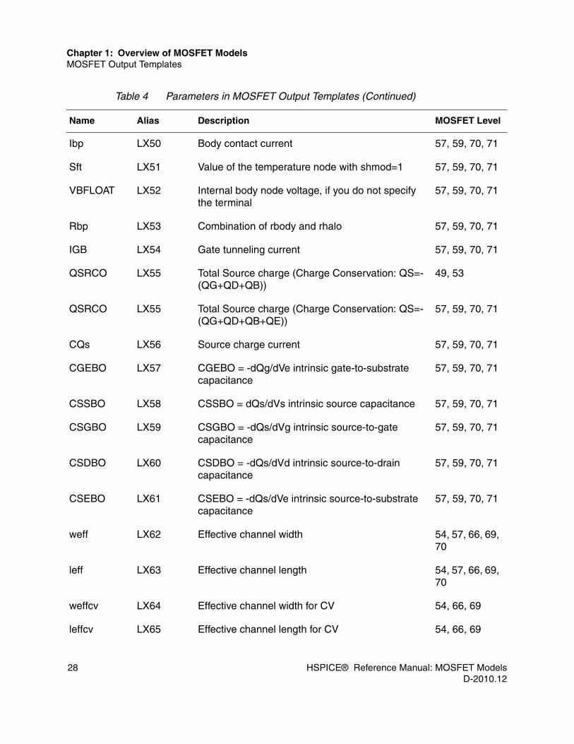
28 HSPICE® Reference Manual: MOSFET ModelsD-2010.12
Chapter 1: Overview of MOSFET ModelsMOSFET Output Templates
Ibp LX50 Body contact current 57, 59, 70, 71
Sft LX51 Value of the temperature node with shmod=1 57, 59, 70, 71
VBFLOAT LX52 Internal body node voltage, if you do not specify the terminal
57, 59, 70, 71
Rbp LX53 Combination of rbody and rhalo 57, 59, 70, 71
IGB LX54 Gate tunneling current 57, 59, 70, 71
QSRCO LX55 Total Source charge (Charge Conservation: QS=-(QG+QD+QB))
49, 53
QSRCO LX55 Total Source charge (Charge Conservation: QS=-(QG+QD+QB+QE))
57, 59, 70, 71
CQs LX56 Source charge current 57, 59, 70, 71
CGEBO LX57 CGEBO = -dQg/dVe intrinsic gate-to-substrate capacitance
57, 59, 70, 71
CSSBO LX58 CSSBO = dQs/dVs intrinsic source capacitance 57, 59, 70, 71
CSGBO LX59 CSGBO = -dQs/dVg intrinsic source-to-gate capacitance
57, 59, 70, 71
CSDBO LX60 CSDBO = -dQs/dVd intrinsic source-to-drain capacitance
57, 59, 70, 71
CSEBO LX61 CSEBO = -dQs/dVe intrinsic source-to-substrate capacitance
57, 59, 70, 71
weff LX62 Effective channel width 54, 57, 66, 69, 70
leff LX63 Effective channel length 54, 57, 66, 69, 70
weffcv LX64 Effective channel width for CV 54, 66, 69
leffcv LX65 Effective channel length for CV 54, 66, 69
Table 4 Parameters in MOSFET Output Templates (Continued)
Name Alias Description MOSFET Level

HSPICE® Reference Manual: MOSFET Models 29D-2010.12
Chapter 1: Overview of MOSFET ModelsMOSFET Output Templates
igbo LX66 Gate-to-Substrate Current (Igb = Igbacc + Igbinv) 54, 69
igcso LX67 Source Partition of Igc 54, 69
igcdo LX68 Drain Partition of Igc 54, 69
iimi LX69 Impact ionization current 54, 69
igidlo LX70 Gate-induced drain leakage current 54, 69
igdt LX71 Gate Dielectric Tunneling Current (Ig = Igs + Igd + Igcs + Igcd + Igb)
54, 69
igc LX72 Gate-to-Channel Current at zero Vds 54, 69
igbacc LX73 Determined by ECB (Electron tunneling from the Conduction Band); significant in the accumulation
54
igbinv LX74 Determined by EVB (Electron tunneling from the Valence Band); significant in the inversion
54
vfbsd LX75 Flat-band Voltage between the Gate and S/D diffusions
54, 66
vgse LX76 Effective Gate-to-Source Voltage 54, 66
vox LX77 Voltage Across Oxide 54, 66
rdv LX78 Asymmetric and Bias-Dependent Source Resistance, (rdsMod = 1)
54, 66
rsv LX79 Asymmetric and Bias-Dependent Drain Resistance, (rdsMod = 1)
54, 66
cap_bsz LX80 Zero voltage bias bulk-source capacitance 54, 66
cap_bdz LX81 Zero voltage bias bulk-drain capacitance 54, 66
CGGBM LX82 Total gate capacitance (including intrinsic), and all overlap and fringing components
54, 57, 59, 60, 66, 70, 69, 71
Table 4 Parameters in MOSFET Output Templates (Continued)
Name Alias Description MOSFET Level

30 HSPICE® Reference Manual: MOSFET ModelsD-2010.12
Chapter 1: Overview of MOSFET ModelsMOSFET Output Templates
CGDBM LX83 Total gate-to-drain capacitance (including intrinsic), and overlap and fringing components
54, 57, 59, 60, 66, 69, 70, 71
CGSBM LX84 Total gate-to-source capacitance (including intrinsic), and overlap and fringing components
54, 57, 59, 60, 66, 69, 70, 71
CDDBM LX85 Total drain capacitance (including intrinsic), overlap and fringing components, and junction capacitance
54, 57, 59, 60, 66, 69, 70, 71
CDSBM LX86 Total drain-to-source capacitance 54, 57, 60, 66, 69, 70, 71
CDGBM LX87 Total drain-to-gate capacitance (including intrinsic), and overlap and fringing components
54, 57, 59, 60, 66, 69, 70, 71
CBGBM LX88 Total bulk-to-gate (floating body-to-gate) capacitance, including intrinsic and overlap components
54, 57, 59, 60, 66, 70, 71
CBDBM LX89 Total bulk-to-drain capacitance (including intrinsic), and junction capacitance
54, 66
CBDBM LX89 Total floating body-to-drain capacitance (including intrinsic), and junction capacitance.
57, 59, 60, 70, 71
CBSBM LX90 Total bulk-to-source capacitance (including intrinsic), and junction capacitance
54, 66
CBSBM LX90 Total floating body-to-source capacitance (including intrinsi)c, and junction capacitance.
57, 59, 60, 70, 71
CAPFG LX91 Fringing capacitance 54, 66
CDEBM LX92 Total drain-to-substrate capacitance (including intrinsi)c, and junction capacitance.
57, 59, 60, 70, 71
CSGBM LX93 Total source-to-gate capacitance (including intrinsic), and overlap and fringing components.
57, 59, 60, 70, 71
Table 4 Parameters in MOSFET Output Templates (Continued)
Name Alias Description MOSFET Level

HSPICE® Reference Manual: MOSFET Models 31D-2010.12
Chapter 1: Overview of MOSFET ModelsMOSFET Output Templates
CSSBM LX94 Total source capacitance (including intrinsic), overlap and fringing components, and junction capacitance.
57, 59, 60, 70, 71
CSEBM LX95 Total source-to-substrate capacitance (including intrinsic), and junction capacitance.
57, 59, 60, 70, 71
CEEBM LX96 Total substrate capacitance (including intrinsic), overlap and fringing components, and junction capacitance.
57, 59, 60, 70, 71
QGI LX97 Intrinsic Gate charge 49, 53
QSI LX98 Intrinsic Source charge 49, 53
QDI LX99 Intrinsic Drain charge 49, 53
QBI LX100 Intrinsic Bulk charge (Charge Conservation: QBI= -(QGI+ QSI+ QDI))
49, 53
CDDBI LX101 Intrinsic drain capacitance; only includes derivative of charge
49, 53
CBDBI LX102 Intrinsic bulk-to-drain capacitance; only includes derivative of charge
49, 53
CBSBI LX103 Intrinsic bulk-to-source capacitance; only includes derivative of charge
49, 53
VBDI LX109 Body-drain voltage(VBD)—Meyer and Charge Conservation
57, 58, 59, 70, 71
IGISLO LX110 Gate-induced source leakage current 54
GRII LX118 Intrinsic channel reflected gate conductance 54
GRGELTD LX119 Gate electrode conductance 54
bs1 LX120 Bulk to source diffusion current 57, 59, 60
Ibd1 LX121 Bulk to drain diffusion current 57, 59, 60
Table 4 Parameters in MOSFET Output Templates (Continued)
Name Alias Description MOSFET Level

32 HSPICE® Reference Manual: MOSFET ModelsD-2010.12
Chapter 1: Overview of MOSFET ModelsMOSFET Output Templates
Ibs2 LX122 Bulk to source recombination/trap-assisted tunneling current
57, 59, 60
Ibd2 LX123 Bulk to drain recombination/trap-assisted tunneling current
57, 59, 60
Ibs3 LX124 Bulk to source recombination current in neutral body
57, 59, 60
Ibd3 LX125 Bulk to drain recombination current in neutral body 57, 59, 60
Ibs4 LX126 Bulk to source reversed bias tunneling leakage current
57, 59, 60
Ibd4 LX127 Bulk to drain reversed bias tunneling leakage current
57, 59, 60
b4_sca LX128 sca for WPE effect 54
b4_scb LX129 scb for WPE effect 54
b4_scc LX130 scc for WPE effect 54
b4_sc LX131 sc for WPE effect 54
Ueff LX132 Effective mobility at the specified analysis temperature
66
VGB LX133 Gate to bulk voltage All
VDG LX134 Drain to gate voltage All
mult LX135 Prints value of multiplier (M) for a specified MOSFET
All
b4_sa LX136 sa for STI or LOD-induced mechanical stress-effects
54
b4_sb LX137 sb for STI or LOD-induced mechanical stress-effects
54
Table 4 Parameters in MOSFET Output Templates (Continued)
Name Alias Description MOSFET Level

HSPICE® Reference Manual: MOSFET Models 33D-2010.12
Chapter 1: Overview of MOSFET ModelsMOSFET Output Templates
Additional MOSFET Output templates include:■ Output Template for Parameters in HiSIM-HVMOS v.1.2.0 and Higher
(level=73)■ New Output Templates for PSP and Other Models
Output Template for Parameters in HiSIM-HVMOS v.1.2.0 and Higher (level=73)HSPICE supports parameter output templates for HiSIM-HV beginning with version 1.2.0 model (version=1.20 level=73).
b4_sd LX138 sd for STI or LOD-induced mechanical stress-effects
54
b4_nf LX139 nf for STI or LOD-induced mechanical stress-effects
54
b4_saeff LX140 saeff for STI or LOD-induced mechanical stress-effects
54
b4_sbeff LX141 sbeff for STI or LOD-induced mechanical stress-effects
54
ivth(m*) LX142 (m*) New vth output, based on the monotony Id/Vgs curve obtained through .OPTION IVTH; ivthn and ivthp support NMOS and PMOS, respectively
54, 69, 70
soiq0 LX143 (bqi)
Initial floating body charge at t=0 for BQI. If it is not given, 1e35 will be printed. For tran analysis (t>0), the floating body charge will be printed. This parameter only supports BQI.
57, 60, 70
Table 5 Output Templates for HiSIM LDMOS/HVMOS Model -1.2.0
Name Alias Description
L LX291 Channel Length (L)
Table 4 Parameters in MOSFET Output Templates (Continued)
Name Alias Description MOSFET Level

34 HSPICE® Reference Manual: MOSFET ModelsD-2010.12
Chapter 1: Overview of MOSFET ModelsMOSFET Output Templates
W LX292 Channel Width (W)
AD LX293 Area of the drain diode (AD)
AS LX294 Area of the source diode (AS)
ICVDS LX295 Initial condition for the drain-source voltage (VDS)
ICVGS LX296 Initial condition for the gate-source voltage (VGS)
ICVBS LX297 Initial condition for the bulk-source voltage (VBS)
PD LX298 Drain diode periphery (PD)
PS LX299 Source diode periphery (PS)
RSS LX301 Source resistance (squares) (RSS)
WEFF LX302 Effective channel width
LEFF LX303 Effective channel length
CAPFG LX304 Fringing capacitance
VTH LX305 Threshold voltage (bias dependent)
VDSAT LX306 Saturation voltage (VDSAT)
GDEFF LX307 Effective drain conductance (1/RDeff)
GSEFF LX308 Effective source conductance (1/RSeff)
VDBEFF LX309 Effective drain bulk voltage.
BETAEFF LX310 BETA effective
GAMMAEFF LX311 GAMMA effective
VFBEFF LX312 VFB effective
COVLGS LX313 Gate-source overlap and fringing capacitances
Table 5 Output Templates for HiSIM LDMOS/HVMOS Model -1.2.0 (Continued)
Name Alias Description

HSPICE® Reference Manual: MOSFET Models 35D-2010.12
Chapter 1: Overview of MOSFET ModelsMOSFET Output Templates
COVLGD LX314 Gate-drain overlap and fringing capacitances
COVLGB LX315 Gate-bulk overlap capacitances
VBD LX316 Bulk-drain voltage
VBS LX317 Bulk-source voltage (VBS)
VGS LX318 Gate-source voltage (VGS)
VDS LX319 Drain-source voltage (VDS)
CDO LX320 Channel current (IDS)
CBSO LX321 DC source-bulk diode current (CBSO)
CBDO LX322 DC drain-bulk diode current (CBDO)
GMO LX323 DC MOSFET gate transconductance (GMO)
GDSO LX324 DC drain-source conductance (GDSO)
GMBSO LX325 DC substrate transconductance (GMBSO)
GBDO LX326 Conductance of the drain diode (GBDO)
GBSO LX327 Conductance of the source diode (GBSO)
QB LX328 Total bulk (body) charge (QB)—Meyer and Charge Conservation
CQB LX329 Bulk (body) charge current (CQB)—Meyer and Charge Conservation
QG LX330 Total Gate charge (QG)—Meyer and Charge Conservation
CQG LX331 Gate charge current (CQG)—Meyer and Charge Conservation
QD LX332 Channel charge (QD)
CQD LX333 Channel charge current (CQD)
CGGBO LX334 Intrinsic gate capacitance
Table 5 Output Templates for HiSIM LDMOS/HVMOS Model -1.2.0 (Continued)
Name Alias Description

36 HSPICE® Reference Manual: MOSFET ModelsD-2010.12
Chapter 1: Overview of MOSFET ModelsMOSFET Output Templates
CGDBO LX335 Intrinsic gate-to-drain capacitance
CGSBO LX336 Intrinsic gate-to-source capacitance
CBGBO LX337 Intrinsic bulk-to-gate capacitance
CBDBO LX338 Intrinsic bulk-to-drain capacitance
CBSBO LX339 CBSBO = -dQb/dVs
QBD LX340 Drain-bulk charge (QBD)
QBS LX341 Source-bulk charge (QBS)
CAP_BS LX342 Bias dependent bulk-source capacitance
CAP_BD LX343 Bias dependent bulk-drain capacitance
CDGBO LX344 Intrinsic drain-to-gate capacitance
CDDBO LX345 Intrinsic drain capacitance
CDSBO LX346 CDSBO = -dQd/dVs, Drain-to-source capacitance
SFT LX347 Value of the temperature node
weffcv LX348 Effective channel width for CV
leffcv LX349 Effective channel length for CV
igso LX350 Gate-to-Source Current
igdo LX351 Gate-to-Drain Current
igbo LX352 Gate-to-Substrate Current
igcso LX353 Source Partition of Igc
igcdo LX354 Drain Partition of Igc
iimi LX355 Impact ionization current
Table 5 Output Templates for HiSIM LDMOS/HVMOS Model -1.2.0 (Continued)
Name Alias Description

HSPICE® Reference Manual: MOSFET Models 37D-2010.12
Chapter 1: Overview of MOSFET ModelsMOSFET Output Templates
igidlo LX356 Gate-induced drain leakage current
igislo LX357 Gate-induced source leakage current
igdt LX358 Gate Dielectric Tunneling Current (Ig = Igs + Igd + Igcs + Igcd + Igb)
vgse LX359 Effective Gate-to-Source Voltage
rdv LX360 Asymmetric and Bias-Dependent Source Resistance
rsv LX361 Asymmetric and Bias-Dependent Drain Resistance
cap_bsz LX362 Zero voltage bias bulk-source capacitance
cap_bdz LX363 Zero voltage bias bulk-drain capacitance
CGGBM LX364 Total gate capacitance (including intrinsic), and overlap and fringing components
CGDBM LX365 Total gate-to-drain capacitance (including intrinsic), and overlap and fringing components
CGSBM LX366 Total gate-to-source capacitance (including intrinsic), and overlap and fringing components
CDDBM LX367 Total drain capacitance (including intrinsic), overlap and fringing components, and junction capacitance
CDSBM LX368 Total drain-to-source capacitance
CDGBM LX369 Total drain-to-gate capacitance (including intrinsic), and overlap and fringing components
CBGBM LX370 Total bulk-to-gate (floating body-to-gate) capacitance, including intrinsic and overlap components
CBDBM LX371 Total bulk-to-drain capacitance (including intrinsic) and junction capacitance
CBSBM LX372 Total bulk-to-source capacitance (including intrinsic), and junction capacitance
Table 5 Output Templates for HiSIM LDMOS/HVMOS Model -1.2.0 (Continued)
Name Alias Description

38 HSPICE® Reference Manual: MOSFET ModelsD-2010.12
Chapter 1: Overview of MOSFET ModelsMOSFET Output Templates
New Output Templates for PSP and Other ModelsThe following output templates do not require an HSPICE alias and are all in support of the PSP model. Note that LPOLY and WPOLY also support BSIM3, BSIM4, BSIM3-SOI, and BSIM4-SOI models.
The output templates of HiSIM-HVMOS (available beginning with version=1.20, level=73) are found in Table 104 on page 327.
Ueff LX373 Effective mobility at the specified analysis temperature
VGB LX374 Gate to bulk voltage
VDG LX375 Drain to gate voltage
mult LX376 Prints value of multiplier (M) for a specified MOSFET
sa LX377 sa for STI or LOD-induced mechanical stress-effects
sb LX378 sb for STI or LOD-induced mechanical stress-effects
sd LX379 sd for STI or LOD-induced mechanical stress-effects
hsmhv_nf LX380 nf for STI or LOD-induced mechanical stress-effects
Table 6 New Output Templates for PSP MOSFETs
Name Description Model Level
LPOY POLY Length 49,53,54,57, 69, 70
WPOLY POLY Width 49,53,54,57,69,70
VFB Flat-band voltage at TR after geometry scaling 69
STVFB Temperature dependence of VFB after geometry scaling 69
TOX Gate oxide thickness after geometry scaling 69
Table 5 Output Templates for HiSIM LDMOS/HVMOS Model -1.2.0 (Continued)
Name Alias Description

HSPICE® Reference Manual: MOSFET Models 39D-2010.12
Chapter 1: Overview of MOSFET ModelsMOSFET Output Templates
EPSROX Relative permittivity of gate dielectric)after geometry scaling 69
NEFF Substrate doping after geometry scaling 69
VNSUB Effective doping bias-dependence parameter)after geometry scaling
69
NSLP Effective doping bias-dependence parameter after geometry scaling
69
DNSUB Effective doping bias-dependence parameter after geometry scaling
69
DPHIB Offset of ) after geometry scaling 69
NP NP Gate poly-silicon doping after geometry scaling 69
CT Interface states factor after geometry scaling 69
TOXOV Overlap oxide thickness after geometry scaling 69
NOV Effective doping of overlap region after geometry scaling 69
CF DIBL parameter after geometry scaling 69
CFB Back-bias dependence of CF after geometry scaling 69
BETN Product of channel aspect ratio and zero field mobility at TR after geometry scaling
69
STBET Temperature dependence of BETN after geometry scaling 69
MUE Mobility reduction coefficient at TR after geometry scaling 69
STMUE Temperature dependence of MUE after geometry scaling 69
THEMU Mobility reduction exponent at TR after geometry scaling 69
STTHEMU Temperature dependence of THEMU after geometry scaling 69
CS Coulomb scattering parameter at TR after geometry scaling 69
Table 6 New Output Templates for PSP MOSFETs (Continued)
Name Description Model Level
ϕB

40 HSPICE® Reference Manual: MOSFET ModelsD-2010.12
Chapter 1: Overview of MOSFET ModelsMOSFET Output Templates
STCS Temperature dependence of CS after geometry scaling 69
XCOR Non-universality parameter after geometry scaling 69
STXCOR Temperature dependence of XCOR after geometry scaling 69
FETA Effective field parameter after geometry scaling 69
RS Source/drain series resistance at TR after geometry scaling 69
STRS Temperature dependence of RS after geometry scaling 69
RSB Back-bias dependence of RS after geometry scaling 69
RSG Gate-bias dependence of RS) after geometry scaling 69
THESAT Velocity saturation parameter at TR after geometry scaling 69
STTHESAT Temperature dependence of THESAT after geometry scaling 69
THESATB Back-bias dependence of velocity saturation after geometry scaling 69
THESATG Gate-bias dependence of velocity saturation) after geometry scaling
69
AX Linear/saturation transition factor after geometry scaling 69
ALP CLM pre-factor after geometry scaling 69
ALP1 CLM enhancement factor above threshold) after geometry scaling 69
ALP2 CLM enhancement factor below threshold) after geometry scaling 69
VPO CLM logarithmic dependence parameter) after geometry scaling 69
A1 Impact-ionization pre-factor after geometry scaling 69
A2 Impact-ionization exponent at TR after geometry scaling 69
STA2 Temperature dependence of A2 after geometry scaling 69
A3 Saturation-voltage dependence of II after geometry scaling 69
Table 6 New Output Templates for PSP MOSFETs (Continued)
Name Description Model Level
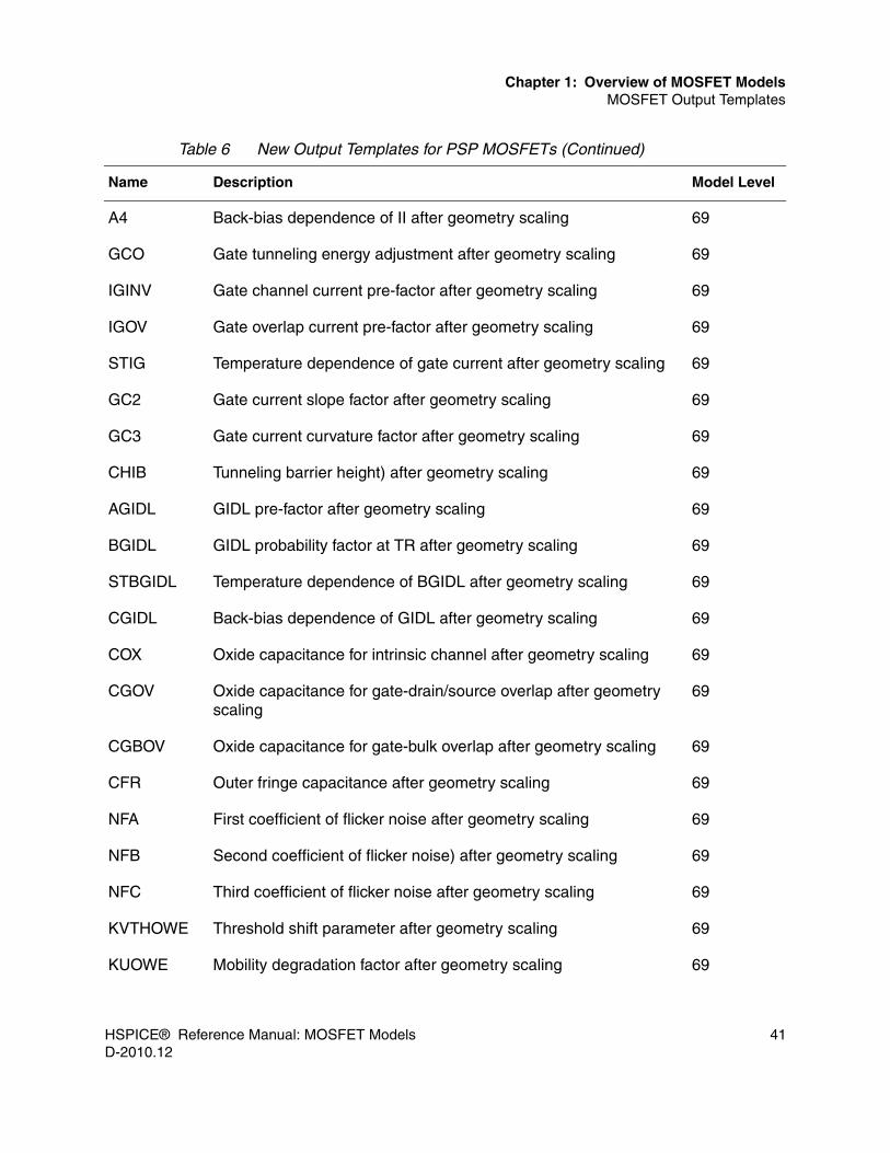
HSPICE® Reference Manual: MOSFET Models 41D-2010.12
Chapter 1: Overview of MOSFET ModelsMOSFET Output Templates
A4 Back-bias dependence of II after geometry scaling 69
GCO Gate tunneling energy adjustment after geometry scaling 69
IGINV Gate channel current pre-factor after geometry scaling 69
IGOV Gate overlap current pre-factor after geometry scaling 69
STIG Temperature dependence of gate current after geometry scaling 69
GC2 Gate current slope factor after geometry scaling 69
GC3 Gate current curvature factor after geometry scaling 69
CHIB Tunneling barrier height) after geometry scaling 69
AGIDL GIDL pre-factor after geometry scaling 69
BGIDL GIDL probability factor at TR after geometry scaling 69
STBGIDL Temperature dependence of BGIDL after geometry scaling 69
CGIDL Back-bias dependence of GIDL after geometry scaling 69
COX Oxide capacitance for intrinsic channel after geometry scaling 69
CGOV Oxide capacitance for gate-drain/source overlap after geometry scaling
69
CGBOV Oxide capacitance for gate-bulk overlap after geometry scaling 69
CFR Outer fringe capacitance after geometry scaling 69
NFA First coefficient of flicker noise after geometry scaling 69
NFB Second coefficient of flicker noise) after geometry scaling 69
NFC Third coefficient of flicker noise after geometry scaling 69
KVTHOWE Threshold shift parameter after geometry scaling 69
KUOWE Mobility degradation factor after geometry scaling 69
Table 6 New Output Templates for PSP MOSFETs (Continued)
Name Description Model Level

42 HSPICE® Reference Manual: MOSFET ModelsD-2010.12
Chapter 1: Overview of MOSFET ModelsMOSFET Output Templates
TOXOVD Overlap oxide thickness for drain side after geometry scaling 69
NOVD Effective doping of overlap region for drain side after geometry scaling
69
IGOVD Gate overlap current pre-factor for drain side after geometry scaling 69
AGIDLD GIDL pre-factor for drain side after geometry scaling 69
BGIDLD GIDL probability factor at TR for drain side after geometry scaling 69
STBGIDLD Temperature dependence of BGIDL for drain side after geometry scaling
69
CGIDLD Back-bias dependence of GIDL for drain side after geometry scaling
69
CGOVD Oxide capacitance for gate-drain/source overlap for drain side after geometry scaling
69
CFRD Outer fringe capacitance for drain side after geometry scaling 69
EF Flicker noise frequency exponent after geometry scaling 69
FACNEFFAC Pre-factor for effective substrate doping in separate charge calculation when SWDELVTAC = 1 after geometry scaling
69
GFACNUD Body factor change due to NUD-effect after geometry scaling 69
VSBNUD Lower VSB-value for NUD-effect after geometry scaling 69
DVSBNUD VSB-range for NUD-effect after geometry scaling 69
DELVTAC Offset of in separate charge calculation when SWDELVTAC=1 after geometry scaling
69
MOBEFF Effective mobility at the specified analysis temperature. Note: For PSP, the effective mobility calculation considers geometry and temperature scaling, plus mechanical stress and electrical field-induced mobility change.
54, 69, 70
Table 6 New Output Templates for PSP MOSFETs (Continued)
Name Description Model Level
ϕB

HSPICE® Reference Manual: MOSFET Models 43D-2010.12
Chapter 1: Overview of MOSFET ModelsSafe Operating Area Voltage Warning
Safe Operating Area Voltage Warning
The following warning message is issued when terminal voltages of a device (MOSFET, BJT, Diode, Resistor, Capacitor, etc.) exceed their safe operating area (SOA):
**warning**(filename:line number) resulted during SOA check <node voltage name> (=val) of <device/element name> has exceeded <node voltage name>_max (=val)
To turn it off use .option WARN=0
Example Warnings**Warning**(res1 : r1): Vr = 1.00 has exceeded Bv_max = 0.900**Warning**(cap1 : c1): Vr = 1.00 has exceeded Bv_max = 0.900**Warning**(dio1 : d1): Vr = 1.00 has exceeded Bv_max = 0.900**Warning**(bjt1: q_gp1):Vbe = 1.00 has exceeded Vbe_max = 0.800**Warning**(mos49 : m1): Vgs = 1.00 has exceeded Vgs_max = 0.900**Warning**(mos49 : m1): Vgb = 1.00 has exceeded Vgs_max = 0.900**Warning**(mos49 : m1): Vds = 1.00 has exceeded Vds_max = 0.900**Warning**(mos49 : m1): Vbd = -1.00 has exceeded Vbd_max = 0.900
See the following control options for details:■ .OPTION WARN■ .OPTION MAXWARNS
For details on the the warnings issued, see Safe Operating Area (SOA) Warnings in the HSPICE User Guide: Simulation and Analysis.
Model Pre-Processing and Parameter Flattening
You can invoke model pre-processing and parameter flattening by using .OPTION MODPRT=1. For details, see .OPTION MOD PRT in the HSPICE Reference Manual: Commands and Control Options.
Use of Example Syntax
To copy and paste proven syntax use the demonstration files shipped with your installation of HSPICE (see Listing of Demonstration Input Files). Attempting to

44 HSPICE® Reference Manual: MOSFET ModelsD-2010.12
Chapter 1: Overview of MOSFET ModelsUse of Example Syntax
copy and paste from the book or help documentation may present unexpected results, as text used in formatting may include hidden characters, white space, etc. for visual clarity.

HSPICE® Reference Manual: MOSFET Models 45D-2010.12
2
2Common MOSFET Model Parameters
Lists and describes parameters that are common to several or all MOSFET model levels.
HSPICE ships hundreds of examples for your use; see Listing of Demonstration Input Files for paths to demo files.
Parameters that are unique to a specific MOSFET model level are described in later chapters, as part of the description of the specific model level that uses the parameter.
The common MOSFET parameters are presented in the following sections:■ Basic MOSFET Model Parameters■ Effective Width and Length Parameters ■ Threshold Voltage Parameters■ Mobility Parameters
Note: MOSFET LEVELs 4 through 8 are not supported in HSPICE RF.

46 HSPICE® Reference Manual: MOSFET ModelsD-2010.12
Chapter 2: Common MOSFET Model ParametersBasic MOSFET Model Parameters
Basic MOSFET Model Parameters
Table 7 lists the basic MOSFET model parameters.
Table 7 Basic MOSFET Model Parameters
Name (Alias) Units Default Description Level
LEVEL 1.0 DC model selector:■ LEVEL=1 (default) is the Schichman-
Hodges model.■ LEVEL=2 is the Grove-Frohman model.■ LEVEL=3 is an empirical model.■ LEVEL=4 is a modified version of Level
2.■ LEVEL=5 is the IDS model with
enhancement and depletion modes.■ LEVEL=6 is the Lattin-Jenkins-Grove
model us using ASPEC-style parasitics.■ LEVEL=7 is the Lattin-Jenkins-Grove
model us using SPICE-style parasitics.■ LEVEL=8 is an advanced model using
finite differences.■ LEVEL=13 is the University of California
(UC) Berkeley BSIM1 model.■ LEVEL=27 is the SOSFET model.■ LEVEL=28 is a Synopsys proprietary
model, based on the UC Berkeley BSIM1 model, Level 13.
■ LEVEL=38 is the Cypress Depletion model.
■ LEVEL=39 is the UC Berkeley BSIM2 model.
■ LEVEL=40 is the Hewlett-Packard amorphous-silicon Then-Film Transistor (a-Si TFT) model.
■ LEVEL=47 is the UC Berkeley BSIM3 version 2 model
■ LEVEL=49 is a Synopsys proprietary model, based on the UC Berkeley BSIM3 version 3 model, Level 53.
All

HSPICE® Reference Manual: MOSFET Models 47D-2010.12
Chapter 2: Common MOSFET Model ParametersBasic MOSFET Model Parameters
LEVEL (continued)
■ LEVEL=50 is the Philips MOS9 model.■ LEVEL=53 is the original UC Berkeley
BSIM3 version 3 model, not modified as Level 49 is.
■ LEVEL=54 is the UC Berkeley BSIM4 model
■ LEVEL=55 is the EPFL-EKV model.■ LEVEL=57 is the UC Berkeley BSIM3-
SOI Partially-Depleted (PD) model.■ LEVEL=58 is the University of Florida
SOI model■ LEVEL=59 is the UC Berkeley BSIM3-
SOI Fully-Depleted (FD) model■ LEVEL=60 is the UC Berkeley BSIM3-
SOI Dynamically-Depleted (DD) model■ LEVEL=61 is the Rensselaer
Polytechnic Institute (RPI) a-Si TFT model
■ LEVEL=62 is the Rensselaer Polytechnic Institute (RPI) poly-silicon Thin-Film Transistor (Poli-Si TFT) model
■ LEVEL=63 is the Philips MOS11 model■ LEVEL=64 is the Hiroshima University
Semiconductor Technology Academic Research Center (STARC) IGFET (HiSIM) model.
■ LEVEL=69 is Pennsylvania State University and Philips Research PSP100 model
All
ACM - 0 Selects MOS S/D parasitics. ACM=0 is SPICE style. Use ACM=2 or 3 for LDD.
39
ALPHA V-1 0 Impact ionization coefficient. This parameter includes geometry-sensitivity parameters. Choose between BSIM2 (A10>0 and HSPICE (ALPHA>0) impact ionization modeling. Do not use both.
39
Table 7 Basic MOSFET Model Parameters
Name (Alias) Units Default Description Level

48 HSPICE® Reference Manual: MOSFET ModelsD-2010.12
Chapter 2: Common MOSFET Model ParametersBasic MOSFET Model Parameters
CAPOP - * MOS gate cap model selector: CAPOP=39 for BSIM2 or CAPOP=13 for BSIM1. CAPOP=4 is the same as CAPOP=13. ■ If SPICE3=0, default CAPOP=13■ If SPICE3=1, default CAPOP=39
4, 13 39
CGBO F/m - Gate-to-bulk overlap capacitance.
If you specify WD and TOX, but you do not specify CGBO, then simulation calculates CGBO.
39
CGDO F 1.0p TFT gate-to-drain overlap capacitance. 40
F/m - Gate-to-drain overlap capacitance.
If you specify TOX, and you specify either LD or METO, but you do not specify CGDO, then simulation calculates CGDO.
39
CGSO F 1.0p TFT gate-to-source overlap capacitance. 40
F/m - Gate-to-source overlap capacitance.
If you specify TOX, but you do not specify either LD or METO, and you do not specify CGSO, then simulation calculates CGSO.
39
CHI 0.5 Temperature exponential part. 40
CJ F/m2 0 Source/drain bulk zero-bias junction capacitance.
39
CJSW F/m 0 Sidewall junction capacitance. 39
CLM (GDS) 0.0 Selects a channel length modulation equation.
6, 7, 8
Table 7 Basic MOSFET Model Parameters
Name (Alias) Units Default Description Level

HSPICE® Reference Manual: MOSFET Models 49D-2010.12
Chapter 2: Common MOSFET Model ParametersBasic MOSFET Model Parameters
COX F/m2 3.453e-4 Oxide capacitance per unit gate area. If you do not specify COX, simulation calculates it from TOX.
1, 2, 3, 8
CSC F/m2 10μ Space charge capacitance. 40
DEFF 2.0 Drain voltage effect for the TFT leakage current.
40
DERIV 1 Derivative method selector:■ DERIV=0: analytic■ DERIV=1: finite difference
3, 39
DP μm 1.0 Implant depth (depletion model only). 5, 38
ECRIT (ESAT)
V/cm 0.0 Critical electric field for the carrier velocity saturation. From Grove: ■ electrons 6e4■ holes 2.4e4.
Zero indicates an infinite value. The ECRIT equation is more stable than VMAX. Simulation estimates ECRIT as:
ECRIT=100 ⋅ (VMAX / UO)
2, 8
V/cm 0.0 Drain-source critical field. Zero indicates an infinite value, typically 40,000 V/cm.
6, 7
ECV V/μm 1000 Critical field. 5, 38
FEFF 0.5 Frequency effect constant. 40
FREQ Hz 400 Frequency of the device. 40
GO ohm-1 10e-15 Conductance of the TFT leakage current. 40
Table 7 Basic MOSFET Model Parameters
Name (Alias) Units Default Description Level

50 HSPICE® Reference Manual: MOSFET ModelsD-2010.12
Chapter 2: Common MOSFET Model ParametersBasic MOSFET Model Parameters
IIRAT - 0 Impact ionization source bulk current partitioning factor. One corresponds to 100% source. Zero corresponds to 100% bulk.
39
JS A/m2 0 Source/drain bulk diode reverse saturation current density.
39
K2 2.0 Temperature exponential part. 40
KAPPA V-1 0.2 Saturation field factor. The channel length modulation equation uses this parameter.
3
KCS 2.77 Implant capacitance integration constant. 38
KP (BET, BETA)
A/V2 Intrinsic transconductance parameter. If you specify U0 and TOX, but you do not specify KP, simulation computes the parameter from:
KP=UO ⋅ COX. ■ Level 1 default=2.0718e-5 (NMOS),
8.632e-6 (PMOS).■ Level 2, 3 default=2.0e-5
1, 2, 3
LAMBDA (LAM, LA)
V-1 0.0 Channel length modulation. 2, 8
MJ - 0.5 Source/drain bulk junction grading coefficient.
39
MJSW 0.33 Sidewall junction grading coefficient. 39
NEFF 1.0 Total channel charge (fixed and mobile) coefficient.
2
NI cm-2 2e11 Implant doping (depletion model only). 5, 38
NU 0.0 First order temperature gradient. 40
PB V 0.8 Source/drain bulk junction potential. 39
Table 7 Basic MOSFET Model Parameters
Name (Alias) Units Default Description Level

HSPICE® Reference Manual: MOSFET Models 51D-2010.12
Chapter 2: Common MOSFET Model ParametersBasic MOSFET Model Parameters
PBSW V PB Sidewall junction potential. 39
PSI 1e-20 Temperature exponential part. 40
RD ohm 1.0K (External) drain resistance. 40
RS ohm 1.0K (External) source resistance. 40
RSH ohm/sq 0 Source/drain sheet resistance. 39
SNVB 1/(V⋅ cm3) 0.0 Slope of the doping concentration versus vsb (element parameter). (Multiplied by 1e6).
8
SPICE3 - 0 Selects SPICE3 model compatibility. For accurate SPICE3 BSIM2, set SPICE3=1.
39
TAU s 10n Relaxation time constant. 40
TCV V/C 0 Zero-bias threshold voltage temperature coefficient. The sign of TCV adjusts automatically for NMOS and PMOS to decrease the magnitude of the threshold with rising temperature.
39
TOX m 1e-7 Gate oxide thickness. 1, 2, 3, 8
Å 0.0 Oxide thickness. 5, 38
m 7.0e-8 Oxide thickness. 27
TRD 1/K 0.0 Temperature coefficient for the Rd drain diffusion and contact resistances.
54
TREF 1.5 Temperature gradient of UO. 40
TRS 1/K 0.0 Temperature coefficient for the Rs source diffusion and contact resistances.
54
Table 7 Basic MOSFET Model Parameters
Name (Alias) Units Default Description Level

52 HSPICE® Reference Manual: MOSFET ModelsD-2010.12
Chapter 2: Common MOSFET Model ParametersBasic MOSFET Model Parameters
TUH 1.5 Implant channel mobility temperature exponent (depletion model only).
5
UO cm2/(V⋅ s) Carrier mobility.
Default for LEVEL 40 is 1.0.
1, 40
UO (UB, UBO)
cm2/(V·s) 600 (N)250 (P)
Low-field bulk mobility.Simulation calculates this parameter from the KP value that you specify.
2
VB0 (VB) V 0.0 Reference voltage for the GAMMA switch. ■ If vsb < VB0, the equation uses
GAMMA. ■ If vsb > VB0, the equation uses
LGAMMA.
6, 7
VCR V 0 Impact ionization critical voltage. This parameter includes geometry-sensitivity parameters.
39
VMAX (VMX, VSAT)
m/s 0.0 Maximum drift velocity of the carriers. Zero indicates an infinite value.Default VMAX value for Level 40 is 1e6.
2, 3, 8, 40
VMAX (VMX) cm/s 0.0 Maximum drift velocity of the carriers. Selects a calculation scheme to use for vdsat. Zero indicates an infinite value. Typical values:■ electrons8.4e6 cm/s ■ holes4.3e6 cm/s
6, 7
VTIME s 10m Voltage stress. 40
ZENH 1.0 Mode flag (enhancement). Set ZENH=0.0 for the depletion mode.
5
Table 7 Basic MOSFET Model Parameters
Name (Alias) Units Default Description Level

HSPICE® Reference Manual: MOSFET Models 53D-2010.12
Chapter 2: Common MOSFET Model ParametersEffective Width and Length Parameters
Effective Width and Length Parameters
Table 8 lists effective width and length parameters.
Table 8 Effective Width and Length Parameters
Name (Alias) Units Default Description Level
DEL m 0.0 Channel length reduction on each side:
DELscaled=DEL ⋅ SCALM
MOSFET Level 13 does not support DEL.
1, 2, 3, 6, 7, 8, 38
DEL (WDEL) μm 0.0 Channel length reduction on each side 5
DELVTO V 0 Threshold voltage shift. This parameter is type sensitive. For example, DELVTO>0 increases the magnitude of the n-channel threshold, decreases the magnitude of the p-channel threshold, and adds to the element-line DELVTO parameter.
39
LATD (LD) μm 1.7 ⋅ XJ Lateral diffusion on each side 5, 38
LDAC m This parameter is the same as LD, but if you specify LDAC in the .MODEL statement, it replaces LD in the Leff calculation for the AC gate capacitance.
1, 2, 3, 6, 7, 8, 13, 28, 38, 39
LMLT 1.0 Gate length shrink factor. 1, 2, 3, 5, 6, 7, 8, 13, 28, 38, 39
Scale MOSFET drawn length 54

54 HSPICE® Reference Manual: MOSFET ModelsD-2010.12
Chapter 2: Common MOSFET Model ParametersEffective Width and Length Parameters
LD (DLAT, LATD)
m Lateral diffusion into the channel from the source and the drain diffusion.■ If you do not specify LD and XJ:
LD Default=0.0■ If you specify XJ, but you do not specify LD,
simulation calculates LD as: LD default=0.75 ⋅ XJ LDscaled=LD ⋅ SCALM
1, 2, 3, 6, 7, 8, 13, 28
LD m 0 Lateral diffusion under the gate (per side) of the S/D junction. Use this parameter to calculate Leff only if DL=0:
LDscaled=LD ⋅ SCALM
39
LREF m 0.0 Channel length reference:
LREFscaled=LREF ⋅ SCALM
If the Level 13 model does not define LREF and WREF, their value is infinity.
2, 3, 6, 7, 8, 13, 28
m 0 ( ) Reference channel length to adjust the length of the BSIM model parameters. For Berkeley compatibility (LREF-> ), use: LREF=0. LREFscaled=LREF ⋅ SCALM
39
OXETCH μm 0.0 Oxide etch 5, 38
Px [x]⋅ μμ2 0 Px is a Synopsys proprietary, WL-product sensitivity parameter, where x is a model parameter with length and width sensitivity.
39
WD m 0.0 Lateral diffusion into the channel from the bulk along the width:
WDscaled=WD ⋅ SCALM
1, 2, 3, 6, 7, 8, 13
Table 8 Effective Width and Length Parameters
Name (Alias) Units Default Description Level
∞
∞

HSPICE® Reference Manual: MOSFET Models 55D-2010.12
Chapter 2: Common MOSFET Model ParametersEffective Width and Length Parameters
m 0 Channel stop lateral diffusion under the gate (per side). Use this parameter to calculate Weff only if DW=0.
WD scaled=WD ⋅ SCALM
39
WDAC m This parameter is the same as WD, but if you specify WDAC in the .MODEL statement, it replaces WD in the Weff calculation for the AC gate capacitance.
1, 2, 3, 6, 7, 8, 13, 28, 39
WMLT 1.0 Diffusion layer and width shrink factor. 1, 2, 3, 5, 6, 7, 8, 13, 28, 38, 54
- 1.0 Diffusion and gate width shrink factor. 39
Scale MOSFET drawn width 54
WREF m 0.0 Channel width reference:
WREFscaled=WREF ⋅ SCALM
If the Level 13 model does not define LREF and WREF, their value is infinity.
2, 3, 6, 7, 8, 13, 28
m 0 ( ) Reference device width to adjust the width of the BSIM model parameters. For Berkeley compatibility (WREF-> ), use WREF=0: WREFscaled=WREF ⋅ SCALM
39
XJ m 0.0 Metallurgical junction depth:
XJscaled=XJ ⋅ SCALM
1, 2, 3, 6, 7, 8
μm 1.5 Junction depth 5, 38
Table 8 Effective Width and Length Parameters
Name (Alias) Units Default Description Level
∞
∞

56 HSPICE® Reference Manual: MOSFET ModelsD-2010.12
Chapter 2: Common MOSFET Model ParametersEffective Width and Length Parameters
XL (DL, LDEL)
m 0.0 Length bias accounts for the masking and etching effects (length):
XLscaled=XL ⋅ SCALM
1, 2, 3, 6, 7, 8, 13, 28, 39
XL m 0 Difference between the physical (on the wafer) and the drawn reference channel length. Use this parameter to calculate Leff only if DL=0:
XLscaled=XL ⋅ SCALMNote: SCALM is ignored for Level 54.
39, 54
XLREF m 0.0 Difference between the physical (on the wafer) and the drawn reference channel length:
XLREFscaled=XLREF ⋅ SCALM
28, 39
XW (DW, WDEL)
m 0.0 Width bias accounts for the masking and etching effects (width):
XWscaled=XW ⋅ SCALM
1, 2, 3, 6, 7, 8, 13, 28
XW m 0 Difference between the physical (on the wafer) and the drawn S/D active width. Use this parameter to calculate Weff only if DW=0: XWscaled=XW ⋅ SCALMNote: SCALM is ignored for Level 54.
39, 54
XWREF m 0.0 Difference between the physical (on the wafer) and the drawn reference channel width:
XWREFscaled=XWREF ⋅ SCALM
28, 39
Table 8 Effective Width and Length Parameters
Name (Alias) Units Default Description Level

HSPICE® Reference Manual: MOSFET Models 57D-2010.12
Chapter 2: Common MOSFET Model ParametersThreshold Voltage Parameters
Threshold Voltage Parameters
Table 9 lists threshold voltage parameters.
Table 9 Threshold Voltage Parameters
Name (Alias)Units Default Description Level
BetaGam 1.0 Body effect transition ratio. 38
CAV 0.0 Thermal voltage multiplier for the weak inversion equation.
8
DELTA 0.0 Narrow width factor for adjusting the threshold.
2, 3, 8
DNB (NSUB) cm-3 0.0 Surface doping density. 5, 38
1/cm3 1.0e15 Substrate doping. 6, 7
DNS (NI) 1/cm3 0.0 Surface substrate doping. 6, 7
DVIN V 0.0 Adjusts the empirical surface inversion voltage.
38
DVSBC V 0.0 Adjusts the empirical body effect transition voltage.
38
E1 3.9 Dielectric constant of first film. 40
E2 0.0 Dielectric constant of second film. 40
ETA V-1
(Level 40)
0.0 Static feedback factor for adjusting the threshold voltage (difficulty of band bending).
3, 40
0.0 Drain-induced barrier lowering (DIBL) effect coefficient for the threshold voltage.
8
0.0 Channel-length independent drain-induced barrier lowering.
38

58 HSPICE® Reference Manual: MOSFET ModelsD-2010.12
Chapter 2: Common MOSFET Model ParametersThreshold Voltage Parameters
FDS 0.0 Field, drain to source. Controls the threshold reduction due to the source-drain electric field.
6, 7
FSS (NFS) cm-2⋅ V-1 0.0 Number of fast surface states 5, 38
GAMMA V1/2 0.5276 Body effect factor. If you do not specify GAMMA, simulation calculates it from NSUB.
1, 2, 3, 8
V1/2 Body effect factor. ■ If you do not specify GAMMA, simulation
calculates it from DNB.■ GAMMA is the body effect, if vsb < VB0.■ If vsb > VB0, simulation uses LGAMMA.
GAMMA, LGAMMA, and VB0 perform a two-step approximation of a non-homogeneous substrate.
6, 7
LBetaGam. μm 0.0 BetaGam dependence on the channel length.
38
LDVSBC V⋅ μm 0.0 Adjusts the L-dependent body effect transition voltage.
38
LETA(DIBL) μm 0.0 Channel-length dependent drain-induced barrier lowering.
38
LGAMMA V1/2 0.0 This parameter is the body effect factor if vsb > VB0.
If you use the Poon-Yau GAMMA expression, LGAMMA is the junction depth in microns. Simulation multiplies LGAMMA by SCALM.
6, 7
LND μm/V 0.0 ND length sensitivity. 2, 3, 6, 7, 8
Table 9 Threshold Voltage Parameters
Name (Alias)Units Default Description Level

HSPICE® Reference Manual: MOSFET Models 59D-2010.12
Chapter 2: Common MOSFET Model ParametersThreshold Voltage Parameters
LN0 μm 0.0 N0 length sensitivity. 2, 3, 6, 7, 8
LVT (LVTO) V⋅ μm 0.0 VT dependence on the channel length. 38
ND V-1
(1/V)
0.0 Drain subthreshold factor. Typical value=1. 2, 3, 6, 7, 8
N0 0.0 Gate subthreshold factor. Typical value=1. 2, 3, 6, 7, 8
NFS (DFS, NF, DNF)
cm-2⋅ V-1 0.0 Fast surface state density. 1, 2, 3, 6, 7, 8
NFS cm2 0.0 Fast surface state density. 40
NSS cm2 0.0 Surface state density. 40
NSUB (DNB, NB)
cm-3 1e15 Bulk surface doping. If you do not specify NSUB, simulation calculates it from GAMMA.
1, 2, 3, 8
NWE m 0.0 Narrow width effect, direct compensation of VTO: NWEscaled=NWE ⋅ SCALM
6, 7
NWM 0.0 Narrow width modifier. 5, 38
0.0 Narrow width modulation of GAMMA. 6, 7
PHI V 0.576 Surface inversion potential. If you do not specify PHI, HSPICE calculates it from NSUB.
1, 2, 3, 8
V 0.8 Built-in potential. 5, 38
V 0.0 Surface potential. 40
SCM 0.0 Short-channel drain source voltage multiplier 5, 38
0.0 Short-channel modulation of GAMMA. 6, 7
Table 9 Threshold Voltage Parameters
Name (Alias)Units Default Description Level

60 HSPICE® Reference Manual: MOSFET ModelsD-2010.12
Chapter 2: Common MOSFET Model ParametersThreshold Voltage Parameters
T1 m 280n First thin film thickness. 40
T2 m 0.0 Second thin film thickness. 40
TDVSBC V/K 0.0 Body effect transition voltage shift due to the temperature.
38
UFDS 0.0 High field FDS. 6, 7
UPDATE 0.0 Selects different versions of the LEVEL 6 model. For the UPDATE=1 or 2 alternate saturation voltage, simulation modifies the MOB=3 mobility equation and the RS and RD series resistances so they are compatible with ASPEC. UPDATE=1 is a continuous Multi-Level GAMMA model.
6, 7
VFDS V 0.0 Reference voltage for selecting FDS or UFDS:■ Uses FDS if vds ≤ VFDS.■ Uses UFDS if vds > VFDS.
6, 7
VSH V 0.0 Threshold voltage shifter for reducing the zero-bias threshold voltage (VTO) as a function of the ratio of LD to Leff.
6, 7
VT (VTO) V 0.0 Extrapolated threshold voltage 5, 38
VTO (VT) V 0.0 Zero-bias threshold voltage. If you do not specify VTO, simulation calculates it.
1, 2, 3, 6, 7, 8, 40
WBetaGam μm 0.0 BetaGam dependence on the channel width. 38
WDVSBC V⋅ μm 0.0 Adjusts the W-dependent body effect transition voltage.
38
WETA μm 0.0 Channel-width dependent drain-induced barrier lowering.
38
Table 9 Threshold Voltage Parameters
Name (Alias)Units Default Description Level

HSPICE® Reference Manual: MOSFET Models 61D-2010.12
Chapter 2: Common MOSFET Model ParametersMobility Parameters
Mobility Parameters
Use curve fitting to determine the mobility parameters. Generally, you should set UTRA between 0.0 and 0.5. Nonzero values for UTRA can result in negative resistance regions at the onset of saturation.
Table 10 lists mobility parameters.
WEX Weak inversion exponent. 6, 7
WIC 0.0 Subthreshold model selector. 2, 3, 6, 7, 8
WND μm/V 0.0 ND width sensitivity. 2, 3, 6, 7, 8
WN0 μm 0.0 N0 width sensitivity. 2, 3, 6, 7
WVT (WVTO)
V⋅ μm 0.0 VT dependence on the channel width. 38
Table 10 Mobility Parameters
Name (Alias) Units Default Description Level
BEX - -1.5 Surface channel mobility temperature exponent.
38, 39
BFRC Å⋅ s/(cm2⋅ V) 0.0 Field reduction coefficient variation due to the substrate bias.
38
FACTOR Mobility degradation factor. Default=1.0.
6, 7
FEX - 0 Temperature exponent for velocity saturation.
39
Table 9 Threshold Voltage Parameters
Name (Alias)Units Default Description Level

62 HSPICE® Reference Manual: MOSFET ModelsD-2010.12
Chapter 2: Common MOSFET Model ParametersMobility Parameters
FRC Å⋅ s/cm2 0.0 Field reduction coefficient. 5, 38
FRCEX(F1EX)
0.0 Temperature coefficient for
FRC
.
38
FSB V1/2⋅ s/cm2 0.0 Lateral mobility coefficient. 5, 38
HEX(TUH) -1.5 Implant channel mobility temperature exponent.
38
KBeta1 1.0 Effective implant-channel mobility modifier.
38
KI0(KIO) 1.0 Residue current coefficient. 38
LBFRC 10-4Å⋅ s/(cm⋅ V) 0.0 BFRC sensitivity to the effective channel length.
38
LFRC 10-4Å⋅ s/cm 0.0 FRC sensitivity to the effective channel length.
38
LKBeta1 μm 0.0 Length-dependent implant-channel mobility modifier.
38
LKI0(LKIO) μm 0.0 Length-dependent residue current coefficient.
38
LUO(LUB) cm2⋅ μm/(V⋅ s) 0.0 UO sensitivity to the effective channel length.
38
LVFRC 10-4Å⋅ s/(cm⋅ V) 0.0 VFRC sensitivity to the effective channel length.
38
LFSB 10-4V1/2 ⋅ s/cm 0.0 FSB sensitivity to the effective channel length.
38
Table 10 Mobility Parameters
Name (Alias) Units Default Description Level

HSPICE® Reference Manual: MOSFET Models 63D-2010.12
Chapter 2: Common MOSFET Model ParametersMobility Parameters
MOB 0.0 Selects a mobility equation. You can set this parameter to MOB=0 or MOB=7. MOB=7 changes both the model and the channel length calculation.
The MOB=7 flag invokes the channel length modulation and mobility equations in MOSFET LEVEL 3.
In MOSFET Level 8, you can set MOB to 2, 3, 6, or 7.
2, 6, 7, 8
THETA V-1 0.0 Mobility modulation. MOSFET models use THETA only if MOB=7. A typical value is THETA=5e-2.
2, 40
V-1 0.0 Mobility degradation factor. 3
UB (UO) cm2/(V⋅ s) 0.0 Low field bulk mobility 5
UCRIT V/cm 1.0e4 Critical field for mobility degradation, UCRIT. This parameter is the limit where UO surface mobility begins to decrease as specified in the empirical relation.
2
V/cm 1e4 ■ MOB=6, UEXP>0 Critical field for the mobility degradation. UEXP operates as a switch.
■ MOB=6, UEXP≤0Critical field for mobility degradation. Typical value is
0.01 V-1.
8
Table 10 Mobility Parameters
Name (Alias) Units Default Description Level

64 HSPICE® Reference Manual: MOSFET ModelsD-2010.12
Chapter 2: Common MOSFET Model ParametersMobility Parameters
UEFF Effective mobility at the specified analysis temperature.
6, 7
UEXP (F2) 0.0 Critical field exponent in the empirical formula that characterizes the surface mobility degradation.
Typical value in MOSFET Level 8
with MOB=6 is 0.01 V-1.
2, 8
UH cm2/(V⋅ s) 900 (N) 300 (P)*
Implant - channel mobility* (For depletion model only)
5, 38
UHSAT μm/V 0.0 Implant-channel mobility saturation factor.
38
UO (UB, UBO) cm2/(V·s) 600 (N)250 (P)
Low-field bulk mobility.Simulation calculates this parameter from the KP value that you specify.
2, 3, 6, 7, 8, 38
UTRA 0.0 Transverse field coefficient (mobility).
Traditional SPICE does not use UTRA. HSPICE can use UTRA, but simulation issues a warning, because UTRA can hinder convergence.
2, 8
VFRC Å⋅ s/(cm2⋅ V) 0.0 Field reduction coefficient variation due to the drain bias.
38
VST cm/s 0.0 Saturation velocity. 5, 38
WBFRC 10-4Å⋅ s/(cm⋅ V) 0.0 BFRC sensitivity to the effective channel width.
38
WFRC 10-4Å⋅ s/cm 0.0 FRC sensitivity to the effective channel width.
38
Table 10 Mobility Parameters
Name (Alias) Units Default Description Level

HSPICE® Reference Manual: MOSFET Models 65D-2010.12
Chapter 2: Common MOSFET Model ParametersMobility Parameters
WFSB 10-4V1/2 ⋅ s/cm 0.0 FSB sensitivity to the effective channel width.
38
WKBeta1 μm 0.0 Width-dependent implant-channel mobility modifier.
38
WKI0(WKIO)
μm 0.0 Width-dependent residue current coefficient.
38
WUO(WUB) cm2⋅ μm/(V⋅ s) 0.0 UO sensitivity to the effective channel width.
38
WVFRC 10-4Å⋅ s/(cm⋅ V) 0.0 VFRC sensitivity to the effective channel width.
38
Table 10 Mobility Parameters
Name (Alias) Units Default Description Level

66 HSPICE® Reference Manual: MOSFET ModelsD-2010.12
Chapter 2: Common MOSFET Model ParametersMobility Parameters

HSPICE® Reference Manual: MOSFET Models 67D-2010.12
3
3 MOSFET Models: LEVELs 1 through 40
Lists and describes standard MOSFET models (Levels 1 to 40).
Note: MOSFET Levels 4 through 8 are not supported in HSPICE RF.
HSPICE ships hundreds of examples for your use; see Listing of Demonstration Input Files for paths to demo files.
This chapter describes the following standard MOSFET models (Levels 1 to 40):■ LEVEL 1 IDS: Schichman-Hodges Model■ LEVEL 2 IDS: Grove-Frohman Model■ LEVEL 3 IDS: Empirical Model■ LEVEL 4 IDS: MOS Model■ LEVEL 5 IDS Model■ LEVEL 6/LEVEL 7 IDS: MOSFET Model■ LEVEL 7 IDS Model■ LEVEL 8 IDS Model■ LEVEL 27 SOSFET Model■ LEVEL 38 IDS: Cypress Depletion Model■ LEVEL 40 HP a-Si TFT Model
For information about standard MOSFET Models Levels 50 to 64, see Chapter 4, MOSFET Models: LEVELs 50 through 74. For information on BSIM MOSFET models (based on models developed by the University of California at Berkeley), see Chapter 6, MOSFET Models (BSIM): Levels 47 through 72 and Chapter 6, MOSFET Models (BSIM): Levels 47 through 72.

68 HSPICE® Reference Manual: MOSFET ModelsD-2010.12
Chapter 3: MOSFET Models: LEVELs 1 through 40LEVEL 1 IDS: Schichman-Hodges Model
LEVEL 1 IDS: Schichman-Hodges Model
Use the LEVEL 1 MOSFET model if accuracy is less important to you than simulation turn-around time. For digital switching circuits, especially if you need only a “qualitative” simulation of the timing and the function, LEVEL 1 run-time can be about half that of a simulation using the LEVEL 2 model. The agreement in timing is approximately 10%. The LEVEL 1 model, however, results in severe inaccuracies in DC transfer functions of any TTL-compatible input buffers in the circuit.
The LAMBDA channel-length modulation parameter is equivalent to the inverse of the Early voltage for the bipolar transistor. LAMBDA measures the output conductance in the saturation. If you specify this parameter, the MOSFET has a finite but constant output conductance in saturation. If you do not specify LAMBDA, the LEVEL 1 model assumes zero output conductance.
LEVEL 1 Model ParametersMOSFET Level 1 uses only the generic MOSFET model parameters described in Chapter 2, Common MOSFET Model Parameters.
LEVEL 1 Model EquationsThe LEVEL 1 model equations follow.
IDS EquationsThe LEVEL 1 model does not include the carrier mobility degradation, the carrier saturation effect, or the weak inversion model. This model determines the DC current:
Cutoff Region,
,
Linear Region, vds < vgs - vth
vgs ≤ vth Ids 0.0=
Ids KPWeff
Leff---------- 1 LAMBDA vds⋅+( ) vgs vth–
vds
2-------–⎝ ⎠
⎛ ⎞ vds⋅ ⋅ ⋅ ⋅=

HSPICE® Reference Manual: MOSFET Models 69D-2010.12
Chapter 3: MOSFET Models: LEVELs 1 through 40LEVEL 2 IDS: Grove-Frohman Model
Saturation Region, - vth
Effective Channel Length and WidthThe Level 1 model calculates the effective channel length and width from the drawn length and width:
Threshold Voltage, vth
,
vsb < 0,
The preceding equations define the built-in voltage (vbi) as:
,
See Common Threshold Voltage Equations on page 742 for calculation of VTO, GAMMA, and PHI if you do not specify them.
Saturation Voltage, vsat
The saturation voltage for the LEVEL 1 model is due to the channel pinch-off at the drain side. The following equation computes this voltage:
The LEVEL 1 model does not include the carrier velocity saturation effect.
LEVEL 2 IDS: Grove-Frohman Model
This section describes the parameters and equations for the LEVEL 2 IDS: Grove-Frohman model.
vds ≥ vgs
IdsKP2
--------Weff
Leff---------- 1 LAMBDA vds⋅+( ) vgs vth–( )2⋅ ⋅ ⋅=
Leff Lscaled LMLT⋅ XLscaled 2 ⇒LDscaled DELscaled+( )–+=
Weff M WscaledWMLT XWscaled 2 ⇒WDscaled–+( )⋅=
vsb ≥ 0 vth vbi GAMMA PHI vsb+( )1 2/⋅+=
vth vbi GAMMA PHI1 2/ 0.5vsb
PHI1 2/-----------------+⎝ ⎠
⎛ ⎞⋅+=
vbi vfb PHI+= vbi VTO GAMMA ÞPHI1 2/–=
vsat vgs vth–=

70 HSPICE® Reference Manual: MOSFET ModelsD-2010.12
Chapter 3: MOSFET Models: LEVELs 1 through 40LEVEL 2 IDS: Grove-Frohman Model
LEVEL 2 Model ParametersMOSFET Level 2 uses only the generic MOSFET model parameters described in Chapter 2, Common MOSFET Model Parameters.
LEVEL 2 Model EquationsThe LEVEL 2 model equations follow.
IDS EquationsThis section describes how the LEVEL 2 MOSFET model calculates the drain current of n-channel and p-channel MOSFETs.
Cutoff Region, , (see subthreshold current)
On Region, vgs>vth
The following equations calculate values used in the preceding equation:
,
Effective Channel Length and WidthThe Level 2 model calculates effective channel length and width from the drawn length and width:
vgs≤vth Ids 0=
Ids β vgs vbi–η vde⋅
2-------------------–⎝ ⎠
⎛ ⎞ vde23--- ⇒γ ⇒ PHI vde vsb+ +( )3 2/ PHI vsb+( )3 2/–[ ]–⋅
⎩ ⎭⎨ ⎬⎧ ⎫
⋅=
vde min vds vdsat,( )=
η 1 DELTAπ ε si⋅
4 COX Weff⋅ ⋅----------------------------------------⋅+= β KP
Weff
Leff----------⋅=
Leff Lscaled LMLT⋅ XLscaled 2 ⇒LDscaled DELscaled+( )–+=
Weff M Wscaled WMLT XWscaled 2 ⇒WDscaled–+⋅( )⋅=
LREFeff LREFscaled LMLT⋅ XLscaled 2 ⇒LDscaled DELscaled+( )–+=
WREFeff M WREFscaled WMLT XWscaled 2 ⇒WDscaled–+⋅( )⋅=

HSPICE® Reference Manual: MOSFET Models 71D-2010.12
Chapter 3: MOSFET Models: LEVELs 1 through 40LEVEL 2 IDS: Grove-Frohman Model
Threshold Voltage, vth
The VTO model parameter is an extrapolated zero-bias threshold voltage for a large device. The following equation calculates the effective threshold voltage, including the device size effects and the terminal voltages:
The following equation calculates the vbi value used in the preceding equation:
To include the narrow width effect, use vbi and η. To include the narrow width effect, specify the DELTA model parameter. The effective γ specifies the short-channel effect. To include short-channel effects, the XJ model parameter must be greater than zero.
The following equations determine the Ws and Wd depletion widths:
If you do not specify parameters such as VTO, GAMMA, and PHI, simulation calculates them automatically. The Level 2 model uses these parameters to calculate the threshold voltage. (See Common Threshold Voltage Equations on page 742).
Saturation Voltage, vdsat
If you do not specify the VMAX model parameter, the program computes the saturation voltage due to channel pinch off at the drain side. If you specify the corrections for small-size effects, then:
vth vbi γ PHI vsb+( )1 2/⋅+=
vbi VTO GAMMA ⇒PHI( )1 2/– η 1–( ) PHI vsb+( )⋅+=
γ GAMMA 1XJscaled
2 Leff⋅------------------- ⇒ 1
2 Ws⋅XJscaled-------------------+⎝ ⎠
⎛ ⎞ 1 2/1
2 Wd⋅XJscaled-------------------+⎝ ⎠
⎛ ⎞ 1 2/2–+–
⎩ ⎭⎪ ⎪⎨ ⎬⎪ ⎪⎧ ⎫
⋅=
Ws
2 Esi⋅q NSUB⋅-------------------------- PHI vsb+( )⋅
1 2/=
Wd
2 Esi⋅q NSUB⋅-------------------------- PHI vds vsb+ +( )⋅
1 2/=
vsat
vgs vbi–
η------------------- 1
2--- γ
η---⎝ ⎠
⎛ ⎞ 21 1 4
ηγ---⎝ ⎠
⎛ ⎞ 2 vgs vbi–
η------------------- PHI vsb+ +⎝ ⎠
⎛ ⎞⋅ ⋅+1 2/
–⎩ ⎭⎨ ⎬⎧ ⎫⋅+=

72 HSPICE® Reference Manual: MOSFET ModelsD-2010.12
Chapter 3: MOSFET Models: LEVELs 1 through 40LEVEL 2 IDS: Grove-Frohman Model
If you specify ECRIT, the program modifies vsat to include carrier velocity saturation effect:
The following equation calculates the vc value used in the preceding equation:
Note: If you specify VMAX, simulation calculates a different vdsat value. Refer to the Vladimirescu document[1] for details.
Mobility Reduction, ueff
The mobility of carriers in the channel decreases as speeds of the carriers approach their scattering limited velocity. The mobility degradation for the LEVEL 2 MOS model uses two different equations, depending on the MOB mobility equation selector value.
If MOB=0, (default):
Because ueff is less than UO, the program uses the above equation if the bracket term is less than one; otherwise the program uses ueff=UO.
If MOB=7, THETA 0
vgs<vth, ueff=UO
If MOB=7, THETA=0
If MOB=7, VMAX>0
vdsat vsat=
vdsat vsat vc vsat2 vc
2+( )1 2/–+=
vc ECRIT Leff⋅=
ueff UOUCRIT Esi⋅
COX vgs vth– UTRA Þvds–( )⋅-------------------------------------------------------------------------------
UEXP⋅=
≠
ueffUO
1 THETA vgs vth–( )⋅+-------------------------------------------------------------=
ueff UOUCRIT Esi⋅
COX vgs vth–( )⋅--------------------------------------------
UEXP⋅=

HSPICE® Reference Manual: MOSFET Models 73D-2010.12
Chapter 3: MOSFET Models: LEVELs 1 through 40LEVEL 2 IDS: Grove-Frohman Model
Channel Length ModulationTo include the channel length modulation effect, the LEVEL 2 MOS model modifies the Ids current:
If you do not specify the LAMBDA model parameter, the model calculates the λ value.
LAMBDA>0: λ=LAMBDA
VMAX>0, NSUB>0, and LAMBDA<0
VMAX=0, NSUB>0, and LAMBDA<0
If MOB=0
This equation does not include the effect of the field between the gate and the drain. It also tends to overestimate the output conductance in the saturation region.
If MOB=7
ueff
ueff
1 ueffvde
VMAX Leff⋅--------------------------------⋅+
----------------------------------------------------------=
Ids
Ids
1 λ Þvds–-------------------------=
λXd
NEFF1 2/ Leff vds⋅ ⋅----------------------------------------------------------
VMAX Xd⋅
2 NEFF1 2/ ueff⋅ ⋅----------------------------------------------------
⎝ ⎠⎜ ⎟⎛ ⎞ 2
vds vdsat–+1 2/ VMAX Xd⋅
2 NEFF1 2/ ueff⋅ ⋅----------------------------------------------------–
⎩ ⎭⎪ ⎪⎨ ⎬⎪ ⎪⎧ ⎫
⋅=
λXd
Leff vds⋅-----------------------
vds vdsat–
4------------------------ 1
vds vdsat–
4------------------------⎝ ⎠
⎛ ⎞2
+1 2/
+⎩ ⎭⎨ ⎬⎧ ⎫
1 2/
⋅=
λXd
Leff vds⋅-----------------------
vds vdsat–
4------------------------ 1
vds vdsat–
4------------------------⎝ ⎠
⎛ ⎞2
+⎝ ⎠⎛ ⎞
1 2/+
1 2/1–
⎩ ⎭⎨ ⎬⎧ ⎫⋅=
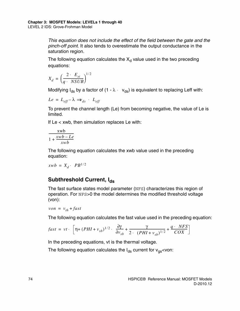
74 HSPICE® Reference Manual: MOSFET ModelsD-2010.12
Chapter 3: MOSFET Models: LEVELs 1 through 40LEVEL 2 IDS: Grove-Frohman Model
This equation does not include the effect of the field between the gate and the pinch-off point. It also tends to overestimate the output conductance in the saturation region.
The following equation calculates the Xd value used in the two preceding equations:
Modifying Ids by a factor of (1 - λ ⋅ vds) is equivalent to replacing Leff with:
To prevent the channel length (Le) from becoming negative, the value of Le is limited.
If Le < xwb, then simulation replaces Le with:
The following equation calculates the xwb value used in the preceding equation:
Subthreshold Current, Ids
The fast surface states model parameter (NFS) characterizes this region of operation. For NFS>0 the model determines the modified threshold voltage (von):
The following equation calculates the fast value used in the preceding equation:
In the preceding equations, vt is the thermal voltage.
The following equation calculates the Ids current for vgs<von:
Xd
2 Esi⋅q NSUB⋅--------------------------⎝ ⎠
⎛ ⎞1 2/
=
Le Leff λ ⇒vds Leff⋅–=
xwb
1xwb Le–
xwb----------------------+
--------------------------------
xwb Xd PB1 2/⋅=
von vth fast+=
fast vt η PHI vsb+( )1 2/ γ∂∂vsb----------⋅ γ
2 PHI vsb+( )1 2/⋅---------------------------------------------- q NFS⋅
COX---------------------+ + +⋅=

HSPICE® Reference Manual: MOSFET Models 75D-2010.12
Chapter 3: MOSFET Models: LEVELs 1 through 40LEVEL 3 IDS: Empirical Model
vgs>von:
The following equation calculates the vde value used in the preceding equation:
Note: The modified threshold voltage (von), due to NFS specification, is also used in strong inversion instead of vth, mostly in the mobility equations.
If WIC=3, the Level 2 model calculates the subthreshold current differently. In this case the Ids current is:
N0eff and NDeff are functions of effective device width and length.
LEVEL 3 IDS: Empirical Model
This section describes the LEVEL 3 IDS: Empirical model parameters and equations.
LEVEL 3 Model ParametersMOSFET Level 3 uses only the generic MOSFET model parameters described in Chapter 2, Common MOSFET Model Parameters.
LEVEL 3 Model EquationsThe LEVEL 3 model equations follow.
IDS EquationsThe following equations describe how the LEVEL 3 MOSFET model calculates the Ids drain current.
Cutoff Region, vgs < vth
Ids Ids von vde vsb, ,( ) evgs von–
fast----------------------
⋅=
Ids Ids vgs vde vsb, ,( )=
vde min vds vdsat,( )=
Ids Ids vgs vde vsb, ,( ) isub N0eff NDeff vgs vds, , ,( )+=

76 HSPICE® Reference Manual: MOSFET ModelsD-2010.12
Chapter 3: MOSFET Models: LEVELs 1 through 40LEVEL 3 IDS: Empirical Model
(See subthreshold current)
On Region, vgs >vth
The following equations calculate values used in the preceding equation:
Since
Note: In the above equation, the factor 4 should be 2, but because SPICE uses a factor of 4, this model uses a factor of 4 as well.
The fn parameter specifies the narrow width effect:
The fs term expresses the effect of the short channel:
Ids 0=
Ids β Vgs Vth1 fb+
2--------------– vde⋅–⎝ ⎠
⎛ ⎞ vde⋅ ⋅=
β K PWeffLeff------------ ueff COX
WeffLeff------------⋅ ⋅=⋅ ⋅=
K P⋅ ueff COX⋅=
vde min vds vdsat,( )=
fb fn
GAMMA fs⋅4 PHI vsb+( )1 2/⋅----------------------------------------------+=
fnDELTA
Weff------------------- 1
4---
2π Esi⋅COX
--------------------⋅ ⋅=
fs 1XJscaled
Leff------------------- ⇒
LDscaled Wc+
XJscaled---------------------------------- 1
Wp
XJscaled Wp+---------------------------------⎝ ⎠
⎛ ⎞2
–1 2/
⋅LDscaled
XJscaled---------------------–
⎩ ⎭⎪ ⎪⎨ ⎬⎪ ⎪⎧ ⎫
–=
Wp Xd PHI vsb+( )1 2/⋅=
Xd
2 Esi⋅q NSUB⋅--------------------------⎝ ⎠
⎛ ⎞1 2/
=
Wc XJscaled 0.0631353 0.8013292Wp
XJscaled-------------------⎝ ⎠
⎛ ⎞ 0.01110777⇒Wp
XJscaled-------------------⎝ ⎠
⎛ ⎞2
–⋅+⋅=

HSPICE® Reference Manual: MOSFET Models 77D-2010.12
Chapter 3: MOSFET Models: LEVELs 1 through 40LEVEL 3 IDS: Empirical Model
Effective Channel Length and WidthThe following equations determine the effective channel length and width in the LEVEL 3 model:
Threshold Voltage, vth
The following equation calculates the effective threshold voltage, including the device size and terminal voltage effects:
The following equation calculates the vbi value used in the preceding equation:
or
VTO is the extrapolated zero-bias threshold voltage of a large device. If you do not specify VTO, GAMMA, or PHI, simulation computes these values (see Common Threshold Voltage Equations on page 742).
Saturation Voltage, vdsat
The LEVEL 3 model determines the saturation voltage due to the channel pinch-off at the drain side.The VMAX parameter specifies the reduction of the saturation voltage due to the carrier velocity saturation effect.
The following equation calculates the vc value used in the preceding equations:
Leff Lscaled LMLT⋅ XLscaled 2 ⇒LDscaled DELscaled+( )–+=
Weff M Wscaled WMLT⋅ XWscaled 2 ⇒WDscaled–+( )⋅=
LREFF LREFscaled LMLT⋅ XLscaled 2 ⇒LDscaled DELscaled+( )–+=
WREFeff M WREFscaled WMLT⋅ XWscaled 2 ⇒WDscaled–+( )⋅=
vth vbi8.14e-22 ⇒ETA
COX Leff3⋅
--------------------------------------- ⇒vds– GAMMA fs PHI vsb+( )1 2/ fn PHI vsb+( )⋅+⋅ ⋅+=
vbi vfb PHI+= vbi VTO GAMMA ⇒PHI1 2/–=
vsat
vgs vth–
1 fb+-------------------=
vdsat vsat vc vsat2
vc2
+( )1 2/–+=

78 HSPICE® Reference Manual: MOSFET ModelsD-2010.12
Chapter 3: MOSFET Models: LEVELs 1 through 40LEVEL 3 IDS: Empirical Model
The next section defines the us surface mobility parameter. If you do not specify the VMAX model parameter, then:
Effective Mobility, ueff
The Level 3 model defines the carrier mobility reduction due to the normal field as the effective surface mobility (us).
vgs>vth
The VMAX model parameter model determines the degradation of mobility due to the lateral field and the carrier velocity saturation.
VMAX>0:
Otherwise,
Channel Length ModulationFor vds>vdsat, this model computes the channel length modulation factor. The VMAX model parameter value determines the amount of channel length reduction (ΔL).
VMAX=0
VMAX>0
vc
VMAX Leff⋅us
--------------------------------=
vdsat vsat=
usUO
1 THETA vgs vth–( )⋅+-------------------------------------------------------------=
ueffus
1vdevc
---------+------------------=
ueff us=
ΔL Xd KAPPA vds vdsat–( )⋅[ ]1 2/⋅=
ΔLEp Xd
2⋅2
-------------------–Ep Xd
2⋅2
-------------------⎝ ⎠⎜ ⎟⎛ ⎞
2
KAPPA Xd2
vds vdsat–( )⋅ ⋅+
1 2/
+=

HSPICE® Reference Manual: MOSFET Models 79D-2010.12
Chapter 3: MOSFET Models: LEVELs 1 through 40LEVEL 3 IDS: Empirical Model
In the preceding equation, Ep is the lateral electric field at the pinch off point. The following equation approximates its value:
The LEVEL 3 model modifies the Ids current to include the channel length modulation effect:
To prevent a zero denominator, the ΔL value is limited:
If then
Subthreshold Current, Ids
This region of operation is characterized by the model parameter for the fast surface state (NFS). The following equation determines the modified threshold voltage (von):
NFS>0
The following equation calculates the fast value used in the preceding equation:
The following equations calculate the Ids current:
vgs<von:
vgs>von:
Note: Strong inversion does not use the modified threshold voltage.
Ep
vc vc vdsat+( )⋅Leff vdsat⋅
---------------------------------------=
Ids
Ids
1ΔLLeff--------–
-----------------=
ΔLLeff
2--------> ΔL Leff
Leff
2--------⎝ ⎠
⎛ ⎞2
ΔL----------------–=
von vth fast+=
fast vtm 1q NFS⋅
COX---------------------
GAMMA fs PHI vsb+( )1 2/⋅ ⋅ fn PHI vsb+( )⋅+
2 PHI vsb+( )⋅----------------------------------------------------------------------------------------------------------------------------+ +⋅=
Ids Ids von vde vsb, ,( ) evgs von–
fast----------------------
⋅=
Ids Ids vgs vde vsb, ,( )=

80 HSPICE® Reference Manual: MOSFET ModelsD-2010.12
Chapter 3: MOSFET Models: LEVELs 1 through 40LEVEL 3 IDS: Empirical Model
If WIC=3, the model calculates subthreshold current differently. In this case, the Ids current is:
The isub subthreshold current for LEVEL=3 is the same as for LEVEL=13 (see ids Subthreshold Current on page 356).
N0eff and NDeff are functions of the effective device width and length.
Compatibility Notes
Synopsys Device Model versus SPICE3Differences between the Synopsys Level 3 MOSFET device model and Berkeley SPICE3 can arise in the following situations:
Small XJLEVEL 3 and SPICE3 differ for small XJ values, typically >0.05 microns. Do not use such small values for XJ; they are physically unreasonable. XJ calculates the short-channel reduction of the GAMMA effect:
fs is normally less than or equal to 1. For very small values of XJ, fs can be greater than one. The Synopsys Level 3 model imposes the limit fs £1.0, but SPICE3 allows fs>1.0.
ETAIn this model, 8.14 is the constant in the ETA equation, which varies the vds threshold. Berkeley SPICE3 uses 8.15.
Solution: To convert a SPICE3 model to the Synopsys Level 3 MOSFET device model, multiply ETA by 815/814.
NSUB MissingIf you do not specify NSUB in SPICE3, the KAPPA equation becomes inactive. The Synopsys Level 3 MOSFET model generates a default NSUB from GAMMA, and the KAPPA equation is active.
Solution: If you do not specify NSUB in the SPICE3 model, set KAPPA=0 in the Synopsys Level 3 MOSFET model.
Ids Ids vgs vde vsb, ,( ) isub N0eff NDeff vgs vds, , ,( )+=
GAMMA fs GAMMA⋅→

HSPICE® Reference Manual: MOSFET Models 81D-2010.12
Chapter 3: MOSFET Models: LEVELs 1 through 40LEVEL 3 IDS: Empirical Model
LD MissingIf you do not specify LD, simulation uses the default (0.75XJ). The SPICE3 default for LD is zero.
Solution: If you do not specify LD in the SPICE3 model, set LD=0 in the Level 3 MOSFET model.
Temperature CompensationThis example is based on demonstration netlist tempdep.sp, which is available in directory $<installdir>/demo/hspice/mos:
$ test of temp dependence for LEVEL=3 Tlevc=0 Tlev=1.option ingold=2 numdgt=6 post=2.temp 25 100vd d 0 5vg g 0 2m1 d g 0 0 nch w=10u L=1u.op.print id=lx4(m1) vdsat=lv10(m1).model nch nmos LEVEL=3 tlev=1 tlevc=0 acm=3+ uo=600 tox=172.6572+ vto=0.8 gamma=0.8 phi=0.64+ kappa=0 xj=0+ nsub=1e16 rsh=0+ tcv=1.5e-3 bex=-1.5.end
This simple model, with XJ=0 and KAPPA=0, has a saturation current:
Name Symbol Value
Boltzmann constant k =1.3806226e-23J⋅ K-1
Electron charge e =1.6021918e-19C
Permittivity of silicon dioxide
εox =3.45314379969e-11F/m
Permittivity of silicon εsi =1.035943139907e-10F/m

82 HSPICE® Reference Manual: MOSFET ModelsD-2010.12
Chapter 3: MOSFET Models: LEVELs 1 through 40LEVEL 3 IDS: Empirical Model
,
Using the model parameters in the input file, and the preceding equations, produces these results:
At room temperature:
At T=100:
,
Ids
beta 0.5 vgs vtm–( )2⋅ ⋅1 fb+
-------------------------------------------------------------=
beta COXWL-----⎝ ⎠
⎛ ⎞ UO t( )⋅ ⋅= fbGAMMA
4 phi t( )⋅( )----------------------------------=
beta 1.2e 3–( ) ttref---------⎝ ⎠
⎛ ⎞ BEX⋅=
vtm 0.8 TCV t tref–( )⋅–=
phi t( ) 0.64t
tref---------⎝ ⎠
⎛ ⎞ vtherm egarg 3t
tref---------⎝ ⎠
⎛ ⎞log⋅+⎝ ⎠⎛ ⎞⋅–⋅=
beta 1.2e 3–( )=
vtm 0.8=
phi t( ) 0.64=
Ids 1.2e 3–( ) 0.52 0.8–( )2
10.2
0.64--------------+
------------------------⋅ ⋅ 6.912e 4–= =
beta 1.2e 3–= 1.251551( ) 1.5–⋅ 0.570545e 4–=
vtm 0.8 1.5e 3–( ) 75⋅– 0.6875= =
egarg 9.399920= vtherm 3.215466e 2–=
phi t( ) 0.64 1.251551 0.3238962–⋅ 0.4770964= =
Ids beta 0.52 vt–( )2
10.2
phi t( )-------------------+
-----------------------------⋅ ⋅ 5.724507e 4–= =

HSPICE® Reference Manual: MOSFET Models 83D-2010.12
Chapter 3: MOSFET Models: LEVELs 1 through 40LEVEL 4 IDS: MOS Model
Simulation results:T=25, id=6.91200e-04
T=100, id=5.72451e-04
These results agree with the hand calculations.
LEVEL 4 IDS: MOS Model
The LEVEL 4 MOS model is the same as the LEVEL 2 model with the following exceptions:
■ No narrow width effects:
■ No short-channel effects:
■ For lateral diffusion, LDscaled=LD ⋅ XJ ⋅ SCALM. If you specify XJ, the LD default=0.75. If you do not specify XJ, the default is 0.
■ TPG, the model parameter for type of gate materials, defaults to zero (AL gate). The default is 1 for other levels. If you do not specify VTO, this parameter computes VTO (see Common Threshold Voltage Equations on page 742).
■ Starting in 2001.4.2, MOSFET LEVEL 4 and LEVEL 9 support both M and AREA scaling.
LEVEL 5 IDS Model
This section describes the LEVEL 5 IDS model parameters and equations.
Note: This model uses micrometer units rather than the typical meter units. Units and defaults are often unique in LEVEL 5. Level 5 does not use the SCALM option.
h=1
γ =GAMMA

84 HSPICE® Reference Manual: MOSFET ModelsD-2010.12
Chapter 3: MOSFET Models: LEVELs 1 through 40LEVEL 5 IDS Model
LEVEL 5 Model ParametersMOSFET Level 5 uses the generic MOSFET model parameters described in Chapter 2, Common MOSFET Model Parameters. It also uses the parameters described in this section, which apply only to MOSFET LEVEL 5.
Use the ZENH flag mode parameter to select one of two modes: enhancement or depletion.
The Synopsys enhancement and depletion modes are basically identical to the AMI models. However, the Synopsys enhancement and depletion modes let you choose either SPICE or ASPEC temperature compensation. ■ TLEV=1 (default) uses ASPEC-style temperature compensation. ■ TLEV=0 uses SPICE-style temperature compensation.
CAPOP=6 represents AMI Gate Capacitance in the Synopsys device models. CAPOP=6 is the default setting for LEVEL 5 only. LEVEL 5 models can also use CAPOP=1, 2, and 3.
Table 11 Capacitance Parameters for MOSFET Level 5
Name (Alias) Units Default Description
AFC 1.0 Area factor for MOSFET capacitance
CAPOP 6 Gate capacitance selector
METO μm 0.0 Metal overlap on gate
Parameter Description
ZENH=1 This enhancement model (default mode) is a portion of the Synopsys MOS5 device model, and is identical to AMI SPICE MOS LEVEL 4.
ZENH=0 This depletion model is revised in the Synopsys MOS5 device model (from previous depletion mode) and is identical to AMI SPICE MOS LEVEL 5.

HSPICE® Reference Manual: MOSFET Models 85D-2010.12
Chapter 3: MOSFET Models: LEVELs 1 through 40LEVEL 5 IDS Model
The ACM parameter defaults to 0 in LEVEL 5, invoking SPICE-style parasitics. You can also set ACM to 1 (ASPEC) or to 2 (Synopsys device models). All MOSFET models follow this convention.
You can use .OPTION SCALE with the LEVEL 5 model; however, you cannot use the SCALM option, due to the difference in units.
You must specify the following parameters for MOS LEVEL 5: VTO (VT), TOX, UO (UB), FRC, and NSUB (DNB).
IDS EquationsCutoff Region, vgs<vth
(See Subthreshold Current, Ids on page 88)
On Region, vgs>vth
The following equations calculate values used in the preceding equation:
The following equation calculates the gate oxide capacitances per unit area:
Effective Channel Length and WidthThe following equations determine the effective channel length and width in the LEVEL 5 model:
Ids 0=
Ids β vgs vbi–vde
2---------–⎝ ⎠
⎛ ⎞ vde23--- ⇒γ ⇒ Φf vde vsb+ +( )3 2/ Φf vsb+( )3 2/–[ ]
⎭⎬⎫
–⋅
⎩⎪⎨⎪⎧
⋅=
vde min vds vdsat,( )=
β UBeff coxWeff
Leff----------⋅ ⋅=
Φf 2 vtm lnDNB
ni------------⎝ ⎠
⎛ ⎞⋅ ⋅=
coxEox
TOX 1E-10⋅---------------------------------- F/m=
Weff Wscaled WMLT⋅ OXETCH+=

86 HSPICE® Reference Manual: MOSFET ModelsD-2010.12
Chapter 3: MOSFET Models: LEVELs 1 through 40LEVEL 5 IDS Model
Threshold Voltage, vth
The VTO model parameter is an extrapolated zero-bias threshold voltage for a large device. The following equation calculates the effective threshold voltage, including the device size effects and the terminal voltages:
The following equations calculate values used in the preceding equation:
Note: You must specify DNB and VTO parameters for the LEVEL 5 model. The Synopsys device model uses DNB to compute γ 0, and ignores the GAMMA model parameter.
The following equation computes the γ effective body effect, including the device size effects:
If SCM < 0, then scf=0.
Otherwise,
If NWM<0, then ncf=0.
Otherwise,
The following equation calculates the xd value used in the preceding equations:
Leff Lscaled LMLT 2 ⇒LATD DEL+( )–⋅=
vth vbi γ Φf vsb+( )1 2/⋅+=
vbi vfb Φf+ VTO γ 0 ⇒Φf1 2/–= =
γ 0
2 Esi q DNB⋅ ⋅ ⋅( )1 2/
cox-----------------------------------------------------------=
γ γ 0 1 scf–( ) 1 ncf+( )⋅ ⋅=
scfXJLeff-------- 1
2xdXJ--------- SCM vds⋅ vsb Φf+ +( )1 2/⋅+
1 2/1–
⎩ ⎭⎨ ⎬⎧ ⎫⋅=
ncfNWM Xd Φf( )1 2/⋅ ⋅
Weff----------------------------------------------------=
Xd
2 Esi⋅q DNB⋅-----------------------⎝ ⎠
⎛ ⎞1 2/
=

HSPICE® Reference Manual: MOSFET Models 87D-2010.12
Chapter 3: MOSFET Models: LEVELs 1 through 40LEVEL 5 IDS Model
Saturation Voltage, vdsat
The following equation computes the saturation voltage due to the channel pinch-off at the drain side:
If ECV does not equal 1000, the program modifies vsat to include the carrier velocity saturation effect:
, where
Mobility Reduction, UBeff
The following equation computes the mobility degradation effect in the LEVEL 5 MOSFET model:
The following equations calculate the Le value used in the preceding equation:
linear region
saturation region
The next section describes the ΔL channel length modulation effect.
Channel Length ModulationThe LEVEL 5 model modifies the Ids current to include the channel length modulation effect:
vsat vgs vbi–γ 2
2------ 1 1
4γ 2------ vgs vbi– Φf vsb+ +( )⋅+
1 2/–
⎩ ⎭⎨ ⎬⎧ ⎫⋅+=
vdsat vsat=
vdsat vsat vc vsat2
vc2
+( )1 2/–+=
vc ECV Leff⋅=
UBeff1
1UB--------
FRC vgs vth–( )⋅TOX
-------------------------------------------- vdeVST Le⋅----------------------- FSB vsb
1 2⁄⋅+ + +
-------------------------------------------------------------------------------------------------------------------------------=
Le Leff=
Le Leff ΔL–=

88 HSPICE® Reference Manual: MOSFET ModelsD-2010.12
Chapter 3: MOSFET Models: LEVELs 1 through 40LEVEL 5 IDS Model
The following equation calculates the ΔL value used in the preceding equation:
ΔL is in microns, if XJ is in microns and DNB is in cm-3.
Subthreshold Current, Ids
The Fast Surface State (FSS) characterizes this region of operation if it is greater than 1e10. The following equation then calculates the effective threshold voltage, separating the strong inversion region from the weak inversion region:
The following equation calculates the fast value used in the preceding equation:
In the preceding equations, vt is the thermal voltage.
The following equations calculate Ids.
Weak Inversion Region, vgs <vth
Strong Inversion Region, vgs>vth
Note: Strong inversion also use the modified threshold voltage (von) that FSS produces; that is, the mobility equations use von instead of vth.
Ids
Ids
1ΔLLeff--------–
-----------------=
ΔL 1e42.73e3 XJ⋅
DNB ln1e20DNB------------⎝ ⎠
⎛ ⎞⋅-------------------------------------------
1 3/
vds vdsat– PHI+( )1 3/ PHI1 3/–[ ]⋅ ⋅=
von vth fast+=
fast vtm 1q FSS⋅
cox-------------------- γ
2 Φf vsb+( )1 2/⋅----------------------------------------+ +⋅=
Ids von vde vsb, ,( ) evgs von–
fast----------------------
⋅=
Ids Ids vgs vde vsb, ,( )=

HSPICE® Reference Manual: MOSFET Models 89D-2010.12
Chapter 3: MOSFET Models: LEVELs 1 through 40LEVEL 5 IDS Model
Depletion Mode DC Model ZENH=0The LEVEL 5 MOS model uses depletion mode devices as the load element in contemporary standard n-channel technologies[2]. This model assumes a silicon gate construction with an ion implant used to obtain the depletion characteristics. A special model is required for depletion devices, because the implant used to create the negative threshold also results in a complicated impurity concentration profile in the substrate. The implant profile changes the basis for the traditional calculation of the QB bulk charge. The additional charge from the implant, QBI, must be calculated.
This implanted layer also forms an additional channel, offering a conductive pathway through the bulk silicon as well as through the surface channel. This second pathway can cause difficulties when trying to model a depletion device using existing MOS models.
The surface channel partially shields the bulk channel from the oxide interface, and the mobility of the bulk silicon can be substantially higher. Yet with all of these differences, a depletion model still can share the same theoretical basis as the Ihantola and Moll gradual channel model.
The depletion model differs from the Ihantola and Moll model:■ Implant charge accounted for.■ Finite implant thickness (DP).■ Assumes two channels: a surface channel and a bulk channel.■ Bulk channel has a bulk mobility (UH).■ Assumes that the bulk gain is different from the surface gain.
In the depletion model, the gain is lower at low gate voltages and higher at high gate voltages. Due to this variation in gain, the enhancement models cannot accurately represent a depletion device. The physical model for a depletion device is basically the same as an enhancement model, except that a one-step profile with DP depth approximates the depletion implant.
Due to the implant profile, simulation calculates the drain current equation by region. The MOSFET Level 5 model has three regions: depletion, enhancement, and partial enhancement.
Depletion Region, vgs - vfb < 0
The bulk channel dominates the low gate voltage region.
Enhancement Region, vgs - vfb > 0, vds < vgs - vfb

90 HSPICE® Reference Manual: MOSFET ModelsD-2010.12
Chapter 3: MOSFET Models: LEVELs 1 through 40LEVEL 5 IDS Model
High gate voltage and low drain voltage define the enhancement region. In this region, both channels are fully turned on.
Partial enhancement region, vgs - vfb > 0, vds > vgs - vfb
The region has high gate and drain voltages so the surface region is partially turned on and the bulk region is fully turned on.
IDS Equations, Depletion Model LEVEL 5Depletion, vgs-vfb <0
Enhancement, vgs-vfb >vde>0
Partial Enhancement, vgs-vfb<vde
The following equations calculate values used in the preceding equations:
Ids β1 q⎩⎨⎧
NI vde cav vgs vfb–( ) vdevde2
2-----------–⋅⋅+⋅ ⋅ ⋅=
23---– cav γ vde vsb Φd+ +( )3 2/ vsb Φd+( )3 2/–[ ]
⎭⎬⎫
⋅ ⋅ ⋅
Ids β1 q NI vde23--- Þcav Þγ Þ vde vsb Φd+ +( )3 2/ vsb Φd+( )3 2/–[ ]–⋅ ⋅
⎩ ⎭⎨ ⎬⎧ ⎫⋅=
β vgs vfb–( ) vdevde2
2-----------–⋅⋅
Ids β1 q NI vde cav vgs vfb–( ) vdevde2
2-----------–⋅⋅+⋅ ⋅
⎩⎨⎧
⋅=
23---– cav γ vde vsb Φd+ +( )3 2/ vsb Φd+( )3 2/–[ ]⋅ ⋅ ⋅
⎭⎬⎫
12---β β1 Þcav–⎝ ⎠
⎛ ⎞ vgs vfb–( )2⋅

HSPICE® Reference Manual: MOSFET Models 91D-2010.12
Chapter 3: MOSFET Models: LEVELs 1 through 40LEVEL 5 IDS Model
The following sections describe the saturation voltage, threshold voltage, and effective γ .
Threshold Voltage, vth
The VTO model parameter is an extrapolated zero-bias threshold voltage for a large device. The following equations calculate the effective threshold voltage, including the device size effects and the terminal voltages:
The following equations calculate values used in the preceding equation:
β1 UHWeff
Leff----------⋅=
β UBeff coxWeff
Leff----------⋅ ⋅=
cavcox cs⋅cox cs+---------------------=
cs2.77Esi
DP 1e-4⋅---------------------------=
Φd vtm lnDNB nd⋅
ni 2--------------------------⎝ ⎠
⎛ ⎞⋅=
ndNI 1e4⋅
DP-----------------------=
vde min vds vdsat,( )=
vth vfb βd ⇒vch γ ⇒Φd vsb+( )1 2/–[ ]–=
vfb VTO βd vch γ 0 ÞΦd1 2⁄
–( )⋅+=
βdUH cav⋅UB cox⋅-------------------------=
vchq NI⋅
cav----------------=
γ 0
2 Esi q na1⋅ ⋅ ⋅( )1 2/
cav--------------------------------------------------------=

92 HSPICE® Reference Manual: MOSFET ModelsD-2010.12
Chapter 3: MOSFET Models: LEVELs 1 through 40LEVEL 5 IDS Model
The following equation computes the effective γ , including the small device size effects:
The following equations calculate values used in the preceding equation:
If SCM ≤0, then scf=0. Otherwise,
If NWM ≤0, then ncf=0. Otherwise,
The following equation calculates the xd value used in the preceding equation:
Note: If vgs ≤ vth, the surface is inverted and a residual DC current exists. If vsb is large enough to make vth > vinth, then vth is the inversion threshold voltage. To determine the residual current, this model inserts vinth into the Ids, vsat, and mobility equation in place of vgs (except for vgs in the exponential term of the subthreshold current).
The inversion threshold voltage at a specified vsb is vinth, which the following equation computes:
na1nd DNB⋅nd DNB+--------------------------=
ndNI
DP 1e-4⋅---------------------------=
γ γ 0 1 scf–( ) 1 ncf+( )⋅ ⋅=
scfXJLeff-------- 1
2xdXJ--------- SCM vds vb Φd+ +⋅( )1 2/⋅+
1 2/1–
⎩ ⎭⎨ ⎬⎧ ⎫⋅=
ncfNWM Xd Φd
1 2/⋅ ⋅Weff
----------------------------------------------=
Xd
2 Esi⋅q DNB⋅-----------------------⎝ ⎠
⎛ ⎞1 2/
=
vinth vfbq NI⋅
cox----------------– vsb–=

HSPICE® Reference Manual: MOSFET Models 93D-2010.12
Chapter 3: MOSFET Models: LEVELs 1 through 40LEVEL 5 IDS Model
Saturation Voltage, vdsat
The following equation computes the saturation voltage (vsat):
IF ECV is not equal to 1000 (V/μm), the Synopsys device models modify vsat to include the carrier velocity saturation effect:
The following equation calculates the vc value used in the preceding equation:
Mobility Reduction, UBeff
The surface mobility (UB) depends on terminal voltages as follows:
The following equations calculate values used in the preceding equation:
Linear region
Saturation region
The next section describes the ΔL channel length modulation effect.
Channel Length Modulation Modify the Ids current to model the channel length modulation effect:
The following equation calculates the ΔL value used in the preceding equation:
vsat vgs vfb– vchγ 2
2------ 1 1
4γ 2------ vgs vfb– vch vsb Φd+ + +( )⋅+
1 2/–
⎩ ⎭⎨ ⎬⎧ ⎫⋅+ +=
vdsat vsat=
vdsat vsat vc vsat vc2
+( )1 2/–+=
vc ECV Leff⋅=
UBeff1
1UB--------
FRC vgs vth–( )⋅TOX
-------------------------------------------- vdeVST le⋅---------------------- FSB vsb
1 2⁄⋅+ + +
------------------------------------------------------------------------------------------------------------------------------=
Le Leff=
Le Leff ΔL–=
Ids
Ids
1ΔLLeff--------–
-----------------=

94 HSPICE® Reference Manual: MOSFET ModelsD-2010.12
Chapter 3: MOSFET Models: LEVELs 1 through 40LEVEL 5 IDS Model
The ΔL parameter is in microns, if XJ is in microns and na1 is in cm-3.
Subthreshold Current, Ids
If device leakage currents become important for operation near or below the normal threshold voltage, then this model considers the subthreshold characteristics. The Level 5 MOSFET model uses the subthreshold model only if the number of fast surface states (FSS) is greater than 1e10. The following equation determines the effective threshold voltage (von):
The following equation calculates the fast value used in the preceding equation:
If von < vinth, then simulation substitutes vinth for von.
Note: The Level 5 MOSFET device model uses the following subthreshold model only if vgs < von, and if the device is either in partial or full enhancement mode. Otherwise, it uses the model in enhancement mode (ZENH=1). The subthreshold current calculated below includes the residual DC current.
If vgs <von then:
Partial Enhancement, vgs-vfb < vde
ΔL 1e42.73e3 XJ⋅
na1 ln1e20na1------------⎝ ⎠
⎛ ⎞⋅----------------------------------------
1 3/
vds vdsat– PHI+( )1 3/ PHI1 3/–[ ]⋅ ⋅=
von vth fast+=
fast vtm 1q FSS⋅
cox-------------------- γ
2 Φd vsb+( )1 2/⋅-----------------------------------------+ +⋅=
Ids β1 q NI vde cav von vfb–( ) vdevde2
2-----------–⋅⋅+⋅ ⋅
⎩⎨⎧
⋅=
23---– cav γ vde vsb Φd+ +( )3 2/ vsb Φd+( )3 2/–[ ]
⎭⎬⎫
⋅ ⋅ ⋅

HSPICE® Reference Manual: MOSFET Models 95D-2010.12
Chapter 3: MOSFET Models: LEVELs 1 through 40LEVEL 5 IDS Model
Full Enhancement, vgs-vfb vde > 0
ExampleThis example is based on demonstration netlist m15iv.sp, which is available in directory $<installdir>/demo/hspice/mos:
FILE ML5IV.SP HSPICE LEVEL 5 MODEL EXAMPLES*OUTPUT CHARACTERISTICS FOR ENHANCEMENT & DEPLETION MODE.OPT ACCT LIST CO=132 POST=2.OPVDS 3 0 .1VGS 2 0M1 1 2 0 0 MODEN L=20U W=20U.MODEL MODEN NMOS LEVEL=5+ VT=.7 TOX=292 FRC=2.739E-2 DNB=2.423E16 UB=642.8+ OXETCH=-.98 XJ=.29 LATD=.34 ECV=4 VST=5.595E7+ FSB=7.095E-5 SCM=.4 FSS=2.2E11 NWM=.93 PHI=.61+ TCV=1.45E-3 PTC=9E-5 BEX=1.8*VIDS 3 1.DC VGS 0 5 0.2.PRINT DC I(VIDS) V(2).PRINT DC I(VIDS)$$$$$$.ALTER$$$$$$M1 1 2 0 0 MODDP L=20U W=20U.MODEL MODDP NMOS LEVEL=5 ZENH=0.+ VT=-4.0 FRC=.03 TOX=800 DNB=6E14 XJ=0.8 LATD=0.7+ DEL=0.4 CJ=0.1E-3 PHI=0.6 EXA=0.5 EXP=0.5 FSB=3E-5+ ECV=5 VST=4E7 UB=850 SCM=0.5 NI=5.5E11 DP=0.7 UH=1200*.END
12--- β e
vgs von–fast
----------------------⋅ β1 ⇒cav–
⎝ ⎠⎜ ⎟⎛ ⎞
von vfb–( )2⋅ ⋅
Ids β1 q NI vde23--- Þcav Þγ vde vsb Φd+ +( )3 2/ vsb Φd+( )3 2/–[ ]–⋅ ⋅
⎩ ⎭⎨ ⎬⎧ ⎫⋅=
β von vfb–( ) vdevde2
2-----------–⋅ e
vgs von–fast
----------------------⋅ ⋅

96 HSPICE® Reference Manual: MOSFET ModelsD-2010.12
Chapter 3: MOSFET Models: LEVELs 1 through 40LEVEL 6/LEVEL 7 IDS: MOSFET Model
LEVEL 6/LEVEL 7 IDS: MOSFET Model
These models represent ASPEC, MSINC, and ISPICE MOSFET model equations. The only difference between LEVEL 6 and LEVEL 7 equations is the handling of the parasitic elements and the method of temperature compensation. See Table 10 on page 61 and Channel Length Modulation on page 73 for those model parameters.
LEVEL 6 and LEVEL 7 Model ParametersMOSFET Levels 6 and 7 use the generic MOSFET model parameters described in Chapter 2, Common MOSFET Model Parameters. These levels also use the parameters described in this section, which apply only to MOSFET Levels 6 and 7.
UPDATE Parameter for LEVEL 6 and LEVEL 7The general form of the Ids equation for LEVEL 6 is the same as the LEVEL 2 MOS model. However, the small size effects, mobility reduction, and channel length modulation are included differently. Also, you can use the multi-level GAMMA capability to model MOS transistors with ion-implanted channels.
Table 12 Alternate Saturation Model Parameters
Name (Alias) Units Default Description
KA 1.0 Alternate saturation model: coefficient for the short-channel vds scaling factor.
KU 0.0 Lateral field mobility parameter.
MAL 0.5 Alternate saturation model: exponent of the short-channel vds scaling factor.
MBL 1.0 Exponent for mobility reduction due to the source-drain electric field.
NU 1.0 Mobility reduction due to the source-drain electric field.

HSPICE® Reference Manual: MOSFET Models 97D-2010.12
Chapter 3: MOSFET Models: LEVELs 1 through 40LEVEL 6/LEVEL 7 IDS: MOSFET Model
The LEVEL 6 model can represent the ASPEC, MSINC, or ISPICE MOSFET model. Use the UPDATE model parameter to invoke different versions of the LEVEL 6 model.
UPDATE=0This is the original Synopsys Level 6 MOSFET device model, which is not quite compatible with the ASPEC model. It has some discontinuities in the weak inversion, mobility equations (MOB=3), and multi-level GAMMA equations.
UPDATE=1This enhanced version of the LEVEL 6 model contains improved multi-level GAMMA equations. The saturation voltage, drain-source current, and conductances are continuous.
UPDATE=2This version of the LEVEL 6 model is compatible with the ASPEC model. The multi-level GAMMA model is not continuous as it is in the ASPEC program. See ASPEC Compatibility on page 123.■ Set UPDATE to 1.0 to use changes to the device equations. ■ Set UPDATE to 1.0 or 2 to use the default RS and RD handling.
These values and changes provide a more accurate ASPEC model.
UPDATE=1 or 2: TOX=690
UO (UB)=750 cm2/(V ⋅ s) (N-ch)
UTRA (F3)=0.0
UPDATE=0: TOX=1000
UO (UB)=750 cm2/(V ⋅ s) (N-ch)
UTRA (F3)=0.0
If you do not specify LDIF, then the RD and RS values change in the MOSFET:
UPDATE=1 or 2 and LDIF=0:
RDRD NRD RL⋅+( )
M----------------------------------------------=
RSRS NRS RL⋅+( )
M--------------------------------------------=

98 HSPICE® Reference Manual: MOSFET ModelsD-2010.12
Chapter 3: MOSFET Models: LEVELs 1 through 40LEVEL 6/LEVEL 7 IDS: MOSFET Model
Note: The ASPEC program does not use the M multiplier.
LDIF 0:
The vde value in the mobility equations change for the alternate saturation model:
, UPDATE=1 or 2
, UPDATE=0
The impact ionization equation calculates the saturation voltage:
, UPDATE=1 or 2
, UPDATE=0
The MOB=3 mobility equation changes:
UPDATE=1 or 2 and > VF1:
UPDATE=0 and > VF1:
LEVEL 6 Model Equations, UPDATE=0,2
IDS Equations
The following equations calculate values used in the preceding equation:
≠
RDLATDscaled LDIFscaled+
Weff----------------------------------------------------------------------- RD⋅ NRD
RLM-------⋅+=
RSLATDscaled LDIFscaled+
Weff----------------------------------------------------------------------- RS⋅ NRS
RLM-------⋅+=
vde minvdsvfa-------- vsat,⎝ ⎠
⎛ ⎞=
vde min vds vfa vsat⋅,( )=
vdsat vfa vsat⋅=
vdsat vsat=
vgs vth–( )F2
ueffUB
F4 F1 F3–( ) VF1 F3 vgs vth–( )F2⋅+⋅+--------------------------------------------------------------------------------------------------------------=
vgs vth–( )F2
ueffUB
F4 F3 vgs vth–( )F2⋅+------------------------------------------------------------=
ids β vgs vbi–η vde⋅
2------------------–⎝ ⎠
⎛ ⎞ vde23--- ⇒γ ⇒ PHI vde vsb+ +( )3 2/ PHI vsb+( )3 2/–[ ]–⋅
⎩ ⎭⎨ ⎬⎧ ⎫
⋅=

HSPICE® Reference Manual: MOSFET Models 99D-2010.12
Chapter 3: MOSFET Models: LEVELs 1 through 40LEVEL 6/LEVEL 7 IDS: MOSFET Model
■ The η, vbi, and γ values define the narrow-width effect. ■ The NWE or NWM model parameters also specify the narrow-width effect.■ The vbi and γ parameters specify the short-channel effect.
Effective Channel Length and WidthThe following equations calculate the effective channel length and width from the drawn length and width:
Threshold Voltage, vthThe following equation determines the effective threshold voltage:
The vbi and γ built-in voltage value depends on the specified model parameters.
Single-Gamma, VBO=0If you set the VBO model parameter to zero, simulation uses the single-gamma model, which treats the LGAMMA parameter as a junction depth. To modify the GAMMA parameter for the short-channel effect, this model then uses the scf factor, which the Poon and Yau formulation computes. In this case, simulation multiplies LGAMMA by the SCALM option.
vde min vds vdsat,( )=
η 1NWEscaled
weff------------------------------+=
β ueff COXweffLeff-----------⋅ ⋅=
leff Lscaled LMLT XLscaled 2 ⇒LDscaled DELscaled+( )–+⋅=
weff M Wscaled WMLT XWscaled 2 ⇒WDscaled–+⋅( )⋅=
LREFeff LREFscaled LMLT XLscaled 2 ⇒LDscaled DELscaled+( )–+⋅=
WREFeff M WREFscaled WMLT XWscaled 2 ⇒WDscaled–+⋅( )⋅=
vth vbi γ PHI vsb+( )1 2/⋅+=
scf 1LGAMMA
leff-------------------------- ⇒ 1
2 LAMBDA⋅LGAMMA
----------------------------------- PHI vsb+( )1 2/⋅+1 2/
1–⎩ ⎭⎨ ⎬⎧ ⎫–=

100 HSPICE® Reference Manual: MOSFET ModelsD-2010.12
Chapter 3: MOSFET Models: LEVELs 1 through 40LEVEL 6/LEVEL 7 IDS: MOSFET Model
The XJ model parameter modifies the GAMMA model parameter by the short-channel factor (gl):
The gl factor generally replaces the scf factor for the multi-level GAMMA model.
The gw factor modifies GAMMA to compute the narrow-width effect:
The following equation calculates the xd value used in the preceding equation:
Finally, the effective γ , including short-channel and narrow-width effects, is
Effective Built-in Voltage, vbiThe Level 6 model includes the narrow-width effect. This effect is the increase in threshold voltage due to the extra bulk charge at the edge of the channel. To use this effect with the NWE model parameter, modify vbi.
Modify vbi to use the short-channel effect, which decreases threshold voltage due to the induced potential barrier-lowering effect. To include this effect, you must specify either the FDS parameter, or the UFDS and VFDS model parameters.
The following equations calculate vbi, which sums up the preceding features.
vds<VFDS, or VFDS=0
vds>VFDS
gl 1XJscaled
leff------------------------ ⇒ 1
2 LAMBDA⋅XJscaled
----------------------------------- PHI vsb SCM vds⋅+ +( )1 2/⋅+1 2/
1–⎩ ⎭⎨ ⎬⎧ ⎫–=
gw1 NWM+ xd⋅
weff-------------------------------------=
xd2 ε si⋅
q DNB⋅-----------------------⎝ ⎠
⎛ ⎞ 1 2/=
γ GAMMA gw gl scf⋅ ⋅ ⋅=
vbi VTO γ ⇒PHI1 2/– η 1–( ) PHI vsb+( )⋅ LDscaledLeff
-------------------------
⇒VSHε si
COX Leff⋅------------------------------ ⇒FDS ⇒vds–
–+=
vbi VTO γ ⇒PHI1 2/– η 1–( ) PHI vsb+( )⋅ LDscaledleff
-------------------------⇒VSH–esi
COX Leff⋅--------------------------------–+=

HSPICE® Reference Manual: MOSFET Models 101D-2010.12
Chapter 3: MOSFET Models: LEVELs 1 through 40LEVEL 6/LEVEL 7 IDS: MOSFET Model
The preceding equations describe piecewise linear variations of vbi as a function of vds. If you do not specify VFDS, this model uses the first equation for vbi.
Note: The Level 6 MOSFET device model calculates model parameters such as VTO, PHI, and GAMMA, if you did not specify them (see Common Threshold Voltage Parameters on page 742).
Multi-Level Gamma, VBO>0Use Multi-Level Gamma to model MOS transistors with Ion-Implanted channels. The doping concentration under the gate is approximated as step functions. ■ GAMMA represents the corresponding body effects coefficient for the implant
layer.■ LGAMMA represents the corresponding body effects coefficient for the
substrate.
Figure 2 shows the variation of vth as a function of vsb for Multi-Level Gamma.
Figure 2 Threshold Voltage Variation
The following equations calculate the threshold voltage for different regions:
Channel Depletion Region is in the Implant Layer, vsb<VBO
FDS UFDS–( ) VFDS UFDS vds⋅+⋅[ ]
Vsb=VBO
Slope = γ b
Slope = γ i
Vth
Vtb
VTO
(PHI+Vsb)1/2-PHI1/2

102 HSPICE® Reference Manual: MOSFET ModelsD-2010.12
Chapter 3: MOSFET Models: LEVELs 1 through 40LEVEL 6/LEVEL 7 IDS: MOSFET Model
Channel Depletion Region Expands into the Bulk, vsb>VBO
For the threshold voltage to be continuous at vsb=VBO, vtb must be:
■ γ i is the effective value of GAMMA.■ γ b is the effective value of LGAMMA.
The model computes them as γ in single-gamma models, except the scf factor is 1.0.
Effective Built-in Voltage, vbi for VBO>0For vds<VFDSif vsb≤VBO:
if vsb>VBO:
For vds>VFDSif vsb≤VBO:
γ γ i=
vth vbi γ i vsb PHI+( )1 2/⋅+=
vbi VTO γ i ⇒PHI( )1 2/–=
γ γ b=
vth vbi γ b vsb PHI+( )1 2/⋅+=
vbi vtb γ b ⇒PHI( )1 2/–=
vtb VTO γ i γ b–( ) VBO PHI+( )1 2/ PHI( )1 2/–[ ]⋅+=
γ i GAMMA gw gl⋅ ⋅=
γ b LGAMMA gw gl⋅ ⋅=
vbi VTO γ i ⇒PHI( )1 2/– η 1–( ) PHI vsb+( )⋅ LDscaledLeff
-------------------------
⇒VSHε si
COX Leff⋅------------------------------ ⇒FDS ⇒vds–
–+=
vbi VTO γ b ⇒PHI( )1 2/– γ i γ b–( ) VBO PHI+( )1 2/ PHI( )1 2/–[ ] η 1–( )+⋅+=
PHI vsb+( ) LDscaledLeff
------------------------- ⇒VSH–ε si
COX Leff⋅------------------------------ ⇒FDS ⇒vds–

HSPICE® Reference Manual: MOSFET Models 103D-2010.12
Chapter 3: MOSFET Models: LEVELs 1 through 40LEVEL 6/LEVEL 7 IDS: MOSFET Model
if vsb>VBO:
Saturation Voltage, vdsat (UPDATE=0,2)The following formula determines the saturation voltage due to channel pinch-off at the drain side:
The following equation calculates the reduction of the saturation voltage due to the carrier velocity saturation effect:
In the preceding equation, determines vc if the ECRIT model parameter >0, or VMAX >0, and KU≤1. If you specify both ECRIT and VMAX, then simulation uses only the VMAX equation. However, this model does not use the VMAX equation if MOB=4 or MOB=5, because these mobility equations already contain a velocity saturation term.
or
Because vsb>VBO, γ switches from γ ι to γ β, and the ids, vsat, and conductance values are not continuous as in the following example. To correct this discontinuity problem, specify the UPDATE=1 model parameter. The next section discusses this improvement.
vbi VTO γ i ⇒PHI( )1 2/– η 1–( ) PHI vsb+( )⋅
LDscaledLeff
------------------------- ⇒VSH–ε si
COX Leff⋅------------------------------–
+=
FDS UFDS–( ) VFDS UFDS vds⋅+⋅[ ]
vbi VTO γ b ⇒PHI( )1 2/– γ i γ b–( ) VBO PHI+( )1 2/
PHI( )1 2/–[
] η 1–( )+⋅+=
PHI vsb+LDscaled
Leff------------------------- ⇒VSH
ε siCOX Leff⋅------------------------------
⇒ FDS UFDS–( ) VFDS UFDS vds⋅+⋅[ ]
––
vsatvgs vbi–
η---------------------- 1
2--- γ
η---⎝ ⎠
⎛ ⎞ 21 1
2 η⋅γ
------------⎝ ⎠⎛ ⎞ 2 vgs vbi–
η---------------------- PHI vsb+ +⎝ ⎠
⎛ ⎞⋅+1 2/
–⎩ ⎭⎨ ⎬⎧ ⎫⋅+=
vdsat vsat vc vsat2 vc2+( )1 2/–+=
vc ECRIT Leff⋅= vcVMAX Leff⋅
ueff----------------------------------=

104 HSPICE® Reference Manual: MOSFET ModelsD-2010.12
Chapter 3: MOSFET Models: LEVELs 1 through 40LEVEL 6/LEVEL 7 IDS: MOSFET Model
ExampleThis example is based on demonstration netlist tgam2.sp, which is available in directory $<installdir>/demo/hspice/mos:
$ tgam2.sp---multi-level gamma model* this data is for the comparison of multi-level gamma* update=0 or 2 and the improved multi-level gamma update=1.*.options post aspec nomod vntol=.1u reli=.001 relv=.0001*.model nch nmos bulk=99 update=2+ fds=0.9 ku=1.6 mal=0.5 mob=1 clm=1+ latd=0.2 phi=0.3 vt=0.9 gamma=0.72 lgamma=0.14+ vb0=1.2 f1=0.08 esat=8.6e+4 kl=0.05+lambda=3.2u ub=638 f3=0.22+ ka=0.97 mbl=0.76 nfs=1.0e+12 wic=0+ ldel=0.084 wdel=0.037 tox=365 vsh=0.7*vd 1 0 5vb 0 99 0vg 2 0 1ma 1 2 0 99 nch 26.0 1.4.dc vb 1.0 1.3 .01.probe ids=par('i(ma)') vth=par('lv9(ma)') vdsat=par('lv10(ma)').probe gm=par('lx7(ma)') ds=par('lx8(ma)') gmbs=par('lx9(ma)').end

HSPICE® Reference Manual: MOSFET Models 105D-2010.12
Chapter 3: MOSFET Models: LEVELs 1 through 40LEVEL 6/LEVEL 7 IDS: MOSFET Model
Figure 3 Variation of IDS, VTH and VDSAT for UPDATE=0
1.0

106 HSPICE® Reference Manual: MOSFET ModelsD-2010.12
Chapter 3: MOSFET Models: LEVELs 1 through 40LEVEL 6/LEVEL 7 IDS: MOSFET Model
Figure 4 Variation of GM, GDS and GMBS for UPDATE=0
Each plot compares IDS, VTH, VDSAT, GM, GDS and GMBS as a function of vsb for UPDATE=0.
Improved Multi-Level Gamma, UPDATE=1As demonstrated in previous sections, the regular Multi-Level Gamma displays some discontinuities in saturation voltage and drain current. This occurs because when vsb is less than VBO, simulation sets γ to γ i and uses it to calculate ids and vsat. This is not correct; if (vds + vsb) exceeds VBO, then the depletion regions at the drain side expands into the substrate region, and the vsat computation must use γ b instead of γ i. Because vsat=vgs - vth (drain), this model uses γ i to compute the threshold voltage at the drain for vsb<VBO. As a result, the existing model overestimates the threshold voltage ( ), and underestimates the saturation voltage and the drain current in the saturation region.
This causes a discontinuous increase in the saturation drain current, crossing from the vsb<VBO region to the vsb>VBO region.
γ i γ b>

HSPICE® Reference Manual: MOSFET Models 107D-2010.12
Chapter 3: MOSFET Models: LEVELs 1 through 40LEVEL 6/LEVEL 7 IDS: MOSFET Model
The improved Multi-Level model upgrades the saturation voltage and drain current equations, compared to the regular Multi-Level model. To use the improved model, set the model parameter to UPDATE=1.
ExampleYou can see an example of a multi-level gamma model with UPDATE=2 using a netlist from a previous example. Change UPDATE=0 to UPDATE=2 in the netlist located in directory $installdir/demo/hspice/mos/tgam2.sp:
$ tgam2.sp---multi-level gamma model* this data is for the comparison of multi-level gamma* update=0 or 2 and the improved multi-level gamma update=1.*.options post aspec nomod vntol=.1u reli=.001 relv=.0001*.model nch nmos bulk=99 update=2+ fds=0.9 ku=1.6 mal=0.5 mob=1 clm=1+ latd=0.2 phi=0.3 vt=0.9 gamma=0.72 lgamma=0.14+ vb0=1.2 f1=0.08 esat=8.6e+4 kl=0.05+lambda=3.2u ub=638 f3=0.22+ ka=0.97 mbl=0.76 nfs=1.0e+12 wic=0+ ldel=0.084 wdel=0.037 tox=365 vsh=0.7*vd 1 0 5vb 0 99 0vg 2 0 1ma 1 2 0 99 nch 26.0 1.4.dc vb 1.0 1.3 .01.probe ids=par('i(ma)') vth=par('lv9(ma)') vdsat=par('lv10(ma)').probe gm=par('lx7(ma)') ds=par('lx8(ma)') gmbs=par('lx9(ma)').end

108 HSPICE® Reference Manual: MOSFET ModelsD-2010.12
Chapter 3: MOSFET Models: LEVELs 1 through 40LEVEL 6/LEVEL 7 IDS: MOSFET Model
Figure 5 Variation of IDS, VTH and VDSAT for UPDATE=2
720.0M
55.0U
1.01.050 1.10 1.2501.20
1.30VOLTS (LIN)
TGAM2.SP MULT-LEVEL GAMMA MODEL, UPDATE=214 MAY 2003 15:46:38 TGAM2.SW0
IDS
1.150
47.6009U
PA
AM
RLIN
PA
AM
RLIN
PA
AM
RLIN
TGAM2.SW0VTH
TGAM2.SW0VDSAT
52.50U
50.0U
235.146M
700.0M
680.0M
245.0M
240.0M

HSPICE® Reference Manual: MOSFET Models 109D-2010.12
Chapter 3: MOSFET Models: LEVELs 1 through 40LEVEL 6/LEVEL 7 IDS: MOSFET Model
Figure 6 Variation of GM, GDS and GMBS for UPDATE=2
Each plot compares IDS, VTH, VDSAT, GM, GDS, and GMBS as a function of vsb for UPDATE=1.
Saturation Voltage, vsatTo obtain the right value for vsat, the following equations calculate two trial values of vsat corresponding to γ i and γ b:
■ vbi1 is the built-in potential corresponding to γ i.■ vbi2 is the built-in potential corresponding to γ b.
vsat1vgs vbi1–
η-------------------------- 1
2--- γ i
η-----⎝ ⎠
⎛ ⎞ 21 1
2 η⋅γ i
------------⎝ ⎠⎛ ⎞ 2 vgs vbi1–
η-------------------------- PHI vsb+ +⎝ ⎠
⎛ ⎞⋅+1 2/
–⎩ ⎭⎨ ⎬⎧ ⎫⋅+=
vsat2vgs vbi2–
η-------------------------- 1
2--- γ b
η------⎝ ⎠
⎛ ⎞ 21 1
2 η⋅γ b
------------⎝ ⎠⎛ ⎞ 2 vgs vbi2–
η-------------------------- PHI vsb+ +⎝ ⎠
⎛ ⎞⋅+1 2/
–⎩ ⎭⎨ ⎬⎧ ⎫⋅+=

110 HSPICE® Reference Manual: MOSFET ModelsD-2010.12
Chapter 3: MOSFET Models: LEVELs 1 through 40LEVEL 6/LEVEL 7 IDS: MOSFET Model
■ If (vdsat1 + vsb) ≤ VBO, then vdsat=vdsat1■ If (vdsat2 + vsb) > VBO, then vdsat=vdsat2
To obtain vdsat, vc modifies vsat for the carrier velocity saturation.
LEVEL 6 IDS Equations, UPDATE=1You can use one of three equations for ids, depending on the region of operation. To derive these equations, this model integrates the bulk charge (vgs - vth (v) - v) from the source to the drain.
For vsb<VBO-vde, the model forms an entire gate depletion region in the implant layer.
In the preceding equation, vbi1 is the same as vbi for vsb≤VBO.
For vsb ≥ VBO, the entire gate depletion region expands into the bulk area.
In the preceding equation, vbi2 is the same as vbi for vsb>VBO.
For VBO-vde<vsb<VBO, the source side gate depletion region is in the implant layer, but the drain side gate depletion region expands into the bulk area.
ids β vgs vbi1–η vde⋅
2------------------–⎝ ⎠
⎛ ⎞ vde23---– γ i PHI vde vsb+ +( )3 2/ PHI vsb+( )3 2/–[ ]
⎭⎬⎫⋅ ⋅⋅
⎩⎪⎨⎪⎧
⋅=
ids β vgs vbi2–η vde⋅
2------------------–⎝ ⎠
⎛ ⎞ vde 23---– γ b PHI vde vsb+ +( )3 2/ PHI vsb+( )3 2/–[ ]
⎭⎬⎫
⋅ ⋅⋅
⎩⎪⎨⎪⎧
⋅=
ids β vgs vbi2–η vde⋅
2------------------–( ) vde
23--- yi VBO PHI+( )3 2/ vsb PHI+( )3 2/–[ ]⋅ ⋅–⋅
⎩ ⎭⎨ ⎬⎧ ⎫
⋅=
γ i γ b–( ) VBO PHI+( )1 2/ VBO vsb–⎝ ⎠⎛ ⎞
⎭⎬⎫
⋅ ⋅+

HSPICE® Reference Manual: MOSFET Models 111D-2010.12
Chapter 3: MOSFET Models: LEVELs 1 through 40LEVEL 6/LEVEL 7 IDS: MOSFET Model
Alternate DC Model (ISPICE model)To invoke this model, set the KU>1 model parameter. Then, the model computes vfu and vfa scale factors to scale both the vds voltage and the ids current. These scale factors are functions of ECRIT and the vgs voltage. The following equations compute the vfa and vfu factors:
The following equation calculates the α value used in the preceding equations:
Note: The vfu factor is always less than one.
The following equation modifies the ids current:
NU=1
For NU=0, the
factor is set to one.
The ids current is a function of the effective drain to source voltage (vde):
This alternate model is generally coupled with the mobility normal field equations (MOB=3) and the channel length modulation drain field equation (CLM=3).
The mobility equations use the following vde and vds values:
, UPDATE=0
, UPDATE=1,2
vfu 1KU
α2 KU2+( )1 2/ α KU 1–( )+-------------------------------------------------------------------–=
vfa KA vfu 2 MAL⋅( )⋅=
α ECRIT Leff⋅vgs vth–
-----------------------------------=
ids vfu 2 MBL⋅( ) ids⋅=
vfu 2 MBL⋅( )
vde min vds/vfa vsat,( )=
vdsat vfa vsat⋅=
vde min vds vfa vsat⋅,( )=
vds min vds/vfa vsat,( )=

112 HSPICE® Reference Manual: MOSFET ModelsD-2010.12
Chapter 3: MOSFET Models: LEVELs 1 through 40LEVEL 6/LEVEL 7 IDS: MOSFET Model
Subthreshold Current, idsis the choice of two different equations, selected through The WIC (Weak Inversion Choice) model parameter characterizes this region of operation.
In addition to WIC, set the NFS parameter. NFS represents the number of fast states per centimeter squared. Reasonable values for NFS range from 1e10 to 1e12.
WIC=0No weak inversion.
WIC=1The vth threshold voltage increases by the fast term.
The following equation calculates the fast value used in the preceding equation:
In the preceding equations, vt is the thermal voltage. The following equation specifies the ids current for vgs<von:
if vgs<von, then
Note: Strong inversion conditions do not use the modified threshold voltage (von).
Parameter Description
WIC=0 No weak inversion (default)
WIC=1 ASPEC-style weak inversion
WIC=2 Enhanced HSPICE-style weak inversion
von vth fast+=
fast vt 1q NFS⋅
COX--------------------- γ
2 vsb PHI+( )1 2/⋅------------------------------------------------+ +⋅=
ids ids von vde vsb, ,( ) evgs von–
fast------------------------
⋅=
ids ids vge vde vsb, ,( )=

HSPICE® Reference Manual: MOSFET Models 113D-2010.12
Chapter 3: MOSFET Models: LEVELs 1 through 40LEVEL 6/LEVEL 7 IDS: MOSFET Model
WIC=2The subthreshold region is limited between the cutoff region and the strong inversion region. If the gate voltage is less than vth-PHI, this model cannot include any weak inversion conduction. However, this model can still include diffusion conduction from the drain-to-bulk rather than from the drain-to-source.
The following equation calculates the fast value used in the preceding equation:
Cutoff Region, vgs ≤ vth - PHI
Weak Inversion, vth - PHI < vgs ≤ von
Strong Inversion, vgs > von
Note: Strong inversion conditions do not use the modified threshold voltage (von).
WIC=3If WIC=3, simulation calculates the subthreshold current differently. In this case, the ids current is:
N0eff and NDeff are functions of the effective device width and length.
Effective Mobility, ueffAll mobility equations have the following general form:
Parameter Description
UEFF Effective mobility at the specified a specified analysis temperature.
von vth fast+=
fast vt 1q NFS⋅
COX--------------------- γ
2 vsb PHI+( )1 2/⋅------------------------------------------------+ +⋅=
ids 0=
ids ids von vde vsb, ,( ) 1von vgs–fast PHI+--------------------------–⎝ ⎠
⎛ ⎞ WEX⋅=
ids ids vgs vde vsb, ,( )=
ids ids vgs vde vsb, ,( ) isub N0eff NDeff vgs vds, , ,( )+=
ueff UO factor⋅=

114 HSPICE® Reference Manual: MOSFET ModelsD-2010.12
Chapter 3: MOSFET Models: LEVELs 1 through 40LEVEL 6/LEVEL 7 IDS: MOSFET Model
Use the MOB model parameter to select the mobility modulation equation used in the Level 6 MOSFET model.
The following sections describe these equations.
MOB=0 Default, No MobilityFACTOR=1.0 No mobility reduction
MOB=1
Use the MOB=1 equation for transistors with constant source-to-bulk voltage, because the factor does not contain a vsb term. This equation sometimes over-
FACTOR Mobility degradation factor. Default=1.0
Parameter Description
MOB=0 No mobility reduction (default)
MOB=1 Gm equation
MOB=2 Frohman-Bentchkowski equation
MOB=3 Normal field equation
MOB=4 Universal field mobility reduction
MOB=5 Universal field mobility reduction with an independent drain field
MOB=6 Modified MOB=3 equations (lateral field effect included)
MOB=7 Modified MOB=3 equations (lateral field effect not included)
Table 13 MOB=1 Gm Equation
Name (Alias) Units Default Description
F1 1/V 0.0 Gate field mobility reduction
UTRA (F3) factor 0.0 Source-drain mobility reduction factor
Parameter Description

HSPICE® Reference Manual: MOSFET Models 115D-2010.12
Chapter 3: MOSFET Models: LEVELs 1 through 40LEVEL 6/LEVEL 7 IDS: MOSFET Model
estimates mobility for small gate voltages and large back-bias, such as depletion pull-ups.
Note: In the alternate saturation model, vde is different if UPDATE=0 than if UPDATE=1. See Alternate DC Model (ISPICE model) on page 111. Also, if VMAX>0, then vde=min (vds, vsat). If you do not specify VMAX, then vde=min (vds, vdsat).
MOB=2
The mobility reduction equation (MOB=2)[3] produces good results for high gate voltages and drain fields with constant back-bias. Typically, you can use this equation for p-channel pull-ups and n-channel pull-downs. The VMAX value selects the proper vdsat calculation scheme. MOB=2 (SPICE default) corresponds to MSINC UN=2.
vde is the same in this equation as in the MOB=1 equation.
Table 14 MOB=2 Frohman-Bentchkowski Equation
Name (Alias) Units Default Description
F1 V/cm 0.0 Critical gate-bulk electric field at which mobility reduction becomes significant.
UEXP (F2) 0.0 Mobility exponent. Use a factor of 0.36 for n-channel and 0.15 for p-channel.
UTRA (F3) factor 0.0 Source-drain mobility reduction factor.
VMAX (VMX) cm/s 0.0 Maximum drift velocity of carriers. The VMAX setting determines which calculation scheme vdsat uses. Zero indicates an infinite value.
factor1
1 F1 vgs vb1– F3 ⇒vde–( )⋅+---------------------------------------------------------------------------------=
vde min vds vdsat,( )=
factorF1 ε si⋅
COX vgs vbi– F3 ⇒vde–( )⋅----------------------------------------------------------------------------
F2=

116 HSPICE® Reference Manual: MOSFET ModelsD-2010.12
Chapter 3: MOSFET Models: LEVELs 1 through 40LEVEL 6/LEVEL 7 IDS: MOSFET Model
MOB=3
This equation is the same as MSINC UN=1:
≤ VF1:
If UPDATE=0, and (vgs-vth)F2 > VF1:
If UPDATE=1, 2 and (vgs-vth)F2 > VF1:
Table 15 MOB=3 Normal Field Equation
Name (Alias) Units Default Description
F1 1/V 0.0 Low-field mobility multiplier
F4 1.0 Mobility summing constant
UEXP (F2) 0.0 Mobility exponent
UTRA (F3) 1/V 0.0 High-field mobility multiplier
VF1 V 0.0 Low to high field mobility (voltage switch)
vgs vth–( )F2
factor1
F4 F1 vgs vth–( )F2⋅+------------------------------------------------------------=
factor1
F4 F3 vgs vth–( )F2⋅+------------------------------------------------------------=
factor1
F4 F1 F3–( ) VF1⋅ F3 vgs vth–( )F2⋅+ +--------------------------------------------------------------------------------------------------------------=

HSPICE® Reference Manual: MOSFET Models 117D-2010.12
Chapter 3: MOSFET Models: LEVELs 1 through 40LEVEL 6/LEVEL 7 IDS: MOSFET Model
MOB=4
The MOB=4 equation is the same as the MSINC UN=3 equation.
MOB=5The MOB=5 equation is the same as MOB=4, except that F3 substitutes for ECRIT in the vc expression.
The MOB=5 equation provides a better fit for CMOS devices in the saturation region. Do not specify a VMAX value, because the mobility equation calculates the velocity saturation.
■ If MOB=4, then
■ If MOB=5, then
Table 16 MOB=4 and MOB=5 Universal Field Mobility Reduction
Name (Alias)Units Default Description
ECRIT V/cm 0.0 Critical electric drain field for mobility reduction. Zero indicates an infinite value.
F1 V/cm 0.0 Source-drain mobility reduction field (typical values are 1e4 to 5e8).
MOB 0.0 Selects a mobility equation:■ Set MOB=4 for the critical field equation. ■ Set MOB=5 for the critical field equation with
an independent drain field.
UEXP (F2) 1/V1/2 0.0 Bulk mobility reduction factor (typical values are 0 to 0.5).
UTRA (F3) V/cm 0.0 Critical electric drain field for mobility reduction.
factor1
1COX
F1 ε ox⋅----------------------- vgs cth–( )⋅ vde
vc--------- F2 vsb PHI+( )1 2/⋅+ + +
----------------------------------------------------------------------------------------------------------------------------------------------=
vc ECRIT Leff⋅=
vc F3 Leff⋅=

118 HSPICE® Reference Manual: MOSFET ModelsD-2010.12
Chapter 3: MOSFET Models: LEVELs 1 through 40LEVEL 6/LEVEL 7 IDS: MOSFET Model
Note: If you use the alternate saturation model, vde is different for UPDATE=0 than it is for UPDATE=1, 2.
MOB=6, 7 Modified MOB=3:This mobility equation is the same as MOB=3, except that the equation uses VTO instead of vth. If you specify MOB=6, the following equation modifies the ids current:
Channel Length ModulationThe basic MOSFET current equation for ids describes a parabola, where the peak corresponds to the drain-to-source saturation voltage (vdsat). Long-channel MOSFETs generally demonstrate ideal behavior. For vds voltages greater than vdsat, ids current does not increase. As channel length decreases, current in the saturation region continues to increase.
The simulator models this increase in current as a decrease in the effective channel length. Except for CLM=5 and 6, this model calculates the channel length modulation equations only when the device is in the saturation region.
The Level 6 MOSFET model provides several channel length modulation equations; all (except CLM=5) modify the ids equation:
ΔL is the change in channel length due to MOSFET electric fields.
The CLM model parameter designates the channel length modulation equation for the Level 6 MOSFET device model:
Parameter Description
CLM=0 No channel length modulation (default)
CLM=1 One-sided step depletion layer drain field equation
CLM=2 Frohman’s electrostatic fringing field equation
idsids
1 F1 vgs vth–vde2
---------–⎝ ⎠⎛ ⎞⋅ UTRA
Leff---------------- vde⋅+ +
----------------------------------------------------------------------------------------------------------=
idsids
1ΔL
Leff----------–
-------------------=

HSPICE® Reference Manual: MOSFET Models 119D-2010.12
Chapter 3: MOSFET Models: LEVELs 1 through 40LEVEL 6/LEVEL 7 IDS: MOSFET Model
The following sections describe these equations and the associated model parameters.
CLM=0 No Channel Modulation—Default
This is the default channel length equation, representing no channel length modulation; it corresponds to MSINC GDS=0.0.
CLM=1
If you do not specify LAMBDA, simulation calculates it as:
CLM=3 One-sided step depletion layer drain field equation with carrier velocity saturation
CLM=4 Wang’s equation: linearly graded depletion layer
CLM=5 Synopsys channel length modulation
CLM=6 Synopsys L equations
Table 17 CLM=1 Step Depletion Equation for MOSFET Level 6
Name (Alias) Units Default Description
KL 0.0 Empirical constant (saturation voltage)
LAMBDA (LAM, LA) cm/V1/2 1.137e-4 Channel length modulation. If you do not specify s, simulation calculates it from NSUB. The default LAMBDA corresponds to the default NSUB value.
Parameter Description
Δ
ΔL 0=
ΔL LAMBDA vds vdsat–( )1 2/ vdsatvsat
--------------⎝ ⎠⎛ ⎞ KL
⋅ ⋅=
LAMBDA2 ε si⋅
q DNB⋅-----------------------⎝ ⎠
⎛ ⎞ 1 2/=

120 HSPICE® Reference Manual: MOSFET ModelsD-2010.12
Chapter 3: MOSFET Models: LEVELs 1 through 40LEVEL 6/LEVEL 7 IDS: MOSFET Model
This is a one-sided step depletion region formulation by Grove: ΔL varies with the depletion layer width, which is a function of the difference between the effective saturation voltage (vdsat) and the drain-to-source channel voltage (vds). Typically, you can use this equation for long channels and high dopant concentrations. This corresponds to GDS=1 in MSINC.
CLM=2
You can use the fringing field equation or electrostatic channel length reduction (developed by Frohman-Bentchkowski) to model short-channel enhancement transistors. In MSINC, the equivalent equation is GDS=2.
Table 18 CLM=2 Electrostatic Fringing Field
Name (Alias) Units Default Description
A1 0.2 First fringing field factor, gate-drain
A2 0.6 Second fringing field factor, gate-vdsat
ΔLε si
COX------------ vds vdsat–
A1 vds vgs– vbi+( )⋅ A2 vgs vbi– vdsat–( )⋅+-----------------------------------------------------------------------------------------------------------------------------⋅=

HSPICE® Reference Manual: MOSFET Models 121D-2010.12
Chapter 3: MOSFET Models: LEVELs 1 through 40LEVEL 6/LEVEL 7 IDS: MOSFET Model
CLM=3
This equation is an extension of the first depletion layer equation, CLM=1. It includes effects of carrier velocity saturation, and source-to-bulk voltage (vsb) depletion layer width. It represents the basic ISPICE equation. See Alternate DC Model (ISPICE model) on page 111 for definitions of vfa and vfu.
Table 19 CLM=3 Carrier Velocity Saturation for MOSFET Level 6
Name (Alias) Units Default Description
KA 1.0 vds scaling factor for velocity saturation.
KCL 1.0 Exponent for vsb scaling factor.
KU 0.0 Velocity saturation switch. If KU ≤ 1, simulation uses the standard velocity saturation equation.
LAMBDA (LAM, LA) cm/V1/2 1.137e-4 Channel length modulation. If you do not specify LAMBDA, simulation calculates it from NSUB. The default LAMBDA corresponds to the default NSUB value.
MAL 0.5 vds exponent for velocity saturation.
MCL 1.0 Short channel exponent.
ΔL vfu 2 MCL⋅( ) LAMBDA⋅=
vds vfa ⇒vsat– KCL vsb⋅ PHI+ +( )1 2/ KCL vsb⋅ PHI+( )1 2/–[ ]

122 HSPICE® Reference Manual: MOSFET ModelsD-2010.12
Chapter 3: MOSFET Models: LEVELs 1 through 40LEVEL 6/LEVEL 7 IDS: MOSFET Model
CLM=4
Linearly Graded Depletion Layer:
Wang’s equation can include junction characteristics to calculate the channel length modulation. The equation assumes that the junction approximates a linearly-graded junction, and provides a value of 0.33 for the exponent. This equation is similar to MSINC GDS=3.
CLM=5
If CLM=5, the ids current increases by idssat:
Note: The equation adds the idssat term to ids in all regions of operation. Also, LAMBDA is a function of the temperature.
Table 20 CLM=4, Wang’s Equation for MOSFET Level 6
Name (Alias) Units Default Description
A1 m 0.2 Junction depth:
A1scaled=A1 ⋅ SCALM
DND cm-3 1e20 Drain diffusion concentration
Table 21 CLM=5, Channel Length Modulation for MOSFET Level 6
Name (Alias) Units Default Description
LAMBDA amp/V2 0 Constant coefficient
VGLAM 1/V 0 Constant coefficient
ΔL2.73e5 A1scaled⋅
DNB lnDNDDNB-------------⎝ ⎠
⎛ ⎞⋅------------------------------------------------
1 3/
vds vdsat– PHI+( )1 3/ PHI1 3/–[ ]⋅=
idssatweffLeff----------- LAMBDA vds vgs vth–( ) 1 VGLAM vgs vth–( )⋅+[ ]⋅ ⋅ ⋅ ⋅=
ids ids idssat+=

HSPICE® Reference Manual: MOSFET Models 123D-2010.12
Chapter 3: MOSFET Models: LEVELs 1 through 40LEVEL 6/LEVEL 7 IDS: MOSFET Model
CLM=6
Unlike the other CLM values, this equation calculates the channel length modulation (ΔL) in all regions of operations, and uses it to modify the ids current.
Note: LAMBDA is a function of the temperature.
ASPEC CompatibilityTo make MOSFET models compatible with ASPEC, specify ASPEC=1 in the .OPTION statement and LEVEL=6 in the associated MOSFET model statement.
If you assign the element parameters without keynames, specify the parameters in the same sequence as in the general format. The Level 6 MOSFET model assigns parameters in the order that you list them in the element statement. If parameter names are also element keynames, simulation reports errors.
If you use the ASPEC option, several program variations occur. The LEVEL model parameter is set to 6.
Table 22 CLM=6, ΔL Equation for MOSFET Level 6
Name (Alias) Units Default Description
LAMBDA 1/VKL 0 vds coefficient
LAM1 1/m 0 Channel length coefficient
KL 0 vds exponent
VGLAM 1/V 0 Gate drive coefficient
ΔLLeff LAMBDA vdsKL 1 VGLAM vgs vth–( )⋅+[ ]⋅ ⋅ ⋅
1 LAM1 Leff⋅+-----------------------------------------------------------------------------------------------------------------------------------------------=
idsids
1ΔL
Leff----------–
-------------------=
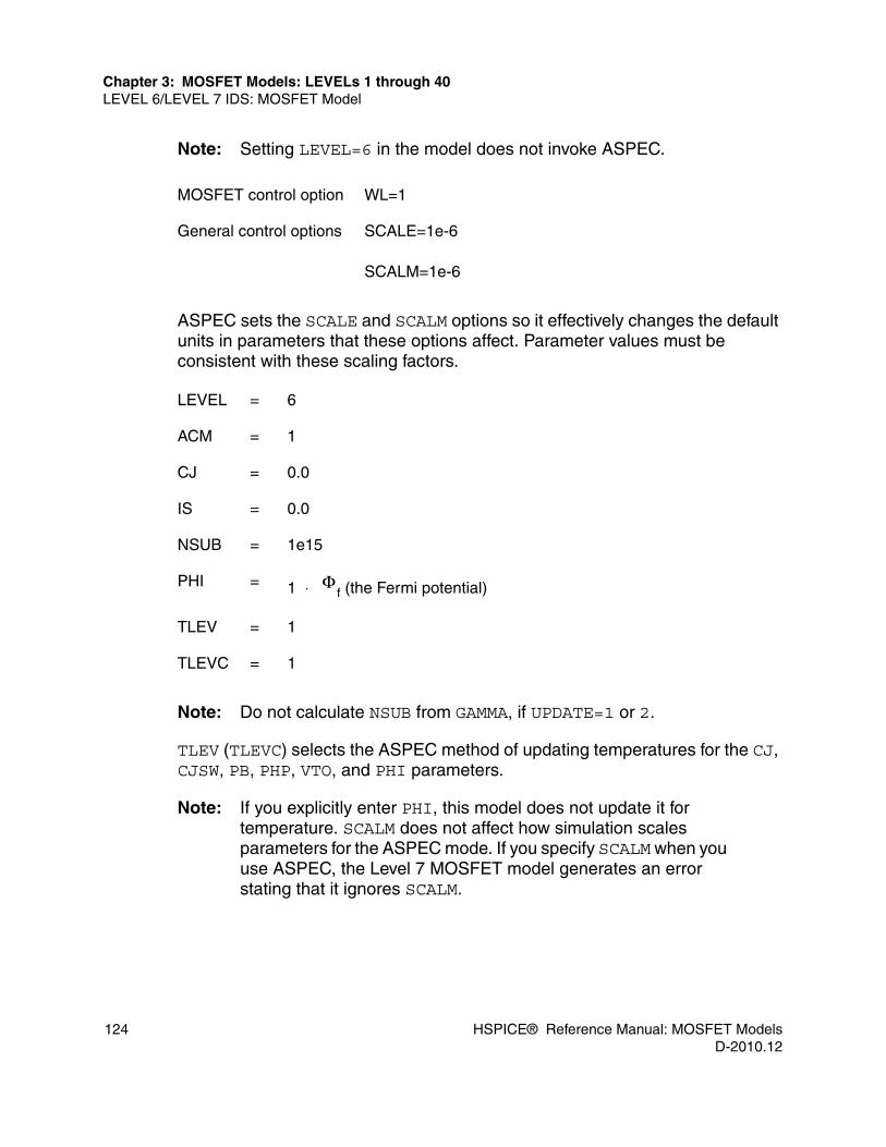
124 HSPICE® Reference Manual: MOSFET ModelsD-2010.12
Chapter 3: MOSFET Models: LEVELs 1 through 40LEVEL 6/LEVEL 7 IDS: MOSFET Model
Note: Setting LEVEL=6 in the model does not invoke ASPEC.
ASPEC sets the SCALE and SCALM options so it effectively changes the default units in parameters that these options affect. Parameter values must be consistent with these scaling factors.
Note: Do not calculate NSUB from GAMMA, if UPDATE=1 or 2.
TLEV (TLEVC) selects the ASPEC method of updating temperatures for the CJ, CJSW, PB, PHP, VTO, and PHI parameters.
Note: If you explicitly enter PHI, this model does not update it for temperature. SCALM does not affect how simulation scales parameters for the ASPEC mode. If you specify SCALM when you use ASPEC, the Level 7 MOSFET model generates an error stating that it ignores SCALM.
MOSFET control option WL=1
General control options SCALE=1e-6
SCALM=1e-6
LEVEL = 6
ACM = 1
CJ = 0.0
IS = 0.0
NSUB = 1e15
PHI = 1 ⋅ f (the Fermi potential)
TLEV = 1
TLEVC = 1
Φ

HSPICE® Reference Manual: MOSFET Models 125D-2010.12
Chapter 3: MOSFET Models: LEVELs 1 through 40LEVEL 7 IDS Model
LEVEL 7 IDS Model
The LEVEL 7 model is the same as the LEVEL 6 model except for the PHI value.
If you specify PHI, then:
For LEVEL=6
, where
is the surface potential.
For LEVEL=7
To transform a LEVEL 7 equation to LEVEL 6, make the following substitution:
To transform a LEVEL 6 model into a LEVEL 7 model, make the following substitution:
LEVEL 8 IDS Model
The LEVEL 8 MOSFET model, derived from research at Intersil and General Electric, is an enhanced version of the LEVEL 2 ids equation. LEVEL 2 differs from LEVEL 8 in the following areas:■ effective substrate doping■ threshold voltage■ effective mobility■ channel length modulation■ subthreshold current.
ΦsPHI
2----------= Φs2
Φs PHI=
PHI 2 PHI⋅→
PHI Level 7( ) PHI Level 6( ) 2⁄=

126 HSPICE® Reference Manual: MOSFET ModelsD-2010.12
Chapter 3: MOSFET Models: LEVELs 1 through 40LEVEL 8 IDS Model
LEVEL 8 Model ParametersMOSFET Level 8 uses the generic MOSFET model parameters described in Chapter 2, Common MOSFET Model Parameters. This level also uses the parameters described in this section, which apply only to MOSFET Level 8.
LEVEL 8 Model EquationsThis section lists the LEVEL 8 model equations.
IDS EquationsLEVEL 8 ids equations are the same as in the LEVEL 2 model (see LEVEL 2 Model Equations on page 70).
Effective Channel Length and WidthThe Level 8 model calculates the effective channel length and width from the drawn length and width (see LEVEL 2 Model Equations on page 70).
Effective Substrate Doping, nsubThe SNVB model parameter varies the substrate doping concentration linearly as a function of vsb:
The preceding equation computes γ , φ, and xd parameters for nsub:
Table 23 Channel Length Modulation Parameters, MOSFET Level 8
Name (Alias) Units Default Description
A1 0.2 Channel length modulation exponent (CLM=8)
CLM 7 Channel length modulation equation selector
LAM1 1/m 0.0 Channel length modulation length correction
LAMBDA (LAM, LA) 0.0 Channel length modulation coefficient
nsub NSUB SNVB vsb⋅+=

HSPICE® Reference Manual: MOSFET Models 127D-2010.12
Chapter 3: MOSFET Models: LEVELs 1 through 40LEVEL 8 IDS Model
If SNVB is zero, then γ =GAMMA. You can adjust the γ value for the short-channel effect the same way as in the LEVEL 2 model. NSUB calculates the φ value.
Threshold Voltage, vthETA specifies the threshold voltage reduction due to the potential barrier lowering effect.
Modify γ for the short-channel effect, the same as in the LEVEL 2 model to obtain the effective γ .
Saturation Voltage vdsatLevel 8 computes the vsat saturation voltage the same way as in the LEVEL 2 model. This model includes the carrier velocity effect only if ECRIT is greater than zero.
ECRIT > 0:
The following equation calculates the vc value used in the preceding equation:
ECRIT ≤ 0 or MOB=7:
This model computes vsat as in the LEVEL=2 model (see Saturation Voltage, vdsat on page 71).
γ2 ε si q nsub⋅ ⋅ ⋅
COX---------------------------------------------------=
Φ 2 vt lnnsub
ni------------⎝ ⎠
⎛ ⎞⋅ ⋅=
xd2 ε si⋅
q nsub⋅----------------------=
vbi VTO g ⇒ Φ–8.14e-22 ETA⋅
COX Leff3⋅
---------------------------------------- Þvds– η 1–( ) vsb Φ+( )⋅+=
vth vbi g vsb Φ+⋅+=
vdsat vsat vc vsat2 vc2+–+=
vc ECRIT Leff⋅=
vdsat vsat=

128 HSPICE® Reference Manual: MOSFET ModelsD-2010.12
Chapter 3: MOSFET Models: LEVELs 1 through 40LEVEL 8 IDS Model
Effective Mobility, ueffThe MOB mobility equation selector controls the mobility reduction equations. In the LEVEL 8 model, set MOB to 2, 3, 6, or 7. Default=6.
MOB=2 Mobility Reduction
MOB=3 Mobility Reduction
In the preceding equation, egfet is the silicon energy gap at the analysis temperature:
In the preceding equation, t is the temperature in degrees Kelvin.
If VMAX>1:
MOB=6 Mobility ReductionFor UEXP>0:
If , then
Otherwise,
For UEXP=0:
ueff UOε se UCRIT⋅
COX vgs vth– UTRA ⇒vde–( )⋅-------------------------------------------------------------------------------------
UEXP
⋅=
ueffUO
12.1e-8 vgs vth egfet Φ–+ +( )⋅
6 TOX⋅--------------------------------------------------------------------------------+
-----------------------------------------------------------------------------------------=
egfet 1.167.02e-4 t2⋅
t 1108+------------------------------–=
ueff
ueff
1ueff
VMAX Leff⋅-------------------------------- vde⋅+
----------------------------------------------------------=
vgs vth–( )ε si UCRIT⋅
COX--------------------------------> ueff
UOε si UCRIT⋅
COX vgs vth–( )⋅-----------------------------------------------
UEXP
⋅
1UTRA
Leff---------------- vde⋅+
----------------------------------------------------------------------------------=
ueffUO
1UTRA
Leff---------------- vde⋅+
------------------------------------------=

HSPICE® Reference Manual: MOSFET Models 129D-2010.12
Chapter 3: MOSFET Models: LEVELs 1 through 40LEVEL 8 IDS Model
UCRIT for UEXP=0 has a dimension of (1/V).
MOB=7 Mobility Reduction
The following equation calculates the body value used in the preceding equation:
Channel Length ModulationThe CLM equation selector controls the channel length modulation equations. In the LEVEL 8 model, set CLM to 6, 7, or 8. Default=7.
CLM=6 SPICE Channel Length ModulationIf LAMBDA=0:
Otherwise, . Then:
Note: The LEVEL 2 model has no LAM1 term.
This model modifies the current for the channel length modulation effect in the entire regions:
CLM=7 Intersil Channel Length ModulationIf CLM=7, this model computes ΔL only for the saturation region.
ueffUO
1 UCRIT vgs vth–( )⋅+[ ] 1UTRA
Leff---------------- vde⋅+⎝ ⎠
⎛ ⎞⋅--------------------------------------------------------------------------------------------------------------------------=
ueffUO
1 UTRA vgs vbi– η⇒vde2
---------–bodyvde
------------+⎝ ⎠⎛ ⎞⋅+
-------------------------------------------------------------------------------------------------------=
body23--- γ vde vsb Φ+ +( )3 2/ vsb Φ+( )3 2/–[ ]⋅ ⋅=
λ xdleff vds⋅------------------------ vds vdsat–
4---------------------------- 1
vds vdsat–4
----------------------------⎝ ⎠⎛ ⎞ 2
++⋅=
λ LAMBDA= ΔLλ Leff vds⋅ ⋅
1 LAM1 Leff⋅+-----------------------------------------=
idsids
1ΔLLeff--------–
-----------------=

130 HSPICE® Reference Manual: MOSFET ModelsD-2010.12
Chapter 3: MOSFET Models: LEVELs 1 through 40LEVEL 8 IDS Model
vds > vdsat
CLM=8 If CLM=8, this model computes ΔL only for the saturation region.
vds > vdsat
Subthreshold Current IdsThe LEVEL 8 model has different subthreshold current equations, depending on the value of the CAV model parameter.
Define:
For CAV ≠ 0
Subthreshold Region, vgs < von
If vgs>vth:
If vgs≤vth
ΔLLAMBDA Leff⋅1 LAM1 Leff⋅+----------------------------------------- vds vdsat–( )⋅=
idsids
LΔLLeff--------–
------------------=
ΔLLeff
11 LAM1 Leff⋅+( ) 1 vde+( )A1⋅
LAMBDA vds vde–( )⋅----------------------------------------------------------------------------------+
-------------------------------------------------------------------------------------------=
idsids
1ΔLLeff--------–
-----------------=
fast vt η q NFS⋅COX
--------------------- γ2 vsb Φ+( )1 2/⋅----------------------------------------
ε si q SNVB vsb Φ+⋅ ⋅ ⋅γ COX2⋅
---------------------------------------------------------------------+ + +⋅=
von vth CAV fast⋅+=
ids ids von vde vsb, ,( ) e1–
CAV2
------------–⎝ ⎠⎛ ⎞
e
1fast--------- CAV 2–( ) vgs vth–( )⋅
2 CAV2 fast2⋅ ⋅------------------------------------------------------------– vgs vth–( )
⎩ ⎭⎨ ⎬⎧ ⎫
⋅ ⋅=

HSPICE® Reference Manual: MOSFET Models 131D-2010.12
Chapter 3: MOSFET Models: LEVELs 1 through 40LEVEL 27 SOSFET Model
For CAV=0
If CLM=8:
Otherwise,
Subthreshold Region, vgs<von
If WIC=3, the next equation calculates the ids subthreshold current:
N0eff and NDeff are functions of effective device width and length.
LEVEL 27 SOSFET Model
MOSFET Level 27 is a three-terminal silicon-on-sapphire (SOS) FET transistor model.[4] This SOSFET model is based on a sapphire insulator that isolates the substrate and models the behavior of SOS devices more accurately than standard MOSFET models with physically unreal parameter values. The SOSFET model also includes a charge conservation model (based on the Ward and Dutton model).
Because the defaults of the SOSFET model parameters depend on the channel length, you must specify the SOSLEV model parameter to select either the 5 μm or 3 μm processing model.
SOSLEV=1 selects the 5 μm model; otherwise, this model automatically uses the 3 μm value, including the second-order effects (default=3 μm).
Note: This model does not include bulk nodes. If you specify bulk nodes, simulation ignores them.
This model does not use the ACM model parameter, because it does not include any junction diodes. Also, the only value that the CAPOP model parameter accepts is 7. Seven is its own charge conservation model, which you cannot use in other MOSFET models.
ids ids von vde vsb, ,( ) e1–
CAV2
------------–⎝ ⎠⎛ ⎞
evgs vth–
fast----------------------⎝ ⎠
⎛ ⎞⋅ ⋅=
von vth 3 fast⋅+=
von vth 2 fast⋅+=
ids ids von vde vsb, ,( ) evgs von–
fast------------------------⎝ ⎠
⎛ ⎞⋅=
ids ids vgs vde vsb, ,( ) isub N0eff NDeff vgs vds, , ,( )+=

132 HSPICE® Reference Manual: MOSFET ModelsD-2010.12
Chapter 3: MOSFET Models: LEVELs 1 through 40LEVEL 27 SOSFET Model
Temperature compensation equations for the VTO and UO SOSFET model parameters are the same as those in the MOSFET model.
Note: This model includes a special option for bulk nodes for silicon on sapphire. In the model definition, if you specify -1 for the bulk node, this model generates a special node for each element. This bulk node is named in the form, B#<element_name>, where the element name is the name of the defined element. Use this name in any statement, such as a .PRINT statement to refer to the bulk node in the element.
Syntax.MODEL mname PMOS <LEVEL=27> <SOSLEV=val> <pname1=val1>.MODEL mname NMOS <LEVEL=27> <SOSLEV=val> <pname=val1>
You can use this .MODEL syntax to include a MOSFET Level 27 model in your HSPICE netlist. For a general description of the .MODEL statement, see the HSPICE Reference Manual: Commands and Control Options.
Parameter Description
mname Model name.
PMOS Identifies a p-channel MOSFET model.
NMOS Identifies an n-channel MOSFET model.
LEVEL Model level selector.
SOSLEV Selects the processing model. If you set SOSLEV=1, the default=5μm. The automatic default=3μm.
pname Parameter model.

HSPICE® Reference Manual: MOSFET Models 133D-2010.12
Chapter 3: MOSFET Models: LEVELs 1 through 40LEVEL 27 SOSFET Model
LEVEL 27 Model ParametersTable 24 5-μm Model Parameters
Name (Alias) Units Default Description
CGDO F/m Gate-drain overlap capacitance per unit channel width. Default=3.1e-10 (n-type), 2.2e-10 (p-type).
CGSO F/m Gate-source overlap capacitance per unit channel width. Default=3.1e-10 (n-type), 2.2e-10 (p-type).
LD m Lateral diffusion. The default=0.6μ (n- type), 0.3μ (p-type).
RSH ohm/sq Drain and source diffusion sheet resistance. The default=25 (n¦-type), 100 (p-type).
SOSLEV 1 Model index.
TOX m 7.0e-8 Oxide thickness.
UO cm2/(V⋅ s) Surface mobility. Default=350 (n-type), 220 (p-type).
VTO V Threshold voltage. Default=1.25 (n-type), -1.25 (p-type).
Table 25 3-μm Model Parameters
Name (Alias) Units Default Description
A m/V 0.1μm Channel length shortening coefficient (2nd effect)
ALPHA V/m Threshold voltage length dependence. Default=0.15μ (n-type), 0.18μ (p-type).
CAPOP 7 Capacitance model selector.

134 HSPICE® Reference Manual: MOSFET ModelsD-2010.12
Chapter 3: MOSFET Models: LEVELs 1 through 40LEVEL 27 SOSFET Model
ExampleThis example is based on demonstration netlist m127iv.sp, which is available in directory $<installdir>/demo/hspice/mos:
CGDO F/m Gate-drain overlap capacitance per unit channel width. Default=4.6e-10 (n-type), 3.6e-10 (p-type).
CGSO F/m Gate-source overlap capacitance per unit channel width. The default=4.6e-10 (n-type), 3.6e-10 (p-type).
EC V/m Critical electric field for velocity saturation (2nd effect). The default=3.0e6 (n-type), 7.5e6 (p-type).
FB Body effect coefficient (2nd effect). Default=0.15 (n-type), 0 (p-type).
LD m Lateral diffusion. Default=0.3μ (n-type), 0.2μ (p-type).
LEVEL 27 Model level selector.
RSH ohm/sq Drain and source diffusion sheet resistance. Default=25 (n-type), 80 (p-type).
SOSLEV 2 Model index.
THETA 1/V Mobility degradation coefficient (2nd effect). Default=0.055 (n-type), 0.075 (p-type).
TOX m 3.4e-8 Oxide thickness.
UO cm2/(V⋅ s) Surface mobility. Default=370 (n-type), 215 (p-type).
VTO V Threshold voltage. Default=0.83 (n-type), -0.74 (p-type).
Table 25 3-μm Model Parameters
Name (Alias) Units Default Description

HSPICE® Reference Manual: MOSFET Models 135D-2010.12
Chapter 3: MOSFET Models: LEVELs 1 through 40LEVEL 27 SOSFET Model
*file: ml27iv.sp ids and vgs curves for nmos and pmos sosfets.*mosfet level=27 p and n
.options acct list nopage nomod post
.op
.dc vddn 0 5.0 .1
* n-channel ids curves (vd=0-<<5, vg=1,2,3,4,5).print dc i(vn1) i(vn2) i(vn3) i(vn4) i(vn5).probe dc i(vn1) i(vn2) i(vn3) i(vn4) i(vn5)
* p-channel ids curves (vd=0-<<-5,vg=-1,-2,-3,-4,-5).print dc i(vp1) i(vp2) i(vp3) i(vp4) i(vp5).probe dc i(vp1) i(vp2) i(vp3) i(vp4) i(vp5)
* v g s curves.print dc i(vn6) i(vp6).probe dc i(vn6) i(vp6)
* n-channel lx7=gm(vd=5, vg=0-<<5, vs=0)* n-channel lx8=gd (vd=0-<<5, vg=5, vs=0)* n-channel lx9=gb (vd=5, vg=5, vs=0).print dc lx7 (m21) lx8(m5) lx9(m31)
* p-channel lx7=gm (vd=0, vg=0-<<-5, vs=-5)* p-channel lx8=gd (vd=0-<<-5, vg=-5, vs=-5)* p-channel lx9=gb (vd=0, vg=0, vs=-5).print dc lx7(m22) lx8(m15) lx9(m32)*vddn 99 0 5.0epd 98 0 99 0 -1
v1 1 0 1v2 2 0 2v3 3 0 3v4 4 0 4v5 5 0 5v11 11 0 -1v12 12 0 -2v13 13 0 -3v14 14 0 -4v15 15 0 -5*vn1 99 31 0vn2 99 32 0vn3 99 33 0vn4 99 34 0vn5 99 35 0

136 HSPICE® Reference Manual: MOSFET ModelsD-2010.12
Chapter 3: MOSFET Models: LEVELs 1 through 40LEVEL 27 SOSFET Model
m1 31 1 0 n1 8u 8um2 32 2 0 n1 8u 8um3 33 3 0 n1 8u 8um4 34 4 0 n1 8u 8um5 35 5 0 n1 8u 8u*vp1 98 41 0vp2 98 42 0vp3 98 43 0vp4 98 44 0vp5 98 45 0
m11 41 11 0 p1 8u 8um12 42 12 0 p1 8u 8um13 43 13 0 p1 8u 8um14 44 14 0 p1 8u 8um15 45 15 0 p1 8u 8u** g m testvn6 5 36 0vp6 0 46 0m21 36 99 0 n1 8u 8um22 46 98 15 p1 8u 8u** g m b testvn7 5 37 0vp7 0 47 0m31 37 5 0 98 n1 8u 8um32 47 0 15 99 p1 8u 8u*.model n1 nmos level=27 soslev=2+vto=0.814 tox=0.34e-7 theta=0.55e-1+fb=0.15 ec=0.3e7 a=0.1e-6+uo=370 cgso=0.46e-9 cgdo=0.46e-9+rsh=25 ld=0.3e-6*.model p1 pmos level=27 soslev=2+vto=-0.7212 tox=0.34e-7 theta=0.75e-1+fb=0.0 ec=0.75e7 a=0.1e-6+uo=215 cgso=0.36e-9 cgdo=0.36e-9+rsh=80 ld=0.2e-6*.end

HSPICE® Reference Manual: MOSFET Models 137D-2010.12
Chapter 3: MOSFET Models: LEVELs 1 through 40LEVEL 27 SOSFET Model
Non-Fully Depleted SOI ModelSeveral MOSFET models are currently available for SOS/SOI applications. The 3-terminal SOS model (LEVEL=27) is stable for circuit design usage, but has some limitations. This model does not provide for depleted bulk. Use it only with applications that are not fully depleted and that do not consider kink effects.
The following circuit example is a 4-terminal SOI model for incompletely depleted bulk with the kink effect. Its sub-circuit allows a parasitic capacitance to the substrate. In this example, the bulk is the region under the channel. This model assumes that the substrate is the conductive layer under the insulator.■ For SOI, the insulator is usually silicon dioxide and the substrate is silicon. ■ For SOS, the insulator is sapphire and the substrate is the metal that
contacts the back of the integrated circuit die.
Model ComponentsThis model consists of the following subcomponents:■ Core IDS model: any level works because the impact ionization and weak
inversion models are common to all DC levels. The example uses a LEVEL=3 DC MOS model.
■ Subthreshold model: the WIC=3 model parameter allows the older models to use the more advanced models found in the BSIM (LEVEL=13, LEVEL=28) models. The N0 model parameter should have a typical value around 1.0.
■ Impact ionization model: set ALPHA and VCR parameters to enable the impact ionization model, which is available to all MOS DC equations. Typical values are ALPHA=0.1 and VCR=18.
■ Charge conservation gate cap model (CAPOP=9, XQC=.4) prevents the floating bulk node from obtaining extreme values.
■ The automatic periphery diode area calculation method (ACM) is set to 3 to automatically calculate the source and drain resistances and diode junction leakage, and the capacitance. (ACM=3 CJ=0 CJSW=0 CJGATE=4e-10 JS=0 JSW=1e-9 LD=.1u HDIF=1.5u RS=40 RD=40 N=1).
Note: These models assume that the source/drain diffusions extend to the buried oxide. The area part of the diode has no capacitance to bulk. However, the subcircuit includes linear capacitors to the substrate.

138 HSPICE® Reference Manual: MOSFET ModelsD-2010.12
Chapter 3: MOSFET Models: LEVELs 1 through 40LEVEL 27 SOSFET Model
Obtaining Model ParametersUse the optimizing capabilities in the Level 27 MOSFET model to obtain the core IDS model parameters.
Use the optimizer to obtain the core model, subthreshold, and impact ionization parameters. The subthreshold model selected is an improved BSIM type of model that was altered for the older models. The charge conservation model is more charge conserving than the original Ward-Dutton model in SPICE 2G6.
Calculating the automatic diode area and the resistance estimates the junction capacitance, saturation current, and resistance as a function of the transistor width. Use the VNDS and NDS parameters for a piecewise linear approximation to reverse the junction current characteristics.
Figure 7 Non Fully Depleted SOI Model
ExampleThis example is based on demonstration netlist ssoi.sp, which is available in directory $<installdir>/demo/hspice/mos:
source drain
gate
Insulator
IsolationIsolation
Silicon/Substrate

HSPICE® Reference Manual: MOSFET Models 139D-2010.12
Chapter 3: MOSFET Models: LEVELs 1 through 40LEVEL 27 SOSFET Model
ssoi.sp LEVEL=3 floating bulk model** non-fully depleted* test 1st order soi model with floating substrate.option nomod post* substrate capacitance 3.45e-11 is for SiO2.param t_sub_ox=.5u subcap='3.45e-11/t_sub_ox' hdif=1.5u.global substrate.dc vd 0 5 0.1 sweep vg 1.5 3.5 0.5.print id=i(xm1.m) vds=v(d) vgs=v(g).param vds=0 vgs=0 vbs=0vd d gnd vdsvg g gnd vgsvs s gnd 0vsub substrate gnd vbsxm1 d g s nch w=50u L=5u.macro nch d g s w=10u l=2u* macro definition for fet+ parasitic cap to substrate* assumes existence of undepleted bulkm d g s b nch w=w L=Lcx1 d substrate c='w*2*hdif*subcap'cx2 s substrate c='w*2*hdif*subcap'cx3 b substrate c='w*L*subcap'.eom.model nch nmos LEVEL=3+ lmin=.5u lmax=100u wmin=.5u wmax=500u $model selector+ ld=0.1u wd=.15u xl=0 xw=0$diffusion+photobias+ acm=3 hdif=hdif rsh=30 rs=10k rd=10k $resistors+ ldif=0.1u$junction cap (ACM=3 (h9007 only) allows diode on gate edge+ cj=0 cjsw=0 cgate=0.4e-9 mjsw=0.33 php=0.6+ js=0 jsw=1e-9 n=1 vnds=.5 nds=1 $junction leakage+ bex=-1.5 tcv=2m $temperature+ tox=200 capop=9 xqc=.4 meto=0.08u $gate cap+ alpha=0.1 vcr=18 $impact ionization+ vto=0.7 phi=1 gamma=1 $threshold+ eta=10 xj=0.1u $threshold+ wic=3 n0=0.9 nd=0 $subthreshold+ uo=400 theta=1m $dc mobility+ vmax=100k kappa=0 $dc saturation.end

140 HSPICE® Reference Manual: MOSFET ModelsD-2010.12
Chapter 3: MOSFET Models: LEVELs 1 through 40LEVEL 27 SOSFET Model
Figure 8 LEVEL 3 Floating Bulk Model
Fully Depleted SOI Model ConsiderationsFully depleted transistors require additional modeling equations. The first-order effects are:■ Threshold sensitivity to the substrate.■ No kink current.■ Silicon thickness limits the minimum depletion capacitance.
Lack of these effects does not seriously affect an inverter, because the source-to-substrate voltage does not move. Digital circuits with good gate drive are not seriously affected, because a large gate voltage renders a small Vth shift to a small change in the IDS current.
1
2
3
4

HSPICE® Reference Manual: MOSFET Models 141D-2010.12
Chapter 3: MOSFET Models: LEVELs 1 through 40LEVEL 38 IDS: Cypress Depletion Model
The substrate threshold sensitivity can affect circuits such as analog amplifiers that include transistors at back-bias and low gate voltages.
LEVEL 38 IDS: Cypress Depletion Model
The LEVEL 38 Cypress Depletion MOSFET model (Cypress Semiconductor Corporation) is a further development of the Synopsys Level 5 MOSFET device model. Level 38 features:■ BSIM-style length and width sensitivities■ Degraded body effect at high substrate bias (second GAMMA)■ Empirical fitting parameters for Ids current calculations in the depletion
mode of operations■ A comprehensive surface mobility equation■ Drain-induced barrier lowering
At the default parameter settings, the LEVEL 38 model is basically backwards-compatible with LEVEL 5 /ZENH=0.0 with the exception of the surface mobility degradation equation (see the discussion on the next page). Refer to the documentation for LEVEL 5 for the underlying physics that forms the foundation for the Huang-Taylor construct.
In LEVEL 38, the temperature compensation for threshold is ASPEC-style, concurring with the default in LEVEL 5. This section describes the model parameters that are unique to this depletion model. It also describes additional temperature compensation parameters.
LEVEL 38 lets you use all Synopsys device model capacitance options (CAPOP). CAPOP=2 is the default setting for LEVEL 38. If you set CAPOP=6 (AMI capacitance model), LEVEL 38 capacitance calculations become identical to those of LEVEL 5.
The ACM default parameter (ACM=0 in LEVEL 38) invokes SPICE-style parasitics. You can set ACM to 1 (ASPEC), or to 2 (Synopsys device model). All MOSFET models follow this convention.
You can use .OPTION SCALE with the LEVEL 5 MOSFET device model. However, you cannot use the SCALM option, due to the difference in units. You also cannot use the DERIV option.
You must specify the following parameters for MOS LEVEL 38: VTO (VT), TOX, UO (UB), FRC, ECV, and NSUB (DNB).

142 HSPICE® Reference Manual: MOSFET ModelsD-2010.12
Chapter 3: MOSFET Models: LEVELs 1 through 40LEVEL 38 IDS: Cypress Depletion Model
As with LEVEL 5, this model calculates the Ids current according to three gate voltage regions:■ Depletion Region, vgs - vfb < 0
The low gate voltage region, which the bulk channel dominates.■ Enhancement Region, vgs - vfb > 0, vds < vgs - vfb
The region defined by high gate voltage and low drain voltage. In the enhancement region, both channels are fully turned on.
■ Partial enhancement region, vgs - vfb > 0, vds > vgs - vfb
This region has high gate and drain voltages so the surface region is partially turned on, and the bulk region is fully turned on.
To better model depletion region operations, empirical fitting constants have been added to the original Huang-Taylor mechanism to account for the effects caused by nonuniform channel implants and also to make up for an oversight in the average capacitance construct[5]. The enhancement region uses a significantly more elaborate surface mobility model.
Body effect in LEVEL 38 is calculated in two regions[6].■ Bulk body effect, vsb-vsbc > 0
With sufficiently high (and negative) substrate bias (exceeding vsbc), the depletion region at the implanted channel-substrate junction reaches the Si-oxide interface. Under such circumstances, the free carriers can accumulate only at the interface (as in an enhancement device) and the bulk doping level determines the body effect.
■ Implant-dominated body effect, vsb-vsbc < 0
Before reaching vsbc, and as long as the implant dose overwhelms the substrate doping level, the deeply-buried transistor (due to the implant) dominates the body effect of the depletion mode device. The γ body effect coefficient is proportional to both the substrate doping and to the first-order implant depth. In Level 38, the BetaGam empirical parameter amplifies the body effect due to deep implant.
Model parameters that start with L or W represent geometric sensitivities. In the model equations, three model parameters determine the zX quantity (X is the variable name):
• Large-and-wide channel case value (X).
• Length sensitivity (LX).
• Width sensitivity (WX).

HSPICE® Reference Manual: MOSFET Models 143D-2010.12
Chapter 3: MOSFET Models: LEVELs 1 through 40LEVEL 38 IDS: Cypress Depletion Model
The model calculates these parameters according to zX=X+LX/Leff+WX/Weff. For example, the following equation calculates the zero field surface mobility:
Note: This model uses mostly micrometer units rather than meter units. Units and defaults are often unique in LEVEL 38. The finite difference method calculates the Ids derivatives that define the gm, gds, and gmbs small signal gains. This model does not use the SCALM and DERIV options.
LEVEL 38 Model ParametersMOSFET Level 38 uses the generic MOSFET model parameters described in Chapter 2, Common MOSFET Model Parameters. This level also uses the parameters described in this section, which apply only to MOSFET Level 38.
LEVEL 38 Model Equations
IDS EquationsDepletion, vgs-vfb <0
Table 26 Capacitance Parameters
Name (Alias) Units Default Description
AFC 1.0 Area factor for MOSFET capacitance
CAPOP 6 Gate capacitance selector
METO μm 0.0 Metal overlap on gate
zUO UOLUOleff
------------ WUOweff
--------------+ +=
ids β1 q zKI0⋅⎩⎨⎧ NI vde cav vgs vfb–( ) vde
vde2
2-----------–⋅⋅+⋅ ⋅ ⋅=

144 HSPICE® Reference Manual: MOSFET ModelsD-2010.12
Chapter 3: MOSFET Models: LEVELs 1 through 40LEVEL 38 IDS: Cypress Depletion Model
Enhancement, vgs-vfb vde >0
Partial Enhancement, vgs-vfb<vde
The following equations calculate values used in the preceding equations:
,
,
,
The temperature dependence of the mobility terms assume the ordinary exponential form:
23---– cav γ vde vsb Phid+ +( )3 2/ vsb Phid+( )3 2/–[ ] Icrit+
⎭⎬⎫⋅ ⋅ ⋅
ids β1 q zKI0 NI vde23--- ⇒cav ⇒γ ⇒ vde vsb Phid+ +( )3 2/
vsb Phid+( )3 2/–
[
]
–
Icrit+
⋅ ⋅ ⋅⎩
⎭
⎨
⎬
⎧
⎫ β vgs vfb–( ) vdevde2
2-----------–⋅⋅+
⋅=
ids β1 q zKI0 NI vde cav vgs vfb–( ) vdevde2
2-----------–⋅⋅+⋅ ⋅ ⋅
⎩⎨⎧⋅=
23---– cav γ vde vsb Phid+ +( )3 2/ vsb Phid+( )3 2/–[ ] Icrit+⋅ ⋅ ⋅
⎭⎬⎫
12---β 1
2---β1 ⇒cav–⎝ ⎠
⎛ ⎞ vgs vfb–( )2⋅
β1zKBeta1
1 UHSATvdeLeff----------⋅+
----------------------------------------------- U⋅ HWeffLeff------------⋅=
β UBeff coxWeffLeff------------⋅ ⋅= cav
cox cs⋅cox cs+---------------------=
csKCS ε Si⋅DP 1e-4⋅---------------------------= Phid vt ln
DNB nd⋅ni2
--------------------------⎝ ⎠⎛ ⎞⋅=
ndNI 1e4⋅
DP-----------------------= vde min vds vdsat,( )=

HSPICE® Reference Manual: MOSFET Models 145D-2010.12
Chapter 3: MOSFET Models: LEVELs 1 through 40LEVEL 38 IDS: Cypress Depletion Model
The following equation calculates the continuity term at the body effect transition point:
This model uses the preceding equation if vsb>vsbc. Otherwise,
The following sections describe saturation voltage, threshold voltage, body effect transition voltage, and the γ body effect coefficient.
Threshold Voltage, vthThe VTO model parameter, often called the “pinch-off,” is a zero-bias threshold voltage extrapolated from a large device operating in the depletion mode. The following equation calculates the effective pinch-off threshold voltage, including the device size effects and the terminal voltages:
The following equations calculate values used in the preceding equation:
for vsb > vsbc; 0 otherwise.
,
,
UH t( ) UH tnom( ) ttnom-------------⎝ ⎠
⎛ ⎞ TUH⋅=
zUO t( ) zUO tnom( ) ttnom-------------⎝ ⎠
⎛ ⎞ TUH⋅=
Icrit23--- cav vde vsbc Phid+ +( )3 2/ vsbc Phid+( )3 2/–[ ] γ 1
zBetaGam--------------------------- 1–⎝ ⎠
⎛ ⎞⋅ ⋅ ⋅⋅–=
Icrit 0=
vth vfb βd ⇒vch γ ⇒Phid vsb+( )1 2/– vcrit+[ ]–=
vfb zVTO zETA ⇒– vds βd vch γ 0 ⇒Phid1 2/–( )⋅+=
vcrit γ γzBetaGam---------------------------–⎝ ⎠
⎛ ⎞ ⇒Phid vsbc+( )1 2/=
βdUH cav⋅zUO cox⋅----------------------------= vch
q NI⋅cav
----------------=
γ 02 ε si q na1⋅ ⋅ ⋅( )1 2/
cav---------------------------------------------------------=
na1nd DNB⋅nd DNB+--------------------------= nd
NIDP 1e-4⋅---------------------------=

146 HSPICE® Reference Manual: MOSFET ModelsD-2010.12
Chapter 3: MOSFET Models: LEVELs 1 through 40LEVEL 38 IDS: Cypress Depletion Model
The following equation computes the effective γ , including small device size
effects: for vsb>vsbc, and =g; otherwise,
The following equations calculate values used in the preceding equations:
If SCM ≤0, then ; otherwise,
If NWM ≤0, then ; otherwise,
This equation calculates the xd value used in the preceding equation:
The following equation calculates the body effect transition point:
If vgs ≤ vth, this model inverts the surface and includes a residual DC current. If vsb is large enough to make vth > vinth, then vth is the inversion threshold voltage.
To determine the residual current, simulation inserts vinth into the ids, vsat, and mobility equation in place of vgs (except for vgs in the exponential term of the subthreshold current). The following equation computes the inversion threshold voltage (vinth) at a specified vsb:
Saturation Voltage, vdsatThis equation determines the vsat saturation voltage:
γ γzBetaGam---------------------------=
γ γ 0 1 scf–( ) 1 ncf+( )⋅ ⋅=
scf 0=
scfXJ
Leff---------- 1
2xdXJ--------- SCM vds vsb Phid+ +⋅( )1 2/⋅+
1 2/1–
⎩ ⎭⎨ ⎬⎧ ⎫
⋅=
ncf 0=
ncfNWM xd Phid( )1 2/⋅ ⋅
Weff-----------------------------------------------------------=
xd2 ε si⋅
q DNB⋅-----------------------⎝ ⎠
⎛ ⎞ 1 2/=
VsbcqDP2
2ε si-------------- NI
DP 1e 4–⋅------------------------------ DNB–⎝ ⎠
⎛ ⎞ zDVSBC TDVSBC ⇒t tnom–( ) Phid–+ +=
vinth vfbq NI⋅
cox----------------– vsb– DVIN zETA ⇒– vds+=

HSPICE® Reference Manual: MOSFET Models 147D-2010.12
Chapter 3: MOSFET Models: LEVELs 1 through 40LEVEL 38 IDS: Cypress Depletion Model
Simulation modifies vsat to include the carrier velocity saturation:
The following equation calculates the vc value used in the preceding equation:
Mobility Reduction, UBeffThe UB surface mobility depends on the terminal voltages:
The following equations calculate Le for the preceding equation:
Linear region
Saturation region
At elevated temperatures, the following equation calculates the zFRC value used in the preceding equation:
ΔL is the channel length modulation effect, defined in the next section. vfb assumes the role of vth in the LEVEL 5 mobility equation. The degradation parameters are semi-empirical, and are grouped according to their (linearized) mathematical dependencies instead of their physical origin to better provide parameter extraction.[7]
vsat vgs vfb– vchγ 2
2------ 1 1
4γ 2------ vgs vfb– vch vsb Phid+ + +( )⋅+
1 2/–
⎩ ⎭⎨ ⎬⎧ ⎫
⋅+ +=
vdsat vsat=
vdsat vsat vc vsat2 vc2+( )1 2/–+=
vc ECV Leff⋅=
UBeff1
1zUO----------- zFRC zVFRC vde⋅ zBFRC vsb⋅+ +( ) vgs vfb–( )⋅
TOX----------------------------------------------------------------------------------------------------------------------------------------- vde
VST Le⋅------------------------ zFSB vsb1 2/⋅+ + +
-------------------------------------------------------------------------------------------------------------------------------------------------------------------------------------------------------------------------------------=
Le Leff=
Le Leff ΔL–=
zFRC t( ) zFRC tnom( ) ttnom-------------⎝ ⎠
⎛ ⎞ FRCEX⋅=

148 HSPICE® Reference Manual: MOSFET ModelsD-2010.12
Chapter 3: MOSFET Models: LEVELs 1 through 40LEVEL 38 IDS: Cypress Depletion Model
Channel Length Modulation To include the channel length modulation, modify the ids current:
The following equation calculates ΔL for the preceding equation:
ΔL is in microns, if XJ is in microns and na1 is in cm-3.
Subthreshold Current, idsIf device leakage currents become important for operation near or below the normal threshold voltage, the model considers the subthreshold characteristics. In the presence of surface states, this equation determines the effective threshold voltage (von):
The following equation calculates the fast value used in the preceding equation:
If vgs <von, then:
Partial Enhancement, 0< vgs-vfb < vde
idsids
1ΔL
Leff----------–
-------------------=
ΔL 1e42.73e3 XJ⋅
na1 ln1e20na1------------⎝ ⎠
⎛ ⎞⋅----------------------------------------
1 3/
vds vdsat– PHI+( )1 3/ PHI1 3/–[ ]⋅ ⋅=
von max vth vinth( , ) fast+=
fast vt 1q FSS⋅
cox-------------------- γ
2 Phid vsb+( )1 2/⋅-------------------------------------------------+ +⋅=
ids β1 q zKI0 NI vde cav von vfb–( ) vdevde2
2-----------–⋅⋅+⋅ ⋅ ⋅
⎩⎨⎧⋅=
23---– cav γ vde vsb Phid+ +( )3 2/ vsb Phid+( )3 2/–[ ] Icrit+
⎭⎬⎫
⋅ ⋅ ⋅
12--- β e
vgs von–fast
------------------------⋅ β1 ⇒cav–⎝ ⎠
⎛ ⎞ von vfb–( )2⋅ ⋅+

HSPICE® Reference Manual: MOSFET Models 149D-2010.12
Chapter 3: MOSFET Models: LEVELs 1 through 40LEVEL 38 IDS: Cypress Depletion Model
Full Enhancement, vgs-vfb -vde > 0
Depletion, vgs-vfb < 0
Example Model File$ file Depstor.mod
.MODEL DEPSTOR NMOS LEVEL=38* PARASITIC ELEMENTS+ ACM=1+ LD=0.15u WD=0.2u $ for LEFF AND WEFF+ CJ=0.3E-16 MJ=0.4 PB=0.8 JS=2.0E-17 $ INTRINSIC DIODE+ CJSW=0 MJSW=0.3+ BULK=98 $ DEFAULT NODE FOR SUBSTRATE* THRESHOLD+ VTO=-2.5 LVT=-0.25 WVT=0+ leta=0.02 eta=0.0 weta=0.0+ TCV=0.003 $ TEMPERATURE COEFFICIENT* MISC+ DVIN=0.5 PHI=0.75+ NFS=2e10 DNB=3.0E16
Mobility Model+ UH=1300
+ UO=495 FRC=0.020 FSB=5e-5 VFRC=-1e-4 BFRC=-0+ LUO=-100 LFRC=.03 LFSB=-1e-5 LVFRC=-.002 LBFRC=-1e-3
ids β1 q zKI0 NI vde23--- ⇒cav ⇒γ ⇒ vde vsb Phid+ +( )3 2/ vsb Phid+( )3 2/–[ ]– Ic+⋅ ⋅ ⋅
⎩⎨⎧⋅=
β von vfb–( ) vdevde2
2-----------–⋅ e
vgs von–fast
------------------------⋅ ⋅
ids β1 q zKI0⋅⎩⎨⎧ NI vde cav vgs vfb–( ) vde
vde2
2-----------–⋅⋅+⋅ ⋅ ⋅=
23---– cav γ vde vsb Phid+ +( )3 2/ vsb Phid+( )3 2/–[ ] Icrit+
⎭⎬⎫ e
vgs von–fast
------------------------⋅ ⋅ ⋅ ⋅

150 HSPICE® Reference Manual: MOSFET ModelsD-2010.12
Chapter 3: MOSFET Models: LEVELs 1 through 40LEVEL 40 HP a-Si TFT Model
+ WUO=-30 WFRC=-0.01 WFSB=5e-5 WVFRC=-0.00 + WBFRC=-0.4e-3+ KI0=.9 KBETA1=.5 LKI0=0.16 LKBETA1=-0.15+ WKI0=0.0 WKBETA1=-0.0+ BEX=-1.3 TUH=-1.0 Frcex=1.0
Body Effect+ NWM=0.5 SCM=.1
+ DVSBC=0.1 LDVSBC=0 WDVSBC=0+ TDVSBC=.002+ BetaGam=0.9 LBetaGam=-.2 WBetaGam=.1
Saturation+ ECV= 2.9 VST=8000 UHSAT=0
* CHANNEL LENGTH MODULATION+ XJ=0.1* OXIDE THICKNESS AND CAPACITANCE+ TOX=165 CGSO=0 CAPOP=2* CHANNEL IMPLANT+ NI=1.5e12 KCS=3 DP=0.25*.END
LEVEL 40 HP a-Si TFT Model
The Synopsys Level 40 MOSFET device model represents a Hewlett-Packard amorphous silicon thin-film transistor model.
MOSFET Level 40 uses only the generic MOSFET model parameters described in Chapter 2, Common MOSFET Model Parameters.
Using the HP a-Si TFT ModelTo use the HP a-SI TFT model:
1. Set LEVEL=40 to identify the model as the HP a-Si TFT model.
2. Default value for L is 10μm, and the default value for W is 40 μm.
3. Use the “M” designation for MOSFET rather than the “A” designation for a-Si TFT in the netlist.

HSPICE® Reference Manual: MOSFET Models 151D-2010.12
Chapter 3: MOSFET Models: LEVELs 1 through 40LEVEL 40 HP a-Si TFT Model
4. Use the “NMOS” or “PMOS” designation for device type rather than the “NAT” or “PAT” designation.
Note: Because of the unavailability of p-channel TFTs, PMOS model testing has been limited.
5. LEVEL 40 is a three-terminal model. It lacks bulk nodes so simulation does not append any parasitic drain-bulk or source-bulk diodes to this model. You can specify a fourth node, but it does not affect the simulation results (except for GMIN terms).
6. Parasitic resistances and overlap capacitances are constant. They are not scaled with width, length, and temperature.
7. Capacitance expressions in this model do not conserve charge.
8. The TREF parameter is an exponent in an expression for mobility temperature dependence.
9. Other models use the BEX parameter for similar mobility temperature dependence expressions. The HP a-Si TFT TREF model parameter is not the same as the TREF reference temperature in other models. The reference temperature for the HP a-Si TFT model is 312 K (or 38.85 oC); you cannot modify it. Experimental results from TFT manufacturers indicate that amorphous silicon materials are most stable at this temperature.
10. The default room temperature is 25o C in Synopsys circuit simulators, but is 27o C in most other simulators. When comparing to other simulators, set the nominal simulation temperature to 27o C by using either .TEMP 27 or .OPTION TNOM=27 in the netlist. Although the reference temperature of the HP a-Si TFT model is fixed at 312o K (or 38.85oC), the behavior of the model adjusts to other simulation temperatures that you specify, or that are defaults in Synopsys circuit simulators. In the Level 40 MOSFET model, temperature dependency is enabled.
11. The default CAPOP value is 40, which is the HP a-Si TFT non-charge-conserving capacitance model. CAPOP values of 0, 1, 2, 3, 4, 5, 9, 12, or 13 have not been thoroughly tested.
12. The DERIV default is zero, which selects the analytical method. Set DERIV to 1 to select the finite difference method.

152 HSPICE® Reference Manual: MOSFET ModelsD-2010.12
Chapter 3: MOSFET Models: LEVELs 1 through 40LEVEL 40 HP a-Si TFT Model
Effect of SCALE and SCALM.OPTION SCALE has the same effect for LEVEL 40 as for other Synopsys device models, such as MOSFET Level 3 or Level 28. If you specify the L and W values in microns rather than meters (for example, L=1 rather than L=1m or 1e-6), set .OPTION SCALE=1e-6.
The SCALM option is disabled in the LEVEL 40 model. For standard MOSFET models (such as LEVEL 3), SCALM affects the scale of model parameters such as XL, XW, LD, WD, CJ, and CJSW.
Because the LEVEL 40 model ignores the SCALM option, you can mix LEVEL 40 models in a simulation with other models that use SCALM.
In general, netlists for Synopsys simulators should be as standard as possible. Also, you should convert L and W to meters scale instead of microns scale so that you can use the netlist without .OPTION SCALE=1E-6. If you follow these recommendations, a system-level simulation can use I/O sub-circuits from different vendors.
Noise ModelThe LEVEL 40 model uses the standard NLEV=0 noise model inherited from other Synopsys MOSFET models.
DELVTO ElementYou can use DELVTO and DTEMP on the element line with LEVEL 40.
Device Model and Element Statement Example.MODEL nch nmos LEVEL=40 UO=0.4229 VTO=1.645 PHI=1.25 NSS=0
+ NFS=2.248E+21 VMAX=1231+ THETA=-0.01771 ETA=0.0002703 T1=2.6E-07 T2=0 E1=3.9 E2=0+ GO=9.206E-15 NU=0 K2=2 CHI=0.5+ PSI=1E-20 VTIME=0.01 TREF=1.5 CGSO=5.203E-14 CGDO=4.43E-14+ CSC=0.0001447 RD=5097+ RS=5097 FREQ=1E+06 DEFF=2.15 TAU=1.64E-07 FEFF=0.5MCKT 1 2 3 nch L=1e-05 W=4e-05

HSPICE® Reference Manual: MOSFET Models 153D-2010.12
Chapter 3: MOSFET Models: LEVELs 1 through 40LEVEL 40 HP a-Si TFT Model
LEVEL 40 Model EquationsThe following equations show model parameters in all capital letters; working variables are in lower case. Model parameters and the vgs and vds bias voltages are inputs. Ids, gm, and gds are the DC outputs. The Cgs gate-to-source capacitance and the Cgd gate-to-drain capacitance are the AC outputs. The electron charge is q, the Boltzmann’s constant is k, and the permittivity of a vacuum is ε0.
This model applies the SCALE value before evaluating the equations, and scales by M after evaluation.
and variables are intermediate, not final, quantities.
For a complete description of TFT technology and the device physics underlying these equations, see the Hewlett-Packard HP IC-CAP manual.
Initially, , , , , and .
If , then .
The following equation computes the Cfm dielectric capacitance per unit area:
If and , then
If and , then
If and , then
TEMP is the Synopsys device simulation temperature, specified in οC, but converted to ο K internally to evaluate these equations.
,
If , then and
gmtft gdstft
Cgdi 0= Cgsi 0= phi PHI= vto VTO= uo UO=
uo 0= uo 1=
T1 0≠ T2 0≠ Cfmε 0 E1 E2⋅ ⋅( )
T2 E1⋅( ) T1 E2⋅( )+( )--------------------------------------------------------------=
T1 0= T2 0≠ Cfmε 0 E2⋅( )
T2-------------------------=
T2 0= T1 0≠ Cfmε 0 E1⋅( )
T1-------------------------=
kp uo Cfm 104–⋅ ⋅=
vtk TEMP⋅( )
q-------------------------------=
eg 2 104
TEMP 312–( )⋅ ⋅( ) 1.4+=
vto vto DELVTOmodel type⋅( ) DELVTOelement type⋅( )+ +=
vbi vto= ratioTEMP
312----------------=
VTIME 1≤ uo uo ratioTREF( )⋅= kp kp ratio
TREF( )⋅=

154 HSPICE® Reference Manual: MOSFET ModelsD-2010.12
Chapter 3: MOSFET Models: LEVELs 1 through 40LEVEL 40 HP a-Si TFT Model
Note: TREF is an exponent in adjusting the temperature. It is not the reference temperature of this device model.
(printback definition)
(printback definition)
(printback definition)
If and , then:
If , then:
Cutoff Region (NFS=0, vgs ≤ von)If and , then:
.
Noncutoff Region (NFS ≠ 0)■ If , then .■ If , then .
vfb vto 0.5 PHI⋅( )– 0.5 1.4 eg–( )⋅( )+=
vbi vfb 0.5 PHI ratio⋅+( )+=
vto vbi=
phi phi ratio⋅=
vfb vbi phi–=
vdsat 0=
beta kp W L⋅ ⋅=
vth vbi ETA vds⋅( )+=
NU 0≠ K2 0≠ PSI 0≠ VTIME 1>
vth vth f vgs vds NU K2 PSI CHI VTIME TEMP, , , , , , ,( )+=
von vth=
NFS 0≠
xn 1q NFS 10
4W L⋅ ⋅ ⋅ ⋅( )
Cfm-----------------------------------------------------------------⎝ ⎠
⎛ ⎞+=
von f vth vt xn⋅( ),( )=
NFS 0= vgs von≤
Cgdi 0=
Cgsi 0=
Ids GO f vgs DEFF vds⋅( ),( )⋅=
gm GO= gds GO DEFF⋅=
vgs von> vgsx vgs=
vgs von≤ vgsx von=

HSPICE® Reference Manual: MOSFET Models 155D-2010.12
Chapter 3: MOSFET Models: LEVELs 1 through 40LEVEL 40 HP a-Si TFT Model
Mobility modulation by vgs:
If , then:
is the series combination of the dielectric and space charge capacitance for the MIS structure.
If vds < vdsat, then:
is the effective equivalent dielectric constant of the insulator layers.
Otherwise, :
If , then
Normalized drain current:
ueff f uo η vgs THETA, , ,( )=
VMAX 0>
vdscL VMAX⋅
ueff---------------------------=
vdsat vgsx vth–( ) vdsc vgsx vth–( )2vdsc
2+( )–+=
CfmlwCfm CSC⋅( )Cfm CSC+( )
---------------------------------- L W⋅ ⋅=
Cfmlw
vdsx vds=
epsfm CfmT2 T1+( )
ε 0------------------------⋅=
epsfm
fval 0.8epsfm 0.8–
1 2 π FREQ TAU⋅ ⋅ ⋅( )2+
-------------------------------------------------------------------------⎝ ⎠⎛ ⎞+=
Cgdi f Cfmlw f efm 0.8,( ) fval FEFF vgs vth– vds–, ,( )exp( )⋅ ⋅( )=
Cgsi f Cfmlw f efm 0.8,( ) fval FEFF vgs vth–( ) vds, , ,( )exp( )⋅ ⋅( )=
vds ≥ vdsat
vdsx vdsat=
Cgdi Cfmlw=
CgsiCfmlw
2-----------------=
vdsx 0≠
cdnorm vdsx vgsx vth–vdsx
2-----------–⎝ ⎠
⎛ ⎞⋅=

156 HSPICE® Reference Manual: MOSFET ModelsD-2010.12
Chapter 3: MOSFET Models: LEVELs 1 through 40LEVEL 40 HP a-Si TFT Model
Drain current without velocity saturation effect:
,
Velocity saturation factor—if , then:
Strong inversion current:
,
Weak inversion current—if , then:
gmtft vdsx=
gdstft vgsx vth– vdsx–=
cd1 beta cdnorm⋅=
beta beta fgate⋅= idrain beta cdnorm⋅=
gmtft beta gmtft⋅( ) dfgdvg cd1⋅( )+=
VMAX 0≠
fdrain1
1vdsxvdsc-----------⎝ ⎠
⎛ ⎞+⎝ ⎠⎛ ⎞--------------------------------=
dfddvg dfgdvg–fdrain
2( ) vdsx⋅( )vdsc fgate⋅( )
-----------------------------------------------⋅=
dfddvdfdrain
2( )–vdsc
---------------------------=
gmtft fdrain gmtft⋅( ) dfddvg idrain⋅( )+=
gdstft fdrain gdstft⋅( ) dfddvd idrain⋅( )+=
idrain fdrain idrain⋅= beta beta fdrain⋅=
Ids idrain f GO vgs DEFF vds, , ,( )⋅=
gm f gmtft GO,( )=
gds f gdstft GO DEFF,,( )=
vgs von<
idrain idrainvgs von–( )
vt xn⋅( )----------------------------⎝ ⎠
⎛ ⎞exp⋅=
Ids idrain f GO vgs DEFF vds, , ,( )+=

HSPICE® Reference Manual: MOSFET Models 157D-2010.12
Chapter 3: MOSFET Models: LEVELs 1 through 40LEVEL 40 HP a-Si TFT Model
,
:
If and , then:
,
Cgd, Cgs
,
LEVEL 40 Model TopologyFigure 9 shows the topology of the LEVEL 40 model.
gmtftidrainvt xn⋅( )
----------------------= gm f gmtft GO,( )=
gdstft gdstftvgs von–( )
vt xn⋅( )----------------------------⎝ ⎠
⎛ ⎞exp⋅=
gds gdstft f GO DEFF,( )+=
vdsx 0=
Ids f GO vgs DEFF vds, ,⋅( )=
gm GO=
gdstft beta vgsx vth–( )⋅=
NFS 0≠ vgs von<
gdstft gdstftvgs von–( )
vt xn⋅( )----------------------------⎝ ⎠
⎛ ⎞exp⋅= gds f gdstft GO DEFF,,( )=
Cgd Cgdi CGDO+= Cgs Cgsi CGSO+=

158 HSPICE® Reference Manual: MOSFET ModelsD-2010.12
Chapter 3: MOSFET Models: LEVELs 1 through 40LEVEL 40 HP a-Si TFT Model
Figure 9 LEVEL 40 HP a-Si TFT Topology
Cgdi
RS
Source
Ids
Drain
RD
CGSO
Gate
Cgsi
CGDO

HSPICE® Reference Manual: MOSFET Models 159D-2010.12
Chapter 3: MOSFET Models: LEVELs 1 through 40References
References
[1] Vladimirescu, Andrei and Liu, Sally. “Simulation of MOS Integrated Circuits Using SPICE2.” University of California at Berkeley: Memorandum No. UCB/ERL M80/7, February 1980.
[2] Huang, J.S., and Taylor, G.W. “Modeling of an Ion-Implanted Silicon Gate Depletion-Mode IGFET.” IEEE Trans. Elec. Dev., Vol. ED-22, pp. 995-1000, Nov. 1975.
[3] Frohman-Bentchkowski, D. and Grove, A. S. “On the Effect of Mobility Variation on MOS Device Characteristics,” Proc. IEEE, 56, 1968.
[4] Fargher, H. E. and Mole, P. J. The Implementation Of A 3 Terminal SOSFET Model In SPICE For Circuit Simulation. GEC VLSI Research Laboratory, MOS1 Division.
[5] Marciniak, W. et. al., “Comments on the Huang and Taylor Model of Ion-Implanted Silicon-gate Depletion-Mode IGFET,” Solid State Electron., Vol. 28, No.3, pp. 313-315, 1985.
[6] Ballay, N. et. al., “Analytic Modeling of Depletion-Mode MOSFET with Short- and Narrow-Channel Effects,” IEEE PROC, Vol. 128, Pt.I, No.6 (1981).
[7] Tsividis, Y. Operations and Modeling of the MOS Transistor, McGraw-Hill, New York, 1987 p. 145; p. 241f. BFRC’s counterpart in BSIM is x2u0.
[8] Jeng, M. C. Design and Modeling of Deep Submicrometer MOSFETs, Ph.D. Dissertation, University of California, Berkeley, 1989.
[9] Duster, J.S., Jeng,M.C., Ko, P. K. and Hu, C. User’s Guide for the BSIM2 Parameter Extraction Program and the SPICE3 with BSIM Implementation. Industrial Liaison Program, Software Distribution Office, University of California, Berkeley, May 1990.

160 HSPICE® Reference Manual: MOSFET ModelsD-2010.12
Chapter 3: MOSFET Models: LEVELs 1 through 40References

HSPICE® Reference Manual: MOSFET Models 161D-2010.12
4
4MOSFET Models: LEVELs 50 through 74
Lists and describes standard MOSFET models (Levels 50 to 69).
HSPICE ships hundreds of examples for your use; see Listing of Demonstration Input Files for paths to demo files.
The MOSFET models described in this chapter are the most currently developed and widely used of the standard MOSFET models. Synopsys MOSFET device models have introduced Levels that are compatible with models developed by the University of Florida, Rensselaer Polytechnic Institute, and others.
This chapter describes the following standard MOSFET models (Levels 50 to 64):■ Level 50 Philips MOS9 Model■ Level 55 EPFL-EKV MOSFET Model■ Level 58 University of Florida SOI■ Level 61 RPI a-Si TFT Model■ Level 62 RPI Poli-Si TFT Model■ Level 63 Philips MOS11 Model■ Level 64 STARC HiSIM Model■ Level 68 STARC HiSIM2 Model■ Level 69 PSP100 DFM Support Series Model■ Level 73 HSPICE HiSIM-LDMOS/HiSIM-HV Model■ Level 74 MOS Model 20 Model
For information about standard MOSFET Models Levels 1 to 40, see Chapter 3, MOSFET Models: LEVELs 1 through 40. For information on BSIM MOSFET models (based on models developed by the University of California at

162 HSPICE® Reference Manual: MOSFET ModelsD-2010.12
Chapter 4: MOSFET Models: LEVELs 50 through 74Level 50 Philips MOS9 Model
Berkeley), see Chapter 5, MOSFET Models (BSIM): Levels 13 through 39 and Chapter 6, MOSFET Models (BSIM): Levels 47 through 72.
Level 50 Philips MOS9 Model
The Philips MOS Model 9 LEVEL 50 defaults to version 903. if you set the model parameter VERSION, you can control it to either version 902 or 903. The 903 version includes parameters NFMOD, NFAR, NFBR, NFCR, SL3VT0. If you set version=902, it will select the 902 model. The Phillips MOS Model 9 is available as Level 50 in the Synopsys models (based on the “Unclassified Report NL-UR 003/94” by R.M.D.A. Velghe, D.B.M. Klaassen, and F.M. Klaassen).
MOSFET Level 50 incorporates all features of Philips MOS 9, except for the gate noise current. You can select either of two MOSFET Level 50 diode models:■ ACM Parasitic Diode Model by using the JS, JSW, N, CJ, CJSW, CJGATE, MJ,
MJSW, PB, PHP, ACM, and HDIF parameters. This version does not use the older IS parameter. To use this model, select the JUNCAP=0 (default) parameter.
■ Philips JUNCAP Parasitic Diode Model. To use this model, select the JUNCAP=1 model parameter.
For additional information regarding the MOS Model-9, see:
http://www-us.semiconductors.com/Philips_Models
Table 27 MOSFET Level 50 Model Parameters
Name Unit Default (N) Default (P) Description
LER m 1.1e-6 1.25e-6 Reference Leff
WER m 20.0e-6 20.0e-6 Reference Weff
LVAR m -220.0e-9 -460.0e-9 Variation in gate length
LAP m 100.0e-9 25.0e-9 Lateral diffusion per side
WVAR m -25.0e-9 -130.0e-9 Variation in active width
WOT m 0.0 0.0 Channel-stop diffusion per side

HSPICE® Reference Manual: MOSFET Models 163D-2010.12
Chapter 4: MOSFET Models: LEVELs 50 through 74Level 50 Philips MOS9 Model
TR ° C 21.0 21.0 Reference temperature for model
VTOR V 730.0e-3 1.1 Threshold voltage at zero bias
STVTO V/K -1.2e-3 -1.7e-3 Temperature dependence of VTO
SLVTO Vm -135.0e-9 35.0e-9 Length dependence of VTO
SL2VTO Vm2 0.0 0.0 Second length dependence of VTO
SWVTO Vm 130.0e-9 50.0e-9 Width dependence of VTO
KOR V-1/2 650.0e-3 470.0e-3 Low-back-bias body factor
SLKO V-1/2m -130.0e-9 -200.0e-9 Length dependence of k0
SWKO V-1/2m 2.0e-9 115.0e-9 Width dependence of k0
KR V-1/2 110.0e-3 470.0e-3 High-back-bias body factor
SLK V-1/2m -280.0e-9 -200.0e-9 Length dependence of K
SWK V-1/2m 275.0e-9 115.0e-9 Width dependence of K
PHIBR V 650.0e-3 650.0e-3 Strong inversion surface potential
VSBXR V 660.0e-3 0.0 Transition voltage for dual-k-factor model
SLVSBX Vm 0.0 0.0 Length dependence of VSBX
SWVSBX Vm -675.0e-9 0.0 Width dependence of VSBX
BETSQ AV-2 83.0e-6 26.1e-6 Gain factor of infinite square transistor
ETABET - 1.6 1.6 Exponent of temperature dependence of gain factor
THE1R V-1 190.0e-3 190.0e-3 Gate-induced mobility reduction coefficient
Table 27 MOSFET Level 50 Model Parameters
Name Unit Default (N) Default (P) Description

164 HSPICE® Reference Manual: MOSFET ModelsD-2010.12
Chapter 4: MOSFET Models: LEVELs 50 through 74Level 50 Philips MOS9 Model
STTHE1R V-1/K 0.0 0.0 Temperature dependence coefficient THE1R
SLTHE1R V-1m 140.0e-9 70.0e-9 Length dependence coefficient of THE1R
STLTHE1 V-1m/K 0.0 0.0 Temperature dependence of the length dependence for THE1R
SWTHE1 V-1m -58.0e-9 -80.0e-9 Width dependence coefficient of THE1R
THE2R V-1/2 12.0e-3 165.0e-3 Back-bias induced mobility reduction coefficient
STTHE2R V-1m/K 0.0 0.0 Temperature dependence coefficient THE2R
SLTHE2R V-1/2m -33.0e-9 -75.0e-9 Length dependence coefficient of THE2R
STLTHE2 V-1/2m/K 0.0 0.0 Temperature dependence of the length dependence for THE2R
SWTHE2 V-1/2m 30.0e-9 20.0e-9 Width dependence coefficient of THE2R
THE3R V-1 145.0e-3 27.0e-3 Lateral field induced mobility reduction coefficient
STTHE3R V-1/K -660.0e-6 0.0 Temperature dependence coefficient of THE3R
SLTHE3R V-1m 185.0e-9 27.0e-9 Length dependence coefficient of THE3R
STLTHE3 V-1m/K -620.0e-12 0.0 Temperature dependence of the length dependence for THE3R
SWTHE3 V-1m 20.0e-9 11.0e-9 Width dependence coefficient of THE3R
GAM1R - 145.0e-3 77.0e-3 Drain-induced threshold shift coefficient for high gate drive
SLGAM1 - 160.0e-9 105.0e-9 Length dependence of GAM1R
Table 27 MOSFET Level 50 Model Parameters
Name Unit Default (N) Default (P) Description

HSPICE® Reference Manual: MOSFET Models 165D-2010.12
Chapter 4: MOSFET Models: LEVELs 50 through 74Level 50 Philips MOS9 Model
SWGAM1 - -10.0e-9 -11.0e-9 Width dependence of GAM1R
ETADSR - 600.0e-3 600.0e-3 Exponent of drain dependence of GAM1R
ALPR - 3.0e-3 44.0e-3 Channel length modulation factor
ETAALP - 150.0e-3 170.0e-3 Exponent of length dependence of ALPR
SLALP - -5.65e-3 9.0e-3 Coefficient of length dependence of ALPR
SWALP m 1.67e-9 180.0e-12 Coefficient of width dependence of ALPR
VPR V 340.0e-3 235.0e-3 Characteristic voltage for channel length modulation
GAMOOR - 18.0e-3 7.0e-3 Drain-induced threshold shift coefficient, at zero gate drive, and zero back-bias
SLGAMOO m2 20.0e-15 11.0e-15 Length dependence of GAMOOR
ETAGAMR - 2.0 1.0 Exponent of back-bias dependence of zero gate-drive, drain-induced threshold shift
MOR - 500.0e-3 375.0e-3 Subthreshold slope factor
STMO K-1 0.0 0.0 Temperature dependence coefficient MOR
SLMO m1/2 280.0e-6 47.0e-6 Length dependence coefficient of MOR
ETAMR - 2.0 1.0 Exponent of back-bias dependence of the subthreshold slope
ZET1R - 420.0e-3 1.3 Weak-inversion correction factor
ETAZET - 170.0e-3 30.0e-3 Exponent of length dependence of ZET1R
Table 27 MOSFET Level 50 Model Parameters
Name Unit Default (N) Default (P) Description

166 HSPICE® Reference Manual: MOSFET ModelsD-2010.12
Chapter 4: MOSFET Models: LEVELs 50 through 74Level 50 Philips MOS9 Model
SLZET1 - -390.0e-3 -2.8 Length dependence coefficient of ZET1R
VSBTR V 2.1 100.0 Limiting voltage for back-bias dependence
SLVSBT Vm -4.4e-6 0.0 Length dependence of VSBTR
A1R - 6.0 10.0 Weak-avalanche current factor
STA1 K-1 0.0 0.0 Temperature coefficient of A1R
SLA1 m 1.3e-6 -15.0e-6 Length dependence of A1R
SWA1 m 3.0e-6 30.0e-6 Width dependence of A1R
A2R V 38.0 59.0 Exponent of weak-avalanche current
SLA2 Vm 1.0e-6 -8.0e-6 Length dependence of A2R
SWA2 Vm 2.0e-6 15.0e-6 Width dependence of A2R
A3R - 650.0e-3 520.0e-3 Factor of minimum drain bias, above which avalanche sets in
SLA3 m -550.0e-9 -450.0e-9 Length dependence of A3R
SWA3 m 0.0 -140.0e-9 Width dependence of A3R
TOX m 25.0e-9 25.0e-9 Oxide thickness
COL F/m 320.0e-12 320.0e-12 Gate overlap capacitance per unit width
WDOG m 0 0 Characteristic drawn gate width, below which dogboning appears
FTHE1 - 0 0 Coefficient describing the width dependence of THE1 for W < WDOG
NFMOD 0 Flicker noise selector. 0 selects the old flicker noise model added in release 98.4
Table 27 MOSFET Level 50 Model Parameters
Name Unit Default (N) Default (P) Description

HSPICE® Reference Manual: MOSFET Models 167D-2010.12
Chapter 4: MOSFET Models: LEVELs 50 through 74Level 50 Philips MOS9 Model
NTR J 24.4e-21 21.1e-21 Thermal noise coefficient
NFR V2 70.0e-12 21.4e-12 Flicker noise coefficient
NFAR V-1m-2 7.15e+22 1.53xe+22 1st flicker noise coefficient added in release 98.4
NFBR V-1m-2 2.16e+06 4.06e+06 2nd flicker noise coefficient added in release 98.4
NFCR V-1 0.0 2.92e-10 3rd flicker noise coefficient added in release 98.4
SL3VTO V 0 0 Third coefficient of the length dependence of VTO
SL2KO V1/2m2 0 0 Second coefficient of the length dependence of K0
SL2K V1/2m2 0 0 Second coefficient of the length dependence of K
LP1 M 1E-6 1E-6 Characteristic length of the first profile
FBET1 - 0 0 Relative mobility decrease due to the first profile
LP2 M 1E-8 1E-8 Characteristic length of the second profile
FBET2 - 0 0 Relative mobility decrease due to the second profile
GTHE1 - 0 0 Parameter that selects either the old (=0) or the new (=1) scaling rule of θ1
SL2GAMOO - 0 0 Second coefficient of the γ 00 length dependence
Table 27 MOSFET Level 50 Model Parameters
Name Unit Default (N) Default (P) Description

168 HSPICE® Reference Manual: MOSFET ModelsD-2010.12
Chapter 4: MOSFET Models: LEVELs 50 through 74Level 50 Philips MOS9 Model
JUNCAP Model ParametersThe following are JUNCAP model parameters specifically for the Philips MOS 9 (Level 50) model.
Table 28 JUNCAP Model Parameters, MOSFET Level 50
Name Unit Default Description
JUNCAP - 0 JUNCAP flag: 0-off, 1-on.
DTA oc 0.0 Temperature offset of JUNCAP element relative to TA.
VR V 0.0 Voltage at which simulation determines the parameters.
JSGBR A*m-2 1.00e-3 Bottom saturation-current density due to electron-hole generation at V=VR.
JSDBR A*m-2 1.00e-3 Bottom saturation-current density due to diffusion from back contact.
JSGSR A*m-1 1.00e-3 Sidewall saturation-current density due to electron-hole generation at V=VR.
JSDSR A*m-1 1.00e-3 Sidewall saturation-current density due to diffusion from back contact.
JSGGR A*m-1 1.00e-3 Gate edge saturation-current density due to electron-hole generation at V=VR
JSDGR A*m-1 1.00e-3 Gate edge saturation-current density due to diffusion from back contact.
NB - 1.00 Emission coefficient of the bottom forward current.
NS - 1.00 Emission coefficient of the sidewall forward current.
NG - 1.00 Emission coefficient of the gate edge forward current.
CJBR F*m-2 1.00e-12 Bottom junction capacitance at V=VR.

HSPICE® Reference Manual: MOSFET Models 169D-2010.12
Chapter 4: MOSFET Models: LEVELs 50 through 74Level 50 Philips MOS9 Model
Using the Philips MOS9 ModelTo use the Philips MOS9 model:
1. Set LEVEL=50 to identify the model as the Philips MOS Model 9.
2. The default room temperature is 25oC in Synopsys circuit simulators, but is 27oC in most other simulators. When comparing to other simulators, set the simulation temperature to 27 use .TEMP 27 or .OPTION TNOM=27.
3. The model parameter set must include the TR model reference temperature, which corresponds to TREF in other model levels. The default for TR is 21.0oC to match the Philips simulator.
CJSR F*m-1 1.00e-12 Sidewall junction capacitance at V=VR.
CJGR F*m-1 1.00e-12 Gate edge junction capacitance at V=VR.
VDBR v 1.00 Diffusion voltage of the bottom junction at T=TR.
VDSR v 1.00 Diffusion voltage of the sidewall junction at T=TR.
VDGR v 1.00 Diffusion voltage of the gate edge junction at T=TR.
PB - 0.40 Bottom-junction grading coefficient.
PS - 0.40 Sidewall-junction grading coefficient.
PG - 0.40 Gate edge-junction grading coefficient.
TH3MOD - 1 Switch that activates THE3-clipping:■ If TH3MOD ==1 (default), effective THE3 can
be slightly negative, and clipping does not occur.
■ If TH3MOD ==0, this model clips the effective THE3 to more than zero.
Table 28 JUNCAP Model Parameters, MOSFET Level 50
Name Unit Default Description

170 HSPICE® Reference Manual: MOSFET ModelsD-2010.12
Chapter 4: MOSFET Models: LEVELs 50 through 74Level 50 Philips MOS9 Model
4. This model has its own charge-based capacitance model. Level 50 ignores the CAPOP parameter, which selects different capacitance models.
5. This model uses analytical derivatives for the conductances. This model ignores the DERIV parameter, which selects the finite difference method.
6. DTEMP increases the temperature of individual elements relative to the circuit temperature. Set DTEMP on the element line.
7. Defaults are nonzero so use the .MODEL statement to set every model parameter listed in the Level 50 Model Parameters table.
8. Use the JUNCAP model parameter to select one of two available parasitic junction diode models, ACM or JUNCAP. JUNCAP=1 selects the Philips JUNCAP model, JUNCAP=0 (default) selects the ACM model.
9. Philips added a switch named TH3MOD to MOS Model 9. You can use this switch to re-activate effective THE3 clipping, which was removed in an earlier version of this model.
• If TH3MOD==1 (default), effective THE3 can be slightly negative, and clipping does not occur.
• If TH3MOD==0, this model clips the effective THE3 to more than zero.
Model Statement Example.model nch nmos Level=50+ ler =1e-6 wer=10e-6+ lvar =0.0 lap=0.05e-6+ wvar =0.0 wot=0.0+ tr = 27.00 vtor=0.8+ stvto =0 slvto=0+ sl2vto =0 swvto=0+ kor =0.7 slko=0 + swko =0 kr=0.3 + slk =0 swk=0+ phibr =0.65 vsbxr=0.5 + slvsbx =0 swvsbx=0+ betsq =120e-6 etabet=1.5+ the1r =0.3 stthe1r=0 + slthe1r =0 stlthe1=0 + swthe1 =0 the2r=0.06+ stthe2r =0 slthe2r=0 + stlthe2 =0 swthe2=0+ the3r =0.1 stthe3r=0

HSPICE® Reference Manual: MOSFET Models 171D-2010.12
Chapter 4: MOSFET Models: LEVELs 50 through 74Level 55 EPFL-EKV MOSFET Model
+ slthe3r =0 stlthe3=0 + swthe3 =0 gam1r=0.02 + slgam1 =0 swgam1=0+ etadsr =0.60 alpr=0.01+ etaalp =0 slalp=0 + swalp =0 vpr=0.4+ gamoor =0.006 slgamoo=0+ etagamr =2.0 mor=0.5 + stmo =0 slmo=0+ etamr =2.0 zet1r=1.0+ etazet =0.5 slzet1=0+ vsbtr =2.5 slvsbt=0+ a1r =10 sta1=0 + sla1 =0 swa1=0+ a2r =30 sla2=0 + swa2 =0 a3r=0.8 + sla3 =0 swa3=0+ tox =15.00e-9 col=0.3e-9+ ntr =2.0e-20 nfr=5.0e-11+ acm =2 hdif=1u + js =1e-3 cj=1e-3+ mj =0.5 pb=0.8+ cjsw =1e-9 cjgate=1e-9 + mjsw =0.3 php=0.8
Level 55 EPFL-EKV MOSFET Model
The EPFL-EKV MOSFET model is a scalable and compact simulation model built on fundamental physical properties of the MOS structure. This model is dedicated to the design and simulation of low-voltage, low-current analog, and mixed analog-digital circuits using submicron CMOS technologies.■ The intrinsic part of the MOSFET includes the equations and parameters
used to simulate the EPFL-EKV MOSFET model.■ The extrinsic part of the MOSFET model includes series resistances of the
source and drain diffusions, junction currents, and capacitances.

172 HSPICE® Reference Manual: MOSFET ModelsD-2010.12
Chapter 4: MOSFET Models: LEVELs 50 through 74Level 55 EPFL-EKV MOSFET Model
Single Equation ModelThe EPFL-EKV MOSFET model is a single expression, which preserves continuity of first-order and higher-order derivatives with respect to any terminal voltage in the entire range of validity of the model. This section describes the analytical expressions of first-order derivatives as transconductances and transcapacitances, you can use them in simulation.
Effects ModeledThe EPFL-EKV MOSFET model version 2.6 models the following physical effects:■ Basic geometrical and process-related aspects, such as oxide thickness,
junction depth, and effective channel length and width.■ Effects of the doping profile.■ Substrate effect.■ Modeling of weak, moderate, and strong inversion behavior.■ Modeling of mobility effects due to vertical and lateral fields, and velocity
saturation.■ Short-channel effects, such as channel-length modulation (CLM), source
and drain charge-sharing (including for narrow channel widths), and the reverse short channel effect (RSCE).
■ Modeling of the substrate current due to impact ionization.■ Quasi-static charge-based dynamic model.■ Thermal and flicker noise modeling.■ Short-distance geometry-dependent and bias-dependent device matching.
Coherence of Static and Dynamic ModelsSimulation derives all aspects of the static, the quasi-static, and the non-quasi-static (NQS) dynamic and noise models, from the normalized transconductance-to-current ratio. These expressions use symmetric normalized forward and reverse currents.

HSPICE® Reference Manual: MOSFET Models 173D-2010.12
Chapter 4: MOSFET Models: LEVELs 50 through 74Level 55 EPFL-EKV MOSFET Model
■ For quasi-static dynamic operations, you can use a charge-based model for the node charges and trans-capacitances or a simpler capacitances model.
■ The dynamic model, including the time constant for the NQS model, is described in symmetrical terms of the forward and reverse normalized currents.
The charge formulation also expresses the effective mobility dependence of a local field.
Bulk Reference and SymmetryVoltages are all referred to the local substrate:
VS and VD are the intrinsic source and drain voltages so the voltage drop over the extrinsic resistive elements must already be accounted for externally.
VD is the electrical drain voltage, where VD>VS. Bulk reference handles the model symmetrically with respect to source and drain. This symmetry is inherent in common MOS technologies (excluding non-symmetric source-drain layouts).
Note: Intrinsic model equations are presented for an N-channel MOSFET. P-channel MOSFETs are dealt with as pseudo-N-channel. That is, simulation reverses the polarity of the voltages (VG, VS, VD, VFB, VTO, and TCV) before computing the P-channel current, which has a negative sign. No other distinctions are made between N-channel and P-channel, except the η factor for calculating the effective mobility.
VG VGB= Intrinsic gate-to-bulk voltage
VS VSB= Intrinsic source-to-bulk voltage
VD VDB= Intrinsic drain-to-bulk voltage

174 HSPICE® Reference Manual: MOSFET ModelsD-2010.12
Chapter 4: MOSFET Models: LEVELs 50 through 74Level 55 EPFL-EKV MOSFET Model
Figure 10 Level 55 Equivalent Circuit
Figure 10 represents the intrinsic and extrinsic elements of the MOS transistor. For quasi-static dynamic operation, this figure shows only the intrinsic capacitances from the simpler capacitances model. However, you can also use a charge-based transcapacitances model in simulation.
Table 29 Device Input Variables
Name Unit Default Description
L m - Channel length
W m - Channel width
M or NP - 1.0 Parallel multiple device number
N or NS - 1.0 Series multiple device number
Drain
Gate
Source
Bulk
Intrinsic EKV model elements
cgbi cgsi cgdi
cdbicdbicdbjcsbj
cgsov cgdovcgbov
IDS
IDB
RDeffRSeff

HSPICE® Reference Manual: MOSFET Models 175D-2010.12
Chapter 4: MOSFET Models: LEVELs 50 through 74Level 55 EPFL-EKV MOSFET Model
EKV Intrinsic Model Parameters
Name Unit Default Range Description
COX1
1. This model can calculate the default value of COX as a function of TOX.
F/m2 0.7e-3 - Gate oxide capacitance per unit area
XJ m 0.1e-6 1.0e-9 Junction depth
DW2
2. DL and DW parameters are usually negative; see the effective length and width calculation.
m 0 - Channel width correction
DL m 0 - Channel length correction
Name Unit Default1
1. This model can calculate the default values of VTO, GAMMA, PHI, and KP as a function of TOX, NSUB, UO, and VFB for statistical circuit simulation.
Range Description
VTO2
2. As VG, VTO also references the bulk.
V 0.5 - Long-channel threshold voltage
GAMMA 1.0 0 Body effect parameter
PHI V 0.7 0.1 Bulk Fermi potential (*2)
KP A/V2 50.0e-6 - Transconductance parameter
E0 (EO) V/m 1.0e12 1E5 Mobility reduction coefficient
UCRIT V/m 2.0e6 1E5 Longitudinal critical field
Name Unit1 Default Range Description
TOX2 m - 0 Oxide thickness
NSUB3 cm-3 - 0 Channel doping
VFB4 V - - Flat-band voltage
V ≥
≥
≥
≥
≥
≥

176 HSPICE® Reference Manual: MOSFET ModelsD-2010.12
Chapter 4: MOSFET Models: LEVELs 50 through 74Level 55 EPFL-EKV MOSFET Model
The preceding parameters accommodate the scaling behavior of the process and basic intrinsic model parameters, and statistical circuit simulation. Simulation uses the TOX, NSUB, VFB, UO, and VMAX parameters only if you did not specify COX, GAMMA, PHI, VTO, KP, or UCRIT. You can also use a simpler mobility reduction model, due to the vertical field. Simulation uses the THETA mobility reduction coefficient only if you did not specify E0.
UO5 cm2/(Vs) - 0 Low-field mobility
VMAX6 m/s - 0 Saturation velocity
THETA7 1/V 0 0 Mobility reduction coefficient
1. In this example, cm is the basic unit for NSUB and UO. TOX and VMAX are in m.
2. Optional parameter for calculating COX.
3. Optional parameter for the dependence of GAMMA on COX, and for calculating PHI.
4. Optional parameter for calculating VTO as a function of COX, GAMMA, or PHI.
5. Optional parameter for the dependence of KP on COX.
6. Optional parameter for calculating UCRIT.
7. Optional parameter for mobility reduction due to the vertical field.
Name Unit Default Range Description
LAMBDA - 0.5 0 Depletion length coefficient (channel length modulation)
WETA - 0.25 - Narrow-channel effect coefficient
LETA - 0.1 - Short-channel effect coefficient
Name Unit Default Range Description
Q0 (QO) 0 - Reverse short channel effect peak charge density
LK m 0.29e-6 1.0e-8 Reverse short channel effect characteristic length
Name Unit1 Default Range Description
≥
≥
≥
≥
A s⋅ m2⁄
≥

HSPICE® Reference Manual: MOSFET Models 177D-2010.12
Chapter 4: MOSFET Models: LEVELs 50 through 74Level 55 EPFL-EKV MOSFET Model
Name Unit Default Range Description
IBA 1/m 0 - First impact ionization coefficient
IBB V/m 3.0e8 1.0e8 Second impact ionization coefficient
IBN - 1.0 0.1 Saturation voltage factor for impact ionization
Name Unit Default Description
TCV V/K 1.0e-3 Threshold voltage temperature coefficient
BEX - -1.5 Mobility temperature exponent
UCEX - 0.8 Longitudinal critical field temperature exponent
IBBT 1/K 9.0e-4 Temperature coefficient for IBB
Name Unit Default Description
AVTO Vm 01 Area related threshold voltage mismatch parameter
AKP m 0 Area related gain mismatch parameter
AGAMMA 0 Area related body effect mismatch parameter
1. Only DEV values apply to the statistical matching parameters (AVTO, AGAMMA, AKP) for Monte-Carlo type simulations. Default is 1E-6 for all three parameters in some implementations to allow sensitivity analysis of the matching parameters. Do not specify LOT for AVTO, AGAMMA, or AKP.
Name Unit Default Description
KF -1 0 Flicker noise coefficient
AF - 1 Flicker noise exponent
1. The unit for KF might depend on the flicker noise model that you select, if these options are available.
≥
≥
Vm
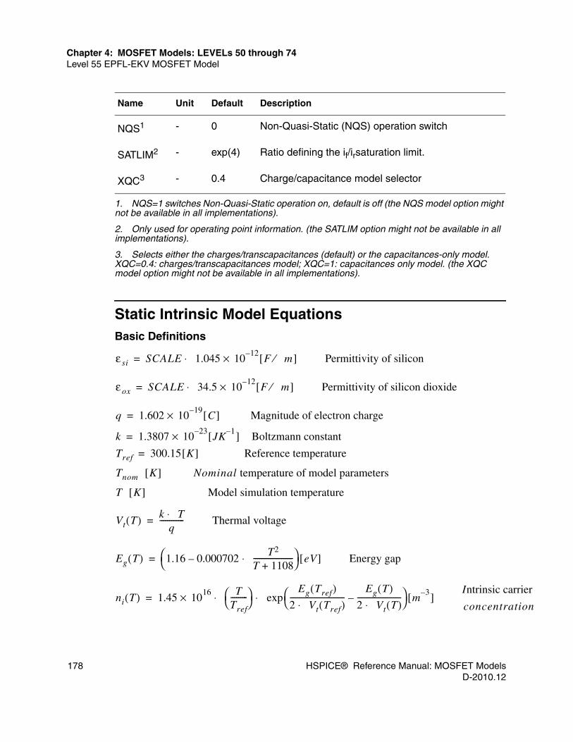
178 HSPICE® Reference Manual: MOSFET ModelsD-2010.12
Chapter 4: MOSFET Models: LEVELs 50 through 74Level 55 EPFL-EKV MOSFET Model
Static Intrinsic Model EquationsBasic Definitions
Name Unit Default Description
NQS1 - 0 Non-Quasi-Static (NQS) operation switch
SATLIM2 - exp(4) Ratio defining the if/irsaturation limit.
XQC3 - 0.4 Charge/capacitance model selector
1. NQS=1 switches Non-Quasi-Static operation on, default is off (the NQS model option might not be available in all implementations).
2. Only used for operating point information. (the SATLIM option might not be available in all implementations).
3. Selects either the charges/transcapacitances (default) or the capacitances-only model. XQC=0.4: charges/transcapacitances model; XQC=1: capacitances only model. (the XQC model option might not be available in all implementations).
ε si SCALE 1.045 1012–×⋅ F m⁄[ ]= Permittivity of silicon
ε ox SCALE 34.5 1012–×⋅ F m⁄[ ]= Permittivity of silicon dioxide
q 1.602 1019–× C[ ]= Magnitude of electron charge
k 1.3807 1023–× JK
1–[ ]= Boltzmann constant
Tref 300.15 K[ ]= Reference temperature
Tnom K[ ] Nominal temperature of model parameters
T K[ ] Model simulation temperature
Vt T( ) k T⋅q
-------------= Thermal voltage
Eg T( ) 1.16 0.000702T2
T 1108+---------------------⋅–⎝ ⎠
⎛ ⎞ eV[ ]= Energy gap
ni T( ) 1.45 1016× T
Tref---------⎝ ⎠
⎛ ⎞ Eg Tref( )2 Vt Tref( )⋅-----------------------------
Eg T( )2 Vt T( )⋅-----------------------–⎝ ⎠
⎛ ⎞ m3–[ ]exp⋅ ⋅=
Intrinsic carrier
concentration

HSPICE® Reference Manual: MOSFET Models 179D-2010.12
Chapter 4: MOSFET Models: LEVELs 50 through 74Level 55 EPFL-EKV MOSFET Model
Parameter PreprocessingHandling of Model Parameters for P-Channel MOSFETsFor P-channel devices, simulation reverses the sign of VFB, VTO, and TCV before processing. Therefore, VTO and TCV are usually positive and VFB is usually negative for N-channel, and vice versa for P-channel MOSFETs.
Initializing Intrinsic Parameters The basic intrinsic model parameters are related to the fundamental process parameters as in early SPICE models:
COX→TOXGAMMA and PHI→NSUBVTO→VFBKP→UOUCRIT→VMAX
For statistical circuit simulation, you should introduce parameter variations on the level of the latter parameters. You can also use these dependencies to analyze device scaling and to obtain parameter sets from other MOSFET models. Therefore, you can use the following relations:
If you do not specify COX, simulation initializes it as:
If you do not specify GAMMA, simulation initializes it as:
If you do not specify PHI, simulation initializes it as:
If you do not specify VTO, simulation initializes it as:
COXε ox TOX⁄ for: TOX > 0
default otherwise⎩⎨⎧
=
GAMMA2qε si NSUB 10
6⋅( )⋅COX
------------------------------------------------------------- for: NSUB > 0
default otherwise⎩⎪⎨⎪⎧
=
PHI2Vt Tnom( ) NSUB 10
6⋅ni Tnom( )
-------------------------------⎝ ⎠⎜ ⎟⎛ ⎞
ln⋅ for: NSUB > 0
default otherwise⎩⎪⎨⎪⎧
=

180 HSPICE® Reference Manual: MOSFET ModelsD-2010.12
Chapter 4: MOSFET Models: LEVELs 50 through 74Level 55 EPFL-EKV MOSFET Model
If you do not specify DP, simulation initializes it as:
If you do not specify UCRIT, simulation initializes it as:
If you do not specify E0, simulation uses a simplified mobility model with the THETA parameter:
Note: The E0 value is zero, indicating to use the simplified mobility model is used in conjunction with THETA, instead of the standard mobility model.
Optional parameters might not be available in all implementations.
Default Values and Parameter RangesIf you do not define a specific model parameters, simulation either initializes it according to the above relations, or sets it to its default value. Certain parameters restrict their numerical range to avoid numerical problems, such as divisions by zero. If you specify a parameter value outside the specified range (see the range column in the parameter tables), then simulation sets its value to the closest acceptable value.
Intrinsic Parameters Temperature Dependence
VTOVFB PHI GAMMA PHI⋅+ + if you specify VFB
default otherwise⎩⎨⎧
=
KP UO 104–⋅( ) COX⋅ for: UO > 0
default otherwise⎩⎨⎧
=
UCRIT VMAX UO 104–⋅( )⁄ for: VMAX > 0 UO > 0,
default otherwise⎩⎨⎧
=
E0 0 if you specify THETA
default otherwise⎩⎨⎧
=
VTO T( ) VTO TCV T Tnom–( )⋅–=
KP T( ) KPT
Tnom-----------⎝ ⎠
⎛ ⎞ BEX⋅=

HSPICE® Reference Manual: MOSFET Models 181D-2010.12
Chapter 4: MOSFET Models: LEVELs 50 through 74Level 55 EPFL-EKV MOSFET Model
Bulk Referenced Intrinsic VoltagesSimulation refers all voltages to the local substrate (see Bulk Reference and Symmetry on page 173):
For P-channel devices, simulation inverts all signs before processing.
Effective Channel Length and Width
Note: Unlike the convention in other MOSFET models, DL and DW usually permit a negative value due to the above definition.
Short Distance MatchingThe inverse of the square root of the transistor area usually suitably describes a random mismatch between two transistors with an identical layout and close to each other. The following relationships have been adopted:
UCRIT T( ) UCRITT
Tnom-----------⎝ ⎠
⎛ ⎞ UCEX⋅=
PHI T( ) PHIT
Tnom-----------⋅ 3 Vt
TTnom-----------⎝ ⎠
⎛ ⎞ln⋅ ⋅ Eg Tnom( ) TTnom-----------⋅ Eg T( )+––=
IBB T( ) IBB 1.0 IBBT T Tnom–( )⋅+[ ]⋅=
VG VGB VGS VBS–= = Intrinsic gate-to-bulk voltage
VS VSB V– BS= = Intrinsic source-to-bulk voltage
VD VDB VDS VBS–= = Intrinsic drain-to-bulk voltage
Weff W DW+=
Leff L DL+=
VTOa VTOAVTO
NP W⋅ eff NS Leff⋅ ⋅------------------------------------------------------------+=
KPa KP 1AKP
NP W⋅ eff NS Leff⋅ ⋅------------------------------------------------------------+⎝ ⎠
⎛ ⎞⋅=

182 HSPICE® Reference Manual: MOSFET ModelsD-2010.12
Chapter 4: MOSFET Models: LEVELs 50 through 74Level 55 EPFL-EKV MOSFET Model
These model equations apply only in Monte-Carlo and sensitivity simulations. Because negative values for both KPa and GAMMAa are not physically meaningful, simulation clips them at zero.
Reverse Short-channel Effect (RSCE)
Effective Gate Voltage Including RSCE
Effective substrate factor including charge-sharing for short and narrow channelsPinch-off voltage for narrow-channel effect:
Effective substrate factor accounting for charge-sharing:
Note: This equation prevents a negative value in the square roots argument in the subsequent code.
GAMMAa GAMMAAGAMMA
NP W⋅ eff NS Leff⋅ ⋅------------------------------------------------------------+=
Cε 4 223–× 10( )
2⋅= CA 0.028=
ξ CA 10Leff
LK--------⋅ 1–⎝ ⎠
⎛ ⎞⋅=
ΔVRSCE2 Q0⋅COX
----------------- 1
112--- ξ ξ 2
Cε++( )⋅+2
-------------------------------------------------------------------⋅=
V ′G VG VTOa ΔVRSCE– PHI GAMMAa+ + PHI–=
VP0V ′G P– HI GAMMAa V ′G
GAMMAa
2-------------------------⎝ ⎠
⎛ ⎞2
+GAMMAa
2-------------------------–
⎝ ⎠⎜ ⎟⎛ ⎞
– for: V ′G 0>
PHI– for: V ′G 0≤⎩⎪⎨⎪⎧
=
V′ S D( )12--- VS D( ) PHI VS D( ) PHI+( )2
4Vt( )2++ +[ ]⋅=

HSPICE® Reference Manual: MOSFET Models 183D-2010.12
Chapter 4: MOSFET Models: LEVELs 50 through 74Level 55 EPFL-EKV MOSFET Model
Note: This equation prevents the effective substrate factor from becoming negative.
Pinch-off Voltage Including Short-Channel and Narrow-Channel Effects
Note: The pinch-off voltage accounts for channel doping effects, such as the threshold voltage and the substrate effect.
For long-channel devices, Vp is a function of gate voltage; for short-channel devices, it also becomes a function of the source and drain voltage due to the charge-sharing effect.
Slope Factor
Note: The slope factor (or body effect factor) is primarily a function of the gate voltage, and links to the weak inversion slope.
Large Signal Interpolation FunctionF(v) is the large-signal interpolation function, relating normalized currents to normalized voltages. A simple and accurate expression for the transconductance-to-current ratio consistently formulates:
γ ° GAMMAa
ε si
COX------------ LETA
Leff--------------- V′ S V′D+( )⋅ 3 WETA⋅
Weff--------------------------- VP0 PHI+⋅–⋅–=
γ ′ 12--- γ ° γ ° 2
0.1 Vt⋅++( )⋅=
VP
V ′G P– HI γ ′ V ′Gγ ′2
-------⎝ ⎠⎛ ⎞ 2
+γ ′2
-------–⎝ ⎠⎛ ⎞⋅– for: V ′G 0>
PHI– for: V ′G 0≤⎩⎪⎨⎪⎧
=
n 1GAMMAa
2 VP PHI 4Vt+ +⋅-----------------------------------------------------+=

184 HSPICE® Reference Manual: MOSFET ModelsD-2010.12
Chapter 4: MOSFET Models: LEVELs 50 through 74Level 55 EPFL-EKV MOSFET Model
■ The static large-signal interpolation function.■ The dynamic model for the intrinsic charges (and capacitances).■ The intrinsic time constant and the thermal noise model for the whole range
of current, from weak to strong inversion.
Large-signal interpolation function:
You cannot analytically invert this equation. However, you can use a Newton-Raphson iterative scheme to invert this equation. Currently, this model uses a simplified algorithm that avoids iteration, leading to a continuous expression for the large signal interpolation function.
The (inverted) large signal interpolation function has the following asymptotes in strong and weak inversion:
Forward Normalized Current
Velocity Saturation Voltage
Note: This equation accounts for the NS multiple series device number:
gms Vt⋅IDS
-------------------- 1
0.25 i+ 0.5+------------------------------------=
y 0.25 i+ 0.5–=
v 2y y( )ln+=
F v( ) v 2⁄( )2for: v >> 0
v( )exp for: v << 0⎩⎨⎧
=
if FVP VS–
Vt------------------=
VC UCRIT NS L⋅ eff⋅=
VDSS VC14---
Vt
VC------ if⋅+
12---–⋅=

HSPICE® Reference Manual: MOSFET Models 185D-2010.12
Chapter 4: MOSFET Models: LEVELs 50 through 74Level 55 EPFL-EKV MOSFET Model
Note: The VDSS variable is half the value of the actual saturation voltage.
Drain-to-source Saturation Voltage for Reverse Normalized Current
Channel-length Modulation
Equivalent Channel Length Including Channel-length Modulation and Velocity Saturation
Note: These equations also account for the NS multiple series device number.
VDSS′ VC14---
Vt
VC------ if
34--- if( )ln⋅–⎝ ⎠
⎛ ⎞⋅+12---–⋅ Vt
VC
2Vt--------⎝ ⎠
⎛ ⎞ln 0.6–⋅+=
ΔV 4 Vt LAMBDA if
VDSS
Vt------------–⎝ ⎠
⎛ ⎞⋅ 164------+⋅ ⋅=
Vds
VD VS–
2-------------------=
Vip VDSS2 ΔV
2+ Vds VDSS–( )2 ΔV
2+–=
LC
ε si
COX------------ XJ⋅=
ΔL LAMBDA LC 1Vds Vip–
LC UCRIT⋅--------------------------------+⎝ ⎠
⎛ ⎞ln⋅ ⋅=
L′ NS L⋅ eff ΔL–Vds Vip+
UCRIT----------------------+=
Lmin NS L⋅ eff 10⁄=
Leq12--- L′ L′ 2
Lmin2
++( )⋅=

186 HSPICE® Reference Manual: MOSFET ModelsD-2010.12
Chapter 4: MOSFET Models: LEVELs 50 through 74Level 55 EPFL-EKV MOSFET Model
Note: This equation prevents the equivalent channel length from becoming zero or negative.
Reverse Normalized CurrentReverse normalized current:
Reverse normalized current for the mobility model, intrinsic charges/capacitances, the thermal noise model, and the NQS time-constant:
Transconductance Factor and Mobility Reduction Due to Vertical Field
Note: The NP (or M) device parameter returns accurate results for simulating parallel devices. Using NS (or N) for series devices is only approximate.
Leq accounts for multiple NS series device numbers.
ir′ FVP Vds VS– VDSS′ 2 ΔV
2+ Vds VDSS′–( )2 ΔV
2++––
Vt----------------------------------------------------------------------------------------------------------------------------------------------=
ir FVP VD–
Vt-------------------=
β0 KPa
NP W⋅ eff
Leq-------------------------⋅=
η1 2⁄ for NMOS
1 3⁄ for PMOS⎩⎨⎧
=
qB0 GAMMAa PHI⋅=
β0′ β0 1COX
E0 ε si⋅-------------------- qB0⋅+⎝ ⎠
⎛ ⎞⋅=
ββ0′
1COX
E0 ε si⋅-------------------- Vt qB η qI⋅+⋅ ⋅+
-------------------------------------------------------------------------------=

HSPICE® Reference Manual: MOSFET Models 187D-2010.12
Chapter 4: MOSFET Models: LEVELs 50 through 74Level 55 EPFL-EKV MOSFET Model
For the definition of the qB normalized depletion and the qI inversion charges refer to the Normalized Intrinsic Node Charges on page 189. Use β0’ to ensure that
when
. The formulation of β arises from the integration of the local effective field as a function of depletion and inversion charge densities along the channel. You do not need to specify the substrate bias dependency, because the model includes the depletion charge.
Note: The resulting mobility expression also depends on VDS.
Simple Mobility Reduction ModelFor compatibility with the former EKV model versions (before v2.6), you can choose the simpler mobility reduction model, which uses the THETA parameter.
If you do not specify the E0 model parameter (see Parameter Preprocessing on page 179), simulation uses the simpler mobility model:
Specific Current
Drain-to-source Current
For P-channel devices, IDS has a negative sign.
This drain current expression is a single equation, valid in all operating regions:
β β0≈
qI <<qB
V ′P12--- VP VP
22Vt
2++( )⋅=
ββ0
1 THETA VP′⋅+----------------------------------------------=
IS 2 n β Vt2⋅ ⋅ ⋅=
IDS IS if i′ r–( )⋅=

188 HSPICE® Reference Manual: MOSFET ModelsD-2010.12
Chapter 4: MOSFET Models: LEVELs 50 through 74Level 55 EPFL-EKV MOSFET Model
■ weak, moderate and strong inversion■ non-saturation■ saturation
This current is therefore not only continuous among all of these regions, but also continuously derivable.
TransconductancesSimulation derives the transconductances from the drain current:
In the following relationships, the source for the derivatives is a reference:
This model includes the analytic derivatives.
Impact Ionization Current
Note: The factor 2 in the vib expression accounts for the fact that the numerical value of VDSS is half of the actual saturation voltage. The substrate current is a component of the total extrinsic drain current, flowing from the drain to the bulk. This model therefore expresses the total drain current as
Note: The substrate current therefore also affects the total extrinsic conductances, especially the drain conductance.
gmg VG∂∂IDS≡ gms
VS∂∂IDS–≡ gmd VDS∂
∂IDS≡
gm VGS∂∂IDS≡ gmg= gmbs VBS∂
∂IDS≡ gms gmg gmd––= gds VDS∂∂IDS≡ gmd=
Vib VD VS IBN 2 VDSS⋅ ⋅––=
IDB
IDSIBAIBB---------- Vib⋅
IBB LC⋅–
Vib---------------------------⎝ ⎠
⎛ ⎞exp⋅ ⋅ for:Vib 0>
0 for:Vib 0≤⎩⎪⎨⎪⎧
=
ID IDS IDB+=

HSPICE® Reference Manual: MOSFET Models 189D-2010.12
Chapter 4: MOSFET Models: LEVELs 50 through 74Level 55 EPFL-EKV MOSFET Model
Quasi-static Model EquationsMOSFET Level 55 includes both a charge-based model for transcapacitances, allowing charge-conservation during transient analysis, you can select a simpler capacitances-based model instead.
Note: The charges model is symmetrical in terms of the forward and reverse normalized currents—that is, the model is symmetrical for both the drain and source sides.
The pinch-off voltage in the dynamic model provides the short-channel effects (such as charge-sharing and reverse short-channel effects).
Dynamic Model for the Intrinsic Node Charges
Normalized Intrinsic Node Charges
nq 1GAMMAa
2 VP PHI 106–
+ +⋅-------------------------------------------------------+=
xf14--- if+=
xr14--- ir+=
qD nq415------
3xr3
6xr2xf 4xrxf
22xf
3+ + +
xf xr+( )2--------------------------------------------------------------⋅ 1
2---–
⎝ ⎠⎜ ⎟⎛ ⎞
⋅–=
qS nq415------
3xf3
6xf2xr 4xfxr
22xr
3+ + +
xf xr+( )2--------------------------------------------------------------⋅ 1
2---–
⎝ ⎠⎜ ⎟⎛ ⎞
⋅–=
qI qS qD+ nq43---
xf2
xfxr xr2
+ +
xf xr+--------------------------------⋅ 1–
⎝ ⎠⎜ ⎟⎛ ⎞
⋅–= =

190 HSPICE® Reference Manual: MOSFET ModelsD-2010.12
Chapter 4: MOSFET Models: LEVELs 50 through 74Level 55 EPFL-EKV MOSFET Model
qox is a fixed oxide charge, which simulation assumes is zero. The preceding equations express the charge conservation among the four nodes of the transistor.
Total Charges
Intrinsic CapacitancesTranscapacitancesSimulation derives the intrinsic capacitances from the node charges for the terminal voltages:
The preceding equation uses the positive sign if x=y or the negative sign otherwise. This equation produces simple, continuous analytical expressions for all transcapacitances in terms of the xf pinch-off voltage, the xr slope factor, and derivatives thereof, from weak to strong inversion, and from non-saturation to saturation.
Normalized Intrinsic CapacitancesSet XQC=1 to select a simplified capacitive dynamic model that uses the five intrinsic capacitances corresponding to the Level 55 Equivalent Circuit on page 174. This model ignores the slight bias dependence of the n slope factor. The result is the following simple set of functions:
qB
GAMMAa VP PHI 106–
+ +⋅–( ) 1Vt-----⋅
nq 1–
nq--------------⎝ ⎠
⎛ ⎞ qI⋅– for:V ′ G 0>
V– ′ G1Vt-----⋅ for:V ′ G 0≤
⎩⎪⎪⎨⎪⎪⎧
=
qG qI qOX qB–––=
Cox COX NP W⋅ eff NS Leff⋅ ⋅⋅=
Q I B D S G, , , ,( ) Cox Vt q I B D S G, , , ,( )⋅ ⋅=
Cxy Vy∂∂
Qx( )±= x y, G D S B, , ,=
cgs23--- 1
xr2
xr12---xf+ +
xf xr+( )2------------------------------–
⎝ ⎠⎜ ⎟⎜ ⎟⎛ ⎞
⋅=

HSPICE® Reference Manual: MOSFET Models 191D-2010.12
Chapter 4: MOSFET Models: LEVELs 50 through 74Level 55 EPFL-EKV MOSFET Model
Total Intrinsic Capacitances
Intrinsic Noise Model EquationsThe INDS current source models the noise between the intrinsic source and the drain. This noise includes a thermal noise component and a flicker noise component, and has the following Power Spectral Density (PSD):
Thermal NoiseThe following equation calculates the PSD thermal noise component:
The preceding thermal noise expression is valid in all regions of operation, including for small VDS.
Flicker NoiseThe following equation calculates the PSD flicker noise component:
In some implementations, you can select different expressions.
cgd23--- 1
xf2
xf12---xr+ +
xf xr+( )2------------------------------–
⎝ ⎠⎜ ⎟⎜ ⎟⎛ ⎞
⋅=
cgb
nq 1–
nq--------------⎝ ⎠
⎛ ⎞ 1 cgs– cgd–( )⋅=
csb nq 1–( ) cgs⋅=
cdb nq 1–( ) cgd⋅=
C gs gd gb sb db, , , ,( ) Cox c gs gd gb sb db, , , ,( )⋅=
SINDS Sthermal Sflicker+=
Sthermal 4kTμeff
NS L⋅ eff( )2------------------------------ QI⋅ ⋅ 4kT β qI⋅ ⋅= =
Sflicker
KF gmg2⋅
NP W⋅ eff NS L⋅ eff COX fAF⋅⋅ ⋅-------------------------------------------------------------------------------------------=

192 HSPICE® Reference Manual: MOSFET ModelsD-2010.12
Chapter 4: MOSFET Models: LEVELs 50 through 74Level 55 EPFL-EKV MOSFET Model
Operating Point InformationAt operating points, the following information displays to help in circuit design.
Numerical values of model internal variablesThe following are the intrinsic charges and capacitances:
VG, VS, VD, IDS, IDB, gmg, gms, gmbs, gmd, VP, n, β, IS, if, ir’, t, t0.
Transconductance efficiency factor
Early voltage
Overdrive voltage
For P-channel devices, has a negative sign.
SPICE-like threshold voltage
This expression is the SPICE-like threshold voltage (the source). It also accounts for charge-sharing and reverse short-channel effects on the threshold voltage.
For P-channel devices, VTH has a negative sign.
Saturation voltage
For P-channel devices, VDSAT has a negative sign.
tef gms Vt IDS⁄⋅=
VM IDS gmd⁄=
n VP VS–( )⋅ VG VTOa n VS⋅––≈
n VP VS–( )⋅
VTH VTOa ΔVRSCE γ ′ V′ S GAMMAa PHI⋅–⋅+ +=
VDSAT 2VDSS 4Vt+=

HSPICE® Reference Manual: MOSFET Models 193D-2010.12
Chapter 4: MOSFET Models: LEVELs 50 through 74Level 55 EPFL-EKV MOSFET Model
Saturation / non-saturation flag:
Note: Some simulators implement the operating point differently (some information might not be available).
Estimation and Limits of Static Intrinsic Model ParametersIf you do not have access to a parameter extraction facility, simulation can roughly estimate the EKV intrinsic model parameters from the SPICE Level 2/3 parameters as indicated in Table 30. Pay attention to the units of the parameters. This estimation method generally returns reasonable results. Nevertheless, be aware that the underlying modeling in SPICE Level 2/3 and in the EKV model is not the same, even if the names and the function of several parameters are similar. Therefore, it is preferred if parameter extraction is made directly from measurements.
Lower and upper limits indicated in the table should give an idea on the order of magnitude of the parameters but do not necessarily correspond to physically meaningful limits, nor to the range specified in the parameter tables. These limits may be helpful for obtaining physically meaningful parameter sets when using nonlinear optimization techniques to extract EKV model parameters.
Table 30 Static Intrinsic Model Limits
Name Unit Default Example Lower Upper Estimation1
COX F/m2 0.7E-3 3.45E-3 - -
XJ m 0.1E-6 0.15E-6 0.01E-6 1E-6 XJ
VTO V 0.5 0.7 0 2 VTO
GAMMA 1.0 0.7 0 2
PHI2 V 0.7 0.5 0.3 2
′ SAT′ or ′ 1′ forif
ir--- SATLIM>
′ LIN′ or ′ 0′ forif
ir--- SATLIM≤
εox/TOX
V 2qεsi NSUB⋅ COX⁄
2Vt NSUB ni⁄( )ln⋅

194 HSPICE® Reference Manual: MOSFET ModelsD-2010.12
Chapter 4: MOSFET Models: LEVELs 50 through 74Level 55 EPFL-EKV MOSFET Model
εox=0.0345E-9 F/m q=1.609E-19 C k=1.381E-23 J/K
εsi=0.104E-9 F/m ni=1.45E16 m-3 Vt=kT/q=0.0259 V (at room
temperature)
KP A/V2 50E-6 150E-6 10E-6 -
E0 V/m 1.0E12 200E6 -
UCRIT V/m 2.0E6 2.3E6 1.0E6 25E6 VMAX/UO
DL m 0 -0.15*Lmin -0.5*Lmin 0.5*Lmin
DW m 0 -0.1*Wmin -0.5*Wmin 0.5*Wmi
LAMBDA - 0.5 0.8 0 3 -
LETA - 0.1 0.3 0 2 -
WETA - 0.25 0.2 0 2 -
Q0 As/ 0.0 230E-6 0 - -
LK m 0.29E-6 0.4E-6 0.05E-6 2E-6 -
IBA 1/m 0.0 2.0E8 0.0 5.0E8
IBB V/m 3.0E8 2.0E8 1.8E8 4.0E8
IBN - 1.0 0.6 0.4 1.0 -
1. Also compare with optional process parameters.
2. The minimum value of PHI also determines the minimum value of the pinch-off voltage. Due to the intrinsic temperature dependence of PHI, higher temperatures use a lower value, which limits the range of simulation for small currents.
Table 30 Static Intrinsic Model Limits
Name Unit Default Example Lower Upper Estimation1
UO COX⋅
0.1 0.4 TOX⋅( )⁄ 0.2 THETA TOX⋅( )⁄
XL 2 LD⋅–
XW 2 WD⋅–
ALPHA VCR LC⁄⋅
VCR LC⁄
Lc ε si XJ COX⁄⋅=

HSPICE® Reference Manual: MOSFET Models 195D-2010.12
Chapter 4: MOSFET Models: LEVELs 50 through 74Level 55 EPFL-EKV MOSFET Model
Note: Parameters in this table use m (meter) as the length unit. Lmin is the minimum drawn length of transistors. Wmin is the minimum drawn width of transistors. Example values are shown for enhancement N-channel devices.
Model Updates DescriptionSynopsys has made several improvements to the original EKV v2.6 MOSFET model. Wherever possible, these enhancements maintain backward compatibility with previous versions.
Revision I, September 1997Description:
The narrow channel effect on the substrate factor was revised to improve the transcapacitances behavior. The narrow channel effect is no longer a function of the vs source voltage, but of the vp pinch-off voltage.
Consequence:
The WETA and DW narrow channel effect parameters require different numerical values to achieve the same effect.
Revision II, July 1998Intrinsic time constantDescription:
Simulation calculates the τ 0 intrinsic time constant as a function of the effective β factor (including vertical field dependent mobility and short-channel effects), instead of the maximum mobility using the KP parameter.
Consequence:
The NQS time constant has an additional gate voltage dependence, resulting in more conservative (lower) estimation of the NQS time constant at high VG, and additional dependence on short-channel effects.

196 HSPICE® Reference Manual: MOSFET ModelsD-2010.12
Chapter 4: MOSFET Models: LEVELs 50 through 74Level 55 EPFL-EKV MOSFET Model
Thermal noiseDescription:
Simulation calculates the Sthermal thermal noise power spectral density as a function of the effective β factor (including vertical field dependent mobility and short-channel effects), instead of the maximum mobility using the KP parameter.
Consequence:
Sthermal has an additional gate voltage and short-channel effect dependence.
Optional process parameters to calculate electrical intrinsic parametersDescription:
This option calculates the electrical parameters as a function of the optional parameters:
COX→TOXGAMMA and PHI→NSUBVTO→VFBKP→UOUCRIT→VMAX
cm is the length unit for the NSUB and UO parameters.
Consequence:
These parameters accommodate scaling behavior and allow meaningful statistical circuit simulation, due to decorrelation of physical effects. If you use these optional parameters, this version is compatible with former revisions, except for the default calculation of the parameters.
Optional simplified mobility modelDescription:
The simple mobility model used in former model versions by using the THETA parameter, was reinstated as an option.
Consequence:
This mobility model simplifies adaptation from earlier model versions to the current version.
Parameter synonymsDescription:
You can use E0 and Q0 as synonyms for the EO and QO parameters.

HSPICE® Reference Manual: MOSFET Models 197D-2010.12
Chapter 4: MOSFET Models: LEVELs 50 through 74Level 55 EPFL-EKV MOSFET Model
Consequence:
This option accommodates some simulators that use only alphabetic characters.
Operating point informationDescription:
This enhancement models the analytical expression for the SPICE-like VTH threshold voltage in the operating point information to include the charge-sharing and reverse short-channel effects. This option modifies the analytical expression for the VDSAT saturation voltage in the operating point information so it has a non-zero value in weak inversion.
Consequence:
This enhancement improves design information.
Corrections from EPFL R11, March, 1999Equation 45, Equation 53, Equation 54, and Equation 58 were corrected for multiple series device behavior by using the NS parameter.
Corrections from EPFL R12, July 30, 1999EPFL released the following corrections.
Correction 1- 99/07/30 mb (r12) corrected dGAMMAprime_dVG (narrow channel). An error in the analytical model derivatives of the GAMMAprime variable affected the transconductances and transcapacitances.
Correction 2- 99/07/30 mb (r12) prevents PHI from being smaller than 0.2, both at init and after updating the temperature. For some CMOS technologies, PHI parameter values are as low as 400mV, required to account for particular process details. If you increase the temperature from room temperature, PHI decreases due to its built-in temperature dependence. As a result, PHI attains very low values or even becomes negative when it reaches 100degC. For the model to function at these temperatures, PHI has a lower limit of 200mV. The usual range for this parameter is well above this value (600mV to 1V).
Correction 3- 99/06/28 mb (r12) fixed COX/KP initialization (rg).
Correction 4- 99/05/04 mb (r12) completed parameter initialization for XQC, DL, and DW, and removed IBC and ibc (cd).
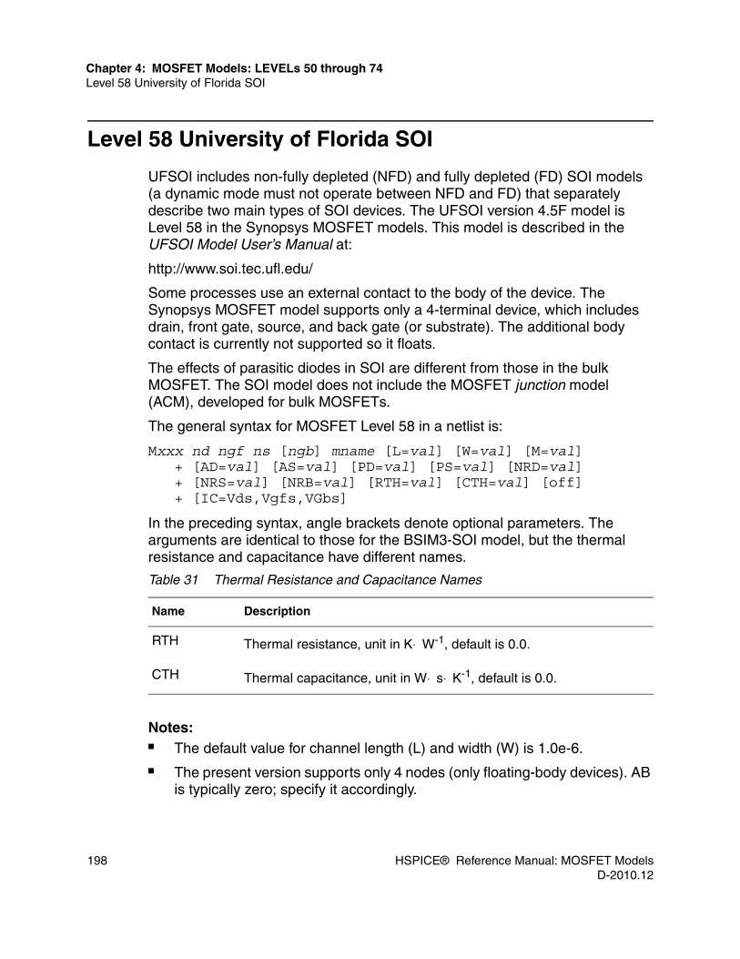
198 HSPICE® Reference Manual: MOSFET ModelsD-2010.12
Chapter 4: MOSFET Models: LEVELs 50 through 74Level 58 University of Florida SOI
Level 58 University of Florida SOI
UFSOI includes non-fully depleted (NFD) and fully depleted (FD) SOI models (a dynamic mode must not operate between NFD and FD) that separately describe two main types of SOI devices. The UFSOI version 4.5F model is Level 58 in the Synopsys MOSFET models. This model is described in the UFSOI Model User’s Manual at:
http://www.soi.tec.ufl.edu/
Some processes use an external contact to the body of the device. The Synopsys MOSFET model supports only a 4-terminal device, which includes drain, front gate, source, and back gate (or substrate). The additional body contact is currently not supported so it floats.
The effects of parasitic diodes in SOI are different from those in the bulk MOSFET. The SOI model does not include the MOSFET junction model (ACM), developed for bulk MOSFETs.
The general syntax for MOSFET Level 58 in a netlist is:
Mxxx nd ngf ns [ngb] mname [L=val] [W=val] [M=val]+ [AD=val] [AS=val] [PD=val] [PS=val] [NRD=val] + [NRS=val] [NRB=val] [RTH=val] [CTH=val] [off]+ [IC=Vds,Vgfs,VGbs]
In the preceding syntax, angle brackets denote optional parameters. The arguments are identical to those for the BSIM3-SOI model, but the thermal resistance and capacitance have different names.
Notes:■ The default value for channel length (L) and width (W) is 1.0e-6. ■ The present version supports only 4 nodes (only floating-body devices). AB
is typically zero; specify it accordingly.
Table 31 Thermal Resistance and Capacitance Names
Name Description
RTH Thermal resistance, unit in K⋅ W-1, default is 0.0.
CTH Thermal capacitance, unit in W⋅ s⋅ K-1, default is 0.0.
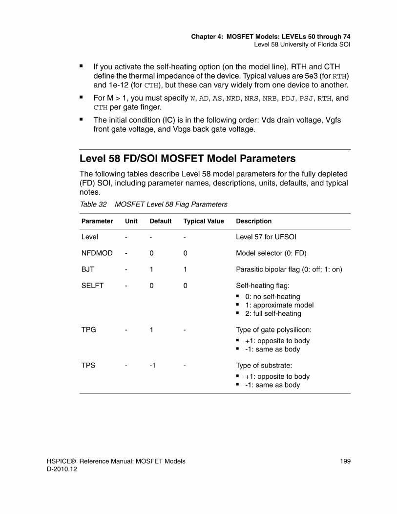
HSPICE® Reference Manual: MOSFET Models 199D-2010.12
Chapter 4: MOSFET Models: LEVELs 50 through 74Level 58 University of Florida SOI
■ If you activate the self-heating option (on the model line), RTH and CTH define the thermal impedance of the device. Typical values are 5e3 (for RTH) and 1e-12 (for CTH), but these can vary widely from one device to another.
■ For M > 1, you must specify W, AD, AS, NRD, NRS, NRB, PDJ, PSJ, RTH, and CTH per gate finger.
■ The initial condition (IC) is in the following order: Vds drain voltage, Vgfs front gate voltage, and Vbgs back gate voltage.
Level 58 FD/SOI MOSFET Model ParametersThe following tables describe Level 58 model parameters for the fully depleted (FD) SOI, including parameter names, descriptions, units, defaults, and typical notes.
Table 32 MOSFET Level 58 Flag Parameters
Parameter Unit Default Typical Value Description
Level - - - Level 57 for UFSOI
NFDMOD - 0 0 Model selector (0: FD)
BJT - 1 1 Parasitic bipolar flag (0: off; 1: on)
SELFT - 0 0 Self-heating flag:■ 0: no self-heating■ 1: approximate model■ 2: full self-heating
TPG - 1 - Type of gate polysilicon:■ +1: opposite to body■ -1: same as body
TPS - -1 - Type of substrate:■ +1: opposite to body■ -1: same as body

200 HSPICE® Reference Manual: MOSFET ModelsD-2010.12
Chapter 4: MOSFET Models: LEVELs 50 through 74Level 58 University of Florida SOI
Table 33 MOSFET Level 58 Structural Parameters
Parameter Unit Default Typical Value Description
TOXF m 1.0e-8 (3-8)x10-9 Front-gate oxide thickness
TOXB m 0.5e-6 (80-400)x10-9 Back-gate oxide thickness
NSUB cm-3 1.0e15 1015
-1017
Substrate doping density
NGATE cm-3 0.0 1019
-1020
Poly-gate doping density (0 for no poly-gate depletion)
NDS cm-3 5.0e19 1019
-1020
Source/drain doping density
TB m 0.1e-6 (30-100)x10-9
Film (body) thickness
NBODY cm-3 5.0e16 1017
-1018
Film (body) doping density
LLDD m 0.0 (0.05-0.2)x10-6 LDD/LDS region length (0 for no LDD)
NLDD cm-3 5.0e19 1x10¹⁹ LDD/LDS doping density (>1e19: LDD/LDS treated as D/S extensions)
DL m 0.0 (0.05-0.15)x10-6 Channel-length reduction
DW m 0.0 (0.1-0.5)x10-6 Channel-width reduction

HSPICE® Reference Manual: MOSFET Models 201D-2010.12
Chapter 4: MOSFET Models: LEVELs 50 through 74Level 58 University of Florida SOI
Table 34 MOSFET Level 58 Electrical Parameters
Parameter Unit Default Typical Value Description
NQFF cm-2 0.0 ~ 1010 Front oxide fixed charge (normalized)
NQFB cm-2 0.0 ~ 1011 Back oxide fixed charge (normalized)
NQFSW cm-2 0.0 ~ 1012 Effective sidewall fixed charge (0 for no narrow-width effect)
NSF cm-2⋅ eV-1 0.0 ~1010 Front surface state density
NSB cm-2⋅ eV-1 0.0 ~ 1011 Back surface state density
QM - 0.0 -0.5 Energy quantization parameter (0 for no quantization)
UO cm2⋅ V-1⋅ s-1
7.0e2 200-700 (nMOS)70-400 (pMOS)
Low-field mobility
THETA cm⋅ V-1 7.0e2 (0.1-3)x10-6 Mobility degradation coefficient
VSAT cm⋅ s-1 1.0e-6 (0.5-1)x10 Carrier saturated drift velocity
ALPHA cm-1 0.0 2.45x10⁶ Impact-ionization coefficient (0 for no impact ionization)
BETA V⋅ cm-1 0.0 1.92x10⁶ Impact-ionization exponential factor (0 for no impact ionization)
±

202 HSPICE® Reference Manual: MOSFET ModelsD-2010.12
Chapter 4: MOSFET Models: LEVELs 50 through 74Level 58 University of Florida SOI
BGIDL V⋅ cm-1 0.0 (4-8)x109 Exponential factor for gate-induced drain leakage (0 for no GIDL)
GAMMA - 0.3 0.3-1.0 BOX fringing field weighting factor
KAPPA - 0.5 0.5-1.0 BOX fringing field weighting factor
JRO A⋅ m-1 1.0e-10 10-11
-10-9
Body-source/drain junction recombination current coefficient
M - 2.0 1.0-2.0 Body-source/drain junction recombination ideality factor
LDIFF m 1.0e-7 (0.1-0.5)x10-6 Effective diffusion length in source/drain
SEFF cm⋅ s-1 1.0e5 (0.5-5)x105 Effective recombination velocity in source/drain
CGFDO F⋅ m-1 0.0 1x10⁻¹⁰ Gate-drain overlap capacitance
CGFSO F⋅ m-1 0.0 1x10⁻¹⁰ Gate-source overlap capacitance
CGFBO F⋅ m-1 0.0 0.0 Gate-body overlap capacitance
RD ohm⋅ m 0.0 200-1000 Specific drain parasitic resistance
Table 34 MOSFET Level 58 Electrical Parameters
Parameter Unit Default Typical Value Description

HSPICE® Reference Manual: MOSFET Models 203D-2010.12
Chapter 4: MOSFET Models: LEVELs 50 through 74Level 58 University of Florida SOI
RS ohm⋅ m 0.0 200-1000 Specific source parasitic resistance
RHOB ohm/sq. 0.0 30x103 Body sheet resistance
FNK F⋅ A 0.0 0-10-2 Flicker noise coefficient
FNA - 1.0 0.5-2 Flicker noise exponent
Table 35 MOSFET Level 58 Optional Parameters
Parameter Unit Default Typical Value Description
VFBF V calc. -1 (nMOS)1 (pMOS)
Front-gate flatband voltage
VFBB V calc. - Back-gate flatband voltage
WKF V calc. ~ VFBF Front-gate work function difference
WKB V calc. - Back-gate work function difference
TAUO s calc. 10-7
-10-5
Carrier lifetime in lightly doped regions
BFACT - 0.3 0.1-0.5 VDS averaging factor for mobility degradation
FVBJT - 0.0 0-1 BJT current directional partitioning factor (0 for lateral 1D flow)
RHOSD ohm/sq. 0.0 50 Source/drain sheet resistance
Table 34 MOSFET Level 58 Electrical Parameters
Parameter Unit Default Typical Value Description

204 HSPICE® Reference Manual: MOSFET ModelsD-2010.12
Chapter 4: MOSFET Models: LEVELs 50 through 74Level 58 University of Florida SOI
Level 58 NFD/SOI MOSFET Model ParametersThe following tables describe the Level 58 model parameters for non fully depleted (NFD) SOI, including parameter names, descriptions, units, defaults, and typical notes.
Table 36 MOSFET Level 58 Flag Parameters
Parameter Unit Default Typical Value Description
Level - - - Level 57 for UFSOI
NFDMOD - 0 - Model selector (1: NFD)
BJT - 1 1 Parasitic bipolar flag:■ 0: off■ 1: on
SELFT - 0 0 Self-heating flag:■ 0: no self-heating■ 1: approximate model■ 2: full self-heating
TPG - 1 1 Type of gate polysilicon■ +1: opposite to body■ -1: same as body
TPS - -1 -1 Type of substrate■ +1: opposite to body■ -1: same as body)
Table 37 MOSFET Level 58 Structural Parameters
Parameter Unit Default Typical Value Description
TOXF m 1.0e-8 (3-8)x10-9 Front-gate oxide thickness
TOXB m 0.5e-6 (80-400)x10-9 Back-gate oxide thickness
NSUB cm-3 1.0e15 1015
-1017
Substrate doping density

HSPICE® Reference Manual: MOSFET Models 205D-2010.12
Chapter 4: MOSFET Models: LEVELs 50 through 74Level 58 University of Florida SOI
NGATE cm-3 0.0 1019
-1020
Poly-gate doping density (0 for no poly-gate depletion)
NDS cm-3 5.0e19 1019
-1020
Source/drain doping density
TF m 0.2e-6 (3-8)x10-9 Silicon film thickness
TB m 0.1e-6 (30-100)x10-9 Film (body) thickness
THALO m 0.0 - Halo thickness (0 for no halo)
NBL cm-3 5.0e16 1017
-1018
Low body doping density
NBH cm-3 5.0e17 1019
-1020
Halo doping density
NHALO cm-3 - ~1018 Halo doping density
LRSCE m 0.0 ~0.1x10⁻⁶ Characteristic length for reverse short-channel effect (0 for no RSCE)
LLDD m 0.0 (0.05-0.2)x10-6 LDD/LDS region length (0 for no LDD)
NLDD cm-3 5.0e19 1x10¹⁹ LDD/LDS doping density (>1e19: LDD/LDS treated as D/S extensions)
DL m 0.0 (0.05-0.15)x10-6 Channel-length reduction
DW m 0.0 (0.1-0.5)x10-6 Channel-width reduction
Table 37 MOSFET Level 58 Structural Parameters
Parameter Unit Default Typical Value Description

206 HSPICE® Reference Manual: MOSFET ModelsD-2010.12
Chapter 4: MOSFET Models: LEVELs 50 through 74Level 58 University of Florida SOI
Table 38 MOSFET Level 58 Electrical Parameters
Parameter Unit Default Typical Value Description
NQFF cm-2 0.0 ~ 1010 Front oxide fixed charge (normalized)
NQFB cm-2 0.0 ~ 1011 Back oxide fixed charge (normalized)
NQFSW cm-2 0.0 ~ 1012 Effective sidewall fixed charge(0 for no narrow-width effect)
QM - 0.0 -0.5 Energy quantization parameter (0 for no quantization)
UO cm2⋅ V-1⋅ s-1
7.0e2 200-700 (nMOS)
70-400 (pMOS)
Low-field mobility
THETA cm⋅ V-1 7.0e2 (0.1-3)x10-6 Mobility degradation coefficient
VSAT cm⋅ s-1 1.0e-6 (0.5-1)x10 Carrier saturated drift velocity
ALPHA cm-1 0.0 2.45x10⁶ Impact-ionization coefficient (0 for no impact ionization)
BETA V⋅ cm-1 0.0 1.92x10⁶ Impact-ionization exponential factor(0 for no impact ionization)
BGIDL V⋅ cm-1 0.0 (4-8)x109 Exponential factor for gate-induceddrain leakage (0 for no GIDL)
±

HSPICE® Reference Manual: MOSFET Models 207D-2010.12
Chapter 4: MOSFET Models: LEVELs 50 through 74Level 58 University of Florida SOI
NTR cm-3 0.0 1014
-1015
Effective trap density for trap-assisted junction tunneling (0 for no tunneling)
JRO A⋅ m-1 1.0e-10 10-11
-10-9
Body-source/drain junction recombination current coefficient
M - 2.0 1.0-2.0 Body-source/drain junction recombination ideality factor
LDIFF m 1.0e-7 (0.1-0.5)x10-6 Effective diffusion length in source/drain
SEFF cm⋅ s-1 1.0e5 (0.5-5)x105 Effective recombination velocity in source/drain
CGFDO F⋅ m-1 0.0 1x10⁻¹⁰ Gate-drain overlap capacitance
CGFSO F⋅ m-1 0.0 1x10⁻¹⁰ Gate-source overlap capacitance
CGFBO F⋅ m-1 0.0 0.0 Gate-body overlap capacitance
RD ohm⋅ m 0.0 200-1000 Specific drain parasitic resistance
RS ohm⋅ m 0.0 200-1000 Specific source parasitic resistance
RHOB ohm/sq. 0.0 30x103 Body sheet resistance
Table 38 MOSFET Level 58 Electrical Parameters
Parameter Unit Default Typical Value Description

208 HSPICE® Reference Manual: MOSFET ModelsD-2010.12
Chapter 4: MOSFET Models: LEVELs 50 through 74Level 58 University of Florida SOI
FNK F⋅ A 0.0 0-10-2 Flicker noise coefficient
FNA - 1.0 0.5-2 Flicker noise exponent
Table 39 Optional MOSFET Level 58 Parameters
Parameter Unit Default Typical Value Description
VFBF V calc. -1 (nMOS)1 (pMOS)
Front-gate flatband voltage
VFBB V calc. - Back-gate flatband voltage
WKF V calc. ~ VFBF Front-gate work function difference
WKB V calc. - Back-gate work function difference
TAUO s calc. 10-7
-10-5
Carrier lifetime in lightly doped regions
BFACT - 0.3 0.1-0.5 VDS-averaging factor for mobility degradation
FVBJT - 0.0 0-1 BJT current directional partitioning factor (0 for lateral 1D flow)
RHOSD ohm/sq. 0.0 50 Source/drain sheet resistance
Table 38 MOSFET Level 58 Electrical Parameters
Parameter Unit Default Typical Value Description

HSPICE® Reference Manual: MOSFET Models 209D-2010.12
Chapter 4: MOSFET Models: LEVELs 50 through 74Level 61 RPI a-Si TFT Model
Notes:■ The model line must include LEVEL=58 and NFDMOD=0 for FD, or
NFDMOD=1 for NFD devices.■ Specifying VFBF turns off the narrow-width effect defined by NQFSW (which
can be positive or negative) and the reverse short-channel effect defined by LRSCE (and NBH or NHALO if specified); the latter effect is also turned off if you specify WKF.
■ For floating-body devices, CGFBO is small; you should set it to 0. ■ JRO and SEFF influence the gain of the BJT, but LDIFF affects only bipolar
charge storage in the source/drain. If you specify THALO, then NBH and NHALO also influence the BJT gain.
■ Loosely correlate the TAUO value with JRO in accord with basic pn-junction recombination/generation properties. Its default value is based on JRO, which is appropriate for short L; for long L, body generation predominates over that in the junctions so specify TAUO.
■ The non-local impact-ionization model is physical so do not arbitrarily vary its parameters.
■ The LDD option intensifies the model so set LLDD to 0 for large-scale circuit simulation, and add the unbiased LDD resistance to RD; this simplification stops if you specify NLDD > 1e19.
Level 58 Template OutputFor a list of output template parameters in the MOSFET models, and which parameters this model supports, see Table 4 on page 21.
Level 61 RPI a-Si TFT Model
Level 61 in the Synopsys MOSFET models is an AIM-SPICE MOS15 amorphous silicon (a-Si) thin-film transistor (TFT) model, developed by Rensselaer Polytechnic Institute.

210 HSPICE® Reference Manual: MOSFET ModelsD-2010.12
Chapter 4: MOSFET Models: LEVELs 50 through 74Level 61 RPI a-Si TFT Model
Model FeaturesFeatures of the AIM-SPICE MOS15 a-Si TFT model include:■ Modified charge control model; induced charge trapped in localized states■ Above threshold includes:
• Field effect mobility becoming a function of gate bias
• Band mobility dominated by lattice scattering■ Below threshold includes:
• Fermi level located in deep localized states
• Relate position of Fermi level, including the deep DOS, back to the gate bias
■ Empirical expression for current at large negative gate biases for hole-induced leakage current
■ Applies interpolation techniques to equations to unify the model
Using Level 61 with Synopsys SimulatorsTo simulate using the AIM-SPICE MOS15 a-Si TFT model:
1. Set Level=61 to identify the model as the AIM-SPICE MOS15 a-Si TFT model.
2. The default value for L is 100 µm, and the default value for W is 100 µm.
3. Level 61 is a 3-terminal model. This model does not include a bulk node; therefore simulation does not append parasitic drain-bulk or source-build diodes are appended to the model. You can specify a fourth node, but it does not affect simulation results.
4. The default room temperature is 25oC in Synopsys circuit simulators, but is 27oC in most other simulators. When comparing to other simulators, use .TEMP 27 or .OPTION TNOM=27 to set the simulation temperature to 27 in the netlist.
ExampleThe following is an example of how Level 61 modifies the Synopsys MOSFET model and element statement.

HSPICE® Reference Manual: MOSFET Models 211D-2010.12
Chapter 4: MOSFET Models: LEVELs 50 through 74Level 61 RPI a-Si TFT Model
mckt drain gate source nch L=10e-6 W=10e-6.MODEL nch nmos Level=61+ alphasat=0.6 cgdo=0.0 cgso=0.0 def0=0.6+ delta=5.0 el=0.35 emu=0.06 eps=11+ epsi=7.4 gamma=0.4 gmin=1e23 iol=3e-14+ kasat=0.006 kvt=-0.036 lambda=0.0008 m=2.5+ muband=0.001 rd=0.0 rs=0.0 sima0=1e-14+ tnom=27 tox=1.0e-7 v0=0.12 vaa=7.5e3+ vdsl=7 vfb=-3 vgsl=7 vmin=0.3 vto=0.0
Name Unit Default Description
ALPHASAT - 0.6 Saturation modulation parameter
CGDO F/m 0.0 Gate-drain overlap capacitance per meter channel width
CGSO F/m 0.0 Gate-source overlap capacitance per meter channel width
DEF0 eV 0.6 Dark Fermi level position
DELTA - 5 Transition width parameter
EL eV 0.35 Activation energy of the hole leakage current
EMU eV 0.06 Field effect mobility activation energy
EPS - 11 Relative dielectric constant of the substrate
EPSI - 7.4 Relative dielectric constant of the gate insulator
GAMMA - 0.4 Power law mobility parameter
GMIN m-3eV-1 1E23 Minimum density of deep states
IOL A 3E-14 Zero-bias leakage current parameter
KASAT 1/° Χ 0.006 Temperature coefficient of ALPHASAT
KVT V/° Χ -0.036 Threshold voltage temperature coefficient

212 HSPICE® Reference Manual: MOSFET ModelsD-2010.12
Chapter 4: MOSFET Models: LEVELs 50 through 74Level 61 RPI a-Si TFT Model
LAMBDA 1/V 0.0008 Output conductance parameter
M - 2.5 Knee shape parameter
MUBAND m2/Vs 0.001 Conduction band mobility
RD m 0.0 Drain resistance
RS m 0.0 Source resistance
SIGMA0 A 1E-14 Minimum leakage current parameter
TNOM οC 25 Parameter measurement temperature
TOX m 1E-7 Thin-oxide thickness
V0 V 0.12 Characteristic voltage for deep states
VAA V 7.5E3 Characteristic voltage for field effect mobility
VDSL V 7 Hole leakage current drain voltage parameter
VFB V -3 Flat band voltage
VGSL V 7 Hole leakage current gate voltage parameter
VMIN V 0.3 Convergence parameter
VTO V 0.0 Zero-bias threshold voltage
Name Unit Default Description

HSPICE® Reference Manual: MOSFET Models 213D-2010.12
Chapter 4: MOSFET Models: LEVELs 50 through 74Level 61 RPI a-Si TFT Model
Equivalent Circuit
Model Equations
Drain Current
,
,
Drain
Gate
Source
IdsCgs Cgd
Ids Ileakage Iab+= Iab gchVdse 1 LAMBDA Vds⋅+( )=
Vdse
Vds
1 Vds Vsate⁄( )+M[ ]
1 M⁄--------------------------------------------------------------=
Vsate αsatVgte=
gch
gchi
1 gchi RS RD+( )+---------------------------------------------= gchi qnsW MUBAND L⁄⋅=
ns
nsansb
nsa nsb+---------------------=
nsa
EPSI Vgte⋅q TOX⋅( )
------------------------------Vgte
Vaat----------⎝ ⎠
⎛ ⎞GAMMA
⋅=
nsb nso
tm
TOX------------
Vgfbe
V0------------EPSI
EPS-------------⎝ ⎠
⎛ ⎞
2 V0⋅Ve
-----------------
=

214 HSPICE® Reference Manual: MOSFET ModelsD-2010.12
Chapter 4: MOSFET Models: LEVELs 50 through 74Level 61 RPI a-Si TFT Model
,
,
,
Temperature Dependence
,
Capacitance
nso Nctm
Ve
V0------- DEF0
Vth---------------–⎝ ⎠
⎛ ⎞exp= Nc 3.0 1025
m3–⋅=
Ve
2 V0 Vtho⋅ ⋅2 V0 Vth–⋅
----------------------------------= tmEPS
2q GMIN⋅------------------------------=
VgteVMIN
2--------------- 1
Vgt
VMIN--------------- DELTA
2 Vgt
VMIN--------------- 1–⎝ ⎠
⎛ ⎞2
++ +=
Vgt Vgs VT–=
VgfbeVMIN
2--------------- 1
Vgfb
VMIN--------------- DELTA
2 Vgfb
VMIN--------------- 1–⎝ ⎠
⎛ ⎞2
++ +=
Vgfb Vgs VFB–= Ileakage Ihl Imin+=
Ihl IOLVds
VDSL---------------⎝ ⎠
⎛ ⎞ 1–expVgs
VGSL---------------–⎝ ⎠
⎛ ⎞ ELq
------- 1Vtho---------- 1
Vth-------–⎝ ⎠
⎛ ⎞expexp=
Imin SIGMA0 Vds⋅=
Vtho kB TNOM q⁄⋅= Vth kB TEMP( ) q⁄⋅=
Vaat VAAEMU
q GAMMA⋅--------------------------------- 1
Vth------- 1
Vtho----------–⎝ ⎠
⎛ ⎞exp=
VT VTO KVT TEMP TNOM–( )+=
αsat ALPHASAT KASAT TEMP TNOM–( )+=
Cgs Cf23---Cgc 1
Vsate Vdse–
2Vsate Vdse–-------------------------------⎝ ⎠
⎛ ⎞2
–+=
Cgd Cf23---Cgc 1
Vsate
2Vsate Vdse–-------------------------------⎝ ⎠
⎛ ⎞2
–+=

HSPICE® Reference Manual: MOSFET Models 215D-2010.12
Chapter 4: MOSFET Models: LEVELs 50 through 74Level 62 RPI Poli-Si TFT Model
Level 62 RPI Poli-Si TFT Model
Level 62 is an AIM-SPICE MOS16 poly-silicon (Poli-Si) thin-film transistor (TFT) model, developed by Rensselaer Polytechnic Institute.
The following topics are discussed in the next sections. ■ Model Features■ Using Level 62 with Synopsys Simulators■ Equivalent Circuit■ Model Equations■ Version 2 Model Equations
Model FeaturesFeatures of the AIM-SPICE MOS16 Poli-Si TFT model include:■ A design based on the crystalline MOSFET model■ Field effect mobility that becomes a function of the gate bias■ Effective mobility that accounts for trap states:
• For low Vgs, it is the power law
• For high Vgs, it is the constant
■ Reverse bias drain current function of the electric field near the drain and the temperature
■ A design independent of the channel length
Cf 0.5 EPS W Cgs qdnsc
dVgs-----------=⎝ ⎠
⎛ ⎞,⋅ ⋅=
nsc
nsacnsbc
nsac nsbc+------------------------- nsa
EPSI Vgte⋅q TOX⋅( )
------------------------------Vgte
Vaat----------⎝ ⎠
⎛ ⎞GAMMA
⋅=⎝ ⎠⎛ ⎞,=
nsbc nsb=

216 HSPICE® Reference Manual: MOSFET ModelsD-2010.12
Chapter 4: MOSFET Models: LEVELs 50 through 74Level 62 RPI Poli-Si TFT Model
■ A unified DC model that includes all four regimes for channel lengths down to 4 µm:
• Leakage (thermionic emission)
• Subthreshold (diffusion-like model)
• Above threshold (c-Si-like with mFet)
• Kink (impact ionization with feedback)■ An AC model accurately reproduces the Cgc frequency dispersion
■ Automatic scaling of model parameters that accurately model a wide range of device geometries
Using Level 62 with Synopsys SimulatorsTo simulate using the AIM-SPICE MOS16 Poli-Si TFT model:
1. Set LEVEL=62 to identify the model as the AIM-SPICE MOS16 Poli-Si TFT model.
2. The default value for L is 100 µm, and the default value for W is 100 µm.
3. Level 62 is a 3-terminal model. This model does not include a bulk node; therefore, simulation does not append a parasitic drain-bulk or source-bulk diode to the model. You can specify a fourth node, but it does not affect the simulation results.
4. The default room temperature is 25oC in Synopsys circuit simulators, but is 27oC in most other simulators. When comparing to other simulators, use .TEMP 27 or .OPTION TNOM=27 to set the simulation temperature to 27oC in the netlist.
The following is an example of how Level 62 modifies a MOSFET device model and element statement:

HSPICE® Reference Manual: MOSFET Models 217D-2010.12
Chapter 4: MOSFET Models: LEVELs 50 through 74Level 62 RPI Poli-Si TFT Model
mckt drain gate source nch L=10e-6 W=10e-6.MODEL nch nmos Level=62+ asat=1 at=3e-8 blk=0.001 bt=0.0 cgdo=0.0+ cgso=0.0 dasat=0.0 dd=1.4e-7 delta=4.0+ dg=2.0e-7 dmu1=0.0 dvt=0.0 dvto=0.0 eb=0.68 + eta=7 etac0=7 etac00=0 i0=6.0 i00=150+ lasat=0lkink=19e-6 mc=3.0 mk=1.3 mmu=3.0+ mu0=100 mu1=0.0022 mus=1.0 rd=0.0 rdx=0.0+ rs=0.0 rsx=0.0 tnom=27 tox=1.0e=7 vfb=-0.1+ vkink=9.1 von=0.0 vto=0.0
Table 40 MOSFET Level 62 Model Parameters
Name Unit Default Description
ASAT - 1 Proportionality constant of Vsat
AT m/V 3E-8 DIBL parameter 1
BLK - 0.001 Leakage barrier lowering constant
BT m . V 1.9E-6 DIBL parameter 2
CAPMOD - 0 Model capacitance selector (zero recommended)
CGDO F/m 0 Gate-drain overlap capacitance per meter channel width
CGSO F/m 0 Gate-source overlap capacitance per meter channel width
DASAT 1/° C 0 Temperature coefficient of ASAT
DD m 1400 Å Vds field constant
DELTA - 4.0 Transition width parameter
DG m 2000 Å Vgs field constant
DMU1 χμ2/ ς σ×C 0 Temperature coefficient of MU1
DVT V 0 The difference between VON and the threshold voltage
DVTO V/° C 0 Temperature coefficient of VTO

218 HSPICE® Reference Manual: MOSFET ModelsD-2010.12
Chapter 4: MOSFET Models: LEVELs 50 through 74Level 62 RPI Poli-Si TFT Model
EB EV 0.68 Barrier height of the diode
ETA - 7 Subthreshold ideality factor
ETAC0 - ETA Capacitance subthreshold ideality factor at zero-drain bias
ETAC00 1/V 0 Capacitance subthreshold coefficient of the drain bias
I0 A/m 6.0 Leakage scaling constant
I00 A/m 150 Reverse diode saturation current
KSS - 0 Small signal parameter (zero is recommended)
LASAT M 0 Coefficient for length dependence of ASAT
LKINK M 19E-6 Kink effect constant
MC - 3.0 Capacitance knee shape parameter
MK - 1.3 Kink effect exponent
MMU - 3.0 Low field mobility exponent
MU0 cm2/Vs 100 High field mobility
MU1 cm2/Vs 0.0022 Low field mobility parameter
MUS cm2/Vs 1.0 Subthreshold mobility
RD µ 0 Drain resistance
RDX 0 Resistance in series with Cgd
RS µ 0 Source resistance
RSX 0 Resistance in series with Cgs
Table 40 MOSFET Level 62 Model Parameters
Name Unit Default Description
Ω
Ω

HSPICE® Reference Manual: MOSFET Models 219D-2010.12
Chapter 4: MOSFET Models: LEVELs 50 through 74Level 62 RPI Poli-Si TFT Model
TNOM ° C 25 Parameter measurement temperature
TOX m 1e-7 Thin-oxide thickness
V0 V 0.12 Characteristic voltage for deep states
VFB V -0.1 Flat band voltage
VKINK V 9.1 Kink effect voltage
VON V 0 On-voltage
VSI V 2.0 vgs dependence parameter
VST V 2.0 vgs dependence parameter
VTO V 0 Zero-bias threshold voltage
ZEROC - 0 Flag for capacitance calculations in capmod=1■ capmod=1: set the 0 capacitance value■ capmod=0: calculation capacitance
XL m 0 Length bias accounts for the masking and etching effects
XW m 0 Width bias accounts for the masking and etching effects
LMLT - 1 Length shrink factor
WMLT - 1 Width shrink factor
COMPATIBLE=0|1 - 0 ■ COMPATIBLE=0: HSPICE implementation of AIM-SPICE MOS 16 RPI TFT model.
■ COMPATIBLE=1: Enables compatiblity to a commonly-used TFT model by the industry.
Table 40 MOSFET Level 62 Model Parameters
Name Unit Default Description

220 HSPICE® Reference Manual: MOSFET ModelsD-2010.12
Chapter 4: MOSFET Models: LEVELs 50 through 74Level 62 RPI Poli-Si TFT Model
Table 41 Model Parameters Specific to Version 2
Name Unit Default Description
VERSION - 1 1=Version 12=Version 2
ME (MS) - 2.5 Long channel saturation transition parameter
META - 1 ETA floating-body parameter
MSS - 1.5 Vdse transition parameter
VMAX m/s 4.00E+004 Saturation velocity
THETA M/V 0 Mobility degradation parameter
ISUBMOD - 0 Channel length modulation selector:0 – uses LAMBDA1 – uses LS and VP
LAMBDA 1/V Channel length modulation parameter
LS - 3.50E-008 Channel length modulation parameter
VP V 0.2 Channel length modulation parameter
INTDSNOD - 1 if VERSION=10 if VERSION=2
Extrinsic series resistance mode selector:0 - uses internal approximation for drain and source resistances1 – uses drain and source resistances as extrinsic elements
VSIGMAT V VST, if specified 1.7, otherwise
VGS dependence parameter
VSIGMA V VSI, if specified 0.2, otherwise
VGS dependence parameter

HSPICE® Reference Manual: MOSFET Models 221D-2010.12
Chapter 4: MOSFET Models: LEVELs 50 through 74Level 62 RPI Poli-Si TFT Model
DIBLMOD - 1 DIBL model selector
VSIGMAT V VST, if specified, 1.7 otherwise
VGS dependence parameter
VSIGMA V VSI, if specified, 0.2 otherwise
VGS dependence parameter
LMU0 m 0 MU0 length dependence parameter
LMU1 m 0 MU1 length dependence parameter
LME m 0 ME length dependence parameter
Table 42 Self-Heating Parameters
Name Unit Default Description
SHMOD - 0 Self-heating flag
RTH0 moC/W 0 Thermal resistance per unit width
CTH0 Ws/moC 1.00E-005 Thermal capacitance per unit width
WTH0 m 0 Width offset for thermal resistance and capacitance scaling
Table 43 ACM Parameters for Drain and Source Resistance Calculus Specific to HSPICE
Name Unit Default Description
ACM - - Area calculation method
LD m 0 Lateral diffusion into channel from source and drain diffusion
WD m 0 Lateral diffusion into channel from bulk along width
Table 41 Model Parameters Specific to Version 2
Name Unit Default Description

222 HSPICE® Reference Manual: MOSFET ModelsD-2010.12
Chapter 4: MOSFET Models: LEVELs 50 through 74Level 62 RPI Poli-Si TFT Model
Note: Source and drain resistances are calculated similarly to other HSPICE MOSFET models, which are based on the value of ACM.
Equivalent Circuit
Model EquationsThe following sections discuss these equations:
HDIF m 0 Length of heavily doped diffusion
LDIF m 0 Length of heavily doped region adjacent to gate
RDC ohm 0 Additional drain resistance due to contact
RSC ohm 0 Additional source resistance due to contact
RSH ohm/sq 0 Drain and source diffusion sheet resistance
Table 43 ACM Parameters for Drain and Source Resistance Calculus Specific to HSPICE
Name Unit Default Description
Drain
Gate
Source
IdsCgs Cgd
RSX RDX
RS RD

HSPICE® Reference Manual: MOSFET Models 223D-2010.12
Chapter 4: MOSFET Models: LEVELs 50 through 74Level 62 RPI Poli-Si TFT Model
■ Drain Current■ Threshold Voltage■ Temperature Dependence■ Capacitance■ Geometry Effect■ Self Heating
Drain CurrentTotal Current
Subthreshold CurrentThe following is the expression for the subthreshold current:
, ,
In the preceding equations, ετ is the dielectric constant of the oxide, and kB is the Boltzmanns constant.
Above the VGT > 0 threshold, the following equation calculates the conduction current:
Ids
Ia Isub⋅Ia Isub+-------------------- 1 Ikink+( ) Ileak+⋅=
Isub MUS CoxWL-----V
2sth
VGT
Vsth---------⎝ ⎠
⎛ ⎞ 1VDS
Vsth---------–⎝ ⎠
⎛ ⎞exp–exp⋅=
Isub MUS Cox
Weff
Leff---------- Vsth
2 VGT
Vsth---------⎝ ⎠
⎛ ⎞exp 1VDS
Vsth---------–⎝ ⎠
⎛ ⎞exp–⎝ ⎠⎛ ⎞⋅ ⋅ ⋅ ⋅ ⋅=
COX
ε i
TOX---------= Vsth ETA Vth⋅= Vth
kB TEMP⋅q
-----------------------------=
VGT VGS VTeff–=
VTeff VTX
AT VDS 2
BT+⋅
Leff 1VGS VST VTX––
VSI-------------------------------------------⎝ ⎠
⎛ ⎞exp+⎝ ⎠⎛ ⎞⋅
-----------------------------------------------------------------------------------------–=

224 HSPICE® Reference Manual: MOSFET ModelsD-2010.12
Chapter 4: MOSFET Models: LEVELs 50 through 74Level 62 RPI Poli-Si TFT Model
Subthreshold Leakage CurrentSubthreshold leakage current is the result of the thermionic field emission of carriers through the grain boundary trap states as described in the following equations.
The following equations calculate values for the preceding equations:
Ia
μFET COX Weff⋅ ⋅Leff
----------------------------------------------- VGTE VDS
VDS 2
2 αsat⋅-------------------–⋅
⎝ ⎠⎜ ⎟⎛ ⎞
for VDS αsat≤ VGTE
μFET COX Weff VGTE 2 αsat⋅ ⋅ ⋅ ⋅
2 Leff⋅-------------------------------------------------------------------------------------
=
for VDS>αsatVGTE
1μFET----------- 1
MUO-------------- 1
μ12 VGTE⋅
Vsth-----------------------⎝ ⎠
⎛ ⎞MMU
⋅------------------------------------------------------+=
VGTE Vsth 1VGT
2 Vsth⋅------------------- DELTA
2 VGT
2 Vsth⋅------------------- 1–⎝ ⎠
⎛ ⎞ 2++ +⋅=
Ileak IO Weff
q BLK VDS⋅ ⋅k T⋅
--------------------------------------⎝ ⎠⎛ ⎞ 1–exp XTFE XTE+( ) Idiode+⋅ ⋅ ⋅=
XTFE
XTFE, lo XTFE, hi⋅XTFE, lo XTFE, hi+------------------------------------------=
XTE WC–( )exp=
WC
EC Et–
k T⋅------------------ 0.55eV
k T⋅-----------------= =
4 π3
---------- f427------ f
2Wc–⋅⎝ ⎠
⎛ ⎞ for f flo
XTFE, lo flo( ) 1flo----- 8
27------ flo⋅+⎝ ⎠
⎛ ⎞ f flo–( )⋅ for f flo>exp⋅
≤exp⋅ ⋅XTFE,lo=

HSPICE® Reference Manual: MOSFET Models 225D-2010.12
Chapter 4: MOSFET Models: LEVELs 50 through 74Level 62 RPI Poli-Si TFT Model
Impact Ionization EffectVGT > 0ery large drain biases include the kink effect. Level 62 models this effect as impact ionization in a narrow region near the drain, and adds the Ikink impact ionization current to the drain current. The expression is:
2Wc
3---------- 1
2Wc
3----------–⎝ ⎠
⎛ ⎞ for f fhi
13 Wc
2 f⋅--------------–⎝ ⎠
⎛ ⎞1– Wc
3/2–
f---------------- for f fhi≥exp
>exp⋅XTFE,hi=
fhi 3Wc
3/2
2Wc 3–-------------------
⎝ ⎠⎜ ⎟⎛ ⎞
⋅=
fFmin
2----------- 1
Ff
Ffo-------
Fmin----------- DELTA
2
Ff
Ffo-------
Fmin----------- 1–
⎝ ⎠⎜ ⎟⎜ ⎟⎜ ⎟⎛ ⎞
2
++ +=
Fmin 1e4–
=
XTFE,lo flo( ) 2 4π3
-------------- flo427------flo
2Wc–⎝ ⎠
⎛ ⎞exp⋅ ⋅=
Ff
VDS
DD---------
VGS VFB–
DG---------------------------–⎝ ⎠
⎛ ⎞=
Ffo k T⋅( )3 2⁄ 43--- 2π 2m*
q h⋅----------------------⋅⎝ ⎠
⎛ ⎞⋅=
m* 0.27 m0⋅=
flo32--- Wc 1+ 1–( )⋅=
Idiode IOO WeffEB
k T⋅-------------–⎝ ⎠
⎛ ⎞ 1q VDS⋅
k T⋅-------------------–⎝ ⎠
⎛ ⎞exp–exp⋅ ⋅=

226 HSPICE® Reference Manual: MOSFET ModelsD-2010.12
Chapter 4: MOSFET Models: LEVELs 50 through 74Level 62 RPI Poli-Si TFT Model
Threshold VoltageIf you do not specify VTO, then VT=VON-DVT. Otherwise, VT=VTO.
Temperature Dependence
CapacitanceCAPMOD=0
Ikink Akinkt VDS VDSE–( ) VKINKVDS VDSE–----------------------------–⎝ ⎠
⎛ ⎞exp⋅ ⋅=
Akinkt1
VKINK------------------- LKINK
Leff------------------⎝ ⎠
⎛ ⎞ MK=
VDSEVDS
1VDS
VDSAT---------------⎝ ⎠
⎛ ⎞3
+⎝ ⎠⎛ ⎞
1 3⁄------------------------------------------------ Vth–=
VDSAT αsat VGTE⋅=
VTX VT DVTO TEMP TNOM–( )⋅–=
μ1 MU1 DMU1 TEMP TNOM–( )⋅+=
αsat ASATLASAT
Leff------------------ DASAT TEMP TNOM–( )⋅––=
Cgs Cf23--- Cgcs 1
VDSAT VDSEX–
2VDSAT VDSEX–----------------------------------------⎝ ⎠
⎛ ⎞2
–⋅ ⋅+=
Cgd Cf23--- Cgcd 1
VDSAT
2VDSAT VDSEX–----------------------------------------⎝ ⎠
⎛ ⎞2
–⋅ ⋅+=
Cf 0.5 EPS Weff⋅ ⋅=
Cgcd
COX
1 ηcd
VGTX
ηcd Vth⋅---------------------–⎝ ⎠
⎛ ⎞exp⋅+
---------------------------------------------------------------=
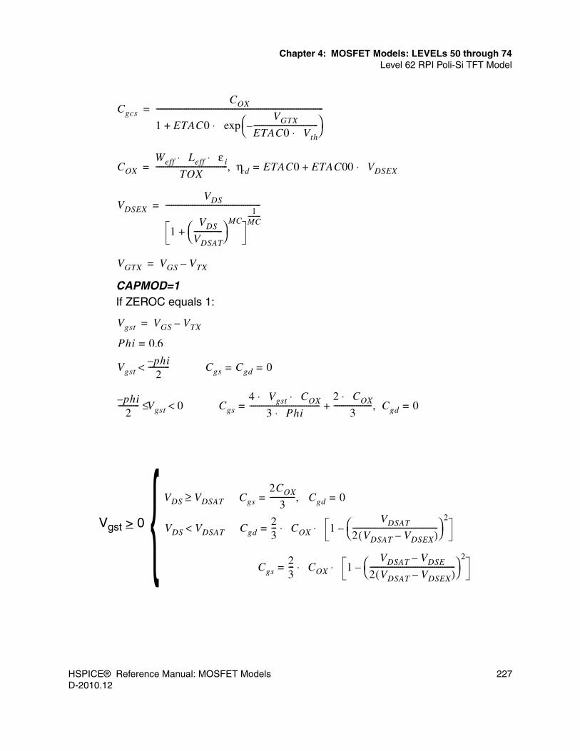
HSPICE® Reference Manual: MOSFET Models 227D-2010.12
Chapter 4: MOSFET Models: LEVELs 50 through 74Level 62 RPI Poli-Si TFT Model
CAPMOD=1If ZEROC equals 1:
Cgcs
COX
1 ETAC0VGTX
ETAC0 Vth⋅----------------------------------–⎝ ⎠
⎛ ⎞exp⋅+
----------------------------------------------------------------------------------------=
COX
Weff Leff ε i⋅ ⋅TOX
-------------------------------------- ηcd ETAC0 ETAC00 VDSEX⋅+=,=
VDSEX
VDS
1VDS
VDSAT---------------⎝ ⎠
⎛ ⎞MC
+
1MC---------
--------------------------------------------------=
VGTX VGS VTX–=
Vgst VGS VTX
Phi 0.6=
–=
Vgstphi–2
----------- Cgs Cgd 0= =<
phi–2
----------- Vgst 0 Cgs
4 Vgst COX⋅ ⋅3 Phi⋅
-------------------------------------2 COX⋅
3-------------------- Cgd,+ 0= =<≤
VDS VDSAT Cgs
2COX
3------------- Cgd 0
VDS VDSAT Cgd23--- COX 1
VDSAT
2 VDSAT VDSEX–( )---------------------------------------------⎝ ⎠
⎛ ⎞2
–
Cgs23--- COX 1
VDSAT VDSE–
2 VDSAT VDSEX–( )---------------------------------------------⎝ ⎠
⎛ ⎞2
–⋅ ⋅=
⋅ ⋅=<
=,=≥
Vgst > 0

228 HSPICE® Reference Manual: MOSFET ModelsD-2010.12
Chapter 4: MOSFET Models: LEVELs 50 through 74Level 62 RPI Poli-Si TFT Model
,
Geometry Effect
Self HeatingSelf heating is turned on if self-heating parameters SHMOD=1 and RTH0 > 0.
SHMOD and RTH0 are also instance parameters. They override the corresponding model parameters.
The effective thermal resistance and capacitance equations and equivalent circuit are:
Version 2 Model EquationsThe RPI TFT poly-Si Version 2 model is available in HSPICE. Invoke the model by setting the VERSION parameter to 2.
The following sections display these equations:
COX
ε i Weff Leff⋅ ⋅TOX
--------------------------------------= VDSEX
VDS
1VDS
VDSAT---------------⎝ ⎠
⎛ ⎞MC
+
1MC---------
--------------------------------------------------=
Weff W XW
Leff L XL+=
+=
RthRTH0
Weff WTH0eff+--------------------------------------=
Cth CTH0 Weff WTH0eff+( )⋅=
P
T
Rth Cth

HSPICE® Reference Manual: MOSFET Models 229D-2010.12
Chapter 4: MOSFET Models: LEVELs 50 through 74Level 62 RPI Poli-Si TFT Model
■ Threshold Voltage and VGS - VT
■ Mobility■ Channel Conductance■ Saturation Voltage and Effective Vds
■ Drain Current■ Total Drain Current, including Kink Effect and Leakage■ Additional Geometry Scaling for Version 2■ Temperature Dependence for Version 2
Threshold Voltage and VGS - VT
If DIBLMOD = 0, then
else, if DIBLMOD = 1, then
otherwise
VTeff VTX ΔVT DIBL,–=
ΔVT DIBL,AT VDS
2BT+⋅
Leff-----------------------------------------=
ΔVT DIBL,AT VDS
2BT+⋅
Leff 1VGS VSIGMAT VTX––
VSIGMA----------------------------------------------------------⎝ ⎠
⎛ ⎞exp+⋅--------------------------------------------------------------------------------------------------------=
ΔVT DIBL,AT VDS
2⋅
Leff 1VGS VSIGMAT VTX––
VSIGMA----------------------------------------------------------⎝ ⎠
⎛ ⎞exp+⋅-------------------------------------------------------------------------------------------------------- BT
Leff----------+=
VGT VGS VTeff–=
VGTE ETA V⋅ th 1VGT
2 ETA V⋅ th⋅------------------------------------ DELTA
2 VGT
2 ETA V⋅ th⋅------------------------------------ 1–⎝ ⎠
⎛ ⎞ 2++ +⋅=
Vth
kB TEMP⋅q
-----------------------------=

230 HSPICE® Reference Manual: MOSFET ModelsD-2010.12
Chapter 4: MOSFET Models: LEVELs 50 through 74Level 62 RPI Poli-Si TFT Model
Mobility
Channel Conductance
,
,
ΔVT DIBL,AT VDS
2⋅
Leff 1VGS VSIGMAT VTX––
VSIGMA----------------------------------------------------------⎝ ⎠
⎛ ⎞exp+⋅-------------------------------------------------------------------------------------------------------- BT
Leff----------+=
μeff MUSμFET
1THETA
TOX------------------- VGTE⋅+
-------------------------------------------------+=
1μFET----------- 1
μ0----- 1
μ12 VGTE⋅ηf Vth⋅
-----------------------⎝ ⎠⎛ ⎞
MMU⋅
------------------------------------------------------+=
ηfETA
1 METAETA 1–
ETA-------------------- ri1⋅ ⋅+
-------------------------------------------------------------------=
ri1
i1
1 i1+-------------=
i1LKINK
Leff------------------⎝ ⎠
⎛ ⎞ MKINK Weff
Leff----------
VDS VDSE–
VKINK---------------------------- VKINK
VDS VDSE–----------------------------–⎝ ⎠
⎛ ⎞exp⋅ ⋅ ⋅=
VDSE
VDS
1VDS
VGTE------------⎝ ⎠
⎛ ⎞MSS
+
1MSS-----------
--------------------------------------------------- Vth–=
gch
gchi
1 gchi RD RS+( )⋅+--------------------------------------------------= gchi q ns μeff
Weff
Leff----------⋅ ⋅ ⋅=
ns
COX ETA VTH⋅ ⋅q
---------------------------------------------- 112---
VGT
ηf Vth⋅------------------⎝ ⎠
⎛ ⎞exp⋅+log⋅= COX
ε i
TOX---------=

HSPICE® Reference Manual: MOSFET Models 231D-2010.12
Chapter 4: MOSFET Models: LEVELs 50 through 74Level 62 RPI Poli-Si TFT Model
Saturation Voltage and Effective Vds
If ISUBMOD=1, then
otherwise
VL
VMAXL
μeff-------------------=
Isat
gchi VGTE⋅
1VGTE
VL------------ gchi RS 1 2 gchi RS 1
VGTE
VL------------+⎝ ⎠
⎛ ⎞ 2+⋅ ⋅++⋅+ +
---------------------------------------------------------------------------------------------------------------------------------------------=
VDsat
Isat
gch--------=
Ichoo gch VDS
1 λ VDS⋅+( )
1VDS
VDsat-------------⎝ ⎠
⎛ ⎞MEL
+
1MEL
--------------------------------------------------------------⋅ ⋅=
λ 0=
λ LAMBDA=
qs q ns Ichoo
COX Rd⋅q
-----------------------⋅–⎝ ⎠⎛ ⎞⋅=
Vsatnew
2 VMAXL qs⋅ ⋅
qs μeff⋅ 2 VMAXL
COX
αSAT-----------⋅ ⋅+
----------------------------------------------------------------------------=
VDS0 VDS I– choo RD RS+( )⋅=
VDSEnew
VDS0
1VDS0
Vsatnew-----------------⎝ ⎠
⎛ ⎞MSS
+
1MSS-----------
-------------------------------------------------------- Vth–=

232 HSPICE® Reference Manual: MOSFET ModelsD-2010.12
Chapter 4: MOSFET Models: LEVELs 50 through 74Level 62 RPI Poli-Si TFT Model
Drain Current
If ISUBMOD = 0, then
otherwise
, ,
Total Drain Current, including Kink Effect and Leakage
The subthreshold leakage current equation is the same as for VERSION=1.
Additional Geometry Scaling for Version 2
Temperature Dependence for Version 2
Idp Ichoo=
Idp
Ichoo
1ΔL
Leff--------–
-----------------= ΔL
LS 1VDS0 VDSEnew–
VP--------------------------------------+⎝ ⎠
⎛ ⎞log⋅
1VDSEnew
VP-------------------- COX μeff Rs
Weff
Leff----------⋅ ⋅ ⋅+ +
---------------------------------------------------------------------------------------------=
mLKINK
Leff------------------⎝ ⎠
⎛ ⎞ MKINK VDS VDSEnew–
VKINK------------------------------------ VKINK
VDS VDSEnew–------------------------------------–⎝ ⎠
⎛ ⎞exp⋅ ⋅=
Ids Idp 1 m+( ) Ileak+⋅=
μ0 MU0 1LMU0
Leff----------------⎝ ⎠
⎛ ⎞ 2+⋅=
μ1L MU1 1LMU1
Leff----------------⎝ ⎠
⎛ ⎞ 2–⋅=
MEL ME 1LMELeff
------------⎝ ⎠⎛ ⎞ 2
–⋅=
VTX VTO DVTO TEMP TNOM–( )⋅–=
μ1 μ1L DMU1 TEMP TNOM–( )⋅+=
αsat ASATLASAT
Leff------------------ DASAT TEMP TNOM–( )⋅––=

HSPICE® Reference Manual: MOSFET Models 233D-2010.12
Chapter 4: MOSFET Models: LEVELs 50 through 74Level 63 Philips MOS11 Model
Level 63 Philips MOS11 Model
The Philips MOS Model 11, Level 1101 and 1102, are available as Level 63 in the Synopsys MOSFET models.
Philips MOS Model 11, Level 1102, is an updated version of Level 1101. It uses uses slightly different equations than Level 1101. The surface potential is calculated iteratively using a second-order Newton-Raphson procedure, resulting in a more accurate description of the surface potential. It includes two types of geometrical scaling rules: physical rules and binning rules.You use the BINFLAG parameter to select these rules.
The parasitic diode model includes the Philips JUNCAP Parasitic Diode Model.
For more information about the MOS Model 11 and the Philips JUNCAP Parasitic Diode Model, see:
http://www.semiconductors.philips.com/Philips_Models
The implementation history of the Philips MOS Model 11 is as follows:
Level 1102 series implementations■ 1102 –
• Iterative solution of surface potential.
• More accurate, physics-based implementation of velocity saturation effects.
• More accurate, physics-based equations for thermal noise, induced gate noise, and their correlations.
• Self-heating implemented.
• Temperature dependence parameter of the thermal resistance, ATH, added.
• Internal variable VDBt was simplified, which results in a more physical description for VDS < 0.
• Definition of starting condition of surface potential Ψs and Yov rewritten to increase numerical efficiency and to avoid possible floating-point exceptions.
■ 1102.1 –
• Default of NT (noise parameter) changed from 1.656e-20 to 1.624e-20
• Bug in noise equation for induced gate noise fixed.

234 HSPICE® Reference Manual: MOSFET ModelsD-2010.12
Chapter 4: MOSFET Models: LEVELs 50 through 74Level 63 Philips MOS11 Model
• Maximum temperature limiting for self-heating implemented.
Level 1101 series implementations■ 1101.2 – self-heating implemented.■ 1101.4 – thermal noise density improved.■ 1101.5 – temperature dependence parameter of the thermal resistance,
ATH, added.■ 1101.6 –
• default value of NT (noise parameter) changed from 1.656e-20 to 1.624e-20
• handling of low limit of internal variable, Gmob, simplified
• maximum temperature limiting for self-heating implemented
Using the Philips MOS11 ModelTo use the Philips MOS11 model:
1. Set LEVEL=63 to identify the model as Philips MOS Model 11.
2. Set the MOS11 version:
• Set VERSION=1102.1 (default) to identify the model as Level 1102.1
• Set VERSION=1102.0 to identify the model as Level 1102.0
• Set VERSION=1101.6 to identify the model as Level 1101.6
• Set VERSION=1101.5 to identify the model as Level 1101.5
• Set VERSION=1101.4 to identify the model as Level 1101.4
• Set VERSION=1101.2 to identify the model as Level 1101.2
• Set VERSION=1101.1 to identify the model as Level 1101.1
• Set VERSION=1101.0 to identify the model as Level 1101.0
• Set VERSION=1100.3 to identify the model as Level 1100.3
• Set VERSION=1100.2 to identify the model as Level 1100.2
• Set VERSION=1100.1 to identify the model as Level 1100.1
• Set VERSION=1100.0 to identify the model as Level 1100.0
3. Set the flag for binned model:
HSPICE® Reference Manual: MOSFET Models 235D-2010.12
Chapter 4: MOSFET Models: LEVELs 50 through 74Level 63 Philips MOS11 Model
• Set BINFLAG=0 (default) to select the physical geometry scaling rules.
• Set BINFLAG=1 to select the binning geometry scaling rules.
4. The existing version is internally switched for backward compatibility as follows:
• VERSION=11010 switched to VERSION=1101.1 and BINFLAG=0
• VERSION=11011 switched to VERSION=1101.1 and BINFLAG=1
5. Set the flag for self-heating:
• Set SHMOD=0 (default) to select no self-heating.
• Set SHMOD=1 to select self-heating.
6. The default room temperature is 25oC in Synopsys circuit simulators, but is 27oC in most other simulators. When comparing to other simulators, use .TEMP 27 or .OPTION TNOM=27 to set the simulation temperature to 27 in the netlist.
7. The set of model parameters should always include the TR model reference temperature which corresponds to TREF in other levels in the Synopsys MOSFET model levels. The default for TR is 21.0 to match the Philips simulator.
8. This model has its own charge-based capacitance model. This model ignores the CAPOP parameter, which selects different capacitance models.
9. This model uses analytical derivatives for the conductances. This model ignores the DERIV parameter, which selects the finite difference method.
10. You can use DTEMP with this model to increase the temperature of individual elements, relative to the circuit temperature. Set DTEMP on the element line.
11. Because the defaults are non-zero, you should set every Level 63 model parameter in the Model Parameters table in the .MODEL statement.
12. The general syntax for the MOSFET element is the same as the other standard MOSFET models, other than PS and PD. In Level 63, PS and PD are the length of the sidewall of the source/drain, which is not under the gate.
13. Philips MOS11 has its own LMIN parameter, which has a different definition from that of HSPICE. To avoid the conflict with LMIN in simulation, Synopsys changed the LMIN parameter in the Level 63 MOSFET model to LLMIN.

236 HSPICE® Reference Manual: MOSFET ModelsD-2010.12
Chapter 4: MOSFET Models: LEVELs 50 through 74Level 63 Philips MOS11 Model
Description of Parameters
Table 44 Level 63 MOS11 Control, Geometry, and Self-Heating Parameters
Name (Alias) Description Units NMOS PMOS
LEVEL Level of this model - 63 63
VERSION Version of this model 1102.1 1102.1
BINFLAG Flag for binned model ■ 0: physical model■ 1: binned model
- 0 0
SHMOD Flag for self-heating■ 0: no self-heating■ 1: self-heating
- 0 0
LER Effective channel length, reference transistor
m 1e-6 1e-6
WER Effective channel width, reference transistor
m 1e-5 1e-5
LVAR Difference between the actual and programmed poly silicon gate length
m 0 0
LAP Effective channel length reduction per side, due to the lateral diffusion of source/drain dopant ions
m 4e-8 4e-8
WVAR Difference between the actual and programmed field oxide opening
m 0 0
WOT Effective reduction of the channel width per side due to the lateral diffusion of the channel stop dopant ions
m 0 0
TR Temperature at which simulation determines the reference transistor parameters
° C 21 21

HSPICE® Reference Manual: MOSFET Models 237D-2010.12
Chapter 4: MOSFET Models: LEVELs 50 through 74Level 63 Philips MOS11 Model
DTA Temperature offset of the device ° C 0 0
RTH Thermal resistance K/W 300 300
CTH Thermal capacitance J/W- 3e-9 3e-9
ATH Temperature coefficient of thermal resistance
- 0 0
Table 45 Level 63 MOS11 Parameters for Physical Geometry Scaling
Name (Alias) Description Units NMOS PMOS
VFBR (VFB) Flat-band voltage for the reference transistor at the reference temperature
V -1.05 -1.05
STVFB Temperature dependence coefficient of VFB
V/K 5e-4 5e-4
KOR Body-effect factor for the reference transistor
V1/2 0.5 0.5
SLKO Coefficient of the length dependence of k0 - 0 0
SL2KO Second coefficient of the length dependence of k0
- 0 0
SWKO Coefficient of the width dependence of k0 - 0 0
KPINV Inverse of the body-effect factor, poly-silicon gate
V-1/2 0 0
PHIBR Surface potential at the onset of strong inversion at the reference temperature
V 0.95 0.95
STPHIB Temperature dependence coefficient of φB VK-1 -8.5e-4 -8.5e-4
SLPHIB Coefficient of the length dependence of φB - 0 0
Table 44 Level 63 MOS11 Control, Geometry, and Self-Heating Parameters
Name (Alias) Description Units NMOS PMOS

238 HSPICE® Reference Manual: MOSFET ModelsD-2010.12
Chapter 4: MOSFET Models: LEVELs 50 through 74Level 63 Philips MOS11 Model
SL2PHIB Second coefficient of length dependence of φB
- 0 0
SWPHIB Coefficient of the width dependence of φB - 0 0
BETSQ Gain factor for an infinite square transistor at the reference temperature
AV-2 3.709e-4 1.15e-4
ETABETR (ETABET)
Exponent of the temperature dependence of the gain factor
- 1.3 0.5
SLETABET Length dependence coefficient of ηβR - 0 0
FBET1 Relative mobility decrease due to first lateral profile
- 0 0
LP1 Characteristic length of first lateral profile m 8e-7 8e-7
FBET2 Relative mobility decrease due to second lateral profile
- 0 0
LP2 Characteristic length of second lateral profile
M 8e-7 8e-7
THESRR Mobility reduction coefficient, due to surface roughness scattering for reference transistor at reference temperature
V-1 0.4 0.73
ETASR Exponent of temperature dependence of θsr
- 0.65 0.5
SWTHESR Coefficient of the width dependence of θsr - 0 0
THEPHR Coefficient of the mobility reduction due to phonon scattering for the reference transistor at the reference temperature
V-1 1.29e-2 1e-3
ETAPH Exponent of the temperature dependence of θsr for the reference temperature
- 1.35 3.75
Table 45 Level 63 MOS11 Parameters for Physical Geometry Scaling
Name (Alias) Description Units NMOS PMOS

HSPICE® Reference Manual: MOSFET Models 239D-2010.12
Chapter 4: MOSFET Models: LEVELs 50 through 74Level 63 Philips MOS11 Model
SWTHEPH Coefficient of the width dependence of θsr - 0 0
ETAMOBR Effective field parameter, depletion/ inversion charge dependence for reference transistor
- 1.4 3
STETAMOB Temperature dependence coefficient of ηmob
K-1 0 0
SWETAMOB Width dependence coefficient of ηmob - 0 0
NU (NUR) Exponent of field dependence, mobility model minus 1 (such as ν-1) at reference temperature
- 2 2
NUEXP Exponent of the temperature dependence of parameter ν
- 5.25 3.23
THERR Series resistance coefficient for reference transistor at reference temperature
V-1 0.155 0.08
ETAR Exponent of temperature dependence of θR
- 0.95 0.4
SWTHER Coefficient of the width dependence of θR - 0 0
THER1 Numerator of gate voltage dependent part of series resistance for reference transistor
V 0 0
THER2 Denominator of gate voltage dependent part of series resistance for the reference transistor
V 1 1
THESATR Velocity saturation parameter due to optical/acoustic phonon scattering for the reference transistor at the reference temperature
V-1 0.5 0.2
SLTHESAT Length dependence coefficient of θsat - 1 1
Table 45 Level 63 MOS11 Parameters for Physical Geometry Scaling
Name (Alias) Description Units NMOS PMOS

240 HSPICE® Reference Manual: MOSFET ModelsD-2010.12
Chapter 4: MOSFET Models: LEVELs 50 through 74Level 63 Philips MOS11 Model
THESATEXP Exponent of length dependence of θsat - 1 1
ETASAT Exponent of temperature dependence of θsat
- 1.04 0.86
SWTHESAT Width dependence coefficient of θsat - 0 0
THETHR Coefficient of self-heating for the reference transistor at the reference temperature
V-3 1e-3 0.5e-3
THETHEXP Exponent of the length dependence of θTH - 1 1
SWTHETH Coefficient of the width dependence of θTH - 0 0
SDIBLO Drain-induced barrier-lowering parameter for the reference transistor
V-1/2 1e-4 1e-4
SDIBLEXP Exponent of length dependence of σDIBL - 1.35 1.35
MOR Parameter for short-channel subthreshold slope for the reference transistor
- 0 0
MOEXP Exponent of the length dependence of m0 - 1.34 1.34
SSFR Static feedback parameter, reference transistor
V-1/2 6.25e-3 6.25e-3
SLSSF Length dependence coefficient of σsf - 1.0 1.0
SWSSF Coefficient of the width dependence of σsf - 0 0
ALPR Factor of the channel length modulation for the reference transistor
- 1e-2 1e-2
SLALP Coefficient of the length dependence of α - 1 1
ALPEXP Exponent of the length dependence of α - 1 1
SWALP Coefficient of the width dependence of α - 0 0
Table 45 Level 63 MOS11 Parameters for Physical Geometry Scaling
Name (Alias) Description Units NMOS PMOS

HSPICE® Reference Manual: MOSFET Models 241D-2010.12
Chapter 4: MOSFET Models: LEVELs 50 through 74Level 63 Philips MOS11 Model
VP Characteristic voltage of the channel length modulation
V 5e-2 5e-2
LLMIN Minimum effective channel length in technology, calculates smoothing factor m
M 1.5e-7 1.5e-7
A1R Weak-avalanche current factor for reference transistor at reference temperature
- 6 6
STA1 Temperature dependence coefficient of a1 K-1 0 0
SLA1 Coefficient of the length dependence of a1 - 0 0
SWA1 Coefficient of the width dependence of a1 - 0 0
A2R Exponent of the weak-avalanche current for the reference transistor
V 38 38
SLA2 Coefficient of the length dependence of a2 - 0 0
SWA2 Coefficient of the width dependence of a2 - 0 0
A3R Drain-source voltage factor, above which weak-avalanche occurs for reference transistor
- 1 1
SLA3 Coefficient of the length dependence of a3 - 0 0
SWA3 Coefficient of the width dependence of a3 - 0 0
IGINVR Gain factor for intrinsic gate tunneling current in inversion for reference transistor
AV-2 0 0
BINV Probability factor for intrinsic gate tunneling current in inversion
V 48 87.5
IGACCR Gain factor for intrinsic gate tunneling current in accumulation for reference transistor
AV-2 0 0
Table 45 Level 63 MOS11 Parameters for Physical Geometry Scaling
Name (Alias) Description Units NMOS PMOS

242 HSPICE® Reference Manual: MOSFET ModelsD-2010.12
Chapter 4: MOSFET Models: LEVELs 50 through 74Level 63 Philips MOS11 Model
BACC Probability factor for intrinsic gate tunneling current in accumulation
V 48 48
VFBOV Flat-band voltage for the Source/Drain overlap extensions
V 0 0
KOV Body-effect factor for the Source/Drain overlap extensions
V1/2 2.5 2.5
IGOVR Gain factor for Source/Drain overlap tunneling current for reference transistor
AV-2 0 0
TOX Thickness of the gate oxide layer M 3.2e-9 3.2e-9
COL Gate overlap capacitance per unit channel length
F 3.2e-16 3.2e-16
GATENOISE In/exclusion flag of induced gate thermal noise
- 0 0
NT Thermal noise coefficient at the actual temperature
J 1.624e-20 1.624e-20
NFAR First coefficient of the flicker noise for the reference transistor
V-1m-4 1.573e23 3.825e24
NFBR Second coefficient of the flicker noise for the reference transistor
V-1m-2 4.752e9 1.015e9
NFCR Third coefficient of the flicker noise for the reference transistor
V-1 0 7.3e-8
MOO Parameter for short-channel subthreshold slop
0 0
AGIDLR Gain factor for gate-induced drain leakage current for a channel width of 1 um
AV-3 0 0
BGIDL Probability factor for gate-induced drain leakage current at the reference temperature
V 41.0 41.0
Table 45 Level 63 MOS11 Parameters for Physical Geometry Scaling
Name (Alias) Description Units NMOS PMOS

HSPICE® Reference Manual: MOSFET Models 243D-2010.12
Chapter 4: MOSFET Models: LEVELs 50 through 74Level 63 Philips MOS11 Model
CGIDL Factor for the lateral field dependence of the gate-induce drain leakage current
0 0
STBGIDL Coefficient of the temperature dependence of BGIDL
VK-1 -3.638e-4 -3.638e-4
Table 46 Level 63 MOS11 Parameters for Binning Geometry Scaling
Name (Alias) Description Units NMOS PMOS
VFB Flat-band voltage for the reference transistor at the reference temperature
V -1.05 -1.05
POKO Coefficient, geometry independent k0 part
V1/2 0.5 0.5
PLKO Coefficient for the length dependent of k0
V1/2 0 0
PWKO Coefficient for the width dependent of k0
V1/2 0 0
PLWKO Coefficient, length times width k0 dependent
V1/2 0 0
KPINV Inverse of body-effect factor, poly-silicon gate
V-1/2 0 0
POPHIB Coefficient, geometry independent ΦB part
V 0.950 0.950
PLPHIB Coefficient for the length dependent of ΦB
V 0 0
PWPHIB Coefficient for the width dependent of ΦB
V 0 0
PLWPHIB Coefficient, length times width ΦB dependent
V 0 0
Table 45 Level 63 MOS11 Parameters for Physical Geometry Scaling
Name (Alias) Description Units NMOS PMOS

244 HSPICE® Reference Manual: MOSFET ModelsD-2010.12
Chapter 4: MOSFET Models: LEVELs 50 through 74Level 63 Philips MOS11 Model
POBET Coefficient, geometry independent β part
AV-2 1.922e-3 3.814e-4
PLBET Coefficient for the length dependent of β
AV-2 0 0
PWBET Coefficient for the width dependent of β AV-2 0 0
PLWBET Coefficient, width over length dependent of β
AV-2 0 0
POTHESR Coefficient, geometry independent θsr part
V-1 3.562e-1 7.30e-1
PLTHESR Coefficient for the length dependent part of θsr
V-1 0 0
PWTHESR Coefficient for the width dependent part of θsr
V-1 0 0
PLWTHESR Coefficient, length times width, θsr dependent
V-1 0 0
POTHEPH Coefficient, geometry independent θph part
V-1 1.290e-2 1.0e-3
PLTHEPH Coefficient for the length dependent of θph
V-1 0 0
PWTHEPH Coefficient for the width dependent of θph
V-1 0 0
PLWHEPH Coefficient, length times width, θph dependent
V-1 0 0
POETAMOB Coefficient, geometry independent ηmob part
- 1.40 3
PLETAMOB Coefficient, length-dependent ηmob part - 0 0
Table 46 Level 63 MOS11 Parameters for Binning Geometry Scaling
Name (Alias) Description Units NMOS PMOS

HSPICE® Reference Manual: MOSFET Models 245D-2010.12
Chapter 4: MOSFET Models: LEVELs 50 through 74Level 63 Philips MOS11 Model
PWETAMOB Coefficient, width-dependent ηmob part - 0 0
PLWETAMOB Coefficient, length times width dependent ηmob part
- 0 0
POTHER Coefficient for the geometry-independent part of θR
V-1 8.12e-2 7.9e-2
PLTHER Coefficient for the length-dependent part of θR
V-1 0 0
PWTHER Coefficient for the width dependent part of θR
V-1 0 0
PLWTHER Coefficient, length times width θR dependent
V-1 0 0
THER1 Numerator of the gate voltage dependent part of the series resistance for all transistors in bin
V 0 0
THER2 Denominator of the gate voltage dependent part of the series resistance for all transistors in the bin
V 1.0 1.0
POTHESAT Coefficient for the geometry-independent part of θsat
V-1 2.513e-1 1.728e-1
PLTHESAT Coefficient for length-dependent part of θsat
V-1 0 0
PWTHESAT Coefficient for the width-dependent part of θsat
V-1 0 0
PLWTHESAT Coefficient, length times width θsat dependent
V-1 0 0
POTHETH Coefficient for the geometry-independent part of θTH
V-3 1.0e-5 0
Table 46 Level 63 MOS11 Parameters for Binning Geometry Scaling
Name (Alias) Description Units NMOS PMOS

246 HSPICE® Reference Manual: MOSFET ModelsD-2010.12
Chapter 4: MOSFET Models: LEVELs 50 through 74Level 63 Philips MOS11 Model
PLTHETH Coefficient for the length-dependent part of θTH
V-3 0 0
PWTHETH Coefficient for the width-dependent part of θTH
V-3 0 0
PLWTHETH Coefficient for the length times width θTH dependent part
V-3 0 0
POSDIBL Coefficient for the geometry-independent part of σdibl
V-1/2 8.53e-4 3.551e-5
PLSDIBL Coefficient for the length-dependent part of σdibl
V-1/2 0 0
PWSDIBL Coefficient for the width-dependent part of σdibl
V-1/2 0 0
PLWSDIBL Coefficient, length times width dependent of σdibl
V-1/2 0 0
POMO Coefficient for the geometry-independent part of m0
- 0 0
PLMO Coefficient for the length-dependent part of m0
- 0 0
PWMO Coefficient for the width-dependent part of m0
- 0 0
PLWMO Coefficient for the length times width m0 dependent part
- 0 0
POSSF Coefficient for the geometry-independent part of σsf
V-1/2 1.2e-2 1.0e-2
PLSSF Coefficient for the length-dependent part of σsf
V-1/2 0 0
Table 46 Level 63 MOS11 Parameters for Binning Geometry Scaling
Name (Alias) Description Units NMOS PMOS

HSPICE® Reference Manual: MOSFET Models 247D-2010.12
Chapter 4: MOSFET Models: LEVELs 50 through 74Level 63 Philips MOS11 Model
PWSSF Coefficient for the width-dependent part of σsf
V-1/2 0 0
PLWSSF Coefficient for the length times width σsf dependent part
V-1/2 0 0
POALP Coefficient for the geometry-independent part of α
- 2.5e-2 2.5e-2
PLALP Coefficient for the length-dependent part of α
- 0 0
PWALP Coefficient for the width-dependent part of α
- 0 0
PLWALP Coefficient for the length times width dependent part of α
- 0 0
VP Characteristic voltage of the channel length modulation
V 5e-2 5e-2
POMEXP Coefficient for the geometry-independent 1/m part
- 0.2 0.2
PLMEXP Coefficient for the length-dependent part of 1/m
- 0 0
PWMEXP Coefficient for the width dependent part of 1/m
- 0 0
PLWMEXP Coefficient of the length times width 1/m dependent part
- 0 0
POA1 Coefficient of the geometry-
independent a1 part
- 6.022 6.858
PLA1 Coefficient for the length-dependent
part of a1- 0 0
Table 46 Level 63 MOS11 Parameters for Binning Geometry Scaling
Name (Alias) Description Units NMOS PMOS
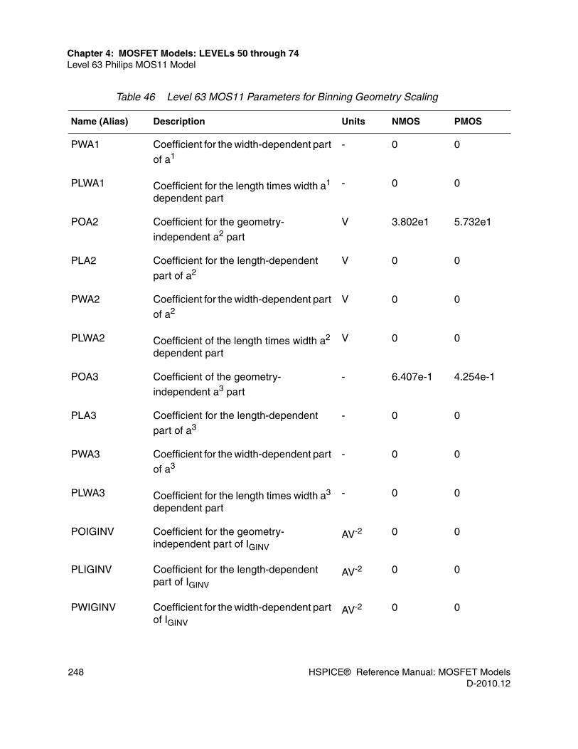
248 HSPICE® Reference Manual: MOSFET ModelsD-2010.12
Chapter 4: MOSFET Models: LEVELs 50 through 74Level 63 Philips MOS11 Model
PWA1 Coefficient for the width-dependent part
of a1- 0 0
PLWA1 Coefficient for the length times width a1 dependent part
- 0 0
POA2 Coefficient for the geometry-
independent a2 part
V 3.802e1 5.732e1
PLA2 Coefficient for the length-dependent
part of a2V 0 0
PWA2 Coefficient for the width-dependent part
of a2V 0 0
PLWA2 Coefficient of the length times width a2 dependent part
V 0 0
POA3 Coefficient of the geometry-
independent a3 part
- 6.407e-1 4.254e-1
PLA3 Coefficient for the length-dependent
part of a3- 0 0
PWA3 Coefficient for the width-dependent part
of a3- 0 0
PLWA3 Coefficient for the length times width a3 dependent part
- 0 0
POIGINV Coefficient for the geometry-independent part of IGINV
AV-2 0 0
PLIGINV Coefficient for the length-dependent part of IGINV
AV-2 0 0
PWIGINV Coefficient for the width-dependent part of IGINV
AV-2 0 0
Table 46 Level 63 MOS11 Parameters for Binning Geometry Scaling
Name (Alias) Description Units NMOS PMOS

HSPICE® Reference Manual: MOSFET Models 249D-2010.12
Chapter 4: MOSFET Models: LEVELs 50 through 74Level 63 Philips MOS11 Model
PLWIGINV Coefficient for the length times width dependent part of IGINV
AV-2 0 0
POBINV Coefficient for the geometry-independent part of IGINV
V 48 87.5
PLBINV Coefficient for the length-dependent part of IGINV
V 0 0
PWBINV Coefficient for the width-dependent part of IGINV
V 0 0
PLWBINV Coefficient for the length times width dependent part of IGINV
V 0 0
POIGACC Coefficient for the geometry-independent part of IGACC
AV-2 0 0
PLIGACC Coefficient for the length-dependent part of IGACC
AV-2 0 0
PWIGACC Coefficient for the width-dependent part of IGACC
AV-2 0 0
PLWIGACC Coefficient for the length times width dependent part of IGACC
AV-2 0 0
POBACC Coefficient for the geometry-independent part of BACC
V 48 48
PLBACC Coefficient for the length-dependent part of BACC
V 0 0
PWBACC Coefficient for the width-dependent part of BACC
V 0 0
PLWBACC Coefficient for the length times width dependent part of BACC
V 0 0
Table 46 Level 63 MOS11 Parameters for Binning Geometry Scaling
Name (Alias) Description Units NMOS PMOS

250 HSPICE® Reference Manual: MOSFET ModelsD-2010.12
Chapter 4: MOSFET Models: LEVELs 50 through 74Level 63 Philips MOS11 Model
VFBOV Flatband voltage for the source/drain overlap extensions
V 0 0
KOV Body-effect factor for the source/drain overlap extensions
V1/2 2.5 2.5
POIGOV Coefficient for the geometry-independent part of IGOV
AV-2 0 0
PLIGOV Coefficient for the length-dependent part of IGOV
AV-2 0 0
PWIGOV Coefficient for the width-dependent part of IGOV
AV-2 0 0
PLWIGOV Coefficient for the width over length dependent part of IGOV
AV-2 0 0
TOX Thickness of the gate oxide layer m 3.2e-9 3.2e-9
POCOX Coefficient for the geometry-independent COX part
F 2.98e-14 2.717e-14
PLCOX Coefficient for the length-dependent part of COX
F 0 0
PWCOX Coefficient for the width-dependent part of COX
F 0 0
PLWCOX Coefficient for the length times width dependent part of COX
F 0 0
POCGDO Coefficient for the geometry-independent CGDO part
F 6.392e-15 6.358e-15
PLCGDO Coefficient for the length-dependent part of CGDO
F 0 0
PWCGDO Coefficient for the width dependent part of CGDO
F 0 0
Table 46 Level 63 MOS11 Parameters for Binning Geometry Scaling
Name (Alias) Description Units NMOS PMOS

HSPICE® Reference Manual: MOSFET Models 251D-2010.12
Chapter 4: MOSFET Models: LEVELs 50 through 74Level 63 Philips MOS11 Model
PLWCGDO Coefficient for the width over length dependent part of CGDO
F 0 0
POCGSO Coefficient for the geometry-independent part of CGSO
F 6.392e-15 6.358e-15
PLCGSO Coefficient for the length-dependent part of CGSO
F 0 0
PWCGSO Coefficient for the width-dependent part of CGSO
F 0 0
PLWCGSO Coefficient for the width over length dependent part of CGSO
F 0 0
GATENOISE Inclusion/exclusion flag of the induced gate thermal noise
- 0 0
NT Coefficient for the thermal noise at the reference temperature
J 1.656e-20 1.656e-20
PONFA Coefficient for the geometry-independent NFA part
V-1m-4 8.323e22 1.90e22
PLNFA Coefficient for the length-dependent part of NFA
V-1m-4 0 0
PWNFA Coefficient for the width-dependent part of NFA
V-1m-4 0 0
PLWNFA Coefficient for the length times width dependent part of NFA
V-1m-4 0 0
PONFB Coefficient for the geometry-independent NFB part
V-1m-2 2.514e7 5.043e6
PLNFB Coefficient for the length-dependent part of NFB
V-1m-2 0 0
Table 46 Level 63 MOS11 Parameters for Binning Geometry Scaling
Name (Alias) Description Units NMOS PMOS

252 HSPICE® Reference Manual: MOSFET ModelsD-2010.12
Chapter 4: MOSFET Models: LEVELs 50 through 74Level 63 Philips MOS11 Model
PWNFB Coefficient for the width-dependent part of NFB
V-1m-2 0 0
PLWNFB Coefficient for the length times width dependent part of NFB
V-1m-2 0 0
PONFC Coefficient for the geometry-independent NFC part
V-1 0 3.627e-10
PLNFC Coefficient for the length-dependent part of NFC
V-1 0 0
PWNFC Coefficient for the width-dependent part of NFC
V-1 0 0
PLWNFC Coefficient for the length times width dependent part of NFC
V-1 0 0
POTVFB Coefficient for the geometry-independent part of ST;VFB
VK-1 5.0e-4 5.0e-4
PLTVFB Coefficient for the length-dependent part of ST;VFB
VK-1 0 0
PWTVFB Coefficient for the width-dependent part of ST;VFB
VK-1 0 0
PLWTVFB Coefficient for the length times width dependent part of ST;VFB
VK-1 0 0
POTPHIB Coefficient for the geometry-independent part of ST;φB
VK-1 -8.5e-4 -8.5e-4
PLTPHIB Coefficient for the length-dependent part of ST;φB
VK-1 0 0
PWTPHIB Coefficient for the width-dependent part of ST;φB
VK-1 0 0
Table 46 Level 63 MOS11 Parameters for Binning Geometry Scaling
Name (Alias) Description Units NMOS PMOS

HSPICE® Reference Manual: MOSFET Models 253D-2010.12
Chapter 4: MOSFET Models: LEVELs 50 through 74Level 63 Philips MOS11 Model
PLWTPHIB Coefficient for the length times width dependent part of ST;φB
VK-1 0 0
POTETABET Coefficient for the geometry-independent part of ηβ
- 1.30 0.5
PLTETABET Coefficient for the length-dependent part of ηβ
- 0 0
PWTETABET Coefficient for the width-dependent part of ηβ
- 0 0
PLWTETABET Coefficient for the length times width ηsr dependent part
- 0 0
POTETASR Coefficient for the geometry-independent ηsr part
- 0.65 0.5
PLTETASR Coefficient for the length-dependent part of ηsr
- 0 0
PWTETASR Coefficient for the width-dependent part of ηsr
- 0 0
PLWTETASR Coefficient for the length times width dependent part of ηsr
- 0 0
POTETAPH Coefficient for the geometry-independent ηph part
- 1.35 3.75
PLTETAPH Coefficient for the length-dependent part of ηph
- 0 0
PWTETAPH Coefficient for the width-dependent part of ηph
- 0 0
PLWTETAPH Coefficient for the length times width ηph dependent part
- 0 0
Table 46 Level 63 MOS11 Parameters for Binning Geometry Scaling
Name (Alias) Description Units NMOS PMOS

254 HSPICE® Reference Manual: MOSFET ModelsD-2010.12
Chapter 4: MOSFET Models: LEVELs 50 through 74Level 63 Philips MOS11 Model
POTETAMOB Coefficient for the geometry-independent part of ST:ηph
K-1 0 0
PLTETAMOB Coefficient for the length-dependent part of ηph
K-1 0 0
PWTETAMOB Coefficient for the width-dependent part of ηph
K-1 0 0
PLWTETAMOB Coefficient for the length times width dependent part of ηph
K-1 0 0
NU Exponent of the field dependence of the mobility model at the reference temperature
- 2 2
POTNUEXP Coefficient for the geometry-independent νexp part
- 5.25 3.23
PLTNUEXP Coefficient for the length-dependent part of νexp
- 0 0
PWTNUEXP Coefficient for the width-dependent part of νexp
- 0 0
PLWTNUEXP Coefficient fore the length times width dependent part of νexp
- 0 0
POTETAR Coefficient for the geometry-independent ηR part
- 0.95 0.4
PLTETAR Coefficient for the length-dependent part of ηR
- 0 0
PWTETAR Coefficient for the width-dependent part of ηR
- 0 0
PLWTETAR Coefficient for the length times width dependent part of ηR
- 0 0
Table 46 Level 63 MOS11 Parameters for Binning Geometry Scaling
Name (Alias) Description Units NMOS PMOS

HSPICE® Reference Manual: MOSFET Models 255D-2010.12
Chapter 4: MOSFET Models: LEVELs 50 through 74Level 63 Philips MOS11 Model
POTETASAT Coefficient for the geometry-independent part of ηsat
- 1.04 0.86
PLTETASAT Coefficient for the length-dependent part of ηsat
- 0 0
PWTETASAT Coefficient for the width-dependent part of ηsat
- 0 0
PLWTETASAT Coefficient for the length times width dependent part of ηsat
- 0 0
POTA1 Coefficient for the geometry-
independent ST:a1 partK-1 0 0
PLTA1 Coefficient for the length-dependent
part of ST:a1K-1 0 0
PWTA1 Coefficient for the width-dependent part
of ST:a1K-1 0 0
PLWTA1 Coefficient for the length times width
dependent part of ST:a1K-1 0 0
POAGIDL Coefficient for the geometry-independent part of AGIDL
AV-3 0 0
PLAGIDL Coefficient for the length dependence of AGIDL
AV-3 0 0
PWAGIDL Coefficient for the width dependence of AGIDL
AV-3 0 0
PLWAGIDL Coefficient for the width over length dependence of AGIDL
AV-3 0 0
POBGIDL Coefficient for the geometry independent part of BGIDL
V 41.0 41.0
Table 46 Level 63 MOS11 Parameters for Binning Geometry Scaling
Name (Alias) Description Units NMOS PMOS

256 HSPICE® Reference Manual: MOSFET ModelsD-2010.12
Chapter 4: MOSFET Models: LEVELs 50 through 74Level 63 Philips MOS11 Model
PLBGIDL Coefficient for the length dependence of BGIDL
V 0 0
PWBGIDL Coefficient for the width dependence of BGIDL
V 0 0
PLWBGIDL Coefficient for the length times width dependence of BGIDL
V 0 0
POCGIDL Coefficient for the geometry independent part of CGIDL
0 0
PLCGIDL Coefficient for the length dependence of CGIDL
0 0
PWCGIDL Coefficient for the width dependence of CGIDL
0 0
PLWCGIDL Coefficient for the length times width dependence of CGIDL
0 0
POTBGIDL Coefficient for the geometry independent part of ST:BGIDL
VK-1 -3.638e-4 -3.638e-4
PLTBGIDL Coefficient for the length dependence of ST:BGIDL
VK-1 0 0
PWTBGIDL Coefficient for the width dependence of ST:BGIDL
VK-1 0 0
PLWTBGIDL Coefficient for the length times width dependence of ST:BGIDL
VK-1 0 0
Table 46 Level 63 MOS11 Parameters for Binning Geometry Scaling
Name (Alias) Description Units NMOS PMOS

HSPICE® Reference Manual: MOSFET Models 257D-2010.12
Chapter 4: MOSFET Models: LEVELs 50 through 74Level 63 Philips MOS11 Model
The following are JUNCAP model parameters specifically for the Philips MOS 11 (Level 63) model.
Table 47 Level 63 JUNCAP Parameters
Name Description Units Default
DTA Temperature offset of the JUNCAP element with respect toTA ° C 0
VR Voltage at which simulation determines parameters V 0
JSGBR Bottom saturation-current density due to generating an electron hole at V=VR
Am-2 1e-03
JSDBR Bottom saturation-current density due to diffusion from back contact Am-2 1e-03
JSGSR Sidewall saturation-current density due to generating an electron hole at V=VR
Am-1 1e-03
JSDSR Sidewall saturation-current density due to back-contact diffusion Am-1 1e-03
JSGGR Gate edge saturation-current density due to generating an electron hole at V=VR
Am-1 1e-03
JSDGR Gate edge saturation-current density due to back-contact diffusion Am-1 1e-03
NB Emission coefficient of the bottom forward current - 1
NS Emission coefficient of the sidewall forward current - 1
NG Emission coefficient of the gate edge forward current - 1
CJBR Bottom junction capacitance at V=VR Fm-2 1e-12
CJSR Sidewall junction capacitance at V=VR Fm-1 1e-12
CJGR Gate edge junction capacitance at V=VR Fm-1 1e-12
VDBR Diffusion voltage of the bottom junction at T=TR V 1
VDSR Diffusion voltage of the sidewall junction at T=TR V 1
VDGR Diffusion voltage of the gate-edge junction at T=TR V 1

258 HSPICE® Reference Manual: MOSFET ModelsD-2010.12
Chapter 4: MOSFET Models: LEVELs 50 through 74Level 63 Philips MOS11 Model
Note: All symbols refer to “Unclassified Report NL-UR 2001/813”.
PB Bottom junction grading coefficient - 0.4
PS Sidewall junction grading coefficient - 0.4
PG Gate edge junction grading coefficient - 0.4
Table 47 Level 63 JUNCAP Parameters
Name Description Units Default

HSPICE® Reference Manual: MOSFET Models 259D-2010.12
Chapter 4: MOSFET Models: LEVELs 50 through 74Level 63 Philips MOS11 Model
Example 1.model nch nmos level=63+ VERSION=1100+ LER=1E-06 WER=1E-05 LAP=-1.864E-08+ TR=21 VFBR=-1.038 SLPHIB=-1.024E-08+ SL2PHIB=1.428E-14 KOR=5.763E-01 SLKO=2.649E-08+ SL2KO=-1.737E-14 KPINV=2.2E-01 PHIBR=0.85+ BETSQ=1.201E-04 ETABET=1.3 FBET1=-3.741000E-01+ LP1=2.806E-06 LP2=1E-10 THESATEXP=2+ THESRR=7.109E-01 THEPHR=1E-03 TOX=3.2E-09+ ETAPH=1.75E+00 ETAMOBR=2.825 NUR=1+ NUEXP=3.228 THERR=1.267E-01 ETAR=0.4+ THER2=1 THESATR=6.931E-02 SLTHESAT=1+ ETASAT=8.753E-01 SSFR=2.304E-03 VP=5E-02+ SLSSF=1.002E-06 ALPR=1.062E-02 SLALP=9.957E-01+ ALPEXP=1.039 THETHR=2.413E-03 THETHEXP=1+ SDIBLO=1.06E-06 SDIBLEXP=6.756 LLMIN=2E-07+ MOR=1.05E-03 MOEXP=3.146+ A1R=9.938E+04 STA1=9.3E-02 SLA1=-2.805E-03+ A2R=4.047E+01 SLA2=1E-15+ A3R=7.54E-01 SLA3=-8.705E-08+ COL=3.2E-10+ NTR=1.6237E-20 NFAR=1 NFBR=0+ NFCR=0 GATENOISE=0+ CJBR=1.347E-3 CJSR=0.183E-9 CJGR=0.374E-9+ JSDBR=0.027E-6 JSDSR=0.040E-12 JSDGR=0.100E-12+ VR=0.000+ JSGBR=1.900E-6 JSGSR=78.000E-12 JSGGR=54.000E-12+ VB=20.000+ VDBR=0.828 VDSR=0.593 VDGR=0.500+ PB=0.394 PS=0.171 PG=0.193+ NB=1.000 NS=1.000 NG=1.000

260 HSPICE® Reference Manual: MOSFET ModelsD-2010.12
Chapter 4: MOSFET Models: LEVELs 50 through 74Level 63 Philips MOS11 Model
Example 2.model nch nmos level=63+ VERSION=11010 + LVAR=0.000000E+00 + LAP=-1.864000E-08 WVAR=0.000000E+00 WOT=0.000000E+00 + TR=2.100000E+01 VFB=-1.038000E+00 STVFB=0.000000E+00 + SLPHIB=-1.024000E-08 SL2PHIB=1.428000E-14 SWPHIB=0.000000E+00 + KOR=5.763000E-01 SLKO=2.649000E-08 SL2KO=-1.737000E-14 + SWKO=0.000000E+00 KPINV=2.200000E-01 PHIBR=8.500000E-01 + BETSQ=1.201000E-04 ETABETR=1.300000E+00 FBET1=-3.741000E-01 + LP1=2.806000E-06 FBET2=0.000000E+00 LP2=1.000000E-10 + THESRR=7.109000E-01 SWTHESR=0.000000E+00 THEPHR=1.000000E-03 + ETAPH=1.750000E+00 SWTHEPH=0.000000E+00 ETAMOBR=2.825000E+00 + STETAMOB=0.000000E+00 SWETAMOB=0.000000E+00 NU=1.000000E+00 + NUEXP=3.228000E+00 THERR=1.267000E-01 ETAR=4.000000E-01 + SWTHER=0.000000E+00 THER1=0.000000E+00 THER2=1.000000E+00 + THESATR=6.931000E-02 SLTHESAT=1.000000E+00 THESATEXP=2.000000E+00 + ETASAT=8.753000E-01 SWTHESAT=0.000000E+00 SSFR=2.304000E-03 + SLSSF=1.002000E-06 SWSSF=0.000000E+00 ALPR=1.062000E-02 + SLALP=9.957000E-01 ALPEXP=1.039000E+00 SWALP=0.000000E+00 + VP=5.000000E-02 THETHR=2.413000E-03 THETHEXP=1.000000E+00 + SWTHETH=0.000000E+00 SDIBLO=1.060000E-06 SDIBLEXP=6.756000E+00 + MOR=1.050000E-03 MOEXP=3.146000E+00 LLMIN=2.000000E-07 + A1R=9.938000E+04 STA1=9.300000E-02 SLA1=-2.805000E-03 + SWA1=0.000000E+00 A2R=4.047000E+01 SLA2=1.000000E-15 + SWA2=0.000000E+00 A3R=7.540000E-01 SLA3=-8.705000E-08 + SWA3=0.000000E+00 TOX=3.200000E-09 COL=3.200000E-10 + NT=1.623700E-20 NFAR=1.000000E-00 NFBR=0.000000E+00 + NFCR=0.000000E+00 GATENOISE =0.00000E-00 DTA=0.000000E-00

HSPICE® Reference Manual: MOSFET Models 261D-2010.12
Chapter 4: MOSFET Models: LEVELs 50 through 74Level 64 STARC HiSIM Model
Example 3.model nch nmos level=63+ LEVEL =63 + VERSION=11011 + LVAR=0 LAP=4.0E-08 WVAR=0.0 WOT=0.0 TR=21 VFB=-0.105E+01+ POKO=0.5 PLKO=0.0 PWKO=0.0 PLWKO=0.0 KPINV=0.0 + POPHIB=0.95 PLPHIB=0.0 PWPHIB=0.0 POBET=1.922E-03+ POTHESR=3.562E-01 POTHEPH=1.29E-02 POETAMOB=1.4 POTHER=8.120E-02+ THER1=0.0 THER2=0.1E+01 POTHESAT=0.2513 POTHETH =1.0E-5 + POSDIBL=8.530E-4 POSSF=1.2E-2 POALP=2.5E-2 VP=5.0E-2 + POMEXP=0.2 POA1=6.022 POA2=38.02 POA3=0.6407 + POBINV=48 POBACC=48 KOV=2.5 TOX=3.2E-09+ POCOX=2.980E-14 POCGDO=6.392E-15 POCGSO=6.392E-15 + NT=1.656E-20 PONFA=8.323E+22 PONFB=2.514E+7 + POTVFB=5.0E-4 POTPHIB=-8.5E-4+ POTETABET=1.30 POTETASR=0.65 POTETAPH=1.350 NU=2.0+ POTNUEXP=5.25 POTETAR=0.95 POTETASAT=1.040
Level 64 STARC HiSIM Model
Note: See Level 68 STARC HiSIM2 Model for the latest version of this model.
HiSIM (Hiroshima-university STARC IGFET Model) is a publicly-available MOSFET model for circuit simulation. It uses drift-diffusion approximation, and a channel-surface-potential description. You can model all MOSFET characteristics closely, based on their physical origins by using fewer model parameters (about 90 model parameters); each parameter set is sufficient for all gate lengths. These model parameters are directly related to the MOSFET physics that a simulator can easily extract according to its physical meanings.
The STARC HiSIM model is Level 64 in the Synopsys MOSFET models. To use this model, specify:
M1 drain gate source bulk NCH w=4u l=1u.MODEL NCH NMOS LEVEL=64
HSPICE HiSIM model code is based on the Spice3f5 version that Hiroshima University/STARC released at the following web site:
http://www.starc.jp/index-j.html

262 HSPICE® Reference Manual: MOSFET ModelsD-2010.12
Chapter 4: MOSFET Models: LEVELs 50 through 74Level 64 STARC HiSIM Model
Since the STARC HiSIM1.1.0 release, the Synopsys version of the HiSIM model has included a VERSION number parameter to facilitate backward compatibility. Starting in the 2003.03 release, Synopsys uses the STARC version control mechanism so you must enter an integer for the VERSION model parameter. For example, to specify HiSIM version 1.0.0, set the VERSION model parameter to 100. If you do not set the VERSION parameter, simulation issues a warning and automatically sets this parameter to 100.
You can set the VERSION value to:■ 100, 101, 102 (HiSIM1.0.* series)■ 110, 111, 112 (HiSIM1.1.* series)■ 120 (HiSIM1.2.*)
Table 48 Level 64 Model Selectors
Parameter Default Description
LEVEL 64 Model selector
VERSION 100 Model version number
CORSRD 0(no) Flag. Indicates whether to include the Rs and Rd contact resistors, and whether to solve equations iteratively. CORSRD=1(yes)
COOVLP 0 Overlap capacitance model selector.■ COOVLP=-1, constant value■ COOVLP=0, approximating the field linear reduction ■ COOVLP=1, considering the lateral impurity profile.
COISUB 0 Substrate current model selector.■ for VERSION < 110, COISUB=0 (yes),■ otherwise, COISUB=1 (no)
COIIGS 0 Selects the gate tunneling current model.■ COIIGS=0 (yes),■ COIIGS=1 (no)
VERSION < 111 does not support this model.

HSPICE® Reference Manual: MOSFET Models 263D-2010.12
Chapter 4: MOSFET Models: LEVELs 50 through 74Level 64 STARC HiSIM Model
COGIDL 0 Selects the gate induced drain leakage (GIDL) current model.■ COGIDL=0 (yes)■ COGIDL=1 (no)
VERSION < 111 does not support this model.
CONOIS 0 1/f noise model selector.■ CONOIS=0 (no)■ CONOIS=1 (yes)
COISTI 0 Selects the shallow-trench-isolation (STI) leakage current.■ COISTI=0 (no)■ COISTI=1 (yes), only if VERSION ≥ 110.
NOISE 5 Channel thermal and flicker noises combination selector.■ NOISE=1
Channel thermal noise=SPICE2 modelFlicker noise=SPICE2 model
■ NOISE=2Channel thermal noise=HiSIM1 model for the BSIM3 modelFlicker noise=HiSIM1 model
■ NOISE=3Channel thermal noise=SPICE2 modelFlicker noise=HiSIM1 model
■ NOISE=4Channel thermal noise=HiSIM1 model for the BSIM3 modelFlicker noise=SPICE2 model
■ NOISE=5Channel thermal noise=NONEFlicker noise=HiSIM1 model
Table 48 Level 64 Model Selectors
Parameter Default Description

264 HSPICE® Reference Manual: MOSFET ModelsD-2010.12
Chapter 4: MOSFET Models: LEVELs 50 through 74Level 64 STARC HiSIM Model
Table 49 Level 64 Technological Parameters
Parameter Default Description
TOX 3.6e-9m Oxide thickness
XLD 0.0m Gate-overlap length
XWD 0.0m Gate-overlap width
XPOLYD 0.0m Difference between the gate-poly and the design lengths
TPOLY 0.0m Height of the gate poly-Si
RS 0.0ohm*m Source-contact resistance
RD 0.0ohm*m Drain-contact resistance
NSUBC 5.94e+17cm-3 Substrate-impurity concentration
NSUBP 5.94e+17cm-3 Maxim pocket concentration
VFBC -0.722729V Flat-band voltage
LP 0.0m Pocket penetration length
XJ 0.0m Junction depth (if VERSION < 110)
XQY 0.0m Distance from the drain junction to the maximum electric field point (if VERSION ≥ 110)
Table 50 Level 64 Temperature Dependence Parameters
Parameter Default Description
BGTMP1 9.03e-5eVK-1 Bandgap narrowing
BGTMP2 3.05e-7eVK-2 Bandgap narrowing

HSPICE® Reference Manual: MOSFET Models 265D-2010.12
Chapter 4: MOSFET Models: LEVELs 50 through 74Level 64 STARC HiSIM Model
Table 51 Level 64 Quantum Effect Parameters
Parameter Default Description
QME1 0.0mV Coefficient for the quantum mechanical effect
QME2 0.0V Coefficient for the quantum mechanical effect
QME3 0.0m Coefficient for the quantum mechanical effect
Table 52 Level 64 Poly Depletion Parameters
Parameter Default Description
PGD1 0.0V Strength of the poly depletion
PGD2 0.0V Threshold voltage of the poly depletion
PGD3 0.0 Vds dependence of the poly depletion
Table 53 Level 64 Short Channel Parameters
Parameter Default Description
PARL1 1.0 Strength of the lateral-electric-field gradient
PARL2 2.2e-8m Depletion width of the channel/contact junction
SC1 13.5V-1 Short-channel coefficient 1
SC2 1.8V-2 Short-channel coefficient 2
SC3 0.0V-2m Short-channel coefficient 3
SCP1 0.0V-1 Short-channel coefficient 1 for the pocket
SCP2 0.0V-2 Short-channel coefficient 2 for the pocket
SCP3 0.0V-2m Short-channel coefficient 3 for the pocket

266 HSPICE® Reference Manual: MOSFET ModelsD-2010.12
Chapter 4: MOSFET Models: LEVELs 50 through 74Level 64 STARC HiSIM Model
Table 54 Level 64 Narrow Channel Parameters
Parameter Default Description
WFC 0.0m*F/cm2 Voltage reduction
MUEPH2 0.0 Mobility reduction
W0 0.0log(cm) Minimum gate width
WVTHSC 0.0 Short-channel effect at the shallow-trench-isolation (STI) edge, if VERSION ≥ 110
NSTI 0.0cm-3 Substrate-impurity concentration at the shallow-trench-isolation (STI) edge, if VERSION ≥ 110
WSTI 0.0m Width of the high-field region at the shallow-trench-isolation (STI), if VERSION ≥ 110
Table 55 Level 64 Mobility Parameters
Parameter Default Description
VDS0 0.05V Drain voltage for extracting low-field mobility
MUECB0 300.0cm2/Vs Coulomb scattering
MUECB1 30.0cm2/Vs Coulomb scattering
MUEPH0 0.295 Phonon scattering
MUEPH1 1.0e7 Phonon scattering
MUETMP 0.0 Temperature dependence of phonon scattering
MUESR0 1.0 Surface-roughness scattering
MUESR1 7.0e8 Surface-roughness scattering
NDEP 1.0 Coefficient of the effective-electric field
NINV 0.5 Coefficient of the effective-electric field
NINVD 0.0V-1 Modification of NINV

HSPICE® Reference Manual: MOSFET Models 267D-2010.12
Chapter 4: MOSFET Models: LEVELs 50 through 74Level 64 STARC HiSIM Model
BB 2.0(NMOS)1.0(PMOS)
High-field-mobility degradation
VMAX 1.0e7cm/s Maximum saturation velocity
VOVER 0.0 Velocity overshoot effect
VOVERP 0.0 Lgate dependence of the velocity overshoot
RPOCK1 0.0V2*m1/2/A Resistance coefficient caused by the potential barrier
RPOCK2 0.0V Resistance coefficient caused by the potential barrier
RPOCP1 0.0 Resistance coefficient caused by the potential barrier, if VERSION ≥ 110
RPOCP2 0.0 Resistance coefficient caused by the potential barrier, if VERSION ≥ 110
Table 56 Level 64 Channel Length Modulation Parameters
Parameter Default Description
CLM1 0.3 Hardness coefficient of the channel/contact junction
CLM2 0.0 Coefficient for the QB contribution
CLM3 0.0 Coefficient for the QI contribution
Table 57 Level 64 Substrate Current Parameters
Parameter Default Description
SUB1 0.0V-1 Substrate current coefficient 1
SUB2 -70.0 Substrate current coefficient 2
SUB3 1.0 Substrate current coefficient 3
Table 55 Level 64 Mobility Parameters
Parameter Default Description

268 HSPICE® Reference Manual: MOSFET ModelsD-2010.12
Chapter 4: MOSFET Models: LEVELs 50 through 74Level 64 STARC HiSIM Model
Table 58 Level 64 Gate Current Parameters
Parameter Default Description
GLEAK1 0.0A*V-3/2/C Gate current coefficient 1
GLEAK2 0.0 Gate current coefficient 2
GLEAK3 0.0 Gate current coefficient 3
Table 59 Level 64 GIDL Current Parameters
Parameter Default Description
GIDL1 0.0A*m*V-3/2/C GIDL current coefficient 1
GIDL2 0.0V-1/2/cm GIDL current coefficient 2
GIDL3 0.0 GIDL current coefficient 3
Table 60 Level 64 1/f Noise Parameters
Parameter Default Description
NFALP 2.0e-15 Contribution of the mobility fluctuation
NFTRP 1.0e11 Ratio of trap density to the attenuation coefficient
CIT 0.0F/cm2 Capacitance caused by the interface trapped carriers
AF 1.0 SPICE2 flicker noise exponent
KF 0.0 SPICE2 flicker noise coefficient
EF 0.0 SPICE2 flicker noise frequency exponent
Table 61 Conserving Symmetry at Vds=0 for Short-Channel MOSFETS
Parameter Default Description
VZADD0 1.0e-2V Symmetry conservation coefficient

HSPICE® Reference Manual: MOSFET Models 269D-2010.12
Chapter 4: MOSFET Models: LEVELs 50 through 74Level 64 STARC HiSIM Model
PZADD0 1.0e-3V Symmetry conservation coefficient
Table 62 MOS DIODE
Parameter Default Description
JSO 1.0e-4Am-2 Saturation current density
JSOSW 0.0Am-1 Sidewall saturation current density
NJ 1.0 Emission coefficient
NJSW 1.0 Sidewall emission coefficient
XTI 3.0 Junction current temperature exponent coefficient
CJ 8.397247e-04Fm-2 Bottom junction capacitance per unit area at zero bias
CJSW 5.0e-10Fm-1 Source/drain sidewall junction capacitance per unit area at zero bias
CJSWG 5.0e-10Fm-1 Source/drain gate sidewall junction capacitance per unit area at zero bias
MJ 0.5 Bottom junction capacitance grading coefficient
MJSW 0.33 Source/drain sidewall junction capacitance grading coefficient
MJSWG 0.33 Source/drain gate sidewall junction capacitance grading coefficient
PB 1.0V Bottom junction build-in potential
PBSW 1.0V Source/drain sidewall junction build-in potential
PBSWG 1.0V Source/drain gate sidewall junction build-in potential
Table 61 Conserving Symmetry at Vds=0 for Short-Channel MOSFETS
Parameter Default Description

270 HSPICE® Reference Manual: MOSFET ModelsD-2010.12
Chapter 4: MOSFET Models: LEVELs 50 through 74Level 64 STARC HiSIM Model
Note: Model parameter defaults in the above tables are valid only for versions 100 and 110. For other versions, please refer to the following table:
VDIFFJ 0.5V Diode threshold voltage between source/drain and substrate
Table 63 Subthreshold Swing
Parameter Default Description
PTHROU 0.0 Correction for steep subthreshold swing
Table 64 Model Parameter Version Defaults
Parameter Version=100, 110 Others
VMAX 1.00e+7 7.00e+6
BGTMP1 9.03e-5 90.25e-6
BGTMP2 3.05e-7 100.0e-9
TOX 3.60e-9 5.0e-9
RS 0.0 80.0e-6
RD 0.0 80.0e-6
VFBC -0.722729 -1.0
NSUBC 5.94e+17 1.0e+17
PARL2 2.20e-8 1.0e+17
LP 0.0 15.0e-9
NSUBP 5.94e+17 1.0e+17
SC1 13.5 0.0
Table 62 MOS DIODE
Parameter Default Description

HSPICE® Reference Manual: MOSFET Models 271D-2010.12
Chapter 4: MOSFET Models: LEVELs 50 through 74Level 64 STARC HiSIM Model
SC2 1.8 0.0
PGD1 0.0 0.01
PGD2 0.0 1.0
PGD3 0.0 0.8
NINVD 0.0 1.0e-9
MUEPH1 1.00e+7 25.0e+3
MUEPH0 0.295 0.300
MUESR1 7.00e+8 2.0e+15
MUESR0 1.0 2.0
MUETMP 0.0 1.5
SUB1 0.0 10.0
SUB2 -70.0 20.0
SUB3 1.0 0.8
CJ 8.397247e-04 5.0e-04
CLM1 0.3 0.7
CLM2 0.0 2.0
CLM3 0.0 1.0
RPOCK1 0.0 0.01
RPOCK2 0.0 0.1
RPOCP1 0.0 1.0
VOVER 0.0 0.01
Table 64 Model Parameter Version Defaults
Parameter Version=100, 110 Others

272 HSPICE® Reference Manual: MOSFET ModelsD-2010.12
Chapter 4: MOSFET Models: LEVELs 50 through 74Level 64 STARC HiSIM Model
To turn off the model effects, use the following settings:■ Short-Channel Effect SC1=SC2=SC3=0■ Reverse-Short-Channel Effect LP=0■ Quantum-Mechanical Effect QME1=QME2=QME3=0■ Poly-Depletion Effect PGD1=PGD2=PGD3=0■ Channel-Length Modulation CLM1=CLM2=CLM3=0■ Narrow-Channel Effect WFC=MUEPH2=0
VOVERP 0.0 0.1
QME1 0.0 40.0e-12
QME2 0.0 300.0e-12
GIDL1 0.0 5.0e-3 for HiSIM101, 5.0e-6 for others
GIDL2 0.0 1.0e+6
GIDL3 0.0 0.3
GLEAK1 0.0 0.01e+6 for HiSIM101, 10.0e+3 for others
GLEAK2 0.0 20.0e+6
GLEAK3 0.0 0.3
PZADD0 1.0e-3 5.0e-3
NFTRP 100.0e+9 10.0e+9
NFALP 2.00e-15 1.0e-16
Table 64 Model Parameter Version Defaults
Parameter Version=100, 110 Others

HSPICE® Reference Manual: MOSFET Models 273D-2010.12
Chapter 4: MOSFET Models: LEVELs 50 through 74Level 68 STARC HiSIM2 Model
Level 68 STARC HiSIM2 Model
HiSIM (Hiroshima University/STARC IGFET Model) is the first complete surface-potential-based MOSFET model for circuit simulation. The most important advantage of the surface-potential-based modeling is the unified description of device characteristics for all bias conditions. The physical reliability of the drift-diffusion approximation has been proved by 2-D device simulations with channel lengths below 0.1um.
Note: HiSIM2 source code, and all copyrights, trade secrets or other intellectual property rights in and to the source code in its entirety, is owned by Hiroshima University and STARC.
The following sections discuss these topics:■ HiSIM Version 2.3.1■ Level 68 HiSIM Model v2.4.1, 2.4.2, 2.4.3, and 2.5.0■ Updates Based on HiSIM 2.4.1■ Updates Based on HiSIM 2.4.2■ Updates Based on HiSIM 2.4.3■ Updates Based on HiSIM 2.5.0
HiSIM Version 2.3.1The STARC HiSIM2 is Level 68 in the Synopsys MOSFET models. HiSIM2.3.1 is an improved version that resolved many issues of previous releases.
HiSIM version 2.3.1 provides:■ Improved Linear Region Modeling■ Improved Small Size Model■ Improved Isub Model■ Inclusion of Induced Gate Noise■ Support for DFM (Interface to Instance Parameters)

274 HSPICE® Reference Manual: MOSFET ModelsD-2010.12
Chapter 4: MOSFET Models: LEVELs 50 through 74Level 68 STARC HiSIM2 Model
Level 68 HiSIM Model v2.4.1, 2.4.2, 2.4.3, and 2.5.0To obtain analytical solutions for describing device performances, the charge sheet approximation of the inversion layer with zero thickness has been introduced. Together with the gradual-channel approximation all device characteristics are then described analytically by the channel-surface potentials at the source side and at the drain side. These surface potentials are functions of applied voltages on the four MOSFET terminals; the gate voltage Vg, the drain voltage Vd, the bulk voltage Vb and the reference potential of the source Vs. This is the long-channel basis of the HiSIM model, and extensions of the model approximations are done for advanced technologies. All newly appearing phenomena such as short-channel and reverse-short-channel effects are included in the surface potential calculations causing modifications resulting from the features of these advanced technologies. See also: Updates Based on HiSIM 240SC2, Updates Based on HiSIM 2.4.1, Updates Based on HiSIM 2.4.2, Updates Based on HiSIM 2.4.3, and Updates Based on HiSIM 2.5.0.
For details and usage, contact the Synopsys support team.
The following sections describe these topics:■ General Syntax for the HiSIM241 Model■ Listing of Instance Parameters for HiSIM 2.4.1■ Updates Based on HiSIM 240SC2
General Syntax for the HiSIM241 ModelThe following lists and describes the HiSIM Level 68 general parameters.
Mxxx nd ng ns [nb] mname [L=val] [W=val] [M=val]+ [AD=val] [AS=val] [PD=val] [PS=val]+ [NRS=val] [NRD=val] [XGW=val] [XGL=val]+ [NF=val] [NGCON=val] [RBPB=val] [RBPD=val]+ [RBPS=val] [RBDB=val] [RBSB=val] [SA=val]+ [SB=val] [SD=val] [TEMP=val] [DTEMP=val]+ [NSUBCDFM=val]
.MODEL MNAME N(P)MOS LEVEL=68 VERSION=240.0+ [CORSRD=val] [COOVLP=val] [COISUB=val]+ [COIIGS=val] [COGIDL=val] [COISTI=val]+ [COADOV=val] [CONQS=val] [CORG=val] [CORBNET=val]+ [COFLICK=val] [COTHRML=val] [COIGN=val] [COIPRV=val]

HSPICE® Reference Manual: MOSFET Models 275D-2010.12
Chapter 4: MOSFET Models: LEVELs 50 through 74Level 68 STARC HiSIM2 Model
+ [COPPRV=val] [CODFM=val] + ... ... ... ... ...
The following tables list parameters that have been updated to the HiSIM 240 SC2 release.
Table 65 HiSIM Level 68 General Parameters
Parameter Description
CORSRD=val The following flags are prepared to select required model options.■ 0: no (default)■ 1 : yes, as internal resistances of HiSIM■ 2 : yes, analytical description■ 3 yes, both internal and analytical descriptions■ -1 : yes, as external resistances of HiSIM
COOVLP=val Overlap capacitance model is selected as:■ 0: constant overlap capacitance■ 1: (yes, default)
COISUB =val Substrate current Isub is calculated:■ 0: no (default)■ 1: yes
COIIGS = val Gate current Igate is calculated:■ 0: no (default)■ 1: yes
COGIDL = val GIDL current IGIDL is calculated:■ 0: no (default)■ 1: yes
COISTI = val STI leakage current Ids, STI is calculated:■ 0: no (default)■ 1: yes
COADOV = val Lateral field induced and overlap charges/capacitances are added to intrinsic ones:■ 0: no■ 1: yes (default)
& RS RD⁄ 0≠&RD 0≠&RD 0≠
RS RD⁄ 0≠

276 HSPICE® Reference Manual: MOSFET ModelsD-2010.12
Chapter 4: MOSFET Models: LEVELs 50 through 74Level 68 STARC HiSIM2 Model
CONQS = val Non-quasi-static mode is invoked:■ 0: no (default)■ 1: yes
CORG = val Gate-contact resistance is included (This flag can also be given as an instance parameter):■ 0: no (default)■ 1: yes
CORBNET = val Substrate resistance network is invoked (This flag can also be given as a instance parameter):■ 0: no (default)■ 1: yes
COFLICK = val 1/f noise is calculated:■ 0: no (default)■ 1: yes
COTHRML = val Thermal noise is calculated:■ 0: no (default)■ 1: yes
COIGN = val Induced gate and cross correlation noise are calculated:■ 0 || COTHRML = 0: no (default)■ 1 & COTHRML = 1: yes
COIPRV = val Previous Ids is used for calculating source/drain resistance effect (Rs and/or ):■ 0: no■ 1: yes (default)
COPPRV = val Previous s is used for the iteration:■ 0: no■ 1: yes (default)
CODFM = val Parameter variations for the DFM support is considered:■ 0: no (default)■ 1: yes
Table 65 HiSIM Level 68 General Parameters
Parameter Description
Rd 0•
∅

HSPICE® Reference Manual: MOSFET Models 277D-2010.12
Chapter 4: MOSFET Models: LEVELs 50 through 74Level 68 STARC HiSIM2 Model
Listing of Basic Device Parameters
.
COSELFHEAT =val ■ 0: no (default)■ 1: yes
Table 66 Basic Device Parameters
Parameter Description
TOX Physical oxide thickness
XL Difference between real and drawn gate length
XW Difference between real and drawn gate width
XLD Gate-overlap in length
XWD Gate-overlap in width
TPOLY Height of the gate poly-Si for fringing capacitance
LL Coefficient of gate length modification
LLD Coefficient of gate length modification
LLN Coefficient of gate length modification
WL Coefficient of gate width modification
WLD Coefficient of gate width modification
WLN Coefficient of gate width modification
NSUBC Substrate-impurity concentration
NSUBP Maximum pocket concentration
LP Pocket penetration length
*NPEXT Maximum concentration of pocket tail
Table 65 HiSIM Level 68 General Parameters
Parameter Description

278 HSPICE® Reference Manual: MOSFET ModelsD-2010.12
Chapter 4: MOSFET Models: LEVELs 50 through 74Level 68 STARC HiSIM2 Model
*LPEXT Extension length of pocket tail
VFBC Flat-band voltage
VBI Built-in potential
KAPPA Dielectric constant for gate dielectric
EG0 Bandgap
BGTMP1 Temperature dependence of bandgap
BGTMP2 Temperature dependence of bandgap
TNOM Temperature selected as nominal temperature value
Table 67 Velocity
Parameter Description
VMAX Saturation velocity
VOVER Velocity overshoot effect
VOVERP Leff dependence of velocity overshoot
*VTMP Temperature dependence of the saturation velocity
Table 68 Quantum-Mechanical Effects
Parameter Description
QME1 Vgs dependence
QME2 Vgs dependence
QME3 Minimum Tox modification
Table 66 Basic Device Parameters
Parameter Description

HSPICE® Reference Manual: MOSFET Models 279D-2010.12
Chapter 4: MOSFET Models: LEVELs 50 through 74Level 68 STARC HiSIM2 Model
HSPICE prints mobility parameters for Level 68.
Table 69 Poly-Silicon Depletion Effects
Parameter Description
PGD1 Strength of poly depletion
PGD2 Threshold voltage of poly depletion
PGD3 Vds dependence of poly depletion
*PGD4 Lgate dependence of poly depletion
Table 70 Short Channel Effect
Parameter Description
PARL2 Depletion width of channel/contact junction
SC1 Magnitude of short-channel effect
SC2 Vds dependence of short-channel effect
*SC3 Vbs dependence of short-channel effect
SCP1 Magnitude of short-channel effect due to pocket
SCP2 Vds dependence of short-channel due to pocket
*SCP3 Vbs dependence of short-channel effect due to pocket
*SCP21 Short-channel-effect modification for small Vds
*SCP22 Short-channel-effect modification for small Vds
*BS1 Body-coefficient modification due to impurity profile
*BS2 Body-coefficient modification due to impurity profile
Table 71 Mobility Model
Parameter Description
MUECB0 Coulomb scattering

280 HSPICE® Reference Manual: MOSFET ModelsD-2010.12
Chapter 4: MOSFET Models: LEVELs 50 through 74Level 68 STARC HiSIM2 Model
MUECB1 Coulomb scattering
MUEPH0 Phonon scattering
MUEPH1 Phonon scattering
*MUEPHL Length dependence of phonon mobility reduction
*MUEPHP Length dependence of phonon mobility reduction
MUESR0 Surface roughness scattering
MUESR1 Surface roughness scattering
*MUESRL Length dependence of surface roughness mobility reduction
*MUESLP Length dependence of surface roughness mobility reduction
NDEP Depletion charge contribution on effective-electric filed
*NDEPL Modification of depletion charge contribution for short-channel case
*NDEPLP Modification of depletion charge contribution for short-channel case
NINV Inversion charge of depletion charge contribution for short-channel case
BB High-filed-mobility degradation
VOVERP Leff dependence of velocity overshoot
Table 72 Channel-Length Modulation
Parameter Description
CLM1 Hardness coefficient of channel/contact junction
CLM2 Coefficient for contribution
CLM3 Coefficient for contribution
CLM4 No longer used
Table 71 Mobility Model (Continued)
Parameter Description
QB
QI

HSPICE® Reference Manual: MOSFET Models 281D-2010.12
Chapter 4: MOSFET Models: LEVELs 50 through 74Level 68 STARC HiSIM2 Model
*CLM5 Effect of pocket implantation
*CLM6 Effect of pocket implantation
Table 73 Narrow Channel Effects
Parameter Description
WFC Threshold voltage change due to capacitance change
*WVTH0 Threshold voltage drift
*NSUBP0 Modification of pocket concentration for narrow width
*NSUBWP Modification of pocket concentration for narrow width
*MUEPHW Phonon-related mobility reduction
*MUEPHP Phonon-related mobility reduction
*MUESRW Change of surface roughness related mobility
*MUESRW Change of surface roughness related mobility
*VTHSTI Threshold voltage shift due to STI
*VDSTI Vds dependence of threshold voltage shift due to STI
*SCSTI1 The same effect as SC1 but at STI edge
*SCSTI2 The same effect as SC2 but at STI edge
SCSTI3 No longer use
NSTI Substrate impurity concentration at STI edge
WSTI Width of the high-field region at STI edge
*WSTIL Channel-width dependence of WSTI
*WSTILP Channel-width dependence of WSTI
Table 72 Channel-Length Modulation (Continued)
Parameter Description

282 HSPICE® Reference Manual: MOSFET ModelsD-2010.12
Chapter 4: MOSFET Models: LEVELs 50 through 74Level 68 STARC HiSIM2 Model
*WSTILW Channel-width dependence of WSTI
*WSTIWP Channel-width dependence of WSTI
WL1 Threshold voltage shift of STI leakage due to small size effect
WL1P Threshold voltage shift of STI leakage due to small size effect
NSUBPSTI1 Pocket concentration change due to diffusion-region length between gate and STI
NSUBPSTI2 Pocket concentration change due to diffusion-region length between gate and STI
NSUBPSTI3 Pocket concentration change due to diffusion-region length between gate and STI
MUESTI1 Mobility change due to diffusion-region length between gate and STI
MUESTI2 Mobility change due to diffusion-region length between gate and STI
MUESTI3 Mobility change due to diffusion-region length between gate and STI
SAREF Length of diffusion between gate and STI
SBREF Length of diffusion between gate and STI
Table 74 Small Size Effect
Parameter Description
WL2 Threshold voltage shift due to small size effect
WL2P Threshold voltage shift due to small size effect
*MUEPHS Mobility modification due to small size
*MUEPSP Mobility modification due to small size
*VOVERS Modification of maximum velocity due to small size
*VOVERSP Modification of maximum velocity due to small size
Table 73 Narrow Channel Effects (Continued)
Parameter Description
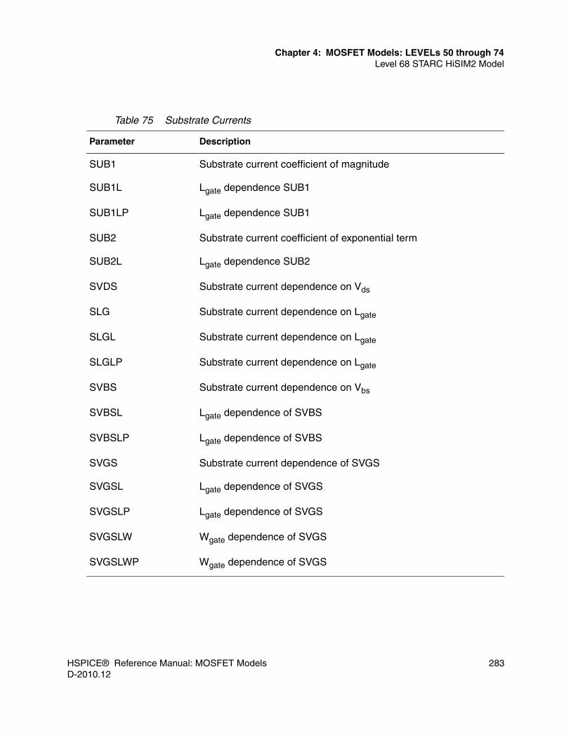
HSPICE® Reference Manual: MOSFET Models 283D-2010.12
Chapter 4: MOSFET Models: LEVELs 50 through 74Level 68 STARC HiSIM2 Model
Table 75 Substrate Currents
Parameter Description
SUB1 Substrate current coefficient of magnitude
SUB1L Lgate dependence SUB1
SUB1LP Lgate dependence SUB1
SUB2 Substrate current coefficient of exponential term
SUB2L Lgate dependence SUB2
SVDS Substrate current dependence on Vds
SLG Substrate current dependence on Lgate
SLGL Substrate current dependence on Lgate
SLGLP Substrate current dependence on Lgate
SVBS Substrate current dependence on Vbs
SVBSL Lgate dependence of SVBS
SVBSLP Lgate dependence of SVBS
SVGS Substrate current dependence of SVGS
SVGSL Lgate dependence of SVGS
SVGSLP Lgate dependence of SVGS
SVGSLW Wgate dependence of SVGS
SVGSLWP Wgate dependence of SVGS

284 HSPICE® Reference Manual: MOSFET ModelsD-2010.12
Chapter 4: MOSFET Models: LEVELs 50 through 74Level 68 STARC HiSIM2 Model
Table 76 Subthreshold Swing
Parameter Description
*PTHOU Correction for subthreshold swing
Table 77 Impact- Ionization Induced Bulk Potential Change
Parameter Description
IBPC1 Impact-ionization induced bulk potential change
IBPC2 Impact-ionization induced bulk potential change
Table 78 Gate Leakage Current
Parameter Description
GLEAK1 Gate to channel current coefficient
GLEAK2 Gate to channel current coefficient
GLEAK3 Gate to channel current coefficient
GLEAK4 Gate to channel current coefficient
*GLEAK5 Gate to channel current coefficient (short channel correction)
*GLEAK6 Gate to channel current coefficient (Vds dependence correction)
*GLEAK7 Gate to channel current coefficient (gate length and width dependence correction)
*EGIG Bandgap of gate leakage
*IGTEMP2 Temperature dependence of gate leakage
*IGTEMP3 Temperature dependence of gate leakage
GLKB1 Gate to bulk current coefficient
GLKB2 Gate to bulk current coefficient
GLKB3 Flat-band shift for gate to bulk current

HSPICE® Reference Manual: MOSFET Models 285D-2010.12
Chapter 4: MOSFET Models: LEVELs 50 through 74Level 68 STARC HiSIM2 Model
GLKBD1 Gate to source/drain current coefficient
GLKBD2 Gate to source/drain current coefficient
GLKBD3 Gate to source/drain current coefficient
GLPART1 Partitioning ratio of gate leakage current
FN1 Coefficient of Fowler-Nordheim-current contribution
FN2 Coefficient of Fowler-Nordheim-current contribution
FN3 Coefficient of Fowler-Nordheim-current contribution
FVBS Vbs dependence of Fowler-Nordheim current
Table 79 GIDL Current
Parameter Description
GIDL1 Magnitude of the GIDL
GIDL2 Field dependence of the GIDL
GIDL3 Vds of the GIDL
*GIDL4 Threshold of Vds dependence
*GIDL5 Correction of high-field contribution
Table 80 Parasitic Resistances
Parameter Description
RS Source-contact resistance of LDD region
RD Drain-contact resistance of LDD region
RSH Source/drain sheet resistance of diffusion region
RSHG Gate sheet resistance
Table 78 Gate Leakage Current (Continued)
Parameter Description

286 HSPICE® Reference Manual: MOSFET ModelsD-2010.12
Chapter 4: MOSFET Models: LEVELs 50 through 74Level 68 STARC HiSIM2 Model
GBMIN Substrate resistance network
RBPB Substrate resistance network
RBPD Substrate resistance network
RBPS Substrate resistance network
RBDB Substrate resistance network
RBSB Substrate resistance network
Table 81 Binning Model
Parameter Description
LBINN Power of Ldrawn dependence
WBINN Power of Wdrawn dependence
LMAX Maximum length of Ldrawn valid
LMIN Minimum length of Ldrawn valid
WMAX Maximum length of Wdrawn valid
WMIN Minimum length of Wdrawn valid
Table 82 Capacitances
Parameter Description
XQY Distance from drain junction to maximum electric field point
*XQY1 Vbs dependence of
*XQY2 Lgate dependence of
LOVER Overlap length
Table 80 Parasitic Resistances (Continued)
Parameter Description
Qy
Qy

HSPICE® Reference Manual: MOSFET Models 287D-2010.12
Chapter 4: MOSFET Models: LEVELs 50 through 74Level 68 STARC HiSIM2 Model
NOVER Impurity concentration in overlap region
VFBOVER Flat-band voltage in overlap region
OVSLP Coefficient for overlap capacitance
OVMAG Coefficient for overlap capacitance
CGSO Gate-to-source overlap capacitance
CGDO Gate-to-drain overlap capacitance
CGBO Gate-to-bulk overlap capacitance
Table 83 Conservation of Symmetry at Vds = 0 for Short-Channel MOSFETs
Parameter Description
VZADD0 Symmetry conservation coefficient
PZADD0 Symmetry conservation coefficient
Table 84 Smoothing Coefficient Between Linear and Saturation Region
Parameter Description
*DDLTMAX Smoothing coefficient for Vds
*DDLTSLP Lgate dependence of smoothing coefficient
*DDLTICT Lgate dependence of smoothing coefficient
Table 85 Source/Bulk and Drain/Bulk Diodes
Parameter Description
JS0 Saturation current density
JS0SW Sidewall saturation current density
NJ Emission coefficient
Table 82 Capacitances (Continued)
Parameter Description

288 HSPICE® Reference Manual: MOSFET ModelsD-2010.12
Chapter 4: MOSFET Models: LEVELs 50 through 74Level 68 STARC HiSIM2 Model
NJSW Sidewall emission coefficient
XTI Temperature coefficient for forward-current densities
XTI2 Temperature coefficient for reverse-current densities
DIVX Reverse current coefficient
CISB Reverse biased saturation current
CVB Bias dependence coefficient of CISB
CTEMP Temperature coefficient of reverse currents
CISBK Reverse biased saturation current (at low temperature)
CVBK Bias dependence coefficient of CISB (at low temperature)
CJ Bottom junction capacitance grading coefficient
CJSW Source/drain sidewall junction capacitance grading coefficient per unit length at zero bias
CJSWG Source/drain sidewall junction capacitance per unit length at zero bias
MJ Bottom junction capacitance grading coefficient
MJSW Source/drain sidewall junction capacitance grading coefficient
MJSWG Source/drain gate sidewall junction capacitance grading coefficient
PB Bottom junction built-in potential
PBSW Source/drain sidewall junction built-in potential
PBSWG Source/drain gate sidewall junction built-in potential
VDIFFJ Diode threshold voltage between source/drain and substrate
Table 85 Source/Bulk and Drain/Bulk Diodes (Continued)
Parameter Description

HSPICE® Reference Manual: MOSFET Models 289D-2010.12
Chapter 4: MOSFET Models: LEVELs 50 through 74Level 68 STARC HiSIM2 Model
Listing of Instance Parameters for HiSIM 2.4.1The following table lists the general instance parameters, following by instance parameters for: Source/Drain Resistance, Gate Resistance, Substrate Network, Length of Diffusion, Temperature and DFM.
Table 86 1/f Noise
Parameter Description
NFALP Contribution of the mobility fluctuation
NFTRP Ratio of trap density to attenuation coefficient
*CIT Capacitance caused by the interface trapped carriers
Table 87 DFM Support
Parameter Description
MPHDFM Mobility dependence on NSUBC due to
Table 88 Non-Quasi-Static (NQS) Model
Parameter Description
DLY1 Coefficient for delay due to diffusion of carriers
DLY2 Coefficient for delay due to conduction of carriers
DLY3 Coefficient for RC delay of bulk carriers
Table 89 Instance Parameters
Parameter Description
L Gate length (Lgate)
W Gate width (Wgate
Diode
AD Junction area of the drain contact
μphonon

290 HSPICE® Reference Manual: MOSFET ModelsD-2010.12
Chapter 4: MOSFET Models: LEVELs 50 through 74Level 68 STARC HiSIM2 Model
PD Junction periphery of the drain contact
AS Junction area of the source contact
PS Junction periphery of the source contact
Source/Drain Resistance
NRS Number of source squares
NRD Number of drain squares
Gate Resistance
XGW Distance from the gate contact to the channel edge
XGL Offset of the gate length
NF Number of gate fingers
NGCON Number of gate contacts
Substrate Network
RBPB Substrate resistance network
RBPD Substrate resistance network
RBPS Substrate resistance network
RBDB Substrate resistance network
RBSB Substrate resistance network
Length of Diffusion
SA Length of diffusion between gate and STI
SB Length of diffusion between gate and STI
SD Length of diffusion between gate and gate
Table 89 Instance Parameters
Parameter Description

HSPICE® Reference Manual: MOSFET Models 291D-2010.12
Chapter 4: MOSFET Models: LEVELs 50 through 74Level 68 STARC HiSIM2 Model
Updates Based on HiSIM 240SC2The following changes and fixed issues are implemented in the SC2 release:■ Multiplication factor #M is introduced.■ Bugs in the derivatives of Ps0 in the accumulation zone.■ Bugs in the derivatives of T10 in Igate model.■ Bug in Vdsat output for users (caused by Qover model).■ ISBS2-related bugs in the junction-diode-current model.■ Default values for NSTI and EGIG were wrong. NSTI = 0.0 changed to
NSTI = 5.0e17, EGIG = 1.1 changed to EGIG = 0.0■ Coding bug in the DFM model.
Changed ParametersThe following parameters have been changed or modified:■ Removed Parameter: SCSTI3■ Replaced Parameters: CLM4 (replaced for DDLTMAX, DDLTICT and
DDLTSLP), #LOD (replaced for #SA, #SB, #SD, SAREF and SBREF)■ Renamed Parameter: IGTEMP1 changed to EGIG
Temperature
TEMP Device temperature (T)
DTEMP Device temperature change
Design for Manufacturability
NSUBCDFM Substrate impurity concentration
Table 89 Instance Parameters
Parameter Description

292 HSPICE® Reference Manual: MOSFET ModelsD-2010.12
Chapter 4: MOSFET Models: LEVELs 50 through 74Level 68 STARC HiSIM2 Model
In the following table: “//” indicates values not changed from HiSIM2.3.1-SC9. The # mark indicates instance parameters.
Table 90 Changed/Added Default Parameters/Ranges from HiSIM2.3.1-SC9
Parameter Unit Min Default Max Description
Unit/default value modified parameters
RS // // // Source-contact resistance in LDD region
RD // // // Drain-contact resistance in LDD region
LOVER // // 30e-9 // Overlap length.
VBI // // 1.1 1.2 Built-in potential.
PGD1 // // 0.0 // Strength of poly-Si gate depletion.
GIDL4 V // 0.0 // Threshold of Vds dependence.
NSTI cm-3 // 5.0e17 // Substrate-impurity concentration at STI edge.
Added model flag
CODFM None 0 0 1 Flag for DFM support.
Added parameters
DDLTMAX None 0.0 10.0 20.0 Smoothing coefficient for Vds
DDLTICT None -3.0 10.0 20.0 Lgate dependence of smoothing coeff.
DDLTSLP 0.0 0.0 20.0 Lgate dependence of smoothing coeff.
VFBOVER V -0.5 Flat-band voltage in overlap region
NOVER cm-3 0.0 Impurity concentration in overlap region
XL m 0.0 Gate length offset due to mask/etch effect
XW m 0.0 Gate width offset due to mask/etch effect
Ω m⋅
Ω m⋅
1 μm( )⁄

HSPICE® Reference Manual: MOSFET Models 293D-2010.12
Chapter 4: MOSFET Models: LEVELs 50 through 74Level 68 STARC HiSIM2 Model
6 + 74 × 3 = 228 binning parameters are added in addition to the above parameters.
SAREF m 1e-6 Reference distance from STI edge to Gate edge
SBREF m 1e-6 Reference distance from STI edge to Gate edge
#SA m 0 Distance from STI edge to Gate edge
#SB m 0 Distance from STI edge to Gate edge
#SD m 0 Distance from Gate edge to Gate edge
XQY1 0.0 Vbs dependence of Qy
XQY2 None 2.0 Lgate dependence of Qy
NDEPL None 0.0 Modification of Qb contribution for short-channel case
NDEPLP None 1.0 Modification of Qb contribution for short-channel case
WSTIW 0.0 Channel-width dependence of WSTI
WSTIWP None 1.0 Channel-width dependence of WSTI
VDSTI None 0.0 Vds dependence of STI subthreshold
GLKB3 V 0.0 Flat-band shift for gate to bulk current
MPHDFM None -3.0 -0.3 3.0 NSUBC dependence of for DFM
support
#NSUBCDFM None 1.0e16 None 1.0e19 NSUBC as an instance parameter for DFM support
#M None 1.0 Multiplication factor
Table 90 Changed/Added Default Parameters/Ranges from HiSIM2.3.1-SC9
Parameter Unit Min Default Max Description
F μmQXY2 1–⋅
μmWSTIWP
μphonon

294 HSPICE® Reference Manual: MOSFET ModelsD-2010.12
Chapter 4: MOSFET Models: LEVELs 50 through 74Level 68 STARC HiSIM2 Model
Updates Based on HiSIM 2.4.1The following is a summary of updates and changes from HiSIM 240-SC2 to HiSIM 2.4.1:
1. Induced Gate Noise model: bug fix to avoid division by zero and use of uninitialized values.
2. Impact-ionization-induced Bulk Potential Change model: bug fix of derivatives when CORSRD = 1.
3. Bug fix of numerical calculation for surface potentials.
4. The W and/or L dependence of the gate resistance model was discontinuous.
5. Bug fix to avoid division by zero if DLY1 = 0 and DLY2 = 0 in NQS model.
6. Improved capacitance reciprocity in AC analysis.
7. Fixed the inconsistency result of AC analysis and TR analysis in NQS model.
8. Bug fix of sign of the parasitic capacitances for the small-signal NQS model.
9. Bug fix of handling the multiplication factor M.
10. Bug fix of handling the number of gate fingers NF.
11. The thermal noise and flicker noise were incorrect in some cases.
12. The temperature specification with an instance parameter TEMP was invalid.
13. The M * NF was multiplied twice for output values like gigds and gigss.
14. Bug fix of extrapolation when Vbse less than 10.5 V.
15. Changed the minimum and maximum values of the model parameters CVB, CVBK and DDLMAX.
16. The parameter SVBSLP, SVGSW and SVGSWP were not declared in hsm2mask.
17. Bug fix to avoid the negative Cgb.
18. Improvements and bug fixes of the overlap charge model.
19. Bug fix to avoid division by zero in calculation of Vdx2.
20. The temperature dependence of the noise value was incorrect.
21. Deleted the unnecessary ‘#ifdef’ statements in hsm2acld.c.

HSPICE® Reference Manual: MOSFET Models 295D-2010.12
Chapter 4: MOSFET Models: LEVELs 50 through 74Level 68 STARC HiSIM2 Model
22. Initialize the pyABb_i for AC-NQS model.
23. Fixed the gate partitioning model for Igate.
24. If GLPART1 != 0.5, the option calculating explicitly is selected.
For the full release note for the HiSIM 2.4.1, go to: http://www.starc.jp/other/contactus-e.html
Updates Based on HiSIM 2.4.2The following is a summary of bug fixes and changes over version 2.4.1 per the HiSim-STARC release note.
1. The calculation of Taub for NQS model was corrected.
2. The avoidance of zero division.
3. The deletion of the unnecessary sentence.
4. Bug fix of asymmetrical Qover model.
5. The initial setting of GLPART1 was missed.
6. The default value of model parameter ‘VERSION’ was corrected.
7. The calculation of the induced gate noise with M factor != 1 was corrected.
8. The calculation of Igate model was corrected.
9. Changes to the default model parameters as follows:
• GLKSD2 1e-2
• GLKSD3 -1e-2
• FN1 0.0
• FN2 0.0
• FVBS 0.0
Updates Based on HiSIM 2.4.3The following summarizes the bug fixes and changes from HiSIM 2.4.2 to 2.4.3 per the HiSim-STARC release note.
1. A bug in hsm2temp was fixed.
2. Bugs of the Vbsz dependence were fixed.

296 HSPICE® Reference Manual: MOSFET ModelsD-2010.12
Chapter 4: MOSFET Models: LEVELs 50 through 74Level 69 PSP100 DFM Support Series Model
3. Improved capacitance characteristics.
Updates Based on HiSIM 2.5.0The following is a summary of bug fixes and enhancements from version 2.4.3 to 2.5.0 per the HiSim-STARC release notes.
1. A new highly accurate intrinsic capacitance model is added, which is controlled by new model parameter CORECIP (default=0). In addition, if CORECIP=1 is set and an overlap capacitance in added with COADOV=1, it is recommended to give a non-zero NOVER value. For Igb calculation, model parameter values must preserve that VFBC+GLKB3 <= 0.
2. Changed some smoothing parameter values for better fitting.
3. Fixed bugs related to poly-depletion model.
4. Removed negative-capacitance clamping.
5. Fixed several bugs related to QM effects.
6. Added reverse-mode treatment for IGISL and IGIDL.
7. Fixed bugs related to derivative calculations.
For more details, please refer to the official Hiroshima University HiSIM2 release website:
http://home.hiroshima-u.ac.jp/usdl/HiSIM2/C-Code/protect.cgi
Level 69 PSP100 DFM Support Series Model
The PSP100 model is a compact MOSFET model intended for digital, analog, and RF designs. It has been jointly developed by the Pennsylvania State University and Philips Research. The roots of this model lie in both SP (Penn State) and MOS Model 11 (Philips).
It is a surface-potential based MOS model containing all relevant physical effects (mobility reduction, velocity saturation, DIBL, gate current, lateral doping gradient effects, STI stress, and so forth), to model present-day and upcoming deep-submicron bulk CMOS technologies. The JUNCAP2 source/drain junction model is an integrated part of PSP100.
For a full description of the PSP100 models, see http://pspmodel.asu.edu/.

HSPICE® Reference Manual: MOSFET Models 297D-2010.12
Chapter 4: MOSFET Models: LEVELs 50 through 74Level 69 PSP100 DFM Support Series Model
The following sections discuss these topics:■ General Features■ PSP100.1 Model■ PSP101.0 Model■ PSP102.0 Model■ PSP102.1 Model■ PSP102.2 Model■ PSP102.3 Model■ PSP103.0 Model■ Usage in HSPICE■ Instance Parameter Lists■ Model Parameter Lists■ Source- and Drain-Bulk Junction Model Parameters■ Output Templates: PSP Models
General FeaturesThe PSP general features of this model are:■ Physical surface-potential-based formulation in both intrinsic and extrinsic
model modules■ Physical and accurate description of the accumulation region■ Inclusion of all relevant small-geometry effects■ Modeling of the halo implant effects, including the output conductance
degradation in long devices■ Coulomb scattering and non-universality in the mobility model■ Non-singular velocity-field relation enabling the modeling of RF distortions,
including intermodulation effects■ Complete Gummel symmetry■ Mid-point bias linearization enabling accurate modeling of the ration-based
circuits (for example, R2R circuits)■ Quantum-mechanical corrections

298 HSPICE® Reference Manual: MOSFET ModelsD-2010.12
Chapter 4: MOSFET Models: LEVELs 50 through 74Level 69 PSP100 DFM Support Series Model
■ Correction for the polysilicon depletion effects■ Gate-induced drain leakage (GIDL) and gate-induced source leakage
current (GISL) model ■ Surface-potential-based noise model including channel thermal noise,
flicker noise, and channel-induced gate noise■ Advanced junction model, including trap-assisted tunneling, band-to-band
tunneling, and avalanche breakdown■ Spline-collocation-based non-quasi-static (NQS) model, including all
terminal currents■ Stress model (based on BSIM4 version)
PSP100.1 ModelThe PSP100.1 model is compatible with the PSP100 model. It improves performance by about a factor of 2, and adds a thermal noise coefficient (FNT) parameter. This parameter is used to add in thermal noise. Set FNT=1 (default) to turn on thermal noise. Set FNT=0 to turn off thermal noise.
PSP101.0 ModelThe PSP101.0 model is not backward compatible with PSP100.1.
The most important changes include:■ A complete set of binning scaling rules was added as a phenomenological
alternative to the physics-based geometrical scaling rules■ BSIM-like instance parameters AS, AD, PS and PD were added for the
junction model■ To avoid confusion between zeros and “O”s, zeros no longer occur in
parameter names. They have all been replaced by “O”s■ Some global parameter names have an additional “O” in their names in
order to avoid duplicate names in the global and local model

HSPICE® Reference Manual: MOSFET Models 299D-2010.12
Chapter 4: MOSFET Models: LEVELs 50 through 74Level 69 PSP100 DFM Support Series Model
PSP102.0 ModelThe PSP102.0 model is backward-compatible with PSP101.0 in all practical cases.
The most important changes include:■ The value for LG when SWJUNCAP=2 was corrected■ The clipping/limiting behavior of NP has been made more transparent■ A minor numerical issue was resolved■ The scaling rule for DPHIB is now correctly implemented
PSP102.1 ModelThe PSP102.1 model is backward-compatible with PSP102.0.
The main changes include:■ Added clipping boundaries for SWNQS■ Made several minor changes and improvements in model implementation■ Solved bug in stress model■ Solved bug in JUNCAP2
PSP102.2 ModelThe PSP102.2 model is backward-compatible with PSP102.1.
The main changes are:■ Added well proximity effect (WPE) model according to CMC's specification■ Added parameters EPSROX (local), EPSROXO (global), POEPSROX
(binning) representing relative dielectric constant of gate oxide■ Added instance parameters DELVTO and FACTUO to local, global, and
binning model■ Added NF support to global and binning model■ Extended stress model to support NF■ Added substrate resistance network and external gate resistance to PSP
model besides NQS mode

300 HSPICE® Reference Manual: MOSFET ModelsD-2010.12
Chapter 4: MOSFET Models: LEVELs 50 through 74Level 69 PSP100 DFM Support Series Model
■ Added geometry scaling for gate resistance in global and binning models, resulting in additional model parameters RSHG, RINT, DLSIL, and RVPOLY and instance parameters NGCON and XGW
■ Added JUNCAP2 Express as an optional alternative to the full JUNCAP2 model. Added related model parameters SWJUNEXP, VJUNREF, and FJUNQ, using model parameter SWJUNEXP=1 to enable JUNCAP2 Express model
■ Added “dummy” parameters LMIN, LMAX, WMIN, WMAX to binning model, which can be used as labels for the binning parameter sets
■ Some minor bug fixes and minor implementation changes
PSP102.3 ModelPSP 102.3 is backward compatible with PSP 102.2. The main changes are:■ Added asymmetric junction model for the drain-bulk junction. The new
junction parameters have a suffix “D” added to their names. When SWJUNASYM = 1 the original parameters are used for the sourcebulk junction and the new parameters are used for drain-bulk junction. When SWJUNASYM = 0 the original junction parameters are used for both source-bulk and drain-bulk junctions as in symmetric case, and the new junction parameters are neglected.
■ Added asymmetric models for the overlap region of the drain side. These include:
• Added related model parameters TOXOVDO, LOVD and NOVDO to global, TOXOVD and NOVD to local and POTOXOVD, PONOVD, PLNOVD, PWNOVD and PLWNOVD to binning models.
• Asymmetric GIDL/GISL model. Added related parameters AGIDLDW, BGIDLDO, STBGIDLDO and CGIDLDO to global, AGIDLD, BGIDLD, STBGIDLD and CGIDLD to local and POAGIDLD, PLAGIDLD, PWAGIDLD, PLWAGIDLD, POBGIDLD, POSTBGIDLD and POCGIDLD to binning models.
• Asymmetric overlap gate current model. Added related parameters IGOVDW to global, IGOVD to local and POIGOVD, PLIGOVD, PWIGOVD and PLWIGOVD to binning models.
• Asymmetric overlap capacitance model. Added related parameters CGOVD to local, POCGOVD, PLCGOVD, PWCGOVD and PLWCGOVD to binning models.

HSPICE® Reference Manual: MOSFET Models 301D-2010.12
Chapter 4: MOSFET Models: LEVELs 50 through 74Level 69 PSP100 DFM Support Series Model
• Asymmetric outer fringe capacitance model. Added related parameters CFRDW to global, CFRD to local and POCFRD, PLCFRD, PWCFRD and PLWCFRD to binning models.
■ When SWJUNASYM = 1 the original parameters for the models listed above are used for the source side and the newly added parameters are used for the drain side. When SWJUNASYM = 0 the original parameters are used for both source and drain sides and the new parameters are ignored.
■ Added EF(local), EFO(global) and POEF(binning) as flicker noise frequency exponent parameters.
■ Added noise parameters LINTNOI and ALPNOI to global model to increase the flexibility of the length scaling of the flicker noise.
■ Some minor bug-fixes and implementation changes.
PSP103.0 ModelThe PSP103 model is NOT completely backward-compatible with PSP102.3.
The main changes are:■ Global, local and binning models are unified. When SWGEO = 1 (default)
the global model is used. When SWGEO = 0 the local model is selected. The binning model is invoked if SWGEO is set to 2.
■ Added non-uniform doping (NUD) model. The model can be invoked on by setting SWNUD = 1 or 2. When SWNUD = 1, a separate surface potential calculation is carried out and the NUD model does not affect the CV results. This avoids non-reciprocal capacitances. When SWNUD = 2, the extra surface potential calculation is skipped and this may result in non-reciprocal capacitances.
■ Added related model parameters GFACNUDO, GFACNUDL, GFACNUDLEXP, GFACNUDW, GFACNUDLW, VSBNUDO and DVSBNUDO to global, GFACNUD, VSBNUD and DVSBNUD to local and POGFACNUD, PLGFACNUD, PWGFACNUD, PLWGFACNUD, POVSBNUD and PODVSBNUD to binning models.
■ Added Vth-adjustment model for CV. It can be turned on by setting SWDELVTAC = 1. Note that this requires extra computation of surface potentials. Added related model parameters FACNEFFACO, FACNEFFACL, FACNEFFACW, FACNEFFACLW, DELVTACO, DELVTACL, DELVTACLEXP, DELVTACW and DELVTACLW to global, FACNEFFAC and DELVTAC to

302 HSPICE® Reference Manual: MOSFET ModelsD-2010.12
Chapter 4: MOSFET Models: LEVELs 50 through 74Level 69 PSP100 DFM Support Series Model
local and POFACNEFFAC, PLFACNEFFAC, PWFACNEFFAC, PLWFACNEFFAC, PODELVTAC, PLDELVTAC, PWDELVTAC and PLWDELVTAC to binning model.
■ Added external diffusion resistances to source and drain.■ Added instance parameters NRS and NRD; added model parameters RSH
to global and binning, RSE and RDE to local model.■ Modified the geometrical scaling rules of following parameters: VFB,
STVFB, DPHIB, STBET, and STTHESAT.■ Modified the binning rule of BETN.■ Removed the effect of FETA from CV.■ Some minor bug-fixes and implementation changes.
Usage in HSPICEThe PSP model is Level 69 in the Synopsys MOSFET models. To use this model, specify:
M1 drain gate source bulk NCH w=4u l=1u.MODEL NCH NMOS LEVEL=69+ SWGEO =[0|1|2] + VERSION=num VER_CONTROL= 0|1
Where,■ SWGEO=0: Local model■ SWGEO=1: Default, Global model■ SWGEO=2: Binning model■ VERSION=num: Specify version number of the PSP model■ VER_CONTROL=0: (Default) Version control is off■ VER_CONTROL=1: Version control is on; the simulation will abort for non-
supported version
Instance Parameter ListsPSP 103.0 instance parameters are listed in Table 92, Table 92 lists the instance parameters for the PSP1000 model and the instance parameters for the PSP100 model are listed in Table 91 on page 303.

HSPICE® Reference Manual: MOSFET Models 303D-2010.12
Chapter 4: MOSFET Models: LEVELs 50 through 74Level 69 PSP100 DFM Support Series Model
Table 91 Level 69 Instance parameters, Model PSP103.0
Parameter Unit Default Min. Description
MULID0 1.0 Scaling factor of drain current, the default is 1.0.
MULU0 1.0 Low-field mobility (U0) multiplier
NRD 1 0 Number of squares of drain diffusion
NRS 1 0 Number of squares of source diffusion
Table 92 Level 69 Instance Parameters, Model PSP1000
Parameter Unit Default Min. Description
L m 1.00e-006 1.00e-009 Drawn channel length
W m 1.00e-006 1.00e-009 Drawn channel width
SA m 0 - Distance between OD-edge and poly at source side
SB m 0 - Distance between OD-edge and poly at drain side
ABSOURCE(AS) m2 1.00e-012 0 Source junction area
LSSOURCE(PS) m 1.00e-006 0 STI-edge part of source junction perimeter
LGSOURCE(JW) m 1.00e-006 0 Gate-edge part of source junction perimeter
ABDRAIN(AD) m2 1.00e-012 0 Drain junction area
LSDRAIN(PD) m 1.00e-006 0 STI-edge part of drain junction perimeter
LGDRAIN(JW) m 1.00e-006 0 Gate-edge part of drain junction perimeter
MULT - 1 0 Number of devices in parallel

304 HSPICE® Reference Manual: MOSFET ModelsD-2010.12
Chapter 4: MOSFET Models: LEVELs 50 through 74Level 69 PSP100 DFM Support Series Model
Model Parameter Lists■ Table 94 lists the three new added model parameters. ■ Table 95 on page 305 lists the parameters for a local model.■ Table 96 on page 305 lists the parameters for a global model.■ Table 97 on page 307 lists the parameters for a binning model.■ Table 98 on page 307 lists the model parameters for the PSP1000 model.
Table 93 Level 69 Instance Parameters, Model PSP100
Parameter Unit Default Min. Max. Description
ABSOURCE(AS) m2 1.00E-012 0 - Source junction area
LSSOURCE(PS) m 1.00E-006 0 - STI-edge part of source junction perimeter
LGSOURCE m 1.00E-006 0 - Gate-edge part of source junction perimeter
ABDRAIN(AD) m2 1.00E-012 0 - Drain junction area
LSDRAIN(PD) m 1.00E-006 0 - STI-edge part of drain junction perimeter
LGDRAIN m 1.00E-006 0 - Gate-edge part of drain junction perimeter
MULT - 1 0 - Number of devices in parallel

HSPICE® Reference Manual: MOSFET Models 305D-2010.12
Chapter 4: MOSFET Models: LEVELs 50 through 74Level 69 PSP100 DFM Support Series Model
Model PSP103.0Shared PSP102 model parameters and newly added:
SWGEO=0, Local Model
SWGEO=1, Global Model
Table 94 Level 69 Model Parameters, Model PSP103.0
Parameter Unit Default Min Max Description
SWGEO - 1 0 2 Flag for geometrical model( )
SWNUD - 0 0 2 Flag for NUD-effect ( )
SWDELVTAC - 0 0 1 Flag for separate charge calculation
Table 95 Level 69 Model Parameters, Local Model PSP103.0
Parameter Unit Default Min Max Description
GFACNUD - 1 0.01 1 Bodyfactor change due to NUD-effect
VSBNUD V 0 0 - Lower VSB-value for NUD-effect
DVSBNUD V 1 0.1 - VSB-range for NUD-effect
FACNEFFAC - 1 0 - Pre-factor for effective substrate doping in separate charge calculation when SWDELVTAC = 1
DELVTAC V 0 - - Offset of B in separate charge calculation when SWDELVTAC = 1
RSE Ohm 0 - - External source resistance
RDE Ohm 0 0 - External drain resistance
Table 96 Level 69 Model parameters, Global Model PSP103.0
Parameter Unit Default Min Max Description
GFACNUDO - 1 - 1 Geometry independent part
0 local, 1 global, 2 binning↔ ↔ ↔
0 off↔
0 off↔
Φ

306 HSPICE® Reference Manual: MOSFET ModelsD-2010.12
Chapter 4: MOSFET Models: LEVELs 50 through 74Level 69 PSP100 DFM Support Series Model
GFACNUDL - 0 - - Length dependence
GFACNUDLEXP - 1 - - Exponent for length dependence
GFACNUDW - 0 - - Width dependence
GFACNUDLW - 0 - - Area dependence
VSBNUDO V 0 - - Geometry independent part
DVSBNUDO V 1 - - Geometry independent part
FACNEFFACO - 1 0 - Geometry independent part
FACNEFFACL - 0 - - Length dependence
FACNEFFACW - 0 - - Width dependence
FACNEFFACLW - 0 - - Area dependence
DELVTACO V 0 - - Geometry independent part
DELVTACL V 0 - - Length dependence
DELVTACLEXP - 1 - - Exponent for length dependence
DELVTACW V 0 - - Width dependence
DELVTACLW V 0 - - Area dependence
Table 96 Level 69 Model parameters, Global Model PSP103.0
Parameter Unit Default Min Max Description

HSPICE® Reference Manual: MOSFET Models 307D-2010.12
Chapter 4: MOSFET Models: LEVELs 50 through 74Level 69 PSP100 DFM Support Series Model
SWGEO=2, Binning Model
Model PSP1000 Parameters
Table 97 Level 69 Model parameters, Binning Model PSP103.0
Parameter Unit Default Min Max Description
POGFACNUD - 1 - - Geometry independent part
PLGFACNUD - 0 - - Length dependence
PWGFACNUD - 0 - - Width dependence
PLWGFACNUD - 0 - - Area dependence
POVSBNUD V 0 - - Geometry independent part
PODVSBNUD V 1 - - Geometry independent part
POFACNEFFAC - 1 - - Geometry independent part
PLFACNEFFAC - 0 - - Length dependence
PWFACNEFFAC - 0 - - Width dependence
PLWFACNEFFAC - 0 - - Area dependence
PODELVTAC V 0 - - Geometry independent part
PLDELVTAC V 0 - - Length dependence
PWDELVTAC V 0 - - Width dependence
PLWDELVTAC V 0 - - Area dependence
Table 98 Level 69 Model Parameters, Model PSP1000(Continued)
Name Unit Default Min. Max. Description
LEVEL - 69 - - Model Selector
GEOMOD - 1 - - Geometrical model or Electrical model

308 HSPICE® Reference Manual: MOSFET ModelsD-2010.12
Chapter 4: MOSFET Models: LEVELs 50 through 74Level 69 PSP100 DFM Support Series Model
VERSION - 100.1(Default)/100
- - Model Version Number
TR ×C 21 -273 - Reference temperature
Switch Parameters
SWIGATE - 0 0 1 Flag for gate current (0=off)
SWIMPACT - 0 0 1 Flag for impact ionization current (0= off)
SWGIDL - 0 0 1 Flag for GIDL/GISL current (0=off)
SWJUNCAP - 0 0 1 Flag for JUNCAP (0=off)
Process Parameters
VFB V -1 - - Flat-band voltage at TR
STVFB V/K 5.00e-004
- - Temperature dependence of VFB
TOX m 2.00e-009
1.00e-010
- Gate oxide thickness
NSUB m-3 5.00e+023
1.00e+020
1.00e+026
Substrate doping
VNSUB V 0 - - Effective doping bias-dependence parameter
NSLP V 0.05 1.00e-003
- Effective doping bias-dependence parameter
DNSUB V-1 0 0 1 Effective doping bias-dependence parameter
Table 98 Level 69 Model Parameters, Model PSP1000(Continued)
Name Unit Default Min. Max. Description

HSPICE® Reference Manual: MOSFET Models 309D-2010.12
Chapter 4: MOSFET Models: LEVELs 50 through 74Level 69 PSP100 DFM Support Series Model
NP m-3 1.00e+026
0 - Gate poly-silicon doping
QMC - 1 0 - Quantum-mechanical correction
CT - 0 0 - Interface states factor
TOXOV m 2.00e-009
1.00e-010
- Overlap oxide thickness
NOV m-3 5.00e+025
1.00e+020
1.00e+027
Effective doping of overlap region
Lateral Gradient Factor Parameters
F0 - 1 1.00e-003
1 Lateral gradient factor coefficient
AF V-1 0 0 1 Back-bias dependence of lateral gradient factor
BF V-1 0 0 - Surface-potential dependence of lateral gradient factor
CF V-1 0 0 - Drain-bias dependence of lateral gradient factor
CFB V-1 0 0 1 Back-bias dependence of CF
Mobility Parameters
BETN m2/V/s 7.00e-002
0 - Product of channel aspect ratio and zero- field mobility at TR
STBET - 1 - - Temperature dependence of BETN
MUE m/V 0.5 0 - Mobility reduction coefficient at TR
Table 98 Level 69 Model Parameters, Model PSP1000(Continued)
Name Unit Default Min. Max. Description

310 HSPICE® Reference Manual: MOSFET ModelsD-2010.12
Chapter 4: MOSFET Models: LEVELs 50 through 74Level 69 PSP100 DFM Support Series Model
STMUE - 0 - - Temperature dependence of MUE
THEMU - 1.5 0 - Mobility reduction exponent at TR
STTHEMU - 1.5 - - Temperature dependence of THEMU
CS - 0 0 - Coulomb scattering parameter at TR
STCS - 0 - - Temperature dependence of CS
XCOR V-1 0 0 - Non-universality parameter
STXCOR - 0 - - Temperature dependence of non-universality parameter
Series Resistance Parameters
RS ohm 30 0 - Source/drain series resistance at TR
STRS - 1 - - Temperature dependence of series resistance RS
RSB V-1 0 0 1 Back-bias dependence of series resistance RS
RSG V-1 0 0 - Gate-bias dependence of series resistance RS
Velocity Saturation Parameters
THESAT V-1 1 0 - Velocity saturation parameter at TR
STTHESAT - 1 - - Temperature dependence of THESAT
Table 98 Level 69 Model Parameters, Model PSP1000(Continued)
Name Unit Default Min. Max. Description

HSPICE® Reference Manual: MOSFET Models 311D-2010.12
Chapter 4: MOSFET Models: LEVELs 50 through 74Level 69 PSP100 DFM Support Series Model
THESATB V-1 0 0 1 Back-bias dependence of velocity saturation
THESATG V-1 0 0 - Gate-bias dependence of velocity saturation
Saturation Voltage Parameters
SO - 0.98 0 0.99 Drain saturation voltage parameter
AX - 3 2 - Linear/ saturation transition factor
Channel Length Modulation (CLM) Parameters
ALP - 0.01 0 - CLM pre-factor
ALP1 V 0 0 - CLM enhancement factor above threshold
ALP2 V-1 0 0 - CLM enhancement factor below threshold
VP V 0.05 1.00e-010
- CLM logarithmic dependence parameter
Impact Ionization (II) Parameters
A1 - 1 0 - Impact-ionization pre-factor
A2 V 10 0 - Impact-ionization exponent at TR
STA2 V 0 - - Temperature dependence of A2
A3 - 1 0 - Saturation-voltage dependence of II
A4 V-1/2 0 0 - Back-bias dependence of II
Table 98 Level 69 Model Parameters, Model PSP1000(Continued)
Name Unit Default Min. Max. Description

312 HSPICE® Reference Manual: MOSFET ModelsD-2010.12
Chapter 4: MOSFET Models: LEVELs 50 through 74Level 69 PSP100 DFM Support Series Model
Gate Current Parameters
GC0 - 0 -10 10 Gate tunnelling energy adjustment
IGINV A 0 0 - Gate channel current pre-factor
IGOV A 0 0 - Gate overlap current pre-factor
STIG - 2 - - Temperature dependence of gate current
GC2 - 0.375 0 10 Gate current slope factor
GC3 - 0.063 -2 2 Gate current curvature factor
CHIB V 3.1 1 - Tunnelling barrier height
Gate-Induced Drain Leakage (GIDL) Parameters
AGIDL A/V3 0 0 - GIDL pre-factor
BGIDL V 41 0 - GIDL probability factor at TR
STBGIDL V/K 0 - - Temperature dependence of BGIDL
CGIDL - 0 - - Back-bias dependence of GIDL
Charge Model Parameters
COX F 1.00e-014
0 - Oxide capacitance for intrinsic channel
CGOV F 1.00e-015
0 - Oxide capacitance for gate drain/source overlap
CGBOV F 0 0 - Oxide capacitance for gate bulk overlap
Table 98 Level 69 Model Parameters, Model PSP1000(Continued)
Name Unit Default Min. Max. Description

HSPICE® Reference Manual: MOSFET Models 313D-2010.12
Chapter 4: MOSFET Models: LEVELs 50 through 74Level 69 PSP100 DFM Support Series Model
Source- and Drain-Bulk Junction Model ParametersThe parameters listed in Table 99 apply to both PSP100 models
IFK C/V1/2 0 0 - Inner fringe capacitance parameter
IFC V-1 0 0 - Inner fringe capacitance parameter
IFVBI V 1.2 1.12 - Built-in potential
CFR F 0 0 - Outer fringe capacitance
Noise Model Parameters
NFA V-1/m4 8.00e+022
0 - First coefficient of flicker noise
NFB V-1/m2 3.00e+007
0 - Second coefficient of flicker noise
NFC V-1 0 0 - Third coefficient of flicker noise
FNT - 1 0 - Thermal noise coefficient (Only for PSP100.1 Version)
Other Parameters
DTA K 0 - - Temperature offset w.r.t. ambient circuit temperature
Table 99 Source- and Drain-bulk Junction Model Parameters
Name Unit Default Min. Max. Description
TRJ ° C 21 -250 - Reference temperature
IMAX A 1000 1.00e-012
- Maximum current up to which forward current behaves exponentially
Table 98 Level 69 Model Parameters, Model PSP1000(Continued)
Name Unit Default Min. Max. Description

314 HSPICE® Reference Manual: MOSFET ModelsD-2010.12
Chapter 4: MOSFET Models: LEVELs 50 through 74Level 69 PSP100 DFM Support Series Model
Capacitance Parameters
CJORBOT F/m2 1.00e-003
1.00e-012
- Zero-bias capacitance per unit-of-area of bottom component
CJORSTI F/m 1.00e-009
1.00e-018
- Zero-bias capacitance per unit-of-length of STI-edge component
CJORGAT F/m 1.00e-009
1.00e-018
- Zero-bias capacitance per unit-of-length of gate-edge component
VBIRBOT V 1 0.05 - Built-in voltage at the reference temperature of bottom component
VBIRSTI V 1 0.05 - Built-in voltage at the reference temperature of STI-edge component
VBIRGAT V 1 0.05 - Built-in voltage at the reference temperature of gate-edge component
PBOT - 0.5 0.05 0.95 Grading coefficient of bottom component
PSTI - 0.5 0.05 0.95 Grading coefficient of STI-edge component
PGAT - 0.5 0.05 0.95 Grading coefficient of gate-edge component
Ideal-current Parameters
PHIGBOT V 1.16 - - Zero-temperature bandgap voltage of bottom component
PHIGSTI V 1.16 - - Zero-temperature bandgap voltage of sti-edge component
PHIGGAT V 1.16 - - Zero-temperature bandgap voltage of gate-edge component
IDSATRBOT A/m2 1.00e-012
0 - Saturation current density at the reference temperature of bottom component
Table 99 Source- and Drain-bulk Junction Model Parameters
Name Unit Default Min. Max. Description

HSPICE® Reference Manual: MOSFET Models 315D-2010.12
Chapter 4: MOSFET Models: LEVELs 50 through 74Level 69 PSP100 DFM Support Series Model
IDSATRSTI A/m 1.00e-018
0 - Saturation current density at the reference temperature of sti-edge component
IDSATRGAT A/m 1.00e-018
0 - Saturation current density at the reference temperature of gate-edge component
Shockley-Read-Hall Parameters
CSRHBOT A/m3 1.00e+002
0 - Shockley-Read-Hall prefactor of bottom component
CSRHSTI A/m2 1.00e-004
0 - Shockley-Read-Hall prefactor of STI-edge component
CSRHGAT A/m2 1.00e-004
0 - Shockley-Read-Hall prefactor of gate-edge component
XJUNSTI m 1.00e-007
1.00e-009
- Junction depth of STI-edge component
XJUNGAT m 1.00e-007
1.00e-009
- Junction depth of gate-edge component
CTATBOT A/m3 1.00e+002
0 - Trap-Assisted Tunneling Prefactor Of Bottom Component
CTATSTI A/m2 1.00e-004
0 - Trap-Assisted Tunneling Prefactor Of Sti-Edge Component
CTATGAT A/m2 1.00e-004
0 - Trap-Assisted Tunneling Prefactor Of Gate-Edge Component
MEFFTATBOT - 0.25 0.01 - Effective Mass (In Units Of M0) For Trap-Assisted Tunneling of bottom component
MEFFTATSTI - 0.25 0.01 - Effective Mass (In Units Of M0) For Trap-Assisted Tunneling of STI-edge component
MEFFTATGAT - 0.25 0.01 - Effective Mass (In Units Of M0) For Trap-Assisted Tunneling of gate-edge component
Table 99 Source- and Drain-bulk Junction Model Parameters
Name Unit Default Min. Max. Description

316 HSPICE® Reference Manual: MOSFET ModelsD-2010.12
Chapter 4: MOSFET Models: LEVELs 50 through 74Level 69 PSP100 DFM Support Series Model
Band-to-band Tunneling Parameters
CBBTBOT AV-3 1.00e-012
0 - Band-to-band tunneling prefactor of bottom component
CBBTSTI AV-3m 1.00e-018
0 - Band-to-band tunneling prefactor of sti-edge component
CBBTGAT AV-3m 1.00e-018
0 - Band-to-band tunneling prefactor of gate-edge component
FBBTRBOT Vm-1 1.00e+009
- - Normalization field at the reference temperature for band-to-band tunneling of bottom component
FBBTRSTI Vm-1 1.00e+009
- - Normalization field at the reference temperature for band-to-band tunneling of STI-edge component
FBBTRGAT Vm-1 1.00e+009
- - Normalization field at the reference temperature for band-to-band tunneling of gate-edge component
STFBBTBOT K-1 -1.00e-003
- - Temperature scaling parameter for band-to-band tunneling of bottom component
STFBBTSTI K-1 -1.00e-003
- - Temperature scaling parameter for band-to-band tunneling of stI-edge component
STFBBTGAT K-1 -1.00e-003
- - Temperature scaling parameter for band-to-band tunneling of gate-edge component
Avalanche and Breakdown Parameters
VBRBOT V 10 0.1 - Breakdown voltage of bottom component
VBRSTI V 10 0.1 - Breakdown voltage of sti-edge component
VBRGAT V 10 0.1 - Breakdown voltage of gate-edge component
Table 99 Source- and Drain-bulk Junction Model Parameters
Name Unit Default Min. Max. Description

HSPICE® Reference Manual: MOSFET Models 317D-2010.12
Chapter 4: MOSFET Models: LEVELs 50 through 74Level 69 PSP100 DFM Support Series Model
Output Templates: PSP ModelsThe following output templates (and recommended templates) are available for use with PSP models.
PBRBOT V 4 0.1 - Breakdown onset tuning parameter of bottom component
PBRSTI V 4 0.1 - Breakdown onset tuning parameter of sti-edge component
PBRGAT V 4 0.1 - Breakdown onset tuning parameter of gate-edge component
Table 100 PSP Output Templates
Name Alias
Channel current LX44, LX4 (recommended)
Diode current LX5, LX6
Junction capacitance LX28, LX29
Iii LX46, LX69 (recommended)
Igidl LX47, LX70 (recommended)
Weff/Leff LX62, LX63
Total capacitances LX83, LX84
Capacitance LX82~LX87 (recommended, since they include intrinsic, overlap, and fringe capacitances), LX18~LX23
Table 99 Source- and Drain-bulk Junction Model Parameters
Name Unit Default Min. Max. Description

318 HSPICE® Reference Manual: MOSFET ModelsD-2010.12
Chapter 4: MOSFET Models: LEVELs 50 through 74Level 73 HSPICE HiSIM-LDMOS/HiSIM-HV Model
Level 73 HSPICE HiSIM-LDMOS/HiSIM-HV Model
HiSIM (Hiroshima University STARC IGFET Model) is the first complete surface-potential-based MOSFET model for circuit simulation based on the drift-diffusion theory, which was originally developed by Pao and Sah. The model has been extended for power MOSFETs by considering the resistance effect explicitly, which is named HiSIM_HV. There are two types of structures commonly used for high voltage applications. One is the asymmetrical laterally diffused structure called LDMOS and the other is originally the symmetrical structure, which we distinguish by referring to it as HVMOS. However, the asymmetrical HVMOS structure is also possible. HiSIM_HV is valid for modeling all these structure types. The most important features of LDMOS/HVMOS devices, different from the conventional MOSFET, originate from the drift region introduced to achieve the sustainability of high voltages. By varying the length and the dopant concentration of the drift region, various devices with various operating bias conditions are realized as shown in Figure 11 for the LDMOS structure.
Figure 11 Schematic of a typical LDMOS structure and device parameters
A schematic of the general structures for LDMOS and HVMOS are shown in Figure 11 on page 318 for the n-channel case.
Note: HSPICE currently supports Version 1.2.0 and earlier. When running this model with HSPICE Precision Parallel (HPP) the simulator automatically resets the version to the compatible one for the HPP technology and issues a warning message.

HSPICE® Reference Manual: MOSFET Models 319D-2010.12
Chapter 4: MOSFET Models: LEVELs 50 through 74Level 73 HSPICE HiSIM-LDMOS/HiSIM-HV Model
Figure 12 Device parameters in HiSIM HV
To make the structural definition easy, the flag COSYM is introduced as shown in Figure 13 on page 320. COSYM=0 refers to the asymmetrical LDMOS, and all structural parameters have to be determined independently. COSYM=1 refers to symmetrical/asymmetrical HVMOS. If parameter values of the source side are given, they are activated. If they are not given, parameter values of the drain side are copied to the source side automatically.
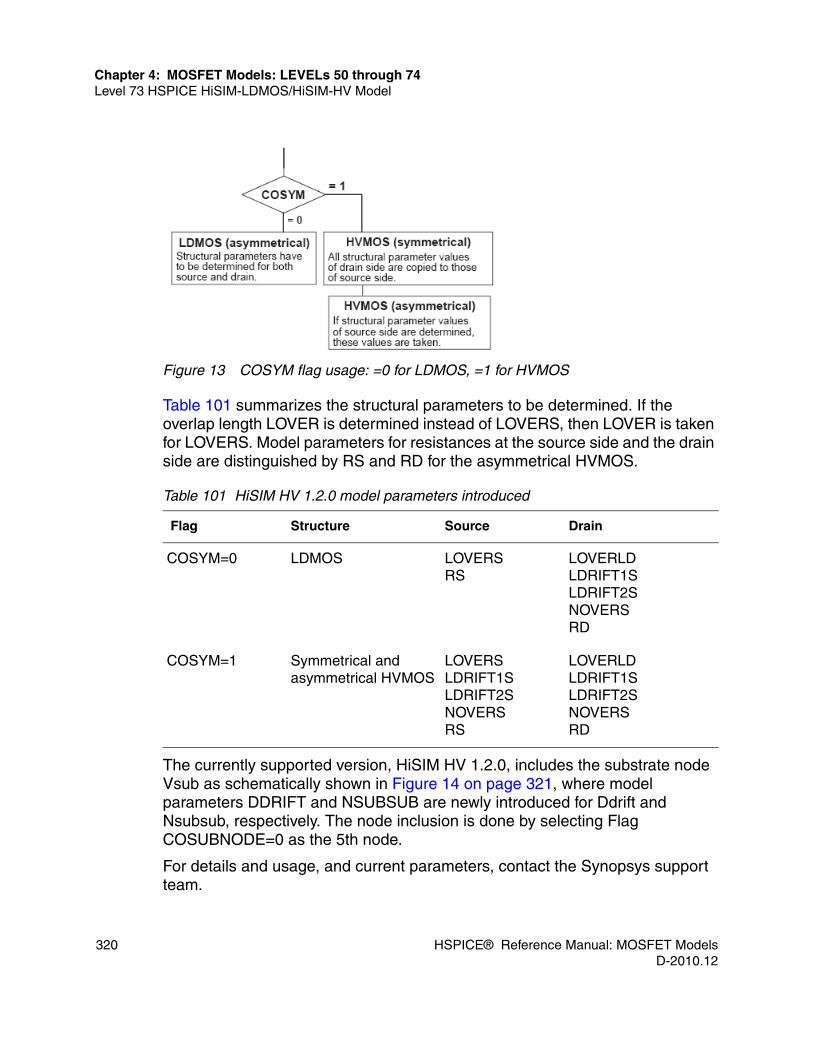
320 HSPICE® Reference Manual: MOSFET ModelsD-2010.12
Chapter 4: MOSFET Models: LEVELs 50 through 74Level 73 HSPICE HiSIM-LDMOS/HiSIM-HV Model
Figure 13 COSYM flag usage: =0 for LDMOS, =1 for HVMOS
Table 101 summarizes the structural parameters to be determined. If the overlap length LOVER is determined instead of LOVERS, then LOVER is taken for LOVERS. Model parameters for resistances at the source side and the drain side are distinguished by RS and RD for the asymmetrical HVMOS.
The currently supported version, HiSIM HV 1.2.0, includes the substrate node Vsub as schematically shown in Figure 14 on page 321, where model parameters DDRIFT and NSUBSUB are newly introduced for Ddrift and Nsubsub, respectively. The node inclusion is done by selecting Flag COSUBNODE=0 as the 5th node.
For details and usage, and current parameters, contact the Synopsys support team.
Table 101 HiSIM HV 1.2.0 model parameters introduced
Flag Structure Source Drain
COSYM=0 LDMOS LOVERSRS
LOVERLDLDRIFT1SLDRIFT2SNOVERSRD
COSYM=1 Symmetrical and asymmetrical HVMOS
LOVERSLDRIFT1SLDRIFT2SNOVERSRS
LOVERLDLDRIFT1SLDRIFT2SNOVERSRD

HSPICE® Reference Manual: MOSFET Models 321D-2010.12
Chapter 4: MOSFET Models: LEVELs 50 through 74Level 73 HSPICE HiSIM-LDMOS/HiSIM-HV Model
Figure 14 Schematic of a LDMOS with the substrate node Vsub,s
Note: HiSIM-LDMOS source code, and all copyrights, trade secrets or other intellectual property rights in and to the source code in its entirety, is owned by Hiroshima University and STARC.
This section discusses the following topics■ General Syntax for the HiSIM-LDMOS-1.2.0 Level 73 Model■ Template Output for Parameters in HiSIM-HVMOS v.1.2.0 and Higher■ Previous Versions of the HiSIM LDMOS-HVMOS Model
General Syntax for the HiSIM-LDMOS-1.2.0 Level 73 ModelThe following lists and describes the HiSIM-LDMOS/HVMOS-1.2.0 Level 73 general parameters.
Mxxx nd ng ns [nb] mname [L=val][W=val [M=val]+ [AD=val] [AS=val] [PD=val] [PS=val]+ [NRS=val] [NRD=val] [XGW=val] [XGL=val]+ [NF=val] [NGCON=val] [RBPB=val] [RBPD=val]+ [RBPS=val] [SA=val] [SB=val] [SD=val] [DTEMP=val]+ [NSUBCDFM=val] [SUBLD1=val] [SUBLD2=val]+ [LDRIFT1=val][LDRIFT2=val] [LDSRIFT1S=val] [LDRIFT2S=val]+ [LOVER=val] [LOVERLD=val] [LOVERS=val]+ [COSELFHEAT=val] [CONSUBNODE=val]

322 HSPICE® Reference Manual: MOSFET ModelsD-2010.12
Chapter 4: MOSFET Models: LEVELs 50 through 74Level 73 HSPICE HiSIM-LDMOS/HiSIM-HV Model
Notes for Mxxx Card■ nd, ng, ns, nb: drain, gate, source, and bulk node, respectively■ nsub: substrate node■ nth: thermal node■ The square brackets “[ ]" indicate optional content which may be omitted.■ If 5 nodes are specified and COSUBNODE=0, the 5th node is nth.
• If 5 nodes are specified and COSUBNODE=1, the 5th node is nsub.
• If 6 nodes are specified, the 5th node is nsub and the 6th nod is nth.■ COSUBNODE is a new instance parameter and at the same time is
recognized as a model parameter for the specification and the recognition of the node order.
■ Originally COSELFHEAT was treated as a model parameter as other flags. It is additionally recognized as an instance parameter.
■ See Table 103 on page 325 for model options and descriptions.

HSPICE® Reference Manual: MOSFET Models 323D-2010.12
Chapter 4: MOSFET Models: LEVELs 50 through 74Level 73 HSPICE HiSIM-LDMOS/HiSIM-HV Model
General Model ParametersTable 102 HiSIM-LDMOS/HVMOS Level 73 Instance Parameters
Parameter Default Description
L 2.0 Gate length (Lgate)
W 5.0 Gate width (Wgate)
Diode
AD 0.0 Area of drain junction
AS 0.0 Area of source junction
PD 0.0 Perimeter of drain junction
PS 0.0 Perimeter of source junction
Source/Drain Resistance
NRS 1.0 Number of source squares
NRD 1.0 Number of drain squares
Gate Resistance
XGW 0.0 Distance from the gate contact to the channel edge
XGL 0.0 Offset of the gate length
NF 1.0 Number of gate fingers
M 1.0 Multiplication factor
NGCON 1.0 Number of gate contacts
Substrate Network
RBPB Model parameter value
Substrate Resistance Network
RBPD Model parameter value
Substrate Resistance Network
RBPS Model parameter value
Substrate Resistance Network
μm
μm

324 HSPICE® Reference Manual: MOSFET ModelsD-2010.12
Chapter 4: MOSFET Models: LEVELs 50 through 74Level 73 HSPICE HiSIM-LDMOS/HiSIM-HV Model
RBDB Obsolete
RBSB Obsolete
Lenth of Diffusion
SA 0.0 Length of diffusion between gate and STI
SB 0.0 Length of diffusion between gate and STI
SD 0.0 Length of diffusion between gate and gate
Temperature
DTEMP 0.0 Device temperature change
Design for Manufacturability
NSUBCDFM 0.0 Substrate impurity concentration
Substrate Current
SUBLD1 Model parameter value
Substrate current induced in Ldrift
SUBLD2 Model parameter value
Substrate current induced in Ldrift
Resistance
LDRIFT1 0.0 Length of lightly doped drift region
LDRIFT2 1.0 Length of heavily doped drift region
LDRIFT1S 0.0 Length of lightly doped drift region in source side
LDRIFT2S 1.0 Length of heavily doped drift region in source side
Table 102 HiSIM-LDMOS/HVMOS Level 73 Instance Parameters (Continued)
Parameter Default Description
μm
μm

HSPICE® Reference Manual: MOSFET Models 325D-2010.12
Chapter 4: MOSFET Models: LEVELs 50 through 74Level 73 HSPICE HiSIM-LDMOS/HiSIM-HV Model
Control Option Flags for LDMOS-HVMOS 1.2.0 ModelThe following control flags are operational for the LDMOS-HVMOS 1.2.0 model
Overlap
LOVER 0.0 Length of overlap region in source side for LDMOS
LOVERLD Model parameter value
Length of overlap region in drain side
LOVERS Model parameter value
Length of overlap region in source side for HVMOS
COSELFHEAT Model parameter value
Flag to switch on the self-heating effect
COSUBNODE Model parameter value
Flag for selection of the 5th node
Table 103 HiSIM LDMOS-HVMOS Level 73 Control Options
Description Flag
1 Selects asymmetrical (LDMOS) or HVMOS structure
■ COSYM = 0: asymmetrical LDMOS (default)■ COSYM = 1: symmetrical and asymmetrical
HVMOS
2 Include contact resistances Rs and Rd ■ CORSRD= 0: no ■ CORSRD = 1 & : yes, as internal
resistance nodes■ CORSD=2 & : yes, analytical
description■ CORSD=3 & : yes, analytical
description (default)■ CORSRD = -1 & : yes, as external
resistance nodes
3 Adds overlap charges/capacitances to intrinsic ones
■ COADOV = 0: no■ COADOV = 1: yes (default)
Table 102 HiSIM-LDMOS/HVMOS Level 73 Instance Parameters (Continued)
Parameter Default Description
RS RD 0≠⁄
RS RD 0≠⁄
RS RD 0≠⁄
RS RD 0≠⁄

326 HSPICE® Reference Manual: MOSFET ModelsD-2010.12
Chapter 4: MOSFET Models: LEVELs 50 through 74Level 73 HSPICE HiSIM-LDMOS/HiSIM-HV Model
4 Selects bias-dependent overlap capacitance model at drain side
■ COOVLP = 0: constant overlap capacitance■ COOVLP = 1: yes (default) including constant
values as option
5 Selects bias-dependent overlap capacitance model at source side
■ COOVLPS = 0: constant overlap capacitance■ COOVLP = 1: yes (default) including constant
values as option
6 Considers self-heating effect ■ COSELFHEAT = 0: no (default)■ COSELFHEAT = 1: yes
7 Calculates substrate current Isub ■ COISUB = 0: no (default)■ COISUB = 1: yes
8 Calculates gate current Igate ■ COIIGS = 0: no (default)■ COIIGS = 1: yes
9 Calculates GIDL current IGIDL ■ COGIDL = 0: no (default)■ COGIDL = 1: yes
10 Calculates STI leakage current Ids,STI ■ COISTI = 0: no (default)■ COISTI = 1: yes
11 Invokes non-quasi-static ■ CONQS = 0: no (default)■ CONQS = 1: yes
12 Includes gate-contact resistance ■ CORG = 0: no (default)■ CORG = 1: yes
13 Invokes substrate resistance network ■ CORBNET = 0: no (default)■ CORBNET = 1: yes
14 Calculates 1/f noise ■ COFLICK = 0: no (default)■ COFLICK = 1: yes
15 Calculates thermal noise ■ COTHRML = 0: no (default)■ COTHRML = 1: yes
16 Calculates induced-gate and cross-correlation noise
■ COIGN = 0 k COTHRML = 0: no (default)■ COIGN = 1 & COTHRML = 1: yes
17 Uses previous _S for the iteration ■ COPPRV = 0: no■ COPPRV = 1: yes (default)
Table 103 HiSIM LDMOS-HVMOS Level 73 Control Options
Description Flag

HSPICE® Reference Manual: MOSFET Models 327D-2010.12
Chapter 4: MOSFET Models: LEVELs 50 through 74Level 73 HSPICE HiSIM-LDMOS/HiSIM-HV Model
For full information regarding the HiSIM 1.2.0 version of this model, see HiSIM_HV 1.1.0 User's Manual, available through Hiroshima University and STARC.
Template Output for Parameters in HiSIM-HVMOS v.1.2.0 and HigherHSPICE supports parameter template output beginning with HiSIM-HV1.2.0 model (version=1.20, level=73).
18 Considers parameter variations for DFM support
■ CODFM = 0: no (default)■ CODFM = 1: yes
19 Uses previous Ids is used for calculating source/drain resistance effect ( ): This flag is deactivated.
■ COIPRV = 0: no■ COIPRV = 1: yes (default)
20 Selects temperature dependence of models
Rd0,temp Rdvd,temp Vmax Ninvd
■ COTEMP=0 T T0 T0 T0 (default and backward compatible)
■ COTEMP=1 T0 T0 T0 T0■ COTEMP=2 T T T T■ COTEMP=3 T T T0 T0where T includes the temperature increase by the self-heating effect and T0 omits it.
21 Selects the 5th node ■ COSUBNODE = 0: the 5th node is the thermal node.
■ COSUBNODE = 1: the 5th node is the Vsub node.
22 Selects the Ldrift ■ COLDRIFT = 0: Ldrift includes LOVER (default & backward compatible)
■ COLDRIFT = 1: without LOVER.
Table 104 Output Templates for HiSIM LDMOD/HDMOS Model -1.2.0
Name Alias Description
L LX291 Channel Length (L)
Table 103 HiSIM LDMOS-HVMOS Level 73 Control Options
Description Flag
RSand orRD 0≠

328 HSPICE® Reference Manual: MOSFET ModelsD-2010.12
Chapter 4: MOSFET Models: LEVELs 50 through 74Level 73 HSPICE HiSIM-LDMOS/HiSIM-HV Model
W LX292 Channel Width (W)
AD LX293 Area of the drain diode (AD)
AS LX294 Area of the source diode (AS)
ICVDS LX295 Initial condition for the drain-source voltage (VDS)
ICVGS LX296 Initial condition for the gate-source voltage (VGS)
ICVBS LX297 Initial condition for the bulk-source voltage (VBS)
PD LX298 Drain diode periphery (PD)
PS LX299 Source diode periphery (PS)
RSS LX301 Source resistance (squares) (RSS)
WEFF LX302 Effective channel width
LEFF LX303 Effective channel length
CAPFG LX304 Fringing capacitance
VTH LX305 Threshold voltage (bias dependent)
VDSAT LX306 Saturation voltage (VDSAT)
GDEFF LX307 Effective drain conductance (1/RDeff)
GSEFF LX308 Effective source conductance (1/RSeff)
VDBEFF LX309 Effective drain bulk voltage.
BETAEFF LX310 BETA effective
GAMMAEFF LX311 GAMMA effective
VFBEFF LX312 VFB effective
COVLGS LX313 Gate-source overlap and fringing capacitances
Table 104 Output Templates for HiSIM LDMOD/HDMOS Model -1.2.0
Name Alias Description

HSPICE® Reference Manual: MOSFET Models 329D-2010.12
Chapter 4: MOSFET Models: LEVELs 50 through 74Level 73 HSPICE HiSIM-LDMOS/HiSIM-HV Model
COVLGD LX314 Gate-drain overlap and fringing capacitances
COVLGB LX315 Gate-bulk overlap capacitances
VBD LX316 Bulk-drain voltage
VBS LX317 Bulk-source voltage (VBS)
VGS LX318 Gate-source voltage (VGS)
VDS LX319 Drain-source voltage (VDS)
CDO LX320 Channel current (IDS)
CBSO LX321 DC source-bulk diode current (CBSO)
CBDO LX322 DC drain-bulk diode current (CBDO)
GMO LX323 DC MOSFET gate transconductance (GMO)
GDSO LX324 DC drain-source conductance (GDSO)
GMBSO LX325 DC substrate transconductance (GMBSO)
GBDO LX326 Conductance of the drain diode (GBDO)
GBSO LX327 Conductance of the source diode (GBSO)
QB LX328 Total bulk (body) charge (QB)—Meyer and Charge Conservation
CQB LX329 Bulk (body) charge current (CQB)—Meyer and Charge Conservation
QG LX330 Total Gate charge (QG)—Meyer and Charge Conservation
CQG LX331 Gate charge current (CQG)—Meyer and Charge Conservation
QD LX332 Channel charge (QD)
CQD LX333 Channel charge current (CQD)
CGGBO LX334 Intrinsic gate capacitance
Table 104 Output Templates for HiSIM LDMOD/HDMOS Model -1.2.0
Name Alias Description

330 HSPICE® Reference Manual: MOSFET ModelsD-2010.12
Chapter 4: MOSFET Models: LEVELs 50 through 74Level 73 HSPICE HiSIM-LDMOS/HiSIM-HV Model
CGDBO LX335 Intrinsic gate-to-drain capacitance
CGSBO LX336 Intrinsic gate-to-source capacitance
CBGBO LX337 Intrinsic bulk-to-gate capacitance
CBDBO LX338 Intrinsic bulk-to-drain capacitance
CBSBO LX339 CBSBO = -dQb/dVs
QBD LX340 Drain-bulk charge (QBD)
QBS LX341 Source-bulk charge (QBS)
CAP_BS LX342 Bias dependent bulk-source capacitance
CAP_BD LX343 Bias dependent bulk-drain capacitance
CDGBO LX344 Intrinsic drain-to-gate capacitance
CDDBO LX345 Intrinsic drain capacitance
CDSBO LX346 CDSBO = -dQd/dVs, Drain-to-source capacitance
SFT LX347 Value of the temperature node
weffcv LX348 Effective channel width for CV
leffcv LX349 Effective channel length for CV
igso LX350 Gate-to-Source Current
igdo LX351 Gate-to-Drain Current
igbo LX352 Gate-to-Substrate Current
igcso LX353 Source Partition of Igc
igcdo LX354 Drain Partition of Igc
iimi LX355 Impact ionization current
Table 104 Output Templates for HiSIM LDMOD/HDMOS Model -1.2.0
Name Alias Description

HSPICE® Reference Manual: MOSFET Models 331D-2010.12
Chapter 4: MOSFET Models: LEVELs 50 through 74Level 73 HSPICE HiSIM-LDMOS/HiSIM-HV Model
igidlo LX356 Gate-induced drain leakage current
igislo LX357 Gate-induced source leakage current
igdt LX358 Gate Dielectric Tunneling Current (Ig = Igs + Igd + Igcs + Igcd + Igb)
vgse LX359 Effective Gate-to-Source Voltage
rdv LX360 Asymmetric and Bias-Dependent Source Resistance
rsv LX361 Asymmetric and Bias-Dependent Drain Resistance
cap_bsz LX362 Zero voltage bias bulk-source capacitance
cap_bdz LX363 Zero voltage bias bulk-drain capacitance
CGGBM LX364 Total gate capacitance (including intrinsic), and overlap and fringing components
CGDBM LX365 Total gate-to-drain capacitance (including intrinsic), and overlap and fringing components
CGSBM LX366 Total gate-to-source capacitance (including intrinsic), and overlap and fringing components
CDDBM LX367 Total drain capacitance (including intrinsic), overlap and fringing components, and junction capacitance
CDSBM LX368 Total drain-to-source capacitance
CDGBM LX369 Total drain-to-gate capacitance (including intrinsic), and overlap and fringing components
CBGBM LX370 Total bulk-to-gate (floating body-to-gate) capacitance, including intrinsic and overlap components
CBDBM LX371 Total bulk-to-drain capacitance (including intrinsic) and junction capacitance
CBSBM LX372 Total bulk-to-source capacitance (including intrinsic), and junction capacitance
Table 104 Output Templates for HiSIM LDMOD/HDMOS Model -1.2.0
Name Alias Description

332 HSPICE® Reference Manual: MOSFET ModelsD-2010.12
Chapter 4: MOSFET Models: LEVELs 50 through 74Level 73 HSPICE HiSIM-LDMOS/HiSIM-HV Model
Previous Versions of the HiSIM LDMOS-HVMOS ModelThe following sections discuss updates to the model as they occurred:■ HISIM-LDMOS-100 Updates■ Extension to LDMOS and HVMOS■ HiSIM-HV Version 1.0.1 and 1.0.2
HISIM-LDMOS-100 UpdatesThe following changes were made in the HiSIM-LDMOS 100 model as reported in the SC1 through SC3 release notes provided by Hiroshima University/STARC.■ SC1:
• Self-heating effect Temperature node is handled as an internal node.
• The model parameter RD26 was deleted, and the smoothing parameter was fixed to a constant value.
• Qover Overlap Capacitance: The model description of Qover was changed from external bias to internal bias.
Ueff LX373 Effective mobility at the specified analysis temperature
VGB LX374 Gate to bulk voltage
VDG LX375 Drain to gate voltage
mult LX376 Prints value of multiplier (M) for a specified MOSFET
sa LX377 sa for STI or LOD-induced mechanical stress-effects
sb LX378 sb for STI or LOD-induced mechanical stress-effects
sd LX379 sd for STI or LOD-induced mechanical stress-effects
hsmhv_nf LX380 nf for STI or LOD-induced mechanical stress-effects
Table 104 Output Templates for HiSIM LDMOD/HDMOS Model -1.2.0
Name Alias Description

HSPICE® Reference Manual: MOSFET Models 333D-2010.12
Chapter 4: MOSFET Models: LEVELs 50 through 74Level 73 HSPICE HiSIM-LDMOS/HiSIM-HV Model
• The charge-partitioning scheme with model parameters QOVRAT1 and QOVRAT2 was deactivated.
• The new model parameter RD26 was introduced to fit transition characteristics at depletion and/or inversion.
■ SC2:
• The self-heating effect (COSELFHEAT=1) was stabilized for HSPICE. The temperature node can be treated either as and external or internal node.
• The NF dependability in the drift resistance model was removed for to improve accuracy.
■ SC3:
• The self-heating effect became applicable for AC analysis
• Introduction of drift-length (LDRIFT) dependence of the drift resistance.
• Introduction of model parameters RDTEMP1 and RDTEMP2 for temperature dependent drift resistance.
Extension to LDMOS and HVMOS To facilitate the structural definition, the COSYM flag was introduced with HiSIM-HV1.0.0. COSYM=0 refers to the asymmetrical LDMOS, and all drain-side and source-side parameters of the drain side are copied to the source side. COSYM=1 refers to symmetrical HVMOS, and all parameters have to be determined independently. HiSIM-LDMOS/HV considers the length of the drift region Ldrift, the overlap length Lover, and the impurity concentration of the drift region Nover explicitly. In the HVMOS case, the parameter values for the drain side have to be determined, and are copied to the source side automatically. If parameters are not determined, default values are taken.
HiSIM-HV Version 1.0.1 and 1.0.2HSPICE supports HiSIM-HV 1.0.1, version 1.01 and 1.0.2, version 1.02. To address the need for accurate modeling of high-voltage MOSFETs, Hiroshima University and STARC developed the HISIM-HVMOS model as an extension to the IGFET model. The HV model focuses on symmetrical structure while the HiSIM-LDMOS model is used for asymmetrical structures. According to the HiSIM_HV User Guide: the most important advantage of the surface-potential-based modeling is the unified description of device characteristics for all bias conditions. The physical reliability of the drift-diffusion theory has been proved

334 HSPICE® Reference Manual: MOSFET ModelsD-2010.12
Chapter 4: MOSFET Models: LEVELs 50 through 74Level 73 HSPICE HiSIM-LDMOS/HiSIM-HV Model
by 2-D device simulations with channel lengths even down to below 0:1 m. To obtain analytical solutions for describing device performances, the charge sheet approximation of the inversion layer with zero thickness has been introduced. Together with the gradual-channel approximation all device characteristics are then described analytically by the channel-surface potentials at the source side (S0) and at the drain side (SL) (see Figure 15 on page 334).
Figure 15 Schematic of the surface potential distribution in the channel
These surface potentials are functions of applied voltages on the four terminals: the gate voltage Vg, the drain voltage Vd, the bulk voltage Vb and the reference potential of the source Vs. The resistance in the contact region causing potential drops also affects the surface potential values. Since the surface potentials are implicit functions of the applied voltages, model-internal iteration procedures are introduced only for calculating , and is calculated in addition to the global iteration of the circuit simulator.
The potential is calculated with , , and together with a fitting
parameter.
The most important features of LDMOS/HVMOS devices, different from the conventional MOSFET, originate from the drift region introduced to achieve the sustainability of high voltages. By varying the length as well as the dopant concentration of the drift region, various devices with various operating bias conditions are realized. In many cases, the drift region acts as the resistance for the current flow and also induces additional charge, which causes the
μ
φS0 φSL
φs ΔL( ) φS0 φSL Vds

HSPICE® Reference Manual: MOSFET Models 335D-2010.12
Chapter 4: MOSFET Models: LEVELs 50 through 74Level 74 MOS Model 20 Model
especially unique features of the LDMOS capacitances. Thus, accurate modeling of the drift region is the main task of HiSIM-LDMOS/HV.
For the LDMOS/HVMOS devices the iterative solution is only one possible to model the specific features of this device accurately, because the resistance effect in the drift region is dependent on the bias condition as well as the detailed geometrical LDMOS/HVMOS structure. The basic modeling method is taken over from the HiSIM2 model for advanced MOSFETs, and additional equations for capturing the drift-region effects are included. Since the overlap length is relatively long for LDMOS/HVMOS, accurate surface potential calculation for the overlap region as a function of applied voltages is also necessary for accurate prediction of the high-voltage MOS capacitances.
Level 74 MOS Model 20 Model
MOS Model 20 (MM20) is a compact MOSFET model developed by NXP, intended for analog circuit simulation in high-voltage MOS technologies. MOS Model 20 describes the electrical behavior of the region under the thin gate oxide of a high-voltage MOS device, similar to a Lateral Double-diffused MOS (LDMOS) device or an extended-drain MOSFET. It combines the MOSFET-operation of the channel region with that of the drift region under the thin gate oxide in a high-voltage MOS device. As such, MOS Model 20 is aimed as a successor of the combination of MOS Model 9 (MM9) for the channel region in series with MOS Model 31 (MM31) for the drift region under the thin gate oxide, in macro models of various high-voltage MOS devices. MOS Model 20 has especially been developed to improve the convergence behavior during simulation, by having the voltage at the transition from the channel region to the drift region calculated inside the model itself.
Please check following URL from NXP for original MOS Model 20 release and documentation.
http://www.nxp.com/models/hv_models/model20/
The following sections discuss these topics:■ General Syntax for MOS Model 20 Model■ MOS Model 20 Instance and Model Parameter Lists■ Addition to HSPICE MOS Model 20 Implementation

336 HSPICE® Reference Manual: MOSFET ModelsD-2010.12
Chapter 4: MOSFET Models: LEVELs 50 through 74Level 74 MOS Model 20 Model
General Syntax for MOS Model 20 ModelMxxxx drain gate source bulk mname W=val Wd=val …
MOS Model 20 Instance and Model Parameter Lists
MM 20 Geometrical Model Parameters
Table 105 Instance Parameters for MOS Model 20
Name Unit Default Description
W m 2E-5 Drawn width of the channel region
WD m 2E-5 Drawn width of the drift region
MULT 1 Number of devices in parallel
Table 106 Geometrical Model Parameters
Name Unit Default Description
LEVEL 74 HSPICE model level as 74 for MOS Model 20
VERSION 2002.2 VERSION 2002.2 is the default version number to define NXP model level 2002
GEOMOD 1 GEOMOD is used as a switch between geometrical model and electrical model, 0 for geometrical model and 1 for electrical model
WVAR m 0 Width offset of the channel region
WDVAR m 0 Width offset of the drift region
TREF deg.C 25 Reference temperature
VFB V -1 Flatband voltage of the channel region, at reference temperature
STVFB V/K 0 Temperature scaling coefficient for VFB

HSPICE® Reference Manual: MOSFET Models 337D-2010.12
Chapter 4: MOSFET Models: LEVELs 50 through 74Level 74 MOS Model 20 Model
VFBD V -0.1 Flatband voltage of the drift region, at reference temperature
STVFBD V/K 0 Temperature scaling coefficient for the flatband voltage of the drift region
KOR V(1/2) 1.6 Body factor of the channel region of an infinitely wide transistor
SWKO 0 Width scaling coefficient for KO
KODR V(1/2) 1 Body factor of the drift region of an infinitely wide transistor
SWKOD 0 Width scaling coefficient for the body factor of the drift region
PHIB V 0.86 Surface potential at the onset of strong inversion in the channel region, at reference temperature
STPHIB V/K -0.0012 Temperature scaling coefficient for PHIB
PHIBD V 0.78 Surface pot anti al at the onset of strong inversion in the drift region, at reference temperature
STPHIBD V/K -0.0012 Temperature scaling coefficient for PHIBD
BETW A/V2 7.00E-05 Gain factor of a channel region of 1 um wide, at reference temperature
ETABET 1.6 Temperature scaling exponent for BET
BETACCW A/V2 7.00E-05 Gain factor of drift region of 1 um wide, at reference temperature
ETABETACC 1.5 Temperature scaling exponent for BETACC
RDW Ohm 4000 On-resistance of a drift region of 1 um wide, at reference temperature
ETARD 1.5 Temperature scaling exponent for RD
Table 106 Geometrical Model Parameters (Continued)
Name Unit Default Description

338 HSPICE® Reference Manual: MOSFET ModelsD-2010.12
Chapter 4: MOSFET Models: LEVELs 50 through 74Level 74 MOS Model 20 Model
LAMD 0.2 Quotient of the depletion layer thickness to the effective thickness of the drift region at VSB = 0 V
THE1R V-1 0.09 Mobility reduction coefficient of infinitely wide transistor, due to vertical strong-inversion field in a channel region
SWTHE1 0 Width scaling coefficient for THE1
THE1ACC V-1 0.02 Mobility reduction coefficient in the drift region due to the vertical electrical field caused by accumulation
THE2R V(-1/2) 0.03 Mobility reduction coefficient for VSB > 0 of an infinitely wide transistor, due to vertical depletion field in channel region
SWTHE2 0 Width scaling coefficient for THE2
THE3R V-1 0.4 Mobility reduction coefficient in a channel region of an infinitely wide transistor due to velocity saturation
ETATHE3 1 Temperature scaling exponent for THE3
SWTHE3 0 Width scaling coefficient for THE3
MEXP 2 Smoothing factor for transition from linear to saturation regime
THE3DR V-1 0 Mobility reduction coefficient in a channel region of an infinitely wide transistor due to velocity saturation
ETATHE3D 1 Temperature scaling exponent for THE3D
SWTHE3D 0 Width scaling coefficient for THE3D
MEXPD 2 Smoothing factor for transition from linear to quasi-saturation regime
ALP 0.002 Factor for channel length modulation
VP V 0.05 Characteristic voltage of channel length modulation
SDIBL V(-1/2) 0.001 Factor for drain-induced barrier lowering
Table 106 Geometrical Model Parameters (Continued)
Name Unit Default Description

HSPICE® Reference Manual: MOSFET Models 339D-2010.12
Chapter 4: MOSFET Models: LEVELs 50 through 74Level 74 MOS Model 20 Model
MSDIBL 3 Exponent for the drain-induced barrier lowering dependence on the backgate bias
MO V 0 Parameter for the (short-channel) sub-threshold slope
SSF V(-1/2) 1E-12 Factor for static feedback
A1CHR 15 Factor of channel weak avalanche current, at reference temperature
STA1CH K-1 0 Temperature scaling coefficient for A1CH
SWA1CH 0 Width scaling coefficient for A1CH
A2CH V 73 Exponent of weak avalanche current, related to channel
A3CH 0.8 Factor of the internal drain-source voltage, above which channel weak avalanche occurs
A1DRR 15 Factor of drift weak avalanche current, at reference temperature
STA1DR K-1 0 Temperature scaling coefficient for A1DR
SWA1DR 0 Width scaling coefficient for A1DR
A2DR V 73 Exponent of weak avalanche current, related to drift
A3DR 0.8 Factor of the internal drain-source voltage, above which drift weak avalanche occurs
COXW F 7.5E-16 Oxide capacitance for an intrinsic channel region of 1 um wide
COXDW F 7.5E-16 Oxide capacitance for an intrinsic drift region of 1 um wide
CGDOW F 0 Gate-to-drain overlap capacitance for a drift region of 1 um wide
CGSOW F 0 Gate-to-source overlap capacitance for a drift region of 1 um wide
Table 106 Geometrical Model Parameters (Continued)
Name Unit Default Description

340 HSPICE® Reference Manual: MOSFET ModelsD-2010.12
Chapter 4: MOSFET Models: LEVELs 50 through 74Level 74 MOS Model 20 Model
MM20 Electrical Model Parameters
NT J 1.645E-20 Coefficient of thermal noise, at reference temperature
NFAW 1.4E+25 First coefficient of flicker noise for a channel region of 1 um wide
NFBW 2.00E+08 Second coefficient of flicker noise for a channel region of 1 um wide
NFCW V-1 0 Third coefficient of flicker noise for a channel region of 1 um wide
TOX m 3.80E-08 Thickness of the oxide above the channel region
DTA K 0 Temperature offset to the ambient temperature
SHMOD 0 SHMOD is used as a switch of self-heating effect, 0 for off and 1 for on
RTH K/W 300 Thermal resistance
CTH J/K 3.00E-09 Thermal capacitance
ATH 0 Temperature coefficient of the thermal resistance
JUNCAPMOD 0 JUNCAPMOD as a switch of juncap200.2 model effective, 0 for off and 1 for on
Table 107 Electrical Model Parameters
Name Unit Default Description
VERSION 2002.2 VERSION 2002.2 is the default version number to define NXP model level 2002
GEOMOD 1 GEOMOD is used as a switch between geometrical model and electrical model, 0 for geometrical model and 1 for electrical model
TYPE 1 TYPE=1 NMOS;TYPE=-1 PMOS
Table 106 Geometrical Model Parameters (Continued)
Name Unit Default Description
V1m– 4–
V1m– 2–

HSPICE® Reference Manual: MOSFET Models 341D-2010.12
Chapter 4: MOSFET Models: LEVELs 50 through 74Level 74 MOS Model 20 Model
TREF deg.C 25 Reference temperature
VFB V -1 Flatband voltage of the channel region, at reference temperature
STVFB V/K 0 Temperature scaling coefficient for VFB
VFBD V -0.1 Flatband voltage of the drift region, at reference temperature
STVFBD V/K 0 Temperature scaling coefficient for the flatband voltage of the drift region
KO V(1/2) 1.6 Body factor of the channel region
KOD V(1/2) 1 Body factor of the drift region
PHIB V 0.86 Surface potential at the onset of strong inversion in the channel region, at reference temperature
STPHIB V/K -0.0012 Temperature scaling coefficient for PHIB
PHIBD V 0.78 Surface potential at the onset of strong inversion in the drift region, at reference temperature
STPHIBD V/K -0.0012 Temperature scaling coefficient for PHIBD
BET A/V2 7.00E-05 Gain factor of a channel region, at reference temperature
ETABET 1.6 Temperature scaling exponent for BET
BETACC A/V2 7.00E-05 Gain factor of drift region of 1 um wide, at reference temperature
ETABETACC 1.5 Temperature scaling exponent for BETACC
RD Ohm 200 On-resistance of a drift region, at reference temperature
ETARD 1.5 Temperature scaling exponent for RD
Table 107 Electrical Model Parameters (Continued)
Name Unit Default Description
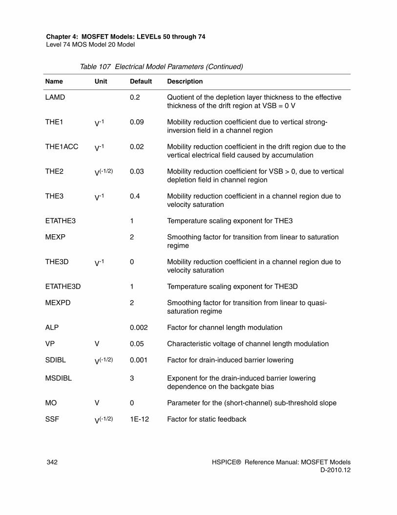
342 HSPICE® Reference Manual: MOSFET ModelsD-2010.12
Chapter 4: MOSFET Models: LEVELs 50 through 74Level 74 MOS Model 20 Model
LAMD 0.2 Quotient of the depletion layer thickness to the effective thickness of the drift region at VSB = 0 V
THE1 V-1 0.09 Mobility reduction coefficient due to vertical strong-inversion field in a channel region
THE1ACC V-1 0.02 Mobility reduction coefficient in the drift region due to the vertical electrical field caused by accumulation
THE2 V(-1/2) 0.03 Mobility reduction coefficient for VSB > 0, due to vertical depletion field in channel region
THE3 V-1 0.4 Mobility reduction coefficient in a channel region due to velocity saturation
ETATHE3 1 Temperature scaling exponent for THE3
MEXP 2 Smoothing factor for transition from linear to saturation regime
THE3D V-1 0 Mobility reduction coefficient in a channel region due to velocity saturation
ETATHE3D 1 Temperature scaling exponent for THE3D
MEXPD 2 Smoothing factor for transition from linear to quasi-saturation regime
ALP 0.002 Factor for channel length modulation
VP V 0.05 Characteristic voltage of channel length modulation
SDIBL V(-1/2) 0.001 Factor for drain-induced barrier lowering
MSDIBL 3 Exponent for the drain-induced barrier lowering dependence on the backgate bias
MO V 0 Parameter for the (short-channel) sub-threshold slope
SSF V(-1/2) 1E-12 Factor for static feedback
Table 107 Electrical Model Parameters (Continued)
Name Unit Default Description

HSPICE® Reference Manual: MOSFET Models 343D-2010.12
Chapter 4: MOSFET Models: LEVELs 50 through 74Level 74 MOS Model 20 Model
A1CH 15 Factor of channel weak avalanche current, at reference temperature
STA1CH K-1 0 Temperature scaling coefficient for A1CH
A2CH V 73 Exponent of weak avalanche current, related to channel
A3CH 0.8 Factor of the internal drain-source voltage, above which channel weak avalanche occurs
A1DR 15 Factor of drift weak avalanche current, at reference temperature
STA1DR K-1 0 Temperature scaling coefficient for A1DR
A2DR V 73 Exponent of weak avalanche current, related to drift
A3DR 0.8 Factor of the internal drain-source voltage, above which drift weak avalanche occurs
COX F 15E-15 Oxide capacitance for an intrinsic channel region
COXD F 15E-15 Oxide capacitance for an intrinsic drift region
CGDO F 0 Gate-to-drain overlap capacitance for a drift region
CGSO F 0 Gate-to-source overlap capacitance for a drift region
NT J 1.645E-20 Coefficient of thermal noise, at reference temperature
NFA 7.0E+23 First coefficient of flicker noise for a channel region
NFB 1.0E+07 Second coefficient of flicker noise for a channel region
NFC V-1 0 Third coefficient of flicker noise for a channel region
TOX m 3.80E-08 Thickness of the oxide above the channel region
DTA K 0 Temperature offset to the ambient temperature
Table 107 Electrical Model Parameters (Continued)
Name Unit Default Description
V1m– 4–
V1– m 2–

344 HSPICE® Reference Manual: MOSFET ModelsD-2010.12
Chapter 4: MOSFET Models: LEVELs 50 through 74Level 74 MOS Model 20 Model
Addition to HSPICE MOS Model 20 ImplementationJuncap 200.2 is supported in HSPICE MOS Model 20 as an alternative to the MOSFET junction diode model. You can use model parameter, JUNCAPMOD=1, to invoke Juncap200.2.
SHMOD 0 SHMOD is used as a switch of self-heating effect, 0 for off and 1 for on
RTH K/W 300 Thermal resistance
CTH J/K 3.00E-09 Thermal capacitance
ATH 0 Temperature coefficient of the thermal resistance
JUNCAPMOD 0 JUNCAPMOD as a switch of juncap200.2 model effective, 0 for off and 1 for on
Table 107 Electrical Model Parameters (Continued)
Name Unit Default Description

HSPICE® Reference Manual: MOSFET Models 345D-2010.12
5
5MOSFET Models (BSIM): Levels 13 through 39
Lists and describes three of the earliest BSIM-type MOSFET models supported by HSPICE.
This chapter describes three of the earliest Berkeley Short Channel IGFET (BSIM) type MOSFET device models that HSPICE supports:■ LEVEL 13 BSIM Model■ LEVEL 28 Modified BSIM Model■ LEVEL 39 BSIM2 Model
These models are all based on models developed by the University of California at Berkeley. You can find documentation on BSIM3 and BSIM4 at this website:
http://www.eigroup.org/cmc/cmos/default.htm
For descriptions of the newest BSIM models that Synopsys supports, see Chapter 6, MOSFET Models (BSIM): Levels 47 through 72.
LEVEL 13 BSIM Model
Level 13 is based on the SPICE 2G.6 BSIM model, which models the device physics of small-geometry MOS transistors. To invoke the subthreshold region, set the N0 model parameter (low field weak inversion gate drive coefficient) to less than 200. Level 13 provides three MOSFET models:

346 HSPICE® Reference Manual: MOSFET ModelsD-2010.12
Chapter 5: MOSFET Models (BSIM): Levels 13 through 39LEVEL 13 BSIM Model
■ Wire (resistor) model, compatible with the SPICE BSIM interconnect model for polysilicon and metal layers. Simulates resistors and capacitors with interconnects.
■ Capacitor model. Simulates only capacitors with interconnects.■ Diffusion model, compatible with SPICE BSIM diffusion models.
To set Level 13 model parameters, either:■ Enter model parameters as numbers (as in SPICE), or■ Assign the model parameters.
If you convert from SPICE to the Synopsys models, use the S keyletter for SPICE BSIM, or M for the Synopsys model. (see IDS and VGS Curves for PMOS and NMOS on page 368).
BSIM Model Features■ Vertical field dependence of the carrier mobility■ Carrier velocity saturation■ Drain-induced barrier lowering■ Depletion charge sharing by source and drain■ Non-uniform doping profile for ion-implanted devices■ Channel length modulation■ Subthreshold conduction■ Geometric dependence of electrical parameters
LEVEL 13 Model ParametersMOSFET Level 13 uses the generic MOSFET model parameters described in Chapter 2, Common MOSFET Model Parameters. It also uses the parameters described in this section, which apply only to MOSFET Level 13.
Note: When you read parameter names, be careful about the difference in appearance between the upper case letter O, the lower case letter o, and the number zero (0).

HSPICE® Reference Manual: MOSFET Models 347D-2010.12
Chapter 5: MOSFET Models (BSIM): Levels 13 through 39LEVEL 13 BSIM Model
For reference purposes only, simulation obtains the following default values from a medium size n-channel MOSFET device.
To specify Level 13 parameters, use NMOS conventions, even for PMOS (for example, ETA0=0.02, not ETA0=-0.02).
Table 108 Transistor Parameters, MOSFET Level 13
Name (Alias) Units Default Description
LEVEL 1 MOSFET model level selector. 13 is the BSIM model
CGBOM, (CGBO) F/m 2.0e-10 Gate-to-bulk parasitic capacitance (F/m of length)
CGDOM, (CGDO) F/m 1.5e-9 Gate-to-drain parasitic capacitance (F/m of width)
CGSOM, (CGSO) F/m 1.5e-9 Gate-to-source parasitic capacitance (F/m of width)
DL0 μm 0.0 Difference between drawn poly and electrical
DW0 μm 0.0 Difference between drawn diffusion and electrical
DUM1 0.0 Dummy (not used)
DUM2 0.0 Dummy (not used)
ETA0 0.0 Linear vds threshold coefficient
LETA mm 0.0 Length sensitivity
WETA μm 0.0 Width sensitivity
K1 V1/2 0.5 Root-vsb threshold coefficient
LK1 V1/ 2⋅ μm 0.0 Length sensitivity
WK1 V1/ 2⋅ μm 0.0 Width sensitivity
K2 0.0 Linear vsb threshold coefficient

348 HSPICE® Reference Manual: MOSFET ModelsD-2010.12
Chapter 5: MOSFET Models (BSIM): Levels 13 through 39LEVEL 13 BSIM Model
LK2 μm 0.0 Length sensitivity
WK2 μm 0.0 Width sensitivity
MUS cm2/(V⋅ s) 600 High drain field mobility
LMS (LMUS) μm⋅ cm2/(V⋅ s) 0.0 Length sensitivity
WMS (WMUS) μm⋅ cm2/(V⋅ s) 0.0 Width sensitivity
MUZ cm2/(V⋅ s) 600 Low drain field first order mobility
LMUZ μm⋅ cm2/(V⋅ s) 0.0 Length sensitivity
WMUZ μm⋅ cm2/(V⋅ s) 0.0 Width sensitivity
N0 0.5 Low field weak inversion gate drive coefficient (a value of 200 for N0 disables the weak inversion calculation)
LN0 0.0 Length sensitivity
WN0 0.0 Width sensitivity
NB0 0.0 Vsb reduction to the low field weak inversion gate drive coefficient
LNB 0.0 Length sensitivity
WNB 0.0 Width sensitivity
ND0 0.0 Vds reduction to the low field weak inversion gate drive coefficient
LND 0.0 Length sensitivity
WND 0.0 Width sensitivity
Table 108 Transistor Parameters, MOSFET Level 13
Name (Alias) Units Default Description

HSPICE® Reference Manual: MOSFET Models 349D-2010.12
Chapter 5: MOSFET Models (BSIM): Levels 13 through 39LEVEL 13 BSIM Model
PHI0 V 0.7 Two times the Fermi potential
LPHI V⋅ μm 0.0 Length sensitivity
WPHI V⋅ μm 0.0 Width sensitivity
TREF ° C 25.0 Reference temperature of model (local override of TNOM)
TOXM, (TOX) μm, (m) 0.02 Gate oxide thickness (simulation interprets TOXM or TOX >1 as Angstroms)
U00 1/V 0.0 Gate field mobility reduction factor
LU0 μm/V 0.0 Length sensitivity
WU0 μm/V 0.0 Width sensitivity
U1 μm/V 0.0 Drain field mobility reduction factor
LU1 μm2/V 0.0 Length sensitivity
WU1 μm2/V 0.0 Width sensitivity
VDDM V 50 Critical voltage for the high-drain field mobility reduction
VFB0 (VFB) V -0.3 Flatband voltage
LVFB V⋅ μm 0.0 Length sensitivity
WVFB V⋅ μm 0.0 Width sensitivity
X2E 1/V 0.0 Vsb correction to the linear vds threshold coefficient
LX2E μm/V 0.0 Length sensitivity
Table 108 Transistor Parameters, MOSFET Level 13
Name (Alias) Units Default Description

350 HSPICE® Reference Manual: MOSFET ModelsD-2010.12
Chapter 5: MOSFET Models (BSIM): Levels 13 through 39LEVEL 13 BSIM Model
WX2E μm/V 0.0 Width sensitivity
X2M (X2MZ) cm2/(V2⋅ s) 0.0 Vsb correction to the low field first-order mobility
LX2M (LX2MZ) μm⋅ cm2/(V2⋅ s) 0.0 Length sensitivity
WX2M (WX2MZ) μm⋅ cm2/(V2⋅ s) 0.0 Width sensitivity
X2MS cm2/(V2⋅ s) 0.0 Vbs reduction to the high-drain field mobility
LX2MS μm⋅ cm2/(V2⋅ s) 0.0 Length sensitivity
WX2MS μm⋅ cm2/(V2⋅ s) 0.0 Width sensitivity
X2U0 1/V2 0.0 Vsb reduction to the GATE field mobility reduction factor
LX2U0 μm/V2 0.0 Length sensitivity
WX2U0 μm/V2 0.0 Width sensitivity
X2U1 μm/V2 0.0 Vsb reduction to the DRAIN field mobility reduction factor
LX2U1 μm2/V2 0.0 Length sensitivity
WX2U1 μm2/V2 0.0 Width sensitivity
X3E 1/V 0.0 Vds correction to the linear vds threshold coefficient
LX3E μm/V 0.0 Length sensitivity
WX3E μm/V 0.0 Width sensitivity
X3MS cm2/(V2⋅ s) 5.0 Vds reduction to the high-drain field mobility
Table 108 Transistor Parameters, MOSFET Level 13
Name (Alias) Units Default Description
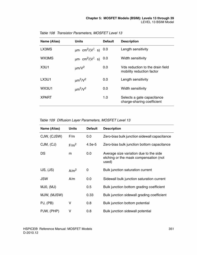
HSPICE® Reference Manual: MOSFET Models 351D-2010.12
Chapter 5: MOSFET Models (BSIM): Levels 13 through 39LEVEL 13 BSIM Model
LX3MS μm⋅ cm2/(V2⋅ s) 0.0 Length sensitivity
WX3MS μm⋅ cm2/(V2⋅ s) 0.0 Width sensitivity
X3U1 μm/V2 0.0 Vds reduction to the drain field mobility reduction factor
LX3U1 μm2/V2 0.0 Length sensitivity
WX3U1 μm2/V2 0.0 Width sensitivity
XPART 1.0 Selects a gate capacitance charge-sharing coefficient
Table 109 Diffusion Layer Parameters, MOSFET Level 13
Name (Alias) Units Default Description
CJW, (CJSW) F/m 0.0 Zero-bias bulk junction sidewall capacitance
CJM, (CJ) F/m2 4.5e-5 Zero-bias bulk junction bottom capacitance
DS m 0.0 Average size variation due to the side etching or the mask compensation (not used)
IJS, (JS) A/m2 0 Bulk junction saturation current
JSW A/m 0.0 Sidewall bulk junction saturation current
MJ0, (MJ) 0.5 Bulk junction bottom grading coefficient
MJW, (MJSW) 0.33 Bulk junction sidewall grading coefficient
PJ, (PB) V 0.8 Bulk junction bottom potential
PJW, (PHP) V 0.8 Bulk junction sidewall potential
Table 108 Transistor Parameters, MOSFET Level 13
Name (Alias) Units Default Description

352 HSPICE® Reference Manual: MOSFET ModelsD-2010.12
Chapter 5: MOSFET Models (BSIM): Levels 13 through 39LEVEL 13 BSIM Model
The wire model includes poly and metal layer process parameters.
Sensitivity Factors of Model ParametersTo denote the L (channel length) and W (channel width) sensitivity factors of a basic electrical parameter in a transistor, add L and W characters at the start of the name. For example, VFB0 sensitivity factors are LVFB and WVFB. If A0 is a basic parameter, then LA and WA are the corresponding L and W sensitivity factors of this parameter. Do not use the SCALM option to scale LA and WA.
The Level 13 MOSFET model uses the following equation to obtain this parameter value:
Specify LA and WA in units of microns times the units of A0.
RSHM, (RSH) ohm/sq 0.0 Sheet resistance/square
WDF m 0.0 Default width of the layer (not used)
Table 110 Temperature Parameters
Name (Alias) Units Default Description
BEX -1.5 Temperature exponent for the MUZ and MUS mobility parameters.
FEX 0.0 Temperature exponent for the U1 mobility reduction factor.
TCV V/°K 0.0 Flat-band voltage temperature coefficient.
TREF ° C 25 Temperature at which simulation extracts parameters. This parameter defaults to the TNOM option, which defaults to 25 ° C.
Table 109 Diffusion Layer Parameters, MOSFET Level 13
Name (Alias) Units Default Description
A A0 LA1
Leff---------- 1
LREFeff----------------------–⎝ ⎠
⎛ ⎞⋅ WA1
Weff------------ 1
WREFeff------------------------–⎝ ⎠
⎛ ⎞⋅+ +=

HSPICE® Reference Manual: MOSFET Models 353D-2010.12
Chapter 5: MOSFET Models (BSIM): Levels 13 through 39LEVEL 13 BSIM Model
The left side of the equation represents the effective model parameter value after you adjust the device size. All effective model parameters are in lower case and start with the z character, followed by the parameter name.
Example
,
,
,
,
.MODEL VERSION Changes to BSIM ModelsYou can use the VERSION parameter in the .MODEL statement to move Level 13 BSIM and Level 39 BSIM2 models between versions. Using the VERSION parameter in a Level 13 .MODEL statement results in the following changes to the BSIM model.
Model Version
Effect of VERSION on BSIM model
9007B Introduced the LEVEL 13 BSIM model: no changes
9007D Removed the K2 limit
92A Changed the TOX parameter default from 1000 A to 200 A
92B Added the K2LIM parameter, which specifies the K2 limit
93A Introduced the gds constraints
93A.02 Introduced the VERSION parameter
VFB0 0.350v–= LVFB 0.1vμ–=
WVFB 0.08v μ⋅= Leff 1 10 6–⋅ m 1μ= =
Weff 2 10 6–⋅ m 2μ= = LREFeff 2 10 6– m⋅ 2μ= =
WREFeff 1 10 5–⋅ m 10μ= =
zvfb VFB0 LVFB1
Leff---------- 1
LREFeff----------------------–⎝ ⎠
⎛ ⎞⋅ WVFB1
Weff------------ 1
WREFeff------------------------–⎝ ⎠
⎛ ⎞⋅+ +=
zvfb 0.35v– 0.1v– μ 11μ------ 1
2μ------–⎝ ⎠
⎛ ⎞⋅ ⋅ 0.08v μ 12μ------ 1
10μ---------–⎝ ⎠
⎛ ⎞⋅ ⋅+ +=
zvfb 0.35v– 0.05v– 0.032v+= zvfb 0.368v–=

354 HSPICE® Reference Manual: MOSFET ModelsD-2010.12
Chapter 5: MOSFET Models (BSIM): Levels 13 through 39LEVEL 13 BSIM Model
LEVEL 13 EquationsThis section lists the Level 13 model equations.
Effective Channel Length and WidthThe effective channel length and width for Level 13 depends on the specified model parameters.
If you specify DL0, then:
Otherwise, if you specify XL or LD:
If you specify DW0, then:
Otherwise, if you specify XW or WD, then:
IDS EquationsProcess-oriented model parameters model the device characteristics. Simulation maps these parameters into model parameters at a specific bias voltage. The ids equations are as follows:
95.1 Fixed the nonprinting TREF and incorrect GMBS problems
96.1 Changed the flatband voltage temperature adjustment
Model Version
Effect of VERSION on BSIM model
Leff Lscaled LMLT⋅ DL0 ⇒1e-6–=
LREFeff LREFscaled LMLT⋅ DL0 ⇒1e-6–=
Leff Lscaled LMLT⋅ XLscaled 2 ⇒LDscaled–+=
LREFeff LREFscaled LMLT⋅ XLscaled 2 ⇒LDscaled–+=
Weff Wscaled WMLT DW0 ⇒1e-6–⋅=
WREFeff WREFscaled WMLT DW0 ⇒1e-6–⋅=
Weff Wscaled WMLT XWscaled 2 ⇒WDscaled–+⋅=
WREFeff WREFscaled WMLT⋅ XWscaled 2 ⇒WDscaled–+=

HSPICE® Reference Manual: MOSFET Models 355D-2010.12
Chapter 5: MOSFET Models (BSIM): Levels 13 through 39LEVEL 13 BSIM Model
Cutoff Region, vgs £ vth
(see subthreshold current)
On Region, vgs >vthFor the vds<vdsat triode region:
For the vds>vdsat saturation region:
The following equations calculate values used in the preceding equation:
Simulation uses quadratic interpolation, through three data points to calculate the uo carrier mobility.
Simulation also calculates the sensitivity of uo to vds at vds=VDDM, which is zx3ms.
The following equation calculates the body factor:
The following equation calculates the g value used in the preceding equation:
The following equation calculates the arg term in the saturation region:
ids 0=
idsβ
1 xu1 vds⋅+---------------------------------- vgs vth–( ) vds⋅ body
2------------ ⇒vds2–⋅=
idsβ
2 body arg⋅ ⋅--------------------------------------- vgs vth–( )2⋅=
β ueff COXWeffLeff------------⋅ ⋅=
ueffuo
1 xu0 vgs vth–( )⋅+-----------------------------------------------------=
xu0 zu0 zx2u0 Þvsb–=
uovds 0=
MUZ zx2mz Þvsb–=
uovds VDDM=
zmus zx2ms Þvsb–=
body 1g zk1⋅
2 zphi vsb+( )1 2/⋅------------------------------------------------+=
g 11
1.744 0.8364 zphi vsb+( )⋅+--------------------------------------------------------------------------–=
arg12--- 1 vc 1 2 vc⋅+( )1 2/+ +[ ]⋅=

356 HSPICE® Reference Manual: MOSFET ModelsD-2010.12
Chapter 5: MOSFET Models (BSIM): Levels 13 through 39LEVEL 13 BSIM Model
The following equations calculate values used in the preceding equation:
, UPDATE=2
, UPDATE=0, 1
Threshold VoltageYou can express the threshold voltage as:
The following equations calculate values used in the preceding equation:
, UPDATE=0, 2
, UPDATE=1
Saturation Voltage (vdsat)The following equation calculates the saturation voltage in the BSIM Level 13 model:
ids Subthreshold CurrentSimulation calculates the isub subthreshold current if zn0 is less than 200:
The following equations calculate values used in the preceding equation:
,
vcxu1 vgs vth–( )⋅
body--------------------------------------------=
xu1 zu1 zx2u1 ⇒vsb– zx3u1 vds VDDM–( )⋅+=
xu1zu1 zx2u1 ⇒vsb– zx3u1 vds VDDM–( )⋅+
Leff----------------------------------------------------------------------------------------------------------------=
vth zvfb zphi gamma zphi vsb+( )1 2/⋅ xeta ⇒vds–+ +=
gamma zk1 zk2 ⇒zphi vsb+( )1 2/–=
xeta zeta zx2e ⇒vsb– zx3e vds VDDM–( )⋅+=
xeta zeta zx2e zphi vsb+( )⋅ zx3e vds VDDM–( )⋅+ +=
vdsatvgs vth–
body arg1 2/⋅------------------------------------=
isubIlim Iexp⋅Ilim Iexp+-----------------------------=
Iexp βo vt2 e1.8 evgs vth–xn vt⋅
----------------------1 e
vdsvt
--------––⎝ ⎠
⎛ ⎞⋅ ⋅ ⋅ ⋅=
Ilim 4.5 βo vt2⋅ ⋅= βo uo COXWeffLeff------------⋅ ⋅=

HSPICE® Reference Manual: MOSFET Models 357D-2010.12
Chapter 5: MOSFET Models (BSIM): Levels 13 through 39LEVEL 13 BSIM Model
Simulation also adds the isub current to the ids current in the strong inversion.
Resistors and Capacitors Generated with InterconnectsRefer to the wire model table (resistor element) for the model parameters that you used. For an example, see IDS and VGS Curves for PMOS and NMOS on page 368.
Resistances
Capacitances
Temperature Effect
, UPDATE=0, 1
UPDATE=0, 1
, UPDATE=2
The following equation calculates the Δt value used in the preceding equations:
Charge-Based Capacitance ModelThe Level 13 capacitance model conserves charge and has nonreciprocal attributes. Using charge as the state variable guarantees charge conservation.
xn zn0 znb Þvsb– znd vds⋅+=
r RSHLeffWeff------------⋅=
c COX Leff Weff 2 CAPSW Leff Weff+( )⋅ ⋅+⋅ ⋅=
MUZ t( ) MUZt
tnom-------------⎝ ⎠
⎛ ⎞ BEX⋅=
zmus t( ) zmust
tnom-------------⎝ ⎠
⎛ ⎞ BEX⋅=
uo t( ) uot
tnom-------------⎝ ⎠
⎛ ⎞ BEX=
xu1 t( ) xu1t
tnom-------------⎝ ⎠
⎛ ⎞ FEX⋅=
zvfb t( ) zvfb Δt ⇒TCV–=
Δt t tnom–=

358 HSPICE® Reference Manual: MOSFET ModelsD-2010.12
Chapter 5: MOSFET Models (BSIM): Levels 13 through 39LEVEL 13 BSIM Model
To obtain the total stored charge in each of the gate, bulk, and channel regions, integrate the distributed charge densities/area of the active region.
The XPART 40/60 model parameter or 0/100 in the saturation region, partitions the channel charge into drain and source components. This partitioning smoothly changes to 50/50 in the triode region. ■ XPART=0 selects 40/60 drain/source charge-partitioning in the saturation
region. That is, 40% of the channel charge in the saturation region is at the drain, and 60% is at the source.
■ XPART=1 selects 0/100 for drain/source charge-partitioning in the saturation region. That is, 100% of the channel charge in the saturation region is i at the source; there is no drain charge.
■ XPART=0.5 selects 50/50 partitioning. Half of the channel charge in the saturation region is at the source, and half is at the drain.
Define:
,
If then:
If then:
Regions Charge ExpressionsAccumulation Region, vgs £ vtho, vgs £ zvfb - vsb
, ,
vtho zvfb zphi zk1 zphi vsb+( )1 2/⋅+ +=
cap COX Leff Weff⋅ ⋅= vpofvgs vtho–
body--------------------------=
argxbody vds⋅
12 vgs vtho– 0.5 ⇒body ⇒vds–( )⋅-------------------------------------------------------------------------------------------=
vgs vtho– 0.5 ⇒body ⇒vds–( ) 1e-8≤ argx16---=
argyvgs vtho–( )2 0.75 ⇒body ⇒vgs vtho–( ) ⇒vds– 0.15 body2 vds2⋅ ⋅+
6 vgs vtho– 0.5 ⇒body ⇒vds–( )3⋅-----------------------------------------------------------------------------------------------------------------------------------------------------------------------------------=
vgs vtho– 0.5 ⇒body ⇒vds–( ) 1e-8≤ argy415------=
Qg cap vgs zvfb– vsb+( )⋅=
Qb qg–= Qs 0= Qd 0=

HSPICE® Reference Manual: MOSFET Models 359D-2010.12
Chapter 5: MOSFET Models (BSIM): Levels 13 through 39LEVEL 13 BSIM Model
Subthreshold Region, vgs £ vtho, vgs >zvfb - vsb
,
50/50 Channel-Charge Partitioning for Drain and Source, XPART=.5; Triode Region, vgs >vtho, vds £ vpof
,
Saturation Region, vgs >vtho, vds >vpof
,
40/60 Channel-Charge Partitioning for Drain and Source, XPART=0; Triode Region, vgs >vtho, vds £ vpof
Saturation Region, vgs> vtho, vds >vpof
,
Qgcap zk1⋅
2------------------------- zk1( )2
4 vgs zvfb– vsb+( )+[ ]1 2⁄
zk1–⎩ ⎭⎨ ⎬⎧ ⎫⋅=
Qb qg–= Qs 0=
Qg cap vgs zvfb– zphi– 0.5 ⇒vds– vds argx⋅+( )⋅=
Qb cap vtho– zvfb zphi 1 body–( ) 0.5 argx–( ) vds⋅ ⋅+ + +[ ]⋅=
Qd 0.5 ⇒qg qb+( )–= Qs Qd=
Qg cap vgs zvfb– zphi–vgs vtho–3 body⋅
--------------------------–⎝ ⎠⎛ ⎞⋅=
Qb cap zvfb zphi vtho– 1 body–( ) vgs vtho–( )3 body⋅
------------------------------⋅+ +⋅=
Qdcap
3--------- ⇒vgs vtho–( )–= Qs Qd=
Qg cap vgs xvfb– zphi– 0.5 ⇒vds– argx vds⋅+( )⋅=
Qb cap vtho– zvfb zphi 1 body–( ) 0.5 argx–( ) vds⋅ ⋅+ + +[ ]⋅=
Qd cap 0.5 vgs vtho– body ⇒vds–( ) body argy vds⋅ ⋅+⋅[ ]⋅( )–=
Qs Qg Qb Qd+ +( )–=
Qg cap vgs zvfb– zphi–vgs vtho–3 body⋅
--------------------------–⎝ ⎠⎛ ⎞⋅=
Qb cap zvfb zphi vtho– 1 body–( ) vgs vtho–( )3 body⋅
------------------------------⋅+ +⋅=
Qd4 cap⋅
15-------------------– vgs vtho–( )⋅= Qs
32--- Qd⋅=

360 HSPICE® Reference Manual: MOSFET ModelsD-2010.12
Chapter 5: MOSFET Models (BSIM): Levels 13 through 39LEVEL 13 BSIM Model
0/100 Channel-Charge Partitioning for Drain and Source, XPART=1; Triode Region, vgs >vtho, vds £ vpof
Saturation Region, vgs >vtho, vds >vpof
,
Preventing Negative Output ConductanceThe Level 13 model internally protects against conditions that might cause convergence problems, due to negative output conductance. The constraints imposed are:
This model imposes these constraints after adjusting the length and width and setting the VBS dependence. This feature loses some accuracy in the saturation region, particularly at high Vgs.
You might need to qualify BSIM1 models again, if the following occur:■ Devices exhibit self-heating during characterization, which causes declining
Ids at high Vds. This does not occur if the device characterization measurement sweeps Vds.
■ Extraction produces parameters that result in negative conductance.■ This model attempts voltage simulation outside the characterized range of
the device.
Qg cap vgs zvfb– zphi– 0.5 Þvds– vds argx⋅+( )⋅=
Qb cap vtho– zvfb zphi 1 body–( ) 0.5 argx–( ) vds⋅ ⋅+ + +[ ]⋅=
Qd cap 0.5 vgs vtho–( )⋅ body Þvds Þ 0.75 1.5 Þargx–( )–[ ]⋅( )–=
Qs Qg Qb Qd+ +( )–=
Qg cap vgs zvfb– zphi–vgs vtho–3 body⋅
--------------------------–⎝ ⎠⎛ ⎞⋅=
Qb cap zvfb zphi vtho– 1 body–( ) vgs vtho–( )3 body⋅
------------------------------⋅+ +⋅=
Qd 0= Qs Qg– Qb–=
ND 0≥
MUS MUZ X3MS VDD M 2⁄( )+ +≥

HSPICE® Reference Manual: MOSFET Models 361D-2010.12
Chapter 5: MOSFET Models (BSIM): Levels 13 through 39LEVEL 13 BSIM Model
Calculations Using LEVEL 13 EquationsTo verify the equations, start some simple simulation and analysis tests, and check the results with a hand calculator. Check the threshold, vdsat, and ids for a very simple model with many parameters set to zero:■ series resistance, RSH=0. ■ Turn off diode current, JS=JSW=IS=0. ■ Turn off the Level 13 subthreshold current, n0=200. ■ Set the geometry parameters to zero so Leff=L=1u, Weff=W=1u.
This test returns the following TOX value:
The test is at vbs=-0.35 so that phi-vbs=1.0. The netlist for this test is located in directory $<installdir>/demo/hspice/mos/t1.sp.
$ t1.option ingold=2 numdgt=6vd d 0 5vg g 0 5vb b 0 -0.35m1 d g 0 b nch w=10u L=1u.dc vd 4 5 1.print ids=lx4(m1) vth=lv9(m1) vdsat=lv10(m1).model nch nmos LEVEL=13+ vfb0=-0.4 lvfb=0 wvfb=0+ phi0=0.65 lphi=0 wphi=0+ k1=0.5 lk1=0 wk1=0+ k2=0 lk2=0 wk2=0+ eta0=1e-3 leta=0 weta=0+ muz=600 mus=700 x3ms=10+ xl=0 ld=0 xw=0 wd=0+ u00=0 lu0=0 wu0=0+ u1=0 lu1=0 wu1=0+ tox=172.657+ acm=2 rsh=0 js=0 jsw=0 is=0 n0=200.end
Simulation Resultsids vth vdsat
1.09907e-02 7.45000e-01 3.69000e+00
cox2.00000e 3F–
m2
-----------------------------------=

362 HSPICE® Reference Manual: MOSFET ModelsD-2010.12
Chapter 5: MOSFET Models (BSIM): Levels 13 through 39LEVEL 13 BSIM Model
Calculations at vgs=vds=5, vbs=-0.35
Calculations at vds=VDDM (default VDDM=5), mobility=mus=700
These calculations agree with the above simulation results.
Compatibility Notes
Model Parameter NamingThe following names are HSPICE-specific: U00, DL0, DW0, PHI0, ETA0, NB0, and ND0. A zero was added to the SPICE names to avoid conflicts with other standard parameter names. For example, you cannot use U0 because it is an alias for UB, the mobility parameter in many other levels. You cannot use DL, because it is an alias for XL, a geometry parameter available in all levels.
You can use DL0 and DW0 with this model, but you should use XL, LD, XW, and WD instead (noting the difference in units).
Watch the units of TOX. It is safest to enter a number greater than one, which simulation always interprets as Angstroms.
phi vbs– 1=
vth 0.4– 0.65 0.5 1⋅( ) ETA vds⋅( )–+ + 0.75 0.001 vds⋅( )– 0.745= = =
g 11
1.744 0.8364+ 1⋅( )---------------------------------------------------– 0.612463= =
body 1g 0.5⋅2 1⋅( )
------------------+ 1 0.25 g⋅+ 1.153116= = =
vc 0 arg = 1=
vdsatvgs vth–( )
body arg( )⋅-------------------------------------- 5 0.745–( )
body--------------------------- 3.69000= = =
ids coxWeffLeff------------⎝ ⎠
⎛ ⎞ 700vgs vth–( )2
2 body arg⋅ ⋅( )--------------------------------------------⋅ ⋅ ⋅=
ids10 700 4.255
2⋅ ⋅2 1.15311 1⋅ ⋅
---------------------------------------------⎝ ⎠⎛ ⎞ cox⋅ 54953.36 cox⋅= =
ids 1.09907e 2–=

HSPICE® Reference Manual: MOSFET Models 363D-2010.12
Chapter 5: MOSFET Models (BSIM): Levels 13 through 39LEVEL 13 BSIM Model
To avoid negative gds:
1. Set X3U1, LX3U1, and WX3U1 to zero.
2. Check that
zx3ms>=0, where zx3ms=X3MS with L, W adjustment
3. Check that
zmuz+VDDM ⋅ zx3ms<zmus
SPICE/Synopsys Model Parameter DifferencesTable 111 compares the UCB BSIM1 and the Synopsys Level 13 model parameters. Units in this table are in brackets. This comparison uses the model parameter name only if it differs from the SPICE name. The model specifies parameter units only if they differ from SPICE units. These aliases are in parentheses. Some parameter aliases match the SPICE names.
An asterisk (*) in front of a UCB SPICE name denotes an incompatibility between the parameter name in the Synopsys Level 13 MOSFET device model and the UCB SPICE name (that is, the parameter alias does not match or the units are different).
Even if the parameter name in this model is not the same as in SPICE, the corresponding L and W sensitivity parameter names might not differ. Table 111 lists the L and W sensitivity parameters only for the few cases where the parameters are different.
Table 111 Comparing Synopsys Model Parameters & UCB SPICE 2/3
UC Berkeley SPICE 2, 3 Synopsys Device Model
VFB [V] VFB0 (VFB)
PHI [V] PHI0
K1 [V1/2] same
K2 same
* ETA ETA0
MUZ [cm2/V⋅ s] same
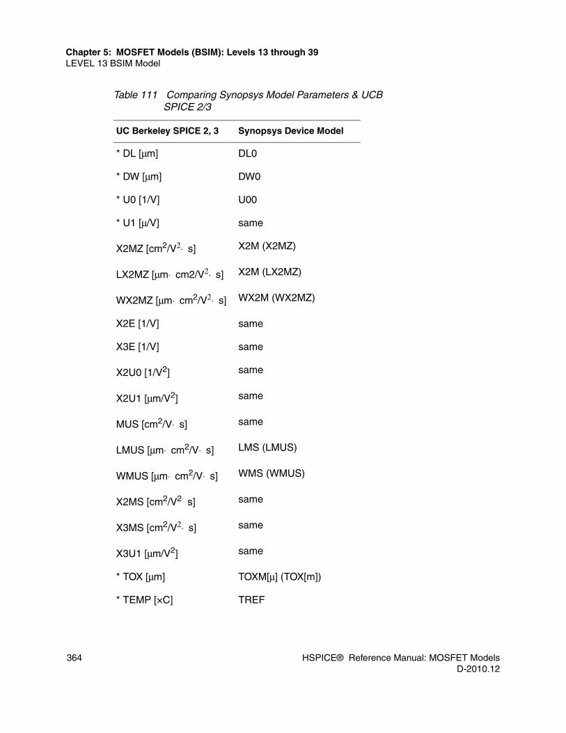
364 HSPICE® Reference Manual: MOSFET ModelsD-2010.12
Chapter 5: MOSFET Models (BSIM): Levels 13 through 39LEVEL 13 BSIM Model
* DL [μm] DL0
* DW [μm] DW0
* U0 [1/V] U00
* U1 [μ/V] same
X2MZ [cm2/V2⋅ s] X2M (X2MZ)
LX2MZ [μm⋅ cm2/V2⋅ s] X2M (LX2MZ)
WX2MZ [μm⋅ cm2/V2⋅ s] WX2M (WX2MZ)
X2E [1/V] same
X3E [1/V] same
X2U0 [1/V2] same
X2U1 [μm/V2] same
MUS [cm2/V⋅ s] same
LMUS [μm⋅ cm2/V⋅ s] LMS (LMUS)
WMUS [μm⋅ cm2/V⋅ s] WMS (WMUS)
X2MS [cm2/V2⋅ s] same
X3MS [cm2/V2⋅ s] same
X3U1 [μm/V2] same
* TOX [μm] TOXM[μ] (TOX[m])
* TEMP [×C] TREF
Table 111 Comparing Synopsys Model Parameters & UCB SPICE 2/3
UC Berkeley SPICE 2, 3 Synopsys Device Model

HSPICE® Reference Manual: MOSFET Models 365D-2010.12
Chapter 5: MOSFET Models (BSIM): Levels 13 through 39LEVEL 13 BSIM Model
In UCB SPICE, you must specify all BSIM model parameters. The Synopsys model provides default values for the parameters.
* VDD [V] VDDM
CGDO [F/m] CGDOM (CGDO)
CGSO [F/m] CGSOM (CGSO)
CGBO [F/m] CGBOM (CGBO)
XPART same
N0 same
* NB NB0
* ND ND0
RSH [ohm/sq] RSHM (RSH)
JS [A/m2] IJS (JS)
PB [V] PJ (PB)
MJ MJ0 (MJ)
* PBSW [V] PJW (PHP)
MJSW MJW (MJSW)
CJ [F/m2] CJM (CJ)
CJSW [F/m] CCJW (CJSW)
* WDF [m] –
* DELL [m] –
Table 111 Comparing Synopsys Model Parameters & UCB SPICE 2/3
UC Berkeley SPICE 2, 3 Synopsys Device Model

366 HSPICE® Reference Manual: MOSFET ModelsD-2010.12
Chapter 5: MOSFET Models (BSIM): Levels 13 through 39LEVEL 13 BSIM Model
Parasitics
ACM >0 invokes parasitic diode models. ACM=0 (default) is SPICE style.
Temperature CompensationThe default TNOM model reference temperature is 25°C, unless you use .OPTION SPICE to set the default TNOM value to 27°C. This option also sets some other SPICE compatibility parameters. You set TNOM in an .OPTION line in the netlist, and you can always use the TREF model parameter to override it locally (that is, for a model). (The model “reference temperature” means that the model parameters were extracted at and are valid at that temperature.
UCB SPICE does not use TNOM (default 27°C) for the BSIM models. Instead, you must specify the TEMP model parameter as both the model reference temperature and the analysis temperature. Analysis at TEMP applies only to thermally-activated exponentials in the model equations. You cannot adjust model parameter values when you use TEMP. Simulation assumes that you extracted the model parameters at TEMP, because TEMP is both the reference and the analysis temperature.
In contrast to UCB SPICE’s BSIM, the Synopsys Level 13 model does provide for temperature analysis. The default analysis temperature is 25°C (and 27°C in UCB SPICE for all model levels except for BSIM as explained in the previous paragraph). Use a .TEMP statement in the netlist to change the analysis temperature.
The Level 13 model provides two temperature coefficients: TCV and BEX. The following equation adjusts the threshold voltage:
This model includes two implementations of the BEX factor. To select a BEX version, use the UPDATE parameter, described in the next section. The mobility in BSIM is a combination of five quantities: MUZ, zmus, z3ms, zx2mz, and zx2ms.
BEX Usage
vth t( ) vth TCV– t tnom–( )⋅=
MUZ t( ) MUZt
tnom-------------⎝ ⎠
⎛ ⎞ BEX⋅=
zmus t( ) zmust
tnom-------------⎝ ⎠
⎛ ⎞ BEX⋅=

HSPICE® Reference Manual: MOSFET Models 367D-2010.12
Chapter 5: MOSFET Models (BSIM): Levels 13 through 39LEVEL 13 BSIM Model
This is equivalent to multiplying the final mobility by the factor:
UPDATE ParameterThe UPDATE parameter selects between variations of the BSIM equations. UPDATE=0 (default) is consistent with UCB SPICE3. UPDATE=3 also is consistent with UCB SPICE3 and BEX usage.
ExplanationsThe normal X2E equation is:
The special X2E equation for UPDATE=1 only, is:
The special X2E equation was developed to match a parameter extraction program. If you use a parameter extraction program, check the equations carefully.
The original U1 equation divides by Leff in microns:
Parameter Description
UPDATE=0 UCB compatible, previous BEX usage
UPDATE=1 Special X2E equation, previous BEX usage
UPDATE=2 Remove 1/Leff in U1 equation, present BEX usage
UPDATE=3 UCB compatible, present BEX usage
zx3ms t( ) zx3mst
tnom-------------⎝ ⎠
⎛ ⎞ BEX⋅=
zx2mz t( ) zx2mzt
tnom-------------⎝ ⎠
⎛ ⎞ BEX⋅=
zx2ms t( ) zx2mst
tnom-------------⎝ ⎠
⎛ ⎞ BEX⋅=
ttnom-------------⎝ ⎠
⎛ ⎞ BEX
xeta zeta zx2e vsb⋅( )– zx3e vds VDDM–( )⋅+=
xeta zera zx2e zphi vsb+( ) zx3e vds VDDM–( )⋅+⋅+=

368 HSPICE® Reference Manual: MOSFET ModelsD-2010.12
Chapter 5: MOSFET Models (BSIM): Levels 13 through 39LEVEL 13 BSIM Model
This is one of the few places where Leff explicitly enters into the BSIM equations; usually, the L-adjustment model parameters (such as LU1) handles the Leff variation.
Physically xu1 should decrease as 1/Leff at long channels, but when dealing with short-channel devices, you can turn off this variation. Set UPDATE=2 to remove the 1/Leff factor in the xu1 equation.
UPDATE=2 introduces the present BEX usage as the 1/Leff removal ability.
UPDATE=3 provides the present BEX using the previous xu1 equation.
IDS and VGS Curves for PMOS and NMOSThe netlists for the IDS and VGS curves for PMOS and NMOS are located in directory $<installdir>/demo/hspice/mos/ml13iv.sp. This file contains examples of the following model parameter and curve descriptions:■ Two Types of Model Parameter Formats Used■ VGS Curves■ GM Test■ GM B CVN7 5 37 0■ .PROCESS PC Filename=M57R■ N-channel Devices■ First Model Parameter Format■ PMOS Model■ Second Model Parameter Format■ N+ Diffusion Layer■ PMOS Model■ Wire Model for Poly and Metal Layers
xu1zu1 zx2u1 vsb⋅( )– zx3u1+ vds VDDM–( )⋅( )
Leff---------------------------------------------------------------------------------------------------------------------------=

HSPICE® Reference Manual: MOSFET Models 369D-2010.12
Chapter 5: MOSFET Models (BSIM): Levels 13 through 39LEVEL 28 Modified BSIM Model
LEVEL 28 Modified BSIM Model
This section lists the LEVEL 28 parameters and equations for the modified BSIM model.
LEVEL 28 Features
The following are the significant features of the LEVEL 28 model. ■ Vertical field dependence of the carrier mobility ■ Carrier velocity saturation ■ Drain-induced barrier lowering ■ Depletion charge sharing by the source and drain ■ Nonuniform doping profile for ion-implanted devices ■ Channel length modulation ■ Subthreshold conduction ■ Geometric dependence of the electrical parameters
LEVEL 28 Model Parameters
MOSFET Level 28 uses the generic MOSFET model parameters described in Chapter 2, Common MOSFET Model Parameters. It also uses the parameters described in this section, which apply only to MOSFET Level 28.
Table 112 Transistor Process Parameters
Name (Alias) Units Default Description
LEVEL 1 MOSFET model level selector. Set this parameter to 28 for this model.
B1 0.0 Lower vdsat transition point
LB1 μm 0.0 Length sensitivity

370 HSPICE® Reference Manual: MOSFET ModelsD-2010.12
Chapter 5: MOSFET Models (BSIM): Levels 13 through 39LEVEL 28 Model Parameters
WB1 μm 0.0 Width sensitivity
B2 1 Upper vdsat transition point
LB2 μm 0.0 Length sensitivity
WB2 μm 0.0 Width sensitivity
CGBO F/m 2.0e-10 Gate-to-bulk parasitic capacitance (F/m of length)
CGDO F/m 1.5e-9 Gate-to-drain parasitic capacitance (F/m of width)
CGSO F/m 1.5e-9 Gate-to-source parasitic capacitance (F/m of width)
ETA0 0.0 Linear vds threshold coefficient
LETA μm 0.0 Length sensitivity
WETA μm 0.0 Width sensitivity
ETAMN 0.0 Minimum linear vds threshold coefficient
LETAMN μm 0.0 Length sensitivity
WETAMN μm 0.0 Width sensitivity
GAMMN V1/2 0.0 Minimum root-vsb threshold coefficient
LGAMN V1/2⋅ μm 0.0 Length sensitivity
WGAMN V1/2⋅ μm 0.0 Width sensitivity
K1 V1/2 0.5 Root-vsb threshold coefficient
LK1 V1/2⋅ μm 0.0 Length sensitivity
Table 112 Transistor Process Parameters
Name (Alias) Units Default Description

HSPICE® Reference Manual: MOSFET Models 371D-2010.12
Chapter 5: MOSFET Models (BSIM): Levels 13 through 39LEVEL 28 Model Parameters
WK1 V1/ 2⋅ μm 0.0 Width sensitivity
K2 0.0 Linear vsb threshold coefficient
LK2 μm 0.0 Length sensitivity
WK2 μm 0.0 Width sensitivity
MUZ cm2/V⋅ s 600 Low drain field first order mobility
LMUZ μm⋅ cm2/V⋅ s 0.0 Length sensitivity
WMUZ μm⋅ cm2/V⋅ s 0.0 Width sensitivity
N0 200 Low field weak inversion gate drive coefficient (value of 200 for N0 disables the weak inversion calculation)
LN0 μm 0.0 Length sensitivity
WN0 μm 0.0 Width sensitivity
NB0 0.0 Vsb reduction to the low field weak inversion gate drive coefficient
LNB μm 0.0 Length sensitivity
WNB μm 0.0 Width sensitivity
ND0 0.0 Vds reduction to the low field weak inversion gate drive coefficient
LND μm 0.0 Length sensitivity
WND μm 0.0 Width sensitivity
PHI0 V 0.7 Two times the Fermi potential
LPHI V⋅ μm 0.0 Length sensitivity
Table 112 Transistor Process Parameters
Name (Alias) Units Default Description

372 HSPICE® Reference Manual: MOSFET ModelsD-2010.12
Chapter 5: MOSFET Models (BSIM): Levels 13 through 39LEVEL 28 Model Parameters
WPHI V⋅ μm 0.0 Width sensitivity
TOXM (TOX) μm (m) 0.02 Gate oxide thickness (if TOXM or TOX >1, uses Angstroms)
U00 1/V 0.0 Gate field mobility reduction factor
LU0 μm/V 0.0 Length sensitivity
WU0 μm/V 0.0 Width sensitivity
U1 1/V 0.0 Drain field mobility reduction factor
LU1 μm/V 0.0 Length sensitivity
WU1 μm/V 0.0 Width sensitivity
VDDM V 5.0 Critical voltage for the high-drain field mobility reduction
VFB0 (VFB) V -0.3 Flatband voltage
LVFB V⋅ μm 0.0 Length sensitivity
WVFB V⋅ μm 0.0 Width sensitivity
WFAC 4 Weak inversion factor
LWFAC μm 0.0 Length sensitivity
WWFAC μm 0.0 Width sensitivity
WFACU 0.0 Second weak inversion factor
LWFACU μm 0.0 Length sensitivity
WWFACU μm 0.0 Width sensitivity
X2E 1/V 0.0 Vsb correction to the linear vds threshold coefficient
LX2E μm/V 0.0 Length sensitivity
Table 112 Transistor Process Parameters
Name (Alias) Units Default Description

HSPICE® Reference Manual: MOSFET Models 373D-2010.12
Chapter 5: MOSFET Models (BSIM): Levels 13 through 39LEVEL 28 Model Parameters
WX2E μm/V 0.0 Width sensitivity
X2M (X2MZ) cm2/V2⋅ s 0.0 Vsb correction to the low field first order mobility
LX2M (LX2MZ) μm⋅ cm2/V2 ⋅ s 0.0 Length sensitivity
WX2M (WX2MZ) μm⋅ cm2/V2 ⋅ s 0.0 Width sensitivity
X2U0 1/V2 0.0 Vsb reduction to the GATE field mobility reduction factor
LX2U0 μm/V2 0.0 Length sensitivity
WX2U0 μm/V2 0.0 Width sensitivity
X2U1 μm/V2 0.0 Vsb reduction to the DRAIN field mobility reduction factor
LX2U1 μm2/V2 0.0 Length sensitivity
WX2U1 μm2/V2 0.0 Width sensitivity
X33M cm2/V2⋅ s 0.0 Gate field reduction of X3MS
LX33M μm⋅ cm2/V2⋅ s 0.0 Length sensitivity
WX33M μm⋅ cm2/V2⋅ s 0.0 Width sensitivity
X3E 1/V 0.0 Vds correction to the linear vds threshold coefficient
LX3E μm/V 0.0 Length sensitivity
WX3E μm/V 0.0 Width sensitivity
X3MS cm2/V2⋅ s 5.0 Vds correction for the high-drain field mobility
Table 112 Transistor Process Parameters
Name (Alias) Units Default Description

374 HSPICE® Reference Manual: MOSFET ModelsD-2010.12
Chapter 5: MOSFET Models (BSIM): Levels 13 through 39LEVEL 28 Model Parameters
Notes:■ When you read parameter names, be careful about the difference in
appearance between the capital letter O and the number zero (0). ■ Use NMOS conventions to specify all Level 28 parameters, even for
PMOS—for example, ETA0=0.02, not ETA0=-0.02.■ You can use the WL-product sensitivity parameter for any parameter with an
L and W sensitivity. Replace the leading “L” of the L sensitivity parameter name with a “P”.
LX3MS μm⋅ cm2/V2⋅ s 0.0 Length sensitivity
WX3MS μm⋅ cm2/V2⋅ s 0.0 Width sensitivity
X3U1 1/V2 0.0 Vds reduction to the drain field mobility reduction factor
LX3U1 μm/V2 0.0 Length sensitivity
WX3U1 μm/V2 0.0 Width sensitivity
XPART 1.0 Selects the coefficient for sharing the gate capacitance charge
Table 113 Temperature Parameters
Name (Alias) Units Default Description
BEX -1.5 Temperature exponent for the MUZ, X2M, X3MS, and X33M mobility parameters
FEX 0.0 Temperature exponent for the U1 mobility reduction factor
TCV V/° K 0.0 Flat-band voltage temperature coefficient
Table 112 Transistor Process Parameters
Name (Alias) Units Default Description

HSPICE® Reference Manual: MOSFET Models 375D-2010.12
Chapter 5: MOSFET Models (BSIM): Levels 13 through 39LEVEL 28 Model Parameters
Sensitivity Factors of Model ParametersFor transistors, drop the 0 from the end of the parameter name, and add one of the following product sensitivity factors for a basic electrical parameter:■ L (channel length)■ W (channel width)■ WL (width and length)
For example, the VFB0 sensitivity factors are LVFB, WVFB, and PVFB. If A0 is a basic parameter, LA, WA and PA are the corresponding sensitivity factors for this parameter (you cannot use the SCALM option to scale LA, WA, and PA). Then the model uses the following general formula to obtain the parameter value.
The left side of the equation represents the effective model parameter value after you adjust the device size. All effective model parameters are in lower case and start with the z character, followed by the parameter name.
Specify LA and WA in units of microns times the units of A0. Specify PA in units of square microns times the units of A0.
If you set LREF or WREF=0, you effectively set the parameter value to infinity. This is the default.
Example
za A0 LA1
Leff---------- 1
LREFeff----------------------– WA
1Weff------------ 1
WREFeff------------------------–⋅+⋅+=
PA1
Leff---------- 1
LREFeff----------------------–
1Weff------------ 1
WREFeff------------------------–⋅ ⋅
VFB0 0.350v–=
LVFB 0.1vμ–=
WVFB 0.08v μ⋅=
Leff 1 10 6–⋅ m 1μ= =
Weff 2 10 6–⋅ m 2μ= =
LREFeff 2 10 6– m⋅ 2μ= =
WREFeff 1 10 5–⋅ m 10μ= =

376 HSPICE® Reference Manual: MOSFET ModelsD-2010.12
Chapter 5: MOSFET Models (BSIM): Levels 13 through 39LEVEL 28 Model Equations
LEVEL 28 Model Equations
The LEVEL 28 model equations follow.
Effective Channel Length and WidthThe effective channel length and width for Level 28 is consistent with the LEVEL 3 model. L, W, and the M multiplier are from the .MODEL statement in the netlist. SCALE and SCALM are options. If you do not specify any scaling options or multipliers, then:
Leff=L+XL-2⋅ LD Weff=W+XW-2⋅ WD
Note: If you specify LDAC and WDAC in the .MODEL statement, Leff=L+XL-2⋅ LDAC Weff=W+XW-2⋅ WDAC
Lscaled=L⋅ SCALEWscaled=W⋅ SCALEXLscaled=XL⋅ SCALMLDscaled=LD⋅ SCALMXWscaled=XW⋅ SCALMWDscaled=WD⋅ SCALMLeff=Lscaled⋅ LMLT+XLscaled-2⋅ LDscaledLREFeff=LREFscaled⋅ LMLT+XLREFscaled-2⋅ LDscaledWeff=M⋅ (Wscaled⋅ WMLT+XWREFscaled-2⋅ WDscaled)WREFeff=MÞ (WREFscaled⋅ WMLT+XWscaled-2⋅ WDscaled)
zvfb VFB0 LVFB1
Leff---------- 1
LREFeff----------------------–⎝ ⎠
⎛ ⎞⋅ WVFB1
Weff------------ 1
WREFeff------------------------–⎝ ⎠
⎛ ⎞⋅+ +=
zvfb 0.35v– 0.1v– μ 11μ------ 1
2μ------–⎝ ⎠
⎛ ⎞⋅ ⋅ 0.08v μ 12μ------ 1
10μ---------–⎝ ⎠
⎛ ⎞⋅ ⋅+ +=
zvfb 0.35v– 0.05v– 0.032v+=
zvfb 0.368v–=

HSPICE® Reference Manual: MOSFET Models 377D-2010.12
Chapter 5: MOSFET Models (BSIM): Levels 13 through 39LEVEL 28 Model Equations
Threshold VoltageEffective model parameter values for the threshold voltage, after you adjust the device size, are zphi, zvfb, zk1, zk2, zeta, zx2e, zx3e, zgammn, and zetamn. Simulation calculates these values from the PHI0, VFB0, K1, K2, ETA0, X2E, X3E, GAMMN, and ETAMN model parameters, and from their respective length and width sensitivity parameters.
xbs=(zphi-vbs)1/2
xeta=zeta+zx2e⋅ vbs+zx3e⋅ vds
vth=zvfb + zphi + zk1⋅ xbs - zk2⋅ xbs2-xeta⋅ vds
This equation is quadratic in xbs and vds. It is joined to linear equations at d(vth)/d(xbs)=zgammn and at d(vth)/d(vds)=-zetamn, which prevents the quadratics from going in the wrong direction.
Both gammn and etamn default to zero, and typically do not affect behavior in the normal operating region.
Effective MobilityThe effective model parameter values for mobility, after you adjust the device size, are zmuz, zx2m, zx3m, zx33m, zu0, and zx2u0. Simulation calculates these values from the MUZ, X2M, X3m, X33M, U00, and X2U0 model parameters, and from their respective length and width sensitivity parameters.
,
,
vgst vgs vth–=
meff zmuz zx2m vbs⋅+( )=
cx3mszx3ms
muz zx33m vgst⋅+( )-----------------------------------------------------=
1 cx3ms VDDM vds VDDM(–+ VDDM vds vds )1 2⁄⋅+⋅( )⋅+( )
xu0 zu0 zx2u0 vbs⋅+=
ueff
meff
1 xu0 vgst⋅+( )---------------------------------------= beta ueff COX
Weff
Leff----------⋅ ⋅=

378 HSPICE® Reference Manual: MOSFET ModelsD-2010.12
Chapter 5: MOSFET Models (BSIM): Levels 13 through 39LEVEL 28 Model Equations
Saturation Voltage (vdsat)The effective model parameter values for the saturation voltage, after you adjust the device size, are zu1, zx2u1, and zx3u1. Simulation calculates these values from the U1, X2U1, and X3U1 model parameters, and from their length and width sensitivity parameters.
,
,
This vds value generates the partial derivative of:
In the preceding equation, vds=zero.
Transition PointsThe effective model parameter values for the transition points, after you adjust the device size, are zb1 and zb2. Simulation calculates these values from the B1 and B2 model parameters, and from their respective length and width sensitivity parameters.
,
Strong Inversion CurrentFor vds < v1:
xbs zphi vbs–( )1 2⁄= g 1
1
1.744 0.8364 xbs2⋅+( )
-----------------------------------------------------------–=
body1 g zk1⋅+
2 xbs⋅( )----------------------------= xu1 zu1 vbs zx2u1⋅+=
rx body2
zu1 2 body vgst zx3u1 4 vgst2⋅ ⋅+⋅ ⋅ ⋅+( )
1 2⁄=
vdsat
2 vgst⋅body rx+( )
-----------------------------=
f vds vgst vbs, ,( ) vgst body 2⁄ vds⋅–( )vds
1 xu1 zx3u1 vds⋅+( )+ vds⋅( )-------------------------------------------------------------------------------⋅=
v1 vdsat zb1vdsat
1 vdsat+--------------------⋅–= v2 vdsat zb2 vgst⋅+=

HSPICE® Reference Manual: MOSFET Models 379D-2010.12
Chapter 5: MOSFET Models (BSIM): Levels 13 through 39LEVEL 28 Model Equations
The vds derivative varies approximately linearly between v1 and v2.
For vds>v2, ids is a function of beta and vgst only. If zb1 and zb2 are both positive, their main effect is to increase the saturation current.
Weak Inversion CurrentThe effective model parameter values for weak inversion current, after you adjust the device size, are zn0, znb, znd, zwfac, and zwfacu. Simulation calculates these values from the N0, ND0, NB0, WFAC, and WFACU model parameters, and from their respective length and width sensitivity parameters.
Simulation calculates the weak inversion current when zn0 is less than 200, and adds it to the strong inversion current:
In deep subthreshold:
,
zwfac and zwfacu control the modification of this formula near the threshold. Just above threshold, the device is in saturation:
Iweak needs an xweak2 term to cancel the kink in gm at the threshold. Then Iweak goes to zero for xweak>A0, which is at a small voltage above the threshold. Iweak has four regions.
xweak < -zwfac+A0
-zwfac+A0 < xweak < 0
Ids beta vgst body 2⁄ vds⋅–( )vds
1 zu1 zx3u1 vds⋅+( )+ vds⋅( )------------------------------------------------------------------------------⋅ ⋅=
Itotal Istrong Iweak 1 expvds–
vtherm------------------
⎝ ⎠⎛ ⎞–⎝ ⎠
⎛ ⎞⋅+=
xn zn0 znb vbs znd vds⋅+⋅+=
vthermKTQ
-------= xweakvgs vt–( )
xn vtherm⋅( )------------------------------------=
Iweak const exp xweak( )⋅=
Istrong const xweak2⋅=
Iweak const exp xweak( )⋅=
Iweak const exp xweak const wf⋅–( )⋅=

380 HSPICE® Reference Manual: MOSFET ModelsD-2010.12
Chapter 5: MOSFET Models (BSIM): Levels 13 through 39LEVEL 39 BSIM2 Model
In the preceding equation, wf is the integral with respect to the xweak value of:
0 < xweak < A0
A0 < xweak
A0, and the constants in the preceding equations, are not model parameters. Continuity conditions, at the boundaries between regions, uniquely determine these constants.
LEVEL 39 BSIM2 Model
BSIM2 (Berkeley Short-Channel IGFET Model 2) is the LEVEL 39 MOSFET model. The Synopsys implementation of this model is based on Berkeley SPICE 3E2.
To provide input to the Level 39 device model, assign the model parameters as for other device models. You can use a tabular model entry without model parameter names in BSIM1, but not in BSIM2.
LEVEL 39 Model ParametersMOSFET Level 39 uses the generic MOSFET model parameters described in Chapter 5, MOSFET Models (BSIM): Levels 13 through 39. It also uses the parameters described in this section, which apply only to MOSFET Level 39.
This section lists the BSIM2 parameters, their units, their defaults (if any) in the Level 39 MOSFET model, and their descriptions. Table 114 lists 47 BSIM2-specific parameters. The Synopsys model does not use three of the parameters (TEMP, DELL, and DFW). The width and length sensitivity parameters are associated with the remaining parameters, except the first six (TOX, VDD, VGG, VBB, DL, and DW). So the total parameter count is 120. (Unlike Berkeley SPICE, the Synopsys Level 39 MOSFET model has L and W
dwfxweak zwfac A0–+( )2
1 xweak zwfac A0–+ +( ) 1 zwfacu xweak zwfac A0–+( )⋅+( ) ][-----------------------------------------------------------------------------------------------------------------------------------------------------------------------=
Iweak same formula as in region 2( ) const xweak2⋅–=
Iweak 0=

HSPICE® Reference Manual: MOSFET Models 381D-2010.12
Chapter 5: MOSFET Models (BSIM): Levels 13 through 39LEVEL 39 BSIM2 Model
sensitivity for MU0). This count does not include the generic MOS parameters or the WL-product sensitivity parameters, which are Synopsys enhancements.
Table 114 BSIM2 Model Parameters
Name (Alias) Units Default Description
TOX m 0.02 Gate oxide thickness (assumes that TOX>1 is in Angstroms)
TEMP C - Not used in Level 39 (see Compatibility Notes on page 388)
VDD V 5 Drain supply voltage (NMOS convention)
VGG V 5 Gate supply voltage (NMOS convention)
VBB V -5 Body supply voltage (NMOS convention)
DL m 0 Channel length reduction
DW m 0 Channel width reduction
VGHIGH V 0 Upper bound of the weak-strong inversion transition region
VGLOW V 0 Lower bound of the weak-strong inversion transition region
VFB V -0.3 Flat band voltage
PHI V 0.8 Surface potential
K1 V-1 0.5 Body effect coefficient
K2 - 0 Second-order body effect coefficient (for nonuniform channel doping)
ETA0 - 0 Drain-induced barrier lowering coefficient
ETAB V-1 0 Sensitivity of the drain-induced barrier lowering coefficient to Vbs
MU0 cm2/V⋅ s 400 Low-field mobility
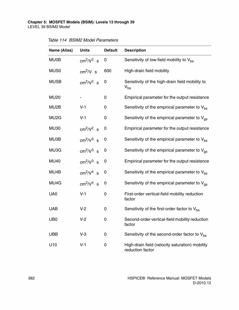
382 HSPICE® Reference Manual: MOSFET ModelsD-2010.12
Chapter 5: MOSFET Models (BSIM): Levels 13 through 39LEVEL 39 BSIM2 Model
MU0B cm2/V2⋅ s 0 Sensitivity of low-field mobility to Vbs
MUS0 cm2/V⋅ s 600 High-drain field mobility
MUSB cm2/V2⋅ s 0 Sensitivity of the high-drain field mobility to Vbs
MU20 - 0 Empirical parameter for the output resistance
MU2B V-1 0 Sensitivity of the empirical parameter to Vbs
MU2G V-1 0 Sensitivity of the empirical parameter to Vgs
MU30 cm2/V2⋅ s 0 Empirical parameter for the output resistance
MU3B cm2/V3⋅ s 0 Sensitivity of the empirical parameter to Vbs
MU3G cm2/V3⋅ s 0 Sensitivity of the empirical parameter to Vgs
MU40 cm2/V3⋅ s 0 Empirical parameter for the output resistance
MU4B cm2/V4⋅ s 0 Sensitivity of the empirical parameter to Vbs
MU4G cm2/V4⋅ s 0 Sensitivity of the empirical parameter to Vgs
UA0 V-1 0 First-order vertical-field mobility reduction factor
UAB V-2 0 Sensitivity of the first-order factor to Vbs
UB0 V-2 0 Second-order vertical-field mobility reduction factor
UBB V-3 0 Sensitivity of the second-order factor to Vbs
U10 V-1 0 High-drain field (velocity saturation) mobility reduction factor
Table 114 BSIM2 Model Parameters
Name (Alias) Units Default Description

HSPICE® Reference Manual: MOSFET Models 383D-2010.12
Chapter 5: MOSFET Models (BSIM): Levels 13 through 39LEVEL 39 BSIM2 Model
Specify all BSIM2 parameters according to the NMOS convention, even for a PMOS model. Examples: VDD=5, not -5; VBB=-5, not 5; and ETA0=0.02, not -0.02. See Compatibility Notes on page 388.
U1B V-2 0 Sensitivity of the mobility reduction factor to Vbs
U1D V-2 0 Sensitivity of the mobility reduction factor to Vds
N0 - 0.5 Subthreshold swing coefficient
NB V1/2 0 Sensitivity of the subthreshold swing to Vbs
ND V-1 0 Sensitivity of the subthreshold swing to Vds
VOF0 - 0 Threshold offset (normalized to NKT/q) for the subthreshold
VOFB V-1 0 Sensitivity of the offset to Vbs
VOFD V-1 0 Sensitivity of the offset to Vds
AI0 - 0 Impact ionization coefficient
AIB V-1 0 Sensitivity of the impact ionization coefficient to Vbs
BI0 V 0 Impact ionization exponent
BIB - 0 Sensitivity of the impact ionization exponent to Vbs
DELL m - Length reduction of the source drain diffusion (not used in the Level 39 MOSFET model)
WDF m - Default width (not used in the Level 39 MOSFET model); use .OPTION DEFW=# in the netlist instead
Table 114 BSIM2 Model Parameters
Name (Alias) Units Default Description

384 HSPICE® Reference Manual: MOSFET ModelsD-2010.12
Chapter 5: MOSFET Models (BSIM): Levels 13 through 39LEVEL 39 BSIM2 Model
The Level 39 MOSFET model also includes the JSW[A/m] source/drain bulk diode sidewall reverse saturation current density.
Other Device Model Parameters that Affect BSIM2You must specify the following MOSFET model parameters before you can use some Synopsys enhancements, such as■ LDD-compatible parasitics.■ Adjusts the model parameter geometry, relative to a reference device.■ Impact ionization modeling with bulk-source current partitioning.■ Element temperature adjustment of the key model parameters.
This is a partial list. For complete information, see the following:■ Calculating Effective Length and Width for AC Gate Capacitance on
page 691■ Drain and Source Resistance Model Parameters on page 697■ MOSFET Impact Ionization on page 744
.MODEL VERSION Changes to BSIM2 Models on page 390 describes how the VERSION parameter in the .MODEL statement changes the BSIM2 model, depending on the model version number.
LEVEL 39 Model EquationsIn the following expressions, model parameters are in all upper case Roman. These expressions assume that you have already adjusted all model parameters for geometry, and that you have already adjusted parameters without a trailing 0 for the bias as appropriate. The exceptions are U1 and N for which the following equations explicitly calculate the bias dependences.
Threshold voltage, Vth
The following equation calculates the vbi value used in the preceding equation:
Strong inversion (Vgs > Vth + VGHIGH)
Linear region (Vds<Vdsat) drain-source current IDS:
Vth Vbi K1 PHI Vbs– K2 PHI Vbs–( )– ETA Vds⋅–+=
Vbi VFB PHI+=

HSPICE® Reference Manual: MOSFET Models 385D-2010.12
Chapter 5: MOSFET Models (BSIM): Levels 13 through 39LEVEL 39 BSIM2 Model
The following equations calculate values used in the preceding equation:
In the preceding equations, (x) is the usual unit step function:
,
Saturation (Vds > Vdsat) drain-source current, IDS:
IDS
β' Vgs Vtha2---Vds––⎝ ⎠
⎛ ⎞ Vds
1 UA Vgs Vth–( ) UB Vgs V– th( )2U1 Vds⋅+ + +
-----------------------------------------------------------------------------------------------------------------=
Vdsat
Vgs Vth–
a K--------------------- ,=
K1 Vc 1 2Vc++ +
2--------------------------------------------,=
Vc
U1S Vgs Vth–( )
a 1 UA Vgs Vth–( ) UB Vgs V– th( )2+ +[ ]
-------------------------------------------------------------------------------------------- ,=
U1S U10 U1B Vbs,⋅+=
U1 U1S 1 Θ Vdsat Vds–( )U1D Vds Vdsat–( )2
Vdsat2
----------------------------------------------–=
Θ
β' β0 β1 MU2Vds
Vdsat------------⎝ ⎠
⎛ ⎞tanh β3Vds β4Vds2–+ +=
β0
Weff
Leff----------MU Cox,⋅=
β1 βS β0 β3VDD+ β4VDD2–( ),–=
βi
Weff
Leff----------MUi Cox, i⋅ S 3 4,, ,= = a 1
gK1
2 PHI Vbs–-------------------------------- ,+=
g 11
1.744 0.8364 PHI Vbs–( )+------------------------------------------------------------------ –=
IDS
β' Vgs Vth–( )2
2aK 1 UA Vgs Vth–( ) UB Vgs V– th( )2+ +[ ]
---------------------------------------------------------------------------------------------------- 1 f+( )⋅=

386 HSPICE® Reference Manual: MOSFET ModelsD-2010.12
Chapter 5: MOSFET Models (BSIM): Levels 13 through 39LEVEL 39 BSIM2 Model
In the preceding equation, the f impact ionization term is:
Weak Inversion (Vgs<Vth+VGLOW; [VGLOW<0])
Subthreshold drain-source current, Ids:
The following equations calculate the Vtm and N values used in the preceding equation:
and
Strong inversion-to-weak inversion transition region (Vth +VGLOW£ Vgs £th +VGHIGH)
The preceding equation replaces Vgst=Vgs - Vth in the linear or saturation drain currents, based on Vdsat (Vgeff).
At the lower boundary (Vgs-Vth=VGLOW), the saturation equation is valid for all
Vds (that is, Vdsat (Vgeff(VGLOW)) 0) to allow a match to the above subthreshold equation.
To internally determine the Cj coefficients of the Vgeff cubic spline, the IDS and dIds/dVgs conditions must both be continuous at the Vgs=Vth + VGLOW and Vgs=Vth + VGHIGH boundaries.
Effective Length and WidthIf DL is nonzero
Otherwise:
f AI eBI–
Vds Vdsat–-------------------------
⋅ .=
IDS β′ Vtm2 exp
Vgs Vth–
N Vtm⋅--------------------- VOFF+⎝ ⎠
⎛ ⎞⋅ ⋅ 1 expVds
Vtm--------–⎝ ⎠
⎛ ⎞– 1 f+( )⋅ ⋅=
VtmkTq
------= N N0NB
PHI Vbs–----------------------------- ND Vds⋅+ +=
Vgeff Vgst( ) CjVgstj
j 0=
3
∑=
≈
Leff Lscaled LMLT DL–⋅=
LREFeff LREFscaled LMLT⋅ DL–=

HSPICE® Reference Manual: MOSFET Models 387D-2010.12
Chapter 5: MOSFET Models (BSIM): Levels 13 through 39LEVEL 39 BSIM2 Model
If DW is nonzero
Otherwise:
Geometry and Bias of Model ParametersMost of the BSIM2 parameters include width and length sensitivity parameters. You can also specify Synopsys-proprietary WL-product sensitivity parameters. If P is a parameter, then its associated width, length, and WL-product sensitivity parameters are WP, LP, and PP.
The value of the P’ parameter, adjusted for width, length, and WL-product, is:
Berkeley SPICE does not use the WREF and LREF terms. They are effectively infinite, which is the default in the Level 39 MOSFET model.
The following BSIM2 parameters do not have associated geometry-sensitivity parameters:
TOXTEMP (not used)VDDVGGVBBDLDW
Leff Lscaled LMLT⋅ XLscaled 2 LDscaled⋅–+=
LREFeff LREFscaled LMLT⋅ XLREFscaled 2 LDscaled⋅–+=
Weff Wscaled WMLT⋅ DW–( ) M⋅=
WREFeff WREFscaled WMLT⋅ DW–( ) M⋅=
Weff Wscaled WMLT⋅ XW 2 WDscaled⋅–+( ) M⋅=
WREFeff WREFscaled WMLT⋅ XWREFscaled 2 WDscaled⋅–+( ) M⋅=
P' P WP1
Weff---------- 1
WREFeff----------------------–⎝ ⎠
⎛ ⎞ LP1
Leff-------- 1
LREFeff--------------------–⎝ ⎠
⎛ ⎞⋅+⋅+=
PP1
Weff---------- 1
WREFeff----------------------–⎝ ⎠
⎛ ⎞ 1Leff-------- 1
LREFeff--------------------–⎝ ⎠
⎛ ⎞⋅ ⋅+

388 HSPICE® Reference Manual: MOSFET ModelsD-2010.12
Chapter 5: MOSFET Models (BSIM): Levels 13 through 39LEVEL 39 BSIM2 Model
BSIM2 parameters ending in 0 are valid at zero bias, and they have associated bias sensitivities, listed in the BSIM2 parameter table.
If PB, PD, and PG are the geometry-adjusted vbs-, vds-, and vgs- sensitivity parameters, and if they are associated with the P0 geometry-adjusted zero-bias parameter, then the following equation calculates the P bias-dependent parameter:
The exceptions are the U1 velocity saturation factor and the N subthreshold swing coefficient. Modeling Guidelines, Removing Mathematical Anomalies on page 395 shows expressions for their bias dependences.
Compatibility Notes
SPICE3 FlagIf you specify the SPICE3=0 (default) model parameter, certain Synopsys corrections to the BSIM2 equations are effective. If you set the SPICE3 value to 1, the equations are as faithful as possible to the BSIM2 equations for SPICE3E2. Even in this mode, certain numerical problems have been addressed and should not normally be noticeable.
TemperatureThe default model reference temperature (TNOM) is 25°C in the Level 39 MOSFET model, unless you set .OPTION SPICE, which sets the TNOM default to 27° C. This option also sets some other SPICE compatibility parameters. In the Level 39 model, you set TNOM in an .OPTION line in the netlist; to override this locally (that is, for a model), use the TREF model parameter. (“Reference temperature” means that the model parameters were extracted at, and are therefore valid at, that temperature.)
UCB SPICE 3 does not use TNOM (default 27° C) for the BSIM models. Instead, you must specify the TEMP model parameter as both the model reference temperature and the analysis temperature. Analysis at TEMP applies only to thermally-activated exponentials in the model equations. You cannot adjust the model parameter values if you use TEMP. Simulation assumes that you extracted the model parameters at TEMP, because TEMP is both the reference and analysis temperature.
P P0 PB Vbs⋅ PD Vds⋅ PG Vgs⋅+ + +=
HSPICE® Reference Manual: MOSFET Models 389D-2010.12
Chapter 5: MOSFET Models (BSIM): Levels 13 through 39LEVEL 39 BSIM2 Model
For model levels other than 4 (BSIM1) and 5 (BSIM2) in UCB SPICE3, simulation adjusts the key model parameters for the difference between TEMP (default 27°C) and TNOM. To specify TEMP in the netlist, use .TEMP # as in the Level 39 MOSFET model.
In contrast to UCB SPICE’s BSIM models, the Synopsys Level 39 MOSFET model does provide for temperature analysis. The default analysis temperature is 25°C in the Level 39 model. Set .TEMP # in your netlist to change the analysis temperature (you cannot use TEMP as a model parameter). The Level 39 MOSFET model adjusts the temperature of the key model parameters as explained in Temperature Effect on page 357.
ParasiticsACM > 0 invokes the MOS source-drain parasitics in the Level 39 MOSFET device model. ACM=0 (default) is SPICE style. See Synopsys Device Model Enhancements on page 392.
Selecting Gate CapacitanceCAPOP=39 selects the BSIM2 charge-conserving capacitance model as shipped with Berkeley SPICE 3E2. This is the default selection if you set SPICE3=1. ■ XPART (charge-sharing flag) is currently not a BSIM2 model parameter,
despite its specification in the sample BSIM2 input decks shipped with Berkeley SPICE 3E. It appears that its use in SPICE 3E was as a printback debug aid.
■ Saturation charge sharing appears to be fixed at 60/40 (S/D) in the BSIM2 capacitance model. For the charge equations, see Charge-based Gate Capacitance Model (CAPOP=39) on page 391. See also Modeling Guidelines, Removing Mathematical Anomalies on page 395.
You can choose other CAPOP values. CAPOP=13 (recommended) selects the BSIM1-based charge-conserving capacitance model for the MOSFET LEVEL 13 (BSIM1) or LEVEL 28 (modified BSIM1) device models. This option is the default selection if SPICE3=0. If you use this capacitance model, you can use the XPART or XQC model parameters to adjust charge sharing. See LEVEL 13 BSIM Model on page 345 for more information.

390 HSPICE® Reference Manual: MOSFET ModelsD-2010.12
Chapter 5: MOSFET Models (BSIM): Levels 13 through 39LEVEL 39 BSIM2 Model
Unused ParametersThe Level 39 MOSFET model does not use the DELL (S/D diode length reduction) and WDF (default device width) SPICE model parameters. SPICE 3E does not use the DELL function. You can specify a default width in the Level 39 MOSFET model, on the .OPTION line as DEFW (which defaults to 100μ).
.MODEL VERSION Changes to BSIM2 ModelsThe Level 39 MOSFET model provides a VERSION parameter to the .MODEL statement, which lets you move LEVEL 13 BSIM and LEVEL 39 BSIM2 models between device model versions. Use the VERSION parameter in a LEVEL 13 .MODEL statement. Table 115 lists the changes in the BSIM model.
Preventing Negative Output ConductanceThe Level 39 MOSFET model internally protects against conditions in the LEVEL 13 model that cause convergence problems due to negative output conductance. This model imposes the following constraints:
Simulation imposes these constraints after adjusting the length and width and setting the VBS dependence. This feature loses some accuracy in the saturation region, particularly at high Vgs.
Table 115 BSIM2 Model Features by Version Number
Model Version Effect of VERSION on BSIM2 Model
92A LEVEL 39 BSIM2 model introduced: no changes
92B No changes
93A Introduced gds constraints, fixed a defect in the WMU3B parameter, and introduced a defect in the MU4 parameter
93A.02 Introduced the VERSION parameter, and fixed an MU4 parameter defect
95.1 Fixed defects that caused PMUSB, LDAC, and WDAC parameter problems, fixed the GMBS defect if you used gds constraints
96.1 Limited ETA + ETAB ⋅ vb5≥0
MU2 0≥ ND 0≥ AI 0≥

HSPICE® Reference Manual: MOSFET Models 391D-2010.12
Chapter 5: MOSFET Models (BSIM): Levels 13 through 39LEVEL 39 BSIM2 Model
Consequently, you might need to requalify the BSIM2 models in the following situations:■ Devices exhibit self-heating during characterization, which causes declining
Ids at high Vds. This does not occur if the device characterization measurement sweeps Vds.
■ The extraction technique produces parameters that result in negative conductance.
■ This model simulates the voltage outside the device’s characterized range.
Charge-based Gate Capacitance Model (CAPOP=39)The BSIM2 gate capacitance model conserves charge and has non-reciprocal attributes. Using charges as state variables guarantees charge conservation. Charge partitioning is fixed at 60/40 (S/D) in saturation and is 50/50 in the linear region. Qs=-(Qg+Qd+Qb) in all regions.
Accumulation region (Vgs<Vbs + VFB)
Subthreshold region (Vbs + VFB<Vgs<Vth + VGLOW)
Saturation region (Vds > Vdsat)
The following equations calculate values used in the preceding equation:
Qg CoxWeff Leff Vgs Vbs– VFB–( )⋅=
Qb Q– g=
Qd 0=
Qg CoxWeff Leff Vgs Vbs– VFB–( )⋅=
1Vgs Vbs– VFB–
Vgs Vbs– VFB– Vgst–------------------------------------------------------- 1
3---
Vgs Vbs– VFB–
Vgs Vbs– VFB– Vgst–-------------------------------------------------------
⎩ ⎭⎨ ⎬⎧ ⎫
2
+–
Qb Q– g=
Qd 0=
Qg23---CoxWeff Leff Vgst Qbulk+⋅ ⋅=

392 HSPICE® Reference Manual: MOSFET ModelsD-2010.12
Chapter 5: MOSFET Models (BSIM): Levels 13 through 39LEVEL 39 BSIM2 Model
Linear region :
,
Synopsys Device Model EnhancementsIn the following expressions, model parameters are in all upper case Roman. Simulation assumes that you have already adjusted all model parameters without a trailing 0 for both geometry and bias as appropriate.
Temperature EffectsLEVEL=39 enforces TLEV=1. You cannot currently use any other TLEV value. The following equation adjusts the threshold voltage for Level 39 TLEV=1:
The following equations calculate values used in the preceding equation:
Qbulk13---CoxWeff Leff Vth Vbs– VFB–[ ]⋅=
Qb Qbulk–=
Qd410------ 2
3---CoxWeff Leff Vgst⋅ ⋅⋅–
415------–⎝ ⎠
⎛ ⎞ CoxWeff Leff Vgst⋅⋅= =
Vds Vdsat<( )
Qg23---CoxWeff Leff Vgst⋅ ⋅
3 1Vds
Vdsat------------–⎝ ⎠
⎛ ⎞ Vds
Vdsat------------⎝ ⎠
⎛ ⎞2
+
2Vds
Vdsat------------–
--------------------------------------------------------- Qbulk+⋅=
Qb Qbulk–= Qd13---– CoxWeff Leff Vgst⋅ ⋅=
3 1Vds
Vdsat------------–⎝ ⎠
⎛ ⎞ Vds
Vdsat------------⎝ ⎠
⎛ ⎞2
+
2Vds
Vdsat------------–
---------------------------------------------------------
Vds
Vdsat------------ 1
Vds
Vdsat------------–⎝ ⎠
⎛ ⎞ 0.2Vds
Vdsat------------⎝ ⎠
⎛ ⎞2
+
2Vds
Vdsat------------–⎝ ⎠
⎛ ⎞ 2--------------------------------------------------------------------------+ Qbulk+
Vth T( ) Vbi T( ) K1 φ T( ) Vbs– K2 φ T( ) Vbs–( ) ETA Vds⋅–⋅–⋅+=
Vbi T( ) Vto T( ) K1 φ T( ) K2 φ T( )⋅+⋅–=

HSPICE® Reference Manual: MOSFET Models 393D-2010.12
Chapter 5: MOSFET Models (BSIM): Levels 13 through 39LEVEL 39 BSIM2 Model
In the preceding equations, the nominal-temperature, zero-bias threshold voltage is:
Simulation calculates φ(T) according to the specified TLEVC value.
The following equation adjusts the mobility:
UIS adjusts the velocity saturation:
This model also includes all of the usual Synopsys model adjustments to capacitances, parasitics, diodes, and resistors.
Alternate Gate Capacitance ModelSelect CAPOP=13 for the charge-conserving capacitance model, widely used with LEVEL=13 (BSIM1) and LEVEL=28 (improved BSIM1). See LEVEL 13 BSIM Model on page 345 for more details.
Impact IonizationTo select impact ionization modeling (instead of BSIM2), keep the AI0=0 value, and specify the ALPHA [ALPHA ⋅ (Vds - Vdsat) replaces AI in equation for f in the BSIM2 equations section], VCR (replaces BI), and IIRAT (multiplies f) model parameters.
Synopsys impact ionization modeling differs from BSIM2 modeling in two ways:■ A bias term (Vds - Vdsat) multiplies the exponential and ALPHA values.
■ You can use the IIRAT model parameter to partition the impact ionization component of the drain current, between the source and the bulk. IIRAT multiplies f in the saturation Ids equation. Thus, the IIRAT fraction of the
Vto T( ) Vto TCV T Tnom–( )⋅–=
Vto Vbi K1 PHI K2 PHI⋅–⋅+=
VFB PHI K1 PHI K2 PHI ,⋅–⋅+ +=
μ T( ) μ Tnom( ) TTnom-----------⎝ ⎠
⎛ ⎞ BEXwhere μ⋅ β'
Cox Weff Leff⁄( )---------------------------------------- .= =
U1S T( ) U1ST
Tnom-----------⎝ ⎠
⎛ ⎞ FEX⋅=

394 HSPICE® Reference Manual: MOSFET ModelsD-2010.12
Chapter 5: MOSFET Models (BSIM): Levels 13 through 39LEVEL 39 BSIM2 Model
impact ionization current goes to the source, and the 1-IIRAT fraction goes to the bulk, adding to IDB. IIRAT defaults to zero (that is, 100% of impact ionization current goes to the bulk).
BSIM2’s impact ionization assumes that all of the impact ionization current is part of Ids. In other words, it flows to the source. This assumption can lead to inaccuracies, for example, in cascode circuits.
Parasitic Diode for Proper LDD ModelingThe Level 39 MOSFET model includes alternative MOS parasitic diodes to replace SPICE-style MOS parasitic diodes. You can use these alternatives to geometrically scale the parasitics with MOS device dimension, properly modeling the LDD parasitic resistances, shared sources and drains, and select different diode sidewall capacitances along the gate edge and field edge.
To select the MOS parasitic diode, use the ACM model parameter. ■ ACM=0 (default) chooses SPICE style. The alternatives likely to be of most
interest to the BSIM2 user are ACM=2 and 3.■ ACM=2 calculates the diode area based on W, XW, and HDIF (contact to gate
spacing). You can override the calculation from the element line. You can specify LDIF (spacer dimension); RS and RD (source and drain sheet resistance under the spacer) for LDD devices, and RSH (sheet resistance of the heavily-doped diffusion). Thus, simulation properly calculates the total parasitic resistance of the LDD devices.
■ ACM=3 uses all features of ACM=2. Its calculations of diode parasitics take into account the sharing of source/drains, and different junction sidewall capacitances along the gate and field edges. Use the GEO parameter to specify source/drain sharing from the element line. See Using an ACM=3 MOS Diode on page 707 for details.
Skewing of Model ParametersAs in any other Synopsys model, you can set up the BSIM2 model file for skewing to reflect the process variation. You can perform Worst-Case or Monte-Carlo analysis, based on fab statistics. For more information, see Monte Carlo - Traditional Flow and Statistical Analysis or Monte Carlo Analysis Variation Block Flow in the HSPICE User Guide: Simulation and Analysis.

HSPICE® Reference Manual: MOSFET Models 395D-2010.12
Chapter 5: MOSFET Models (BSIM): Levels 13 through 39LEVEL 39 BSIM2 Model
HSPICE OptimizerYou can tie the BSIM2 model, like any other HSPICE model, into the optimizer in a Synopsys circuit simulator to fit to actual device data. An example fit appears at the end of this chapter.
Modeling Guidelines, Removing Mathematical AnomaliesBecause of the somewhat arbitrary geometric and bias adjustments made in the original BSIM2 parameters, they can take on non-physical values or values that are not mathematically allowed in Berkeley SPICE 3. This can lead to illegal function arguments, program crashes, and unexpected model behavior (for example, negative conductance). You must satisfy the following guidelines and corrections at all geometries of interest, and at biases up to double the supply voltages (that is, to Vds=2 ⋅ VDD, Vgs=2 ⋅ VGG, and Vbs=2 ⋅ VBB).
To avoid a drain current discontinuity at Vds=Vdsat, be sure that BI 0 if AI0 0.
To prevent negative gds, be sure that ETA>0, MU3>0, and MU4<MU3 / (4 * VDD). This should ensure a positive gds value at biases up to double the supply voltages. To simplify matters, set all MU4 parameters to zero. You can obtain reasonably good fits to submicron devices without using MU4[1].
In the Level 39 MOSFET model, U1S cannot become negative. A negative U1S is physically meaningless, and causes negative arguments in a square root function in one of the BSIM2 equations. The U1D value should be less than unity (between 0 and 1).
For reasonable Vth behavior, make sure that:
For the equations to make sense, the following must hold: N > 0, VGLOW ≤ 0, and VGHIGH ≥ 0.
The BSIM2 gate capacitance model in SPICE 3E tends to display negative Cgs in the subthreshold. This is due to Cgg’ 0 as Vgs’ Vth by construction of the gate charge equation so that Cgs=Cgg - Cgd - Cgb’ - Cgd - Cgb - Cgb. Therefore, use CAPOP=13 (default) until UC Berkeley releases an improved BSIM2 gate capacitance model.
≠ ≠
K1 2K2 PHI Vbs–⋅– 0≥
≈

396 HSPICE® Reference Manual: MOSFET ModelsD-2010.12
Chapter 5: MOSFET Models (BSIM): Levels 13 through 39LEVEL 39 BSIM2 Model
Modeling ExampleThe following is the result of fitting data from a submicron channel-length NMOS device to BSIM2. To fit this data, this example uses the Synopsys ATEM characterization software and the Synopsys simulation optimizer.
Figure 16 IDS vs.Vds for Vgs=1, 2, 3, 4, 5V; BSIM2 Model vs. Data

HSPICE® Reference Manual: MOSFET Models 397D-2010.12
Chapter 5: MOSFET Models (BSIM): Levels 13 through 39LEVEL 39 BSIM2 Model
Figure 17 gds vs. Vds for Vgs=2, 3, 4, 5V; BSIM2 Model vs. Data, LOG scale
PDW [Lin]
Par
am [L
in]
????.S0PMOS.MODEL
1.00
MOS_DATA
140.0U
90.0U200.00 1.0 2.0 3.0 4.0 5.0

398 HSPICE® Reference Manual: MOSFET ModelsD-2010.12
Chapter 5: MOSFET Models (BSIM): Levels 13 through 39LEVEL 39 BSIM2 Model
Figure 18 IDS vs. Vgs for Vds=0.1V, Vbs=0, -1, -2, -3, -4V, Showing Subthreshold Region; Model vs. Data
Volts [Lin]
Par
am [L
in]
C_MODEL
1.00
140.0U
90.0U
1.00
140.0U
90.0U
1.00
140.0U
90.0U
1.0F
140.0F 500.0M 1.0 1.50 2.0 2.50 3.0
C_DATA
0

HSPICE® Reference Manual: MOSFET Models 399D-2010.12
Chapter 5: MOSFET Models (BSIM): Levels 13 through 39LEVEL 39 BSIM2 Model
Figure 19 gm/IDS vs. Vgs for Vds=0.1V, Vbs=0, -2V; BSIM2 Model vs. Data
Typical BSIM2 Model ListingIn this example, geometry sensitivities are set to zero because a fit at only one geometry has been performed. This example includes extra HSPICE parameters for LDD, temperature, and geometry.
Volts [Lin]
Par
am [L
in]
0J.MODEL
110.0
100.0
90.0
80.0
70.0
60.0
50.0
40.0
30.0
20.0
10.0
0 500.0 1.0 1.50 2.0 2.50 3.0
DJ.DATA

400 HSPICE® Reference Manual: MOSFET ModelsD-2010.12
Chapter 5: MOSFET Models (BSIM): Levels 13 through 39LEVEL 39 BSIM2 Model
.MODEL NCH NMOS LEVEL=39+ TOX=2.000000E-02 TEMP=2.500000E+01+ VDD=5.000000E+00 VGG=5.000000E+00+ VBB =-5.000000E+00 DL =0.000000E+00 + DW=0.000000E+00 VGHIGH=1.270000E-01 + LVGHIGH=0.000000E+00 WVGHIGH=0.000000E+00 + VGLOW =-7.820000E-02 LVGLOW=0.000000E+00 + WVGLOW=0.000000E+00 VFB =-5.760000E-01 + LVFB=0.000000E+00 WVFB=0.000000E+00 + PHI=6.500000E-01 LPHI=0.000000E+00 + WPHI=0.000000E+00 K1=9.900000E-01+ LK1=0.000000E+00 WK1=0.000000E+00+ K2=1.290000E-01 LK2=0.000000E+00 + WK2=0.000000E+00 ETA0=4.840000E-03 + LETA0=0.000000E+00 WETA0=0.000000E+00 + ETAB =-5.560000E-03 LETAB=0.000000E+00 + WETAB=0.000000E+00 MU0=3.000000E+02+ MU0B=0.000000E+00 LMU0B=0.000000E+00 + WMU0B=0.000000E+00 MUS0=7.050000E+02+ LMUS0=0.000000E+00 WMUS0=0.000000E+00+ MUSB=0.000000E+00 LMUSB=0.000000E+00 + WMUSB=0.000000E+00 MU20=1.170000E+00+ LMU20=0.000000E+00 WMU20=0.000000E+00+ MU2B=0.000000E+00 LMU2B=0.000000E+00 + WMU2B=0.000000E+00 MU2G=0.000000E+00+ LMU2G=0.000000E+00 WMU2G=0.000000E+00 + MU30=3.000000E+01 LMU30=0.000000E+00 + WMU30=0.000000E+00 MU3B=0.000000E+00 + LMU3B=0.000000E+00 WMU3B=0.000000E+00 + MU3G =-2.970000E+00 LMU3G=0.000000E+00 + WMU3G=0.000000E+00 MU40=0.000000E+00 + LMU40=0.000000E+00 WMU40=0.000000E+00 + MU4B=0.000000E+00 LMU4B=0.000000E+00 + WMU4B=0.000000E+00 MU4G=0.000000E+00 + LMU4G=0.000000E+00 WMU4G=0.000000E+00 + UA0=0.000000E+00 LUA0=0.000000E+00 + WUA0=0.000000E+00 UAB=0.000000E+00+ LUAB=0.000000E+00 WUAB=0.000000E+00 + UB0=7.450000E-03 LUB0=0.000000E+00 + WUB0=0.000000E+00 UBB=0.000000E+00 + LUBB=0.000000E+00 WUBB=0.000000E+00 + U10=0.000000E+00 LU10=7.900000E-01 + WU10=0.000000E+00 U1B=0.000000E+00 + LU1B=0.000000E+00 WU1B=0.000000E+00 + U1D=0.000000E+00 LU1D=0.000000E+00 + WU1D=0.000000E+00 N0=8.370000E-01+ LN0=0.000000E+00 WN0=0.000000E+00+ NB =6.660000E-01 LNB=0.000000E+00

HSPICE® Reference Manual: MOSFET Models 401D-2010.12
Chapter 5: MOSFET Models (BSIM): Levels 13 through 39LEVEL 39 BSIM2 Model
+ WNB=0.000000E+00 ND=0.000000E+00 + LND=0.000000E+00 WND=0.000000E+00+ VOF0=4.770000E-01 LVOF0=0.000000E+00 + WVOF0=0.000000E+00 VOFB =-3.400000E-02 + LVOFB=0.000000E+00 WVOFB=0.000000E+00 + VOFD =-6.900000E-02 LVOFD=0.000000E+00 + WVOFD=0.000000E+00 AI0=1.840000E+00 + LAI0=0.000000E+00 WAI0=0.000000E+00 + AIB=0.000000E+00 LAIB=0.000000E+00 + WAIB=0.000000E+00 BI0=2.000000E+01 + LBI0=0.000000E+00 WBI0=0.000000E+00 + BIB=0.000000E+00 LBIB=0.000000E+00 + WBIB=0.000000E+00 DELL=0.000000E+00+ WDF=0.000000E+00
Common SPICE Parameters+ CGDO=1.000000E-09 CGSO=1.000000E-09 + CGBO=2.500000E-11+ RSH=3.640000E+01 JS=1.380000E-06+ PB=8.000000E-01 PBSW=8.000000E-01+ CJ=4.310000E-04 CJSW=3.960000E-10+ MJ=4.560000E-01 MJSW=3.020000E-01
Synopsys Parameters+ ACM=3 LMLT=8.500000E-01 + WMLT=8.500000E-01+ XL =-5.000000E-08 LD=5.000000E-08+ XW=3.000000E-07 WD=5.000000E-07+ CJGATE=2.000000E-10 HDIF=2.000000E-06 + LDIF=2.000000E-07+ RS=2.000000E+03 TRS=2.420000E-03+ RD=2.000000E+03 TRD=2.420000E-03+ TCV=1.420000E-03 BEX =-1.720000E+00+ FEX =-2.820000E+00 LMU0=0.000000E+00+ WMU0=0.000000E+00 JSW =2.400000E-12

402 HSPICE® Reference Manual: MOSFET ModelsD-2010.12
Chapter 5: MOSFET Models (BSIM): Levels 13 through 39References
References
[1] Duster, J.S., Jeng, M.C., Ko, P. K., and Hu, C. User’s Guide for the BSIM2 Parameter Extraction Program and the SPICE3 with BSIM Implementation. Industrial Liaison Program, Software Distribution Office, University of California, Berkeley, May 1990.

HSPICE® Reference Manual: MOSFET Models 403D-2010.12
6
6MOSFET Models (BSIM): Levels 47 through 72
Lists and describes the newest MOSFET models supported by HSPICE.
HSPICE ships hundreds of examples for your use; see Listing of Demonstration Input Files for paths to demo files.
This chapter describes seven of the newest Berkeley Short Channel IGFET (BSIM) type MOSFET models that HSPICE supports:■ Level 47 BSIM3 Version 2 MOS Model■ Level 49 and 53 BSIM3v3 MOS Models■ Level 54 BSIM4 Model■ Level 57 UC Berkeley BSIM3-SOI Model■ Level 59 UC Berkeley BSIM3-SOI FD Model■ Level 60 UC Berkeley BSIM3-SOI DD Model■ Level 65 SSIMSOI Model■ Level 66 HSPICE HVMOS Model■ Level 70 BSIMSOI4.x Model Parameters■ Level 71 TFT Model■ Level 72 BSIM-CMG MOSFET Model■ Supported Instance Parameters, BSIM3, BSIM4, BSIM3SOI and BSIM4SOI
These models are all based on models developed by the University of California at Berkeley. You can find documentation on BSIM3 and BSIM4 at this website:
http://www.eigroup.org/cmc/cmos/default.htm
For descriptions of older BSIM models that Synopsys supports, see Chapter 5, MOSFET Models (BSIM): Levels 13 through 39.

404 HSPICE® Reference Manual: MOSFET ModelsD-2010.12
Chapter 6: MOSFET Models (BSIM): Levels 47 through 72Level 47 BSIM3 Version 2 MOS Model
Level 47 BSIM3 Version 2 MOS Model
The BSIM3 version 2.0 MOS model from UC Berkeley is available as the Synopsys Level 47 model.
Table 116 MOSFET Level 47 Model Parameters
Name Unit Default Description
VTH0 V 0.7 Threshold voltage of the long channel at Vbs=0 and small Vds
■ 0.7 for n-channel.■ - 0.7 for p-channel.
K1 V1/2 0.53 First-order body effect coefficient
K2 -0.0186 Second-order body effect coefficient
K3 80.0 Narrow width effect coefficient
K3B 1/V 0 Body width coefficient of the narrow width effect
KT1 V -0.11 Temperature coefficient for the threshold voltage
KT2 0.022 Body bias coefficient of the threshold temperature effect
GAMMA1 V1/2 See Level 47 Model Equations on page 411.
Body effect coefficient, near interface
GAMMA2 V1/2 See Level 47 Model Equations on page 411.
Body effect coefficient in the bulk
W0 m 2.5e-6 Narrow width effect coefficient
NLX m 1.74e-7 Lateral nonuniform doping along the channel
TOX m 150e-10 Gate oxide thickness
XJ m 0.15e-6 Junction depth

HSPICE® Reference Manual: MOSFET Models 405D-2010.12
Chapter 6: MOSFET Models (BSIM): Levels 47 through 72Level 47 BSIM3 Version 2 MOS Model
DL m 0.0 Channel length reduction on one side (multiplied by SCALM)
DW m 0.0 Channel width reduction on one side (multiplied by SCALM)
NPEAK cm-3 See (8)
1.7e17 Peak doping concentration near the interface
NSUB cm-3 6.0e16 Substrate doping concentration
PHI V See Level 47 Model Equations on page 411.
Surface potential under strong inversion
XT m 1.55e-7 Doping depth
VBM V -5.0 Maximum substrate bias
VBX V See Level 47 Model Equations on page 411.
Vbs at which the depletion width equals XT
DVT0 2.2 Short-channel effect coefficient 0
DVT1 0.53 Short-channel effect coefficient 1
DVT2 1/V -0.032 Short-channel effect coefficient 2
U0 m2/Vsec See (8)
0.067 Low field mobility at T=TREF■ 0.067 for n-channel■ 0.025 for p-channel
UA m/V 2.25e-9 First-order mobility degradation coefficient
UA1 m/V 4.31e-9 Temperature coefficient of UA
UB m2/V2 5.87e-19 Second-order mobility degradation coefficient
Table 116 MOSFET Level 47 Model Parameters
Name Unit Default Description

406 HSPICE® Reference Manual: MOSFET ModelsD-2010.12
Chapter 6: MOSFET Models (BSIM): Levels 47 through 72Level 47 BSIM3 Version 2 MOS Model
UB1 m2/V2 -7.61e-18 Temperature coefficient of UB
UC 1/V 0.0465 Body bias sensitivity coefficient of mobility
UC1 1/V -0.056 Temperature coefficient of UC
VSAT cm/sec 8e6 Saturation velocity of the carrier at T=TREF
AT m/sec 3.3e4 Temperature coefficient of VSAT
RDSW ohm ⋅ μm 0.0 Source drain resistance per unit width
RDS0 ohm 0.0 Source drain contact resistance
LDD m 0.0 Total length of the LDD region
ETA 0.3 Coefficient of the drain voltage reduction
ETA0 0.08 DIBL (Drain Induced Barrier Lowering) coefficient for the subthreshold region
ETAB 1/V -0.07 Subthreshold region DIBL coefficient
EM V/m 4.1e7 Electrical field in the channel above which the hot carrier effect dominates
NFACTOR 1.0 Subthreshold region swing
VOFF V -0.11 Offset voltage in the subthreshold region
LITL m Characteristic length. Default
is:
VGLOW V -0.12 Lower bound of the weak-strong inversion transition region
VGHIGH V 0.12 Upper bound of the weak-strong inversion transition region
Table 116 MOSFET Level 47 Model Parameters
Name Unit Default Description
LITLε siToxXj
ε ox---------------------
⎝ ⎠⎜ ⎟⎛ ⎞
1 2⁄
=

HSPICE® Reference Manual: MOSFET Models 407D-2010.12
Chapter 6: MOSFET Models (BSIM): Levels 47 through 72Level 47 BSIM3 Version 2 MOS Model
CDSC F/m2 2.4e-4 Drain/source and channel coupling capacitance
CDSCB F/Vm2 0 Body coefficient for CDSC
CIT F/m2 0.0 Interface state capacitance
DSUB DROUT DIBL coefficient in the subthreshold region
PSCBE1 V/m 4.24e8 Exponent 1 for the substrate current induced body effect
PSCBE2 m/V 1.0e-5 Coefficient 2 for the substrate current induced body effect
A0 1 Bulk charge effect. Default is 4.4 for PMOS.
TNOM (TREF)
° C 25 Temperature at which simulation extracts parameters. This parameter defaults to the TNOM option, which defaults to 25° C. See 4 and 5 in Level 47 Notes on page 408.
SUBTHMOD 2 Subthreshold model selector
SATMOD 2 Saturation model selector
KETA 1/V -0.047 Body bias coefficient of the bulk charge effect
A1 1/V 0 First nonsaturation factor (0 for NMOS, 0.23 for PMOS)
A2 1.0 Second nonsaturation factor (1.0 for NMOS, 0.08 for PMOS)
UTE -1.5 Mobility temperature exponent
KT1L Vm 0 Channel length sensitivity of the temperature coefficient for the threshold voltage
UC0* (V/m)2 Temperature coefficient
BULKMOD 1 Bulk charge model selector
Table 116 MOSFET Level 47 Model Parameters
Name Unit Default Description

408 HSPICE® Reference Manual: MOSFET ModelsD-2010.12
Chapter 6: MOSFET Models (BSIM): Levels 47 through 72Level 47 BSIM3 Version 2 MOS Model
The following sections discuss these topics:■ Using the BSIM3 Version 2 MOS Model■ Level 47 Notes■ Leff and Weff Equations for BSIM3 Version 2.0■ Level 47 Model Equations
Using the BSIM3 Version 2 MOS ModelThe Level 47 model uses the same model parameters for the source/drain diode current, capacitance, and resistance as used in the other supported MOS levels. The ACM model parameter controls the choice of source/drain equations.
The Level 47 model also uses the same noise equations as the other MOSFET model levels. The NLEV parameter controls the choice of noise equations.
This model, like all Synopsys simulation device models, can include parameters. You can use these parameters to model the process skew, either by worst-case corners or by Monte Carlo. For information about Worst-Case and Monte Carlo analysis, see Worst Case Analysis and Monte Carlo Analysis in the HSPICE User Guide: Simulation and Analysis.
Level 47 NotesThe following are usage notes regarding Level 47 MOSFETs:
1. Set LEVEL=47 to identify the model as a BSIM3 model.
XPART 1 Charge partitioning flag
VFB V Flat-band voltage
PVAG 0 Gate dependence of the output resistance
* UC0 has no effect on the model
Table 116 MOSFET Level 47 Model Parameters
Name Unit Default Description

HSPICE® Reference Manual: MOSFET Models 409D-2010.12
Chapter 6: MOSFET Models (BSIM): Levels 47 through 72Level 47 BSIM3 Version 2 MOS Model
2. This model is based on BSIM3 version 2.0 from UC Berkeley. Code was received from UC Berkeley in July 1994 in the form of SPICE3e2. Changes announced in a letter from UCB September 13, 1994, have been included. DC sweeps have been checked against SPICE3e2.
3. The default setting for CAPOP is CAPOP=13, which is the BSIM1 charge-conserving capacitance model. This model does not use the BSIM3 capacitance model.
4. The Level 47 model supports the TNOM model parameter name as an alias for TREF. The conventional terminology is TREF, which is supported as a model parameter in all Synopsys MOS levels. Level 47 supports the TNOM alternative name for compatibility with SPICE3.
5. The default room temperature is 25° C in Synopsys simulators, but is 27° C in SPICE3. If you specify the BSIM3 model parameters at 27° C, add TREF=27 to the model so that simulation correctly interprets the model parameters. To set the nominal simulation temperature to 27, add .OPTION TNOM=27 to the netlist when you test the Synopsys model versus SPICE3.
6. The default of DERIV is zero, the analytical method. You can set DERIV to 1 for the finite difference method. Analytic derivatives in the SPICE3e2 code are not exact in some regions. Setting DERIV=1 returns more accurate derivatives (GM, GDS, and GMBS), but consumes more CPU time.
7. You can select one of three ways to calculate Vth.
• Using K1 and K2 values that you specify.
• Using GAMMA1, GAMMA2, VBM, and VBX values that you enter in the .MODEL statement.
• Using NPEAK, NSUB, XT, and VBM values that you specify.
8. You can enter the NPEAK and U0 model parameters in meters or centimeters. Simulation converts NPEAK to cm-3 as follows: if NPEAK is greater than 1e20, simulation multiplies it by 1e-6, and converts U0 to m2/Vsec as follows: if U0 is greater than 1, simulation multiplies it by 1e-4. You must enter the NSUB parameter in cm-3 units.
9. The specified value of the threshold decreases with increasing temperature for NMOS and PMOS.
10. The default value of KT1 is -0.11. The negative sign ensures that the absolute value of the threshold decreases with increasing temperature for NMOS and PMOS.

410 HSPICE® Reference Manual: MOSFET ModelsD-2010.12
Chapter 6: MOSFET Models (BSIM): Levels 47 through 72Level 47 BSIM3 Version 2 MOS Model
11. You cannot set the LITL model parameter below a minimum value of 1.0e-9 m to avoid a possible divide by zero error.
12. After you adjust the temperature, VSAT cannot go below a minimum value of 1.0e4 m/sec to assure that it is positive after temperature compensation.
13. Seven model parameters accommodate the temperature dependencies of six temperature-dependent model variables. These parameters are KT1 and KT2 for VTH, UTE for U0, AT for VSAT, UA1 for UA, UB1 for UB, and UC1 for UC.
14. Set up the temperature conversion between this model and SPICE3 as follows:
SPICE3: .OPTION TEMP=125.MODEL NCH NMOS Level=8+ TNOM=27 ...
HSPICE: .TEMP 125.MODEL NCH NMOS Level=47+ TREF=27 ...
15. The SCALM option does not affect parameters that are unique to this model, but it does affect the common MOS parameters, such as XL, LD, XW, WD, CJ, CJSW, JS, and JSW.
16. Level 47 uses the common Synopsys MOS parasitic models, which ACM specifies.
17. Level 47 uses the common Synopsys MOS noise models, which NLEV specifies.
18. You can use DELVTO and DTEMP on the element line with MOSFET Level 47.
19. The PSCBE1 and PSCBE2 model parameters determine the impact ionization current, which contributes to the drain-source current. Impact ionization does not contribute to the bulk current.
Leff and Weff Equations for BSIM3 Version 2.0The standard equations for Leff and Weff in the Synopsys model are:
Leff L XL 2 LD⋅( )–+=
Weff W XW 2 WD⋅( )–+=

HSPICE® Reference Manual: MOSFET Models 411D-2010.12
Chapter 6: MOSFET Models (BSIM): Levels 47 through 72Level 47 BSIM3 Version 2 MOS Model
BSIM3 uses the following UCB SPICE3 equations:
The units for these parameters are meters with defaults of zero.
Simulation uses the standard Synopsys model equation for both cases, and accepts DL(DW) as the value for LD(WD). If you specify both LD(WD) and DL(DW) in a .MODEL statement, simulation uses the LD(WD) value.
If you specify LDAC and WDAC in the .MODEL statement, then:
Leff=L+XL-2⋅ LDAC, Weff=W+XW-2⋅ WDAC
This model uses the LD(DL) and WD(DW) values with the RS and RD parameters for ACM>0.
ExampleThe following two models return the same simulation results:
* HSPICE style:.MODEL n1 nmos Level=47 XL=0.1e6 LD=0.15e-6+ SatMod=2 SubthMod=2 BulkMod=1+ CGSO=0.3e-9 CGDO=0.3e-9 CGBO=0* SPICE3 style:.MODEL n2 nmos Level=47 LD=0.1e-6+ SatMod=2 SubthMod=2 BulkMod=1+ CGSO=0.3e-9 CGDO=0.3e-9 CGBO=0
Level 47 Model EquationsThe following model equations are based on the BSIM3 source code:
Threshold VoltageModel Parameters
Leff L 2 DL⋅( )–=
Weff W 2 DW⋅( )–=
Vth0 K1 K2 φs Nlx K3 W0 Tox Vbi Dvt0 Dvt1 , , , , , , , , , , ,
Dvt2 N, peak Nsub ϒ1 ϒ2 Vbx Vbm Vbi Xt TREF,,, , , , , ,
Vth Vth0 K1 φs Vbs– φs–( ) K2Vbs– K1 1Nlx
Leff-------- φs
φs Vbs–------------------+ 1–
⎝ ⎠⎜ ⎟⎛ ⎞
φs++=

412 HSPICE® Reference Manual: MOSFET ModelsD-2010.12
Chapter 6: MOSFET Models (BSIM): Levels 47 through 72Level 47 BSIM3 Version 2 MOS Model
If you do not specify Phi as a model parameter, then:
(Npeak and ni in cm-3)
If you do not specify K1 and K2 as model parameters, simulation calculates them as follows:
,
+ K3 K3B Vbs⋅+( )Tox
Weff W0+------------------------⎝ ⎠
⎛ ⎞ φs⋅ ΔVth–
TratioTEMP DTEMP 273.15+ +( )
TREF 273.15+( )------------------------------------------------------------------------=
ΔVth θ th Leff( ) Vbi φs–( )⋅=
θ th Leff( ) Dvt0
D– vt1 Leff⋅2lt
-----------------------------⎝ ⎠⎛ ⎞exp 2
D– vt1 Leff⋅lt
-----------------------------⎝ ⎠⎛ ⎞exp+⋅=
lt 3 Tox Xdep⋅ ⋅ 1 Dvt2 Vbs⋅+( )⋅=
Xdep
2 ε si φs Vbs–( )⋅ ⋅q Npeak⋅
-----------------------------------------------=
φs 2 Vtm lnNpeak
ni-------------⎝ ⎠
⎛ ⎞⋅ ⋅=
Vtm K T q⁄⋅=
ni 1.45e10T
300.15----------------⎝ ⎠
⎛ ⎞ 1.521.5565981 Eg 2 Vtm⋅( )⁄–( )exp⋅ ⋅=
Eg 1.16 7.02e 4–( ) T2
T 1108.0+( )⁄⋅·
–=
K1 ϒ2 2 K2 φs Vbm–⋅ ⋅–=
K2 ϒ1 ϒ2–( )φs Vbx– φs–
2 φs φs Vbm– φs–( )⋅ ⋅ Vbm+
--------------------------------------------------------------------------------------⋅=
ϒ12 q ε si Npeak⋅ ⋅ ⋅
Cox----------------------------------------------------= ϒ2
2 q ε si Nsub⋅ ⋅ ⋅Cox
--------------------------------------------------=

HSPICE® Reference Manual: MOSFET Models 413D-2010.12
Chapter 6: MOSFET Models (BSIM): Levels 47 through 72Level 47 BSIM3 Version 2 MOS Model
If you do not specify Vbi as a model parameter, then:
Mobility of CarrierModel Parameters
Drain Saturation VoltageModel Parameters
Rds and Pfactor:
If Pfactor >1, simulation sets it to Pfactor=1.
If Rds=0 and Pfactor=1, then:
For BULKMOD=1:
Vbx φs
q Npeak Xt2⋅ ⋅
2 ε si⋅-------------------------------------
⎝ ⎠⎜ ⎟⎛ ⎞
–=
Vbik T⋅
q------------- ln
1.0e22 Npeak⋅
ni2
-------------------------------------⎝ ⎠⎜ ⎟⎛ ⎞
⋅=
μ0 Ua Ub Uc, , ,
μeff
μ0
1 Ua
Vgs Vth+
Tox----------------------⎝ ⎠
⎛ ⎞⋅ Ub
Vgs Vth+
Tox----------------------⎝ ⎠
⎛ ⎞2
⋅ Uc Vbs⋅+ + +
-----------------------------------------------------------------------------------------------------------------------------------=
A0 vsat Xj A1 A2 Rds0 Rdsw, , , , , ,
Rds Rds0 Rdsw 1e6 Weff⋅( )⁄+=
Pfactor A1 Vgst⋅ A2+=
Vgst Vgs Vth–=
Vdsat
Esat Leff Vgst⋅ ⋅Abulk Esat Leff⋅ ⋅ Vgst+-------------------------------------------------------------=
Abulk 1K1 A0 Leff⋅ ⋅
Leff T1+( ) T1s 2⋅ ⋅-----------------------------------------------------+⎝ ⎠
⎛ ⎞ 1 KETA Vbs⋅+( )⁄=

414 HSPICE® Reference Manual: MOSFET ModelsD-2010.12
Chapter 6: MOSFET Models (BSIM): Levels 47 through 72Level 47 BSIM3 Version 2 MOS Model
For BULKMOD=2:
For Vbs ≤ 0:
For Vbs ≥ 0:
,
In general, Vdsat solves Tmpa * Vdsat * Vdsat - Tmpb * Vdsat + Tmpc=0:
Linear Region
Abulk
K1 A0 Leff⋅ ⋅
Leff T1+( ) φs 2⋅ ⋅----------------------------------------------------
⎝ ⎠⎜ ⎟⎛ ⎞
1 KETA Vbs⋅+( )⁄=
T1 2 Xj Xdep⋅⋅=
T1s φs Vbs–=
T1sφs φs⋅
φs
Vbs
2--------+
--------------------= Esat 2vsat
μeff--------⋅=
Vdsat Tmpb Tmpb2
4 Tmpa Tmpc⋅ ⋅––( ) 2 Tmpa⋅( )⁄=
Tmpa Abulk Abulk Weff vsat Cox Rds⋅ ⋅ ⋅ ⋅ 1– 1 Pfactor⁄+( )⋅=
Tmpb Vgst 2 Pfactor⁄ 1–( )⋅ Abulk Esat Leff⋅ ⋅( )3 Abulk Vgst Weff vsat Cox Rds⋅ ⋅ ⋅ ⋅ ⋅ ⋅( )
++
=
Tmpc Vgst Esat Leff⋅ ⋅( ) Vgst2
2 Weff vsat Cox Rds⋅ ⋅ ⋅ ⋅ ⋅( )+=
Idslin0 μeff Cox
Weff
Leff---------- 1
1 Vds Esat L⋅( )⁄+-------------------------------------------------- Vgs Vth– Abulk
Vds
2--------⋅–⎝ ⎠
⎛ ⎞ Vds⋅ ⋅ ⋅ ⋅ ⋅=
Ids
Idslin0
1Rds Idslin0⋅
Vds------------------------------+
---------------------------------------=

HSPICE® Reference Manual: MOSFET Models 415D-2010.12
Chapter 6: MOSFET Models (BSIM): Levels 47 through 72Level 47 BSIM3 Version 2 MOS Model
Saturation RegionModel Parameters
Vasat and Fvag:
Early Voltage, satMod=1
Early Voltage, satMod=2
litl eta Ldd Em Drout Pclm Pdibl1 Pdibl2 Pscbe1 Pscbe2, , , , , , , , ,
Vasat
Esat Leff⋅ Vdsat 2Rds vsat Cox Weff Vgst
Abulk Vdsat⋅2
-------------------------------–⎝ ⎠⎛ ⎞⋅ ⋅ ⋅ ⋅+ +
2 Pfactor⁄ 1– Rds vsat Cox Weff Abulk⋅ ⋅ ⋅ ⋅+----------------------------------------------------------------------------------------------------------------------------------------------------------------------------=
Fvag 1Pvag Vgst⋅Esat Leff⋅---------------------------+=
VA Vasat Fvag
1 etaLdd
litl--------⋅+
Pclm Abulk⋅---------------------------------
⎝ ⎠⎜ ⎟⎛ ⎞
Abulk Esat Leff⋅ ⋅ Vgst λ Vds Vdsat–( )⋅–+( ) Vds Vdsat–( )⋅Esat litl⋅
--------------------------------------------------------------------------------------------------------------------------------------------------------⎝ ⎠⎛ ⎞
⋅
⋅
+=
λAbulk Esat Leff⋅⋅ Vgst( )+
2 litl Em⋅ ⋅------------------------------------------------------------------=
VA Vasat Fvag Uvds1
Vaclm------------- 1
Vadibl--------------+⎝ ⎠
⎛ ⎞⋅1–
⋅+=
Uvds 1 etaLdd
litl--------⋅+=
Vaclm1
Pclm----------
Abulk Esat Leff⋅⋅ Vgst+
Abulk Esat litl⋅⋅------------------------------------------------------------- Vds Vdsat–( )⋅ ⋅=
Vadibl1
θrout----------- Vgs Vth–( ) 1
Abulk Vdsat⋅------------------------------- 1
Vgst---------+⎝ ⎠
⎛ ⎞ 1––⋅=
θrout Pdibl1
D– rout Leff⋅2 lt⋅
-------------------------------⎝ ⎠⎛ ⎞exp 2
Drout– Leff⋅lt
-------------------------------⎝ ⎠⎛ ⎞exp+⋅ Pdibl2+=

416 HSPICE® Reference Manual: MOSFET ModelsD-2010.12
Chapter 6: MOSFET Models (BSIM): Levels 47 through 72Level 47 BSIM3 Version 2 MOS Model
Drain Current
Subthreshold RegionModel Parameters
n and DIBL:
,
subthMod=0
Vahce
Pscbe2
Leff---------------
Pscbe1– litl⋅Vds Vdsat–
---------------------------------⎝ ⎠⎛ ⎞exp⋅
1–
=
Idsat Weff vsat⋅ Cox Vgs Vth– Abulk Vdsat⋅–( ) Pfactor⋅ ⋅ ⋅=
Pfactor A1 Vgst⋅ A2+=
Ids Idsat 1Vds Vdsat–
VA--------------------------+⎝ ⎠
⎛ ⎞ 1Vds Vdsat–
Vahce--------------------------+⎝ ⎠
⎛ ⎞⋅ ⋅=
Nfactor Cdsc Cdscb Voff, Cit Dsub eta, 0 etab, , , , ,
n 1Nfactor 1.034e 10–⋅
Xdep Cox⋅------------------------------------------------------
Cdsc Cdscb Vbs⋅+( )Leff–
2 lt⋅-------------⎝ ⎠
⎛ ⎞exp 2Leff–
lt-----------⎝ ⎠
⎛ ⎞exp+⋅ Cit+
Cox-----------------------------------------------------------------------------------------------------------------------------------------------
+
+
=
DIBL eta0 etab Vbs⋅+( )D– sub Leff⋅
2 lt0⋅------------------------------⎝ ⎠
⎛ ⎞exp 2D– sub Leff⋅
lt0------------------------------⎝ ⎠
⎛ ⎞exp+⋅=
lt0 3 Tox Xdep0⋅ ⋅= Xdep02 ε si φs⋅ ⋅q Npeak⋅
----------------------------=
Ids gm gds gmb 0= = = =

HSPICE® Reference Manual: MOSFET Models 417D-2010.12
Chapter 6: MOSFET Models (BSIM): Levels 47 through 72Level 47 BSIM3 Version 2 MOS Model
subthMod=1
,
subthMod=2
Transition Region (for subthMod=2 only)Model Parameters
Ids
Ilimit Iexp⋅Ilimit Iexp+--------------------------- 1
V– ds
Vtm-----------⎝ ⎠
⎛ ⎞exp–⋅=
Ilimit92--- u0
qε si Npeak⋅2 φs⋅
------------------------------Weff
Leff---------- Vtm
2⋅ ⋅ ⋅ ⋅=
Iexp u0q ε si Npeak⋅ ⋅
2 φs⋅-------------------------------------
Weff
Leff---------- Vtm
2 Vgs Vth– Voff– DIBL Vds⋅+
n Vtm⋅-------------------------------------------------------------------------
⎝ ⎠⎜ ⎟⎛ ⎞
exp⋅ ⋅ ⋅ ⋅=
Ids u0q ε si Npeak⋅ ⋅
2 φs⋅--------------------------------------
Weff
Leff---------- Vtm
2 1Vds–
Vtm-----------⎝ ⎠
⎛ ⎞exp–
Vgs Vth– Voff– DIBL Vds⋅+
n Vtm⋅-------------------------------------------------------------------------⎝ ⎠
⎛ ⎞exp
⋅ ⋅ ⋅ ⋅
⋅
=
Vgshigh Vgslow,
Ids 1 t–( )2Idslow⋅ 2 1 t–( ) t Ip⋅ ⋅ ⋅ t
2Idshigh⋅+ +=
tVp Vgslow–
Vgslow 2 Vp⋅– Vgshigh+-------------------------------------------------------------⎝ ⎠
⎛ ⎞
1Vgslow 2 Vp⋅– Vgshigh+( ) Vgs Vth– Vgslow–( )
Vp Vgslow–( )2------------------------------------------------------------------------------------------------------------------+ 1–
⎝ ⎠⎜ ⎟⎛ ⎞
⋅
=
Vp
gmhigh Vgshigh⋅ gmlow Vgslow⋅–( ) Idshigh Idslow–( )–
gmhigh gmlow–-------------------------------------------------------------------------------------------------------------------------------------=
Ip Idslow gmlow Vp Vgslow–( )⋅+=

418 HSPICE® Reference Manual: MOSFET ModelsD-2010.12
Chapter 6: MOSFET Models (BSIM): Levels 47 through 72Level 47 BSIM3 Version 2 MOS Model
Temperature CompensationModel Parameters
PMOS ModelIn the following example of a PMOS model for the Level 47 MOSFET, VTH0 is negative.
.model pch PMOS Level=47 + Tnom=27.0 + Npeak=1.5E+23 Tox=7.0E-09 Xj=1.0E-07+ dl=0.2E-06 dw=-0.1E-06+ SatMod=2 SubthMod=2 BulkMod=1+ Vth0=-.8 Phi=.7 K1=.5 K2=0.03 K3=0+ Dvt0=48 Dvt1=.6 Dvt2=-5e-4+ Nlx=0 W0=0+ Vsat=9E6 Ua=1E-09 Ub=0 Uc=-3E-02+ Rds0=180 Rdsw=0 U0=7E-03+ A0=.87+ Voff=-.07 NFactor=1.5 Cit=-3E-05+ Cdsc=6E-02 Vglow=-.12 Vghigh=.12+ Pclm=77 Pdibl1=0 Pdibl2=2E-011+ Drout=0 Pscbe1=0 Pscbe2=1E-28+ Eta=0 Litl=4.5E-08+ Em=0 Ldd=0+ kt1=-.3 kt2=-.03+ At=33000+ Ua1=4E-09 Ub1=7E-18 Uc1=0
At Ua1 Ub1 Uc1 KT1 KT2 UTE,,, , , ,
Vth temp( ) Vth tref( ) KT1 KT2 Vbs⋅+( ) Tratio 1–( )⋅+=
u0 temp( ) u0 tref( ) Tratio( )UTE⋅=
Vsat temp( ) Vsat tref( ) At Tratio 1–( )⋅–=
Ua temp( ) Ua tref( ) Ua1 Tratio 1–( )⋅+=
Ub temp( ) Ub tref( ) Ub1 Tratio 1–( )⋅+=
Uc temp( ) Uc tref( ) Uc1 Tratio 1–( )⋅+=

HSPICE® Reference Manual: MOSFET Models 419D-2010.12
Chapter 6: MOSFET Models (BSIM): Levels 47 through 72Level 49 and 53 BSIM3v3 MOS Models
Level 49 and 53 BSIM3v3 MOS Models
The Synopsys Level 49 and Level 53 models are based on the BSIM3v3 MOS model from UC Berkeley. ■ Level 49 is an HSPICE-enhanced version of BSIM3v3. Level 49 maintains
compliance with the UC Berkeley release of BSIM3v3 with the following three exceptions:
• Default parameter values—To eliminate differences in default parameter values, Level 49 explicitly assigns the CAPMOD and XPART parameters, and sets ACM=10. In addition, the default in Level=53 for XPART is “0” whereas in Level=49 it is “1”.
• Parameter range limits—Provides parameter range limits that are identical to that of the Berkeley release. Differences occur only in the severity of the warning for five parameters. Level 49 issues a warning that the model exceeded the parameter range, but continues with the simulation.
• However, the Berkeley release issues a fatal error, and aborts the simulation. These five parameters are NGATE, DVT1W, DVT1, DSUB, and DROUT. (See Parameter Range Limits on page 459 for more details.)
• Improvements in numerical stability—Provides improvements in numerical stability. In most practical situations, these improvements do not affect compliance with the Berkeley release, but improve the convergence and the simulation time.
■ Level 53 maintains full compliance with the Berkeley release, including numerically-identical model equations, identical parameter default values, and identical parameter range limits.
■ Level 49 and 53 both support the following instance parameters, along with the DELVTO instance parameter for local mismatch and NBTI (negative bias temperature instability) modeling:
• MULU0, low-field mobility (U0) multiplier. Default=1.0.
• MULUA, first-order mobility degradation coefficient (UA) multiplier.
• MULUB, second-order mobility degradation coefficient (UB) multiplier.
Both Levels 49 and 53 support a superset of model parameters that include HSPICE-specific parameters. For Level 53, in all cases, HSPICE-specific parameters default to OFF. The single exception in Level 49 is that ACM defaults to 0. To achieve Level 49 compliance with Berkeley BSIM3v3, set ACM=10.

420 HSPICE® Reference Manual: MOSFET ModelsD-2010.12
Chapter 6: MOSFET Models (BSIM): Levels 47 through 72Level 49 and 53 BSIM3v3 MOS Models
If you set any of the following parameter values for MOSFET Level 49 and 53, simulation reports a warning:■ Leff <=5e-8
■ Weff <=1e-7
■ LeffCV <=5e-8
■ WeffCV <=1e-7
Simulation aborts if you set Leff or Weff <=0.0.
For Level=49 and 53, LINT is used in the ACM model to calculate RDeff and RSeff for BSIM3v3 (LD gets the LINT value).
The following sections discuss these topics:■ Selecting Model Versions■ Version 3.2 Features■ Version 3.3 Features■ Enhanced Diode Model DC Equations with HSPICE BSIM3■ Nonquasi-Static (NQS) Model■ HSPICE Junction Diode Model and Area Calculation Method■ TSMC Diode Model■ BSIM3v3 STI/LOD■ BSIM3v3 WPE Model■ BSIM3v3 Ig Model■ Charge Models■ Printback■ Mobility Multiplier■ Using BSIM3v3■ Level 49, 53 Model Parameters■ Parameter Range Limits■ Level 49, 53 Equations■ .MODEL CARDS NMOS Model■ PMOS Model

HSPICE® Reference Manual: MOSFET Models 421D-2010.12
Chapter 6: MOSFET Models (BSIM): Levels 47 through 72Level 49 and 53 BSIM3v3 MOS Models
Selecting Model VersionsRecommended BSIM3v3 VersionThe recommended BSIM3v3 model specification is LEVEL=49, VERSION=3.3.0. This version provides the most stable and up-to-date representation of the UCB BSIM3v3 model.
However, do not change the VERSION specification in existing model cards without consulting the foundry or model extraction group that created the model cards.
See Version 3.3 Features for a description of improvements over V. 3.2.4.
Table 117 lists the available BSIM3v3 models and their release dates from UC Berkeley and the equivalent HSPICE versions.
As of the 99.2 release, there are multiple BSIM3v3 releases from Berkeley and several Level 49 releases. For additional release information from the UCB group, see the BSIM3 home page: http://www-device.EECS.Berkeley.EDU/~bsim3/
To minimize confusion and maintain backward compatibility, you can select the VERSION and HSPVER model parameters. VERSION selects the Berkeley
Table 117 Parameter Settings for Berkeley Releases, MOSFET Levels 49/53
Berkeley Release Version HSPVER
Version 3.3.0 (July, 2005) 3.3.0 06.03
Version 3.2.2 (April 20, 1999) 3.223.233.2.4
99.201.402.2
Version 3.2.1 (April 20, 1999) 3.21 99.2
Version 3.2 (June 16,1998) 3.2 98.2
Version 3.1 with June 1998 bug fixes 3.1 98.2
Version 3.1 (December 1996) 3.1 98.0
Version 3.0 with June 1998 bug fixes 3.0 98.2
Version 3.0 (October 1995) 3.0 98.0

422 HSPICE® Reference Manual: MOSFET ModelsD-2010.12
Chapter 6: MOSFET Models (BSIM): Levels 47 through 72Level 49 and 53 BSIM3v3 MOS Models
release version; HSPVER selects the Synopsys release version. For example, HSPVER=97.2 and VERSION=3.1 reproduce results from HSPICE 97.2 using the BSIM3 Version 3.1 model. For detailed discussion of how HSPVER relates to the UCB VERSION, see Using BSIM3v3 on page 442.
HSPVER defaults to the current release that you are using. The VERSION model parameter selects among the various Berkeley releases of BSIM3v3 as follows:■ Version 3.0 Berkeley release (October 30, 1995) default for
HSPICE96.1,96.2,96.3.
Simulation invokes this version if you specify VERSION=3.0 and HSPVER=98.0. To invoke the Synopsys model version that most accurately represents the Berkeley release of October 1995, specify the VERSION=3.0 and HSPVER=98.0 parameters.
■ Version 3.1 Berkeley (December 9, 1997) default for HSPICE97.1,97.2. 97.4.
Simulation invokes this version if you specify VERSION=3.1 or 3.11 and HSPVER=98.0. To invoke the Synopsys model version that most accurately represents the Berkeley release of December 1996, specify the VERSION=3.1 or 3.11 and HSPVER=98.0 parameters.
■ Berkeley Version 3.0, 3.1 bug fixes. Berkeley corrected several Version 3.0 and 3.1 bugs in the June, 1998 release. These fixes are incorporated into HSPICE98.2, which simulation uses if you specify VERSION=3.0 or VERSION=3.1 and HSPVER=98.2. As a result of bug fixes, you might notice some differences between Version 3.0/3.1 in HSPICE98.2 and previous Version 3.0/3.1 releases. Notably, differences occur if you specify PD and PS perimeter factors that are less than Weff (PD,PS < Weff no longer clamp to Weff in Version 3.1) and if DLC and LINT are not identical (LeffCV calculation bug in Versions 3.0 and 3.1).
For a complete list of bug fixes, see the BSIM3 web site: http://www-device.eecs.berkeley.edu/~bsim3
Note: Version 3.11 was introduced in HSPICE97.4. This version represents Berkeley Version 3.1 (Dec., 1996) with HSPICE bug fixes. This model maintains backward compatibility. Starting with HSPICE98.2, Version 3.1 and 3.11 are identical, and represent Version 3.1 with Berkeley June, 1998 bug fixes.

HSPICE® Reference Manual: MOSFET Models 423D-2010.12
Chapter 6: MOSFET Models (BSIM): Levels 47 through 72Level 49 and 53 BSIM3v3 MOS Models
■ Version 3.2 Berkeley release (June 16, 1998). Simulation invokes this version if you specify VERSION=3.2 and HSPVER=98.2.
■ Version 3.2.1 Berkeley release (April 20, 1999). Simulation invokes this version if you specify VERSION=3.21 and HSPVER=99.2.
■ Version 3.2.2 Berkeley release (April 20, 1999). Simulation invokes this version if you specify VERSION=3.22 and HSPVER=99.2.
■ For the latest HSPICE improvements, use VERSION=3.3.0 and HSPVER=06.03.
Note: Versions 3.2.1 and 3.2.2 are identical, except BSIM3v3.2.1 uses a bias-dependent Vfb and BSIM3v3.2.2 uses a bias-independent Vfb for the CAPMOD=1 and 2 capacitance models. Versions 3.23 and 3.2.4 provide various model fixes, compared to Version 3.22.
Version 3.2 FeaturesIn June 1998, Berkeley released BSIM3 Version 3.2, which includes the following new features:■ A new intrinsic capacitance model, CAPMOD=3, includes finite charge layer
thickness effects; CAPMOD now defaults to 3 (new parameters: CAPMOD=3, ACDE, and MOIN).
■ Improved modeling of C-V characteristics at the weak-to-strong inversion transition (new parameters: NOFF and VOFFCV).
■ Vth dependence on Tox (new parameter: TOXM).■ Flatband voltage parameter more accurately models different gate materials
(new parameter: VFB).■ Improved substrate current scalability with channel length (new parameter:
APLHA1).■ Restructured nonquasi-static (NQS) model includes pole-zero analysis and
bug fixes. NQSMOD is a BSIM3 element parameter. HSPICE supports the model (but not the element) parameter.
■ Junction diode model temperature dependence (new parameters: TCJ, TCJSW, TCJSWG, TPB, TPBSW, and TPBSWG).
■ Adjustable current limiting in the junction diode current model (new parameter: IJTH).

424 HSPICE® Reference Manual: MOSFET ModelsD-2010.12
Chapter 6: MOSFET Models (BSIM): Levels 47 through 72Level 49 and 53 BSIM3v3 MOS Models
■ Use C-V inversion charge equations (CAPMOD=0,1,2,3) to calculate the thermal noise if NOIMOD=2 or 4.
■ Eliminated the small negative capacitance values (Cgs and Cgd) in the accumulation-depletion regions.
■ Separate set of length/width dependence parameters for the CV model (LLC, LWC, LWLC, WLC, WWC, and WWLC parameters).
■ Additional parameter checking.■ Bug fixes.
Note: If you use the defaults for all new Version 3.2 parameters, Version 3.2 and Version 3.1 (with June, 1998 bug fixes) return identical DC results. However, transient and AC results generally differ. This discrepancy arises only from differences in the flatband voltage calculations used in the intrinsic charge/capacitance models. These differences occur in all CAPMOD models 1-3.
■ Level 53 resets HSPVER < 98.0 to 98.0.■ HSPVER<98.2 resets to 98.2 if VERSION>=3.2 for Levels 49/53.■ Version 3.0, 3.1, and 3.11 in HSPICE do not support NQSMOD and
CAPMOD=3. Only Version 3.2 supports them.■ Version 3.24 added Rds noise to the thermal noise model. Simulation
smooths out the unified flicker noise, from the linear region to the saturation region. You might need to re-extract the parameters for the unified flicker noise model.
For more information about the Berkeley releases, see the BSIM3 web site:
http://www-device.eecs.berkeley.edu/~bsim3
Version 3.3 FeaturesIn July 2005, Berkeley released BSIM3 Version 3.3, which includes the following new features:

HSPICE® Reference Manual: MOSFET Models 425D-2010.12
Chapter 6: MOSFET Models (BSIM): Levels 47 through 72Level 49 and 53 BSIM3v3 MOS Models
■ A new small-signal AC charge-deficit ACNQS model that enables the NQS effect in AC simulation. This can be turned on by setting acnqsMod=1 and off by setting acnqsMod=0.
■ A new channel thermal noise model “SPICE2new” that the thermal noise coefficient varies smoothly between 4 to 8/3 as the device moves from a linear to a saturation region. The new noiMod model flags are:
• noiMod=5: Flicker noise model—SPICE2; Thermal noise model—SPICE2new
• noiMod=6: Flicker noise model—BSIM3v3; Thermal noise model—SPICE2new
■ Addition of a LINTNOI parameter that introduces an offset to the length reduction parameter (Lint) to improve the accuracy of the flicker noise model.
■ Changed the Rds0 source drain current contact resistance check model.■ Fixed bugs in BSIM3V3.2.4.
For more information about the Berkeley releases, see the BSIM3 web site: http://www-device.eecs.berkeley.edu/~bsim3
Enhanced Diode Model DC Equations with HSPICE BSIM3 BSIM3 diode IV equations, considering carrier recombination and trap-assisted tunneling current to improve the Ioff-related value. This section describes the use model for this enhancement.
Usage Model and SyntaxThe model parameter bsim4diode invokes the feature. In addition, 30 related model parameters are also added for this enhancement: jtss, jtsd, jtssws, jtsswd, jtsswgs, jtsswgd, njts, njtssw, njtsswg, xtss, xtsd, xtssws, xtsswd, xtsswgs, xtsswgd, tnjts, tnjtssw, tnjtsswg, vtss, vtsd, vtssws, vtsswd, vtsswgs, vtsswgd, njtsd, njtswd, njtsswgd, tnjtsd, tnjtswd, tnjtsswgd. This diode model is only available under AMC=12 for version >=3.2.
.model nch nmos level=49 ...+ bsim4diode=1 acm=12 version=3.2....
EquationsThese equations come from BSIM4.

426 HSPICE® Reference Manual: MOSFET ModelsD-2010.12
Chapter 6: MOSFET Models (BSIM): Levels 47 through 72Level 49 and 53 BSIM3v3 MOS Models
where
Ibs total Ibs Weffcj JTSSWGS T( ) e
V– bs
NJTSSWG T( ) Vtm0⋅--------------------------------------------------------- VTSSWGS
VTSSWGS Vbs–-----------------------------------------⋅
1–⎝ ⎠⎜ ⎟⎛ ⎞
⋅ ⋅–=
P– s eff JTSSWS T( ) e
V– bs
NJTSSW T( ) Vtm0⋅---------------------------------------------------- VTSSWS
VTSSWGS Vbs–-----------------------------------------⋅
1–⎝ ⎠⎜ ⎟⎛ ⎞
⋅ ⋅
A– s eff JTSS T( ) e
V– bs
NJTS T( ) Vtm0⋅------------------------------------------- VTSS
VTSS Vbs–---------------------------⋅
1–⎝ ⎠⎜ ⎟⎛ ⎞
⋅ ⋅
Ibd total Ibd Weffcj JTSSWGD T( ) e
V– bd
NJTSSWG T( ) Vtm0⋅--------------------------------------------------------- VTSSWGD
VTSSWGS Vbd–-----------------------------------------⋅
1–⎝ ⎠⎜ ⎟⎛ ⎞
⋅ ⋅–=
P– d eff JTSSWD T( ) e
V– bd
NJTSSW T( ) Vtm0⋅---------------------------------------------------- VTSSWD
VTSSWD V– bd–-----------------------------------------⋅
1–⎝ ⎠⎜ ⎟⎛ ⎞
⋅ ⋅
A– s eff JTSD T( ) e
V– bd
NJTS T( ) Vtm0⋅------------------------------------------- VTSS
VTSD Vbd–-----------------------------⋅
1–⎝ ⎠⎜ ⎟⎛ ⎞
⋅ ⋅

HSPICE® Reference Manual: MOSFET Models 427D-2010.12
Chapter 6: MOSFET Models (BSIM): Levels 47 through 72Level 49 and 53 BSIM3v3 MOS Models
Notes:These notes apply for this upgrade:
1. The BSIM3 model does not have BSIM4-like equations for Aseff/ADeff/Pseff/Pdeff equations. In the above equations, they are replaced by ->BSIM3sourceArea, ->BSIM3drainArea,->BSIM3sourcePerimeter,and ->BSIM3drainPerimeter.
2. Model parameter JTWEFF and related equations are not implemented for BSIM3.
3. Eg0-related model parameters including MTRLMOD and BG0SUB / BGASUB / BGBSUB are not implemented for BSIM3.
JTSSWGS T( ) JTSSWGS eXTSSWGS
Eg0
VtmTempTnom-------------- 1–⋅
-----------------------------------------⋅
⋅=
JTSSWS T( ) JTSSWS eXTSS
Eg0
VtmTempTnom-------------- 1–⋅
-----------------------------------------⋅
⋅=
JTSS T( ) JTSS eXTSSWGS
Eg0
VtmTempTnom-------------- 1–⋅
-----------------------------------------⋅
⋅=
JTSSWGD T( ) JTSSWGD eXTSSWGD
Eg0
VtmTempTnom-------------- 1–⋅
-----------------------------------------⋅
⋅=
JTSSWD T( ) JTSSWD eXTSSWD
Eg0
VtmTempTnom-------------- 1–⋅
-----------------------------------------⋅
⋅=
JTSSTD JTSD eXTSD
Eg0
VtmTempTnom-------------- 1–⋅
-----------------------------------------⋅
⋅=
NJTSSWG T( ) NJTSSWG 1 TNJTSSWG ⋅+TempTnom-------------- 1–⎝ ⎠
⎛ ⎞⋅=
NJTSSW T( ) NJTSSW 1 TNJTSSW ⋅+TempTnom-------------- 1–⎝ ⎠
⎛ ⎞⋅=
NJTS T( ) NJTS 1 TNJTS ⋅+TempTnom-------------- 1–⎝ ⎠
⎛ ⎞⋅=

428 HSPICE® Reference Manual: MOSFET ModelsD-2010.12
Chapter 6: MOSFET Models (BSIM): Levels 47 through 72Level 49 and 53 BSIM3v3 MOS Models
Nonquasi-Static (NQS) ModelYou can also select the Berkeley NonQuasi-Static (NQS) model for Levels 49 and 53. This model provides a first-order correction to the quasi-static charge models. See M.Chan, K.- Y. Hui, C. Hu, and P.-K. Ko, IEEE Trans. Electron Devices, vol. ED-45, pp.834-841, 1998.
The Level 49/53 MOSFET model supports only the model parameter implementation.
To invoke the NQS model, specify the NQSMOD=1 parameter in the model card. You can use NQSMOD with any of the CAPMOD Levels (0-3) but only with Version 3.2. Version 3.0 and 3.1 do not support NQS.
HSPICE Junction Diode Model and Area Calculation MethodYou can use two junction diode models with both Levels 49 and 53: the HSPICE junction model and the Berkeley junction model. ■ For the HSPICE junction model, specify the ACM=0,1,2, or 3 model
parameter value. ■ For the Berkeley junction model, specify ACM=10,11,12, or 13.
The default ACM value is 0 for Levels 49 or 10 for Level 53. For the junction current, junction capacitance, and parasitic resistance equations corresponding to ACM=0,1,2,3 see MOSFET Diode Models on page 701.
Set ACM=10,11,12, or 13 to enable the Berkeley junction diodes and to add parasitic resistors to the MOSFET. The parasitic resistor equations for ACM=10-13 correspond to the ACM=0-3 parasitic resistor equations. ACM=10-13 all use the Berkeley junction capacitance model equations:
(Bulk-source capacitance)if (Ps >Weff)
Cbs=AS * Cjbs + (PS - Weff) * Cjbssw + Weff *Cjbsswg
elseCbs=AS * Cjbs + PS * Cjbsswg
The AS and PS area and perimeter factors default to 0, if you do not specify them on the element line.

HSPICE® Reference Manual: MOSFET Models 429D-2010.12
Chapter 6: MOSFET Models (BSIM): Levels 47 through 72Level 49 and 53 BSIM3v3 MOS Models
if (Vbs < 0)Cjbs=Cj * (1 - (Vbs/Pb))-MjCjbssw=Cjsw * (1 - (Vbs/Pbsw))
-Mjsw
Cjbsswg=Cjswg * (1 - (Vbs/Pbswg))-Mjswgelse
Cjbs=Cj * (1 + Mj * (Vbs/Pb))Cjbssw=Cjsw * (1 + Mjsw * (Vbs/Pbsw))Cjbsswg=Cjswg * (1 + Mjswg * (Vbs/Pbswg))
Bulk-drain equations are analogous. ACM=10,11,12,13 do not use the HSPICE equations for AS, PS, AD, and PD. In accordance with the BSIM3v3 model, the default values for these area and perimeter factors are zero. To invoke the HSPICE calculations for AS, PS, AD, and PD, specify the CALCACM=1 model parameter.
Note: Simulation invokes CALCACM only if ACM=12.The calculations used in ACM=10, 11, and 13 are not consistent with the Berkeley diode calculations.
CALCACM=1 and ACM=12 invoke the following area and perimeter calculations:
If you do not specify AD on the element line:
AD=2 * HDIFeff * Weffelse:
AD=AD * WMLT^2
If you do not specify AS on the element line:
AS=2 * HDIFeff * Weffelse:
AS=AS * WMLT^2
If you do not specify PS on the element line:
PS=4 * HDIFeff + 2 * Weffelse:
PS=PS * WMLT
If you do not specify PD on the element line:
PD=4 * HDIFeff + 2 * Weffelse:
PD=PD * WMLT

430 HSPICE® Reference Manual: MOSFET ModelsD-2010.12
Chapter 6: MOSFET Models (BSIM): Levels 47 through 72Level 49 and 53 BSIM3v3 MOS Models
Note: Weff is not the same Weff used in the BSIM3v3, and Levels 49 and 53 I-V, C-V model equations.
The preceding equations use the following simple forms:
Weff=W * WMLT + XWHDIFeff=HDIF * WMLT
Note: These equations ignore the SCALM, SCALE, and M factor effects. See Using an ACM=2 MOS Diode on page 712 (ACM=2) for further details.
Reverse Junction Breakdown ModelStarting with HSPICE version 2009.09 HSPICE MOSFET Level 49-53 (BSIM Level 3.2 or later) supports the Reverse Junction Breakdown model (introduced with BSIM4.6.4). This functionality uses use similar diode model equations as for BSIM4.6.4 DIOMOD=2. Refer to Equation (11.5) of the BSIM4.6.4 manual for details. Note that the equation for forward biased region is affected accordingly.
Parameter Description
W Width specified on the element line
HDIF Heavy diffusion length specified in the model card
WMLT Shrink factor specified in the model card
XW Etch/mask effect factor specified in the model card
Parameter Default Description
breakmod 0 (off) Flag to turn on|off reverse junction breakdown model, set to 1 to turn on
bvs 10 (V) Source diode breakdown voltage
bvd bvs Drain diode breakdown voltage

HSPICE® Reference Manual: MOSFET Models 431D-2010.12
Chapter 6: MOSFET Models (BSIM): Levels 47 through 72Level 49 and 53 BSIM3v3 MOS Models
If the above parameters are less than or equal to zero, the parameters are reset to 0.0 and warnings are issued as follows:■ If (bvs<=0.0), "bvs reset to 0.0".■ If (bvd<=0.0), "bvd reset to 0.0".■ If (ijthsrev <=0.0), "Ijthsrev reset to 0.0". ■ If (ijthdrev <=0.0), "Ijthdrev reset to 0.0".■ If (xjbvs<=0.0), "xjbvs reset to 0.0".■ If (xjbvd<=0.0), "xjbvd reset to 0.0".
TSMC Diode ModelStarting in HSPICE version 2003.09, HSPICE MOSFET Level 49 (ACM=12, BSIM3 version 3.2 or later) supports a TSMC diode model. You can use this TSMC diode model to simulate the breakdown effect, the resistance-induced non-ideality factor, and geometry-dependent reverse current of a diode.
Order this model directly from Taiwan Semiconductor Manufacturing Company (TSMC), not from Synopsys. See the TSMC web site: http://www.tsmc.com
ijthsrev 0.1 (A) Reverse source diode forward limiting current
ijthdrev ijthsrev Reverse drain diode forward limiting current
xjbvs 1.0 (no unit) Fitting parameter for source diode breakdown current
xjbvd xjbvs Fitting parameter for drain diode breakdown current
Parameter Default Description

432 HSPICE® Reference Manual: MOSFET ModelsD-2010.12
Chapter 6: MOSFET Models (BSIM): Levels 47 through 72Level 49 and 53 BSIM3v3 MOS Models
BSIM3v3 STI/LODHSPICE BSIM3v3 (Level=49 and 53) supports UC Berkeley’s STI/LOD stress effect model (see Table 118). To turn on this stress effect model in BSIM3v3, specify STIMOD=1 in your model cards.
Table 118 Supported HSPICE BSIM3v3 STI/LOD Parameters
Parameter Unit Default Bin? Description
SA (instance parameter)
0.0 Distance between S/D diffusion edge to poly gate edge from one side. If not given, or, if (<=0), the stress effect is turned off.
SB (instance parameter)
0.0 Distance between S/D diffusion edge to poly gate edge from the other side. If not given, or, if (<=0), the stress effect is turned off
STIMOD (Also instance parameter)
0.0 STI model selector, which gives priority to the instance parameter. ■ 0: No STI effect. ■ 1: IDB’s STI model■ 2: GSHUNT’s STI model
SAREF M 1e-06 No Reference distance for SA, >0.0
SBREF M 1e-06 No Reference distance for SB, >0.0
WLOD M 0.0 No Width parameter for stress effect
KU0 M 0.0 No Mobility degradation/enhancement coefficient for stress effect
KVSAT M 0.0 No Saturation velocity degradation/enhancement
parameter for stress effect. 1.0<=kvsat<=1.0
TKU0 0.0 No Temperature coefficient of KU0
LKU0 0.0 No Length dependence of KU0
WKU0 0.0 No Width dependence of KU0
LLODKU0 0.0 No Length parameter for U0 stress effect, >0

HSPICE® Reference Manual: MOSFET Models 433D-2010.12
Chapter 6: MOSFET Models (BSIM): Levels 47 through 72Level 49 and 53 BSIM3v3 MOS Models
Parameter Differences Some parameter names differ between the Synopsys model and the Berkeley junction models. The Synopsys models (ACM=0-3) do not recognize the following BSIM3v3 parameters:■ NJ (ignored, use N instead)■ CJSWG (ignored, use CJGATE instead)■ MJSWG (ignored; HSPICE has no equivalent parameter, and simulation sets
the gate sidewall grading coefficient=MJSW)■ PBSW (ignored, use PHP instead)■ PBSWG (ignored; HSPICE has no equivalent parameter, and simulation sets
the gate sidewall contact potential=PHP)
The Berkeley model (ACM=10,11,12,13) does not recognize the following parameters:■ CJGATE (ignored, use CJSWG instead)
■ PHP (ignored, use PBSW instead)
WLODKU0 0.0 No Width parameter for U0 stress effect, >0
KVTH0 V*m 0.0 No Threshold shift parameter for stress effect
WKVTH0 0.0 No Width dependence of KVTH0
PKVTH0 0.0 No Cross-term dependence of KVTH0
LLODVTH 0.0 No Length parameter for Vth stress effect, >0
WLODVTH 0.0 No Width parameter for Vth stress effect, >0
STK2 0.0 No K2 shift factor related to VTh0 change
LODK2 m 1.0 No K2 shift modification factor for stress effect, >0
STETA0 0.0 No ETA0 shift factor related to VTH0 change
LODETA0 M 1.0 No ETA0 shift modification factor for stress effect, >0
Table 118 Supported HSPICE BSIM3v3 STI/LOD Parameters
Parameter Unit Default Bin? Description

434 HSPICE® Reference Manual: MOSFET ModelsD-2010.12
Chapter 6: MOSFET Models (BSIM): Levels 47 through 72Level 49 and 53 BSIM3v3 MOS Models
Noise ModelThe HSPICE NLEV parameter overrides the BSIM3v3 NOIMOD parameter. Specifying NLEV invokes the HSPICE noise model. See MOSFET Noise Models on page 729 for more information. If you do not specify NLEV, simulation invokes the Berkeley noise equations.
Performance ImprovementsTo improve the performance of Levels 49 and 53 reduce the complexity of model equations, replacing some calculations with spline functions and compiler optimization. For Level 49, the result is a reduction in simulation time of up to 40% compared to releases before 97.4 while maintaining accuracy to 5 digits or better. To use the spline functions, set the SFVTFLAG=1 model parameter in the model card. SFVTFLAG=0, the default value, disables the spline functions. For Level 53, all BSIM3v3 non-compliant features default to off.
Reduced Parameter Set BSIM3v3 Model (BSIM3-lite)Setting the LITE=1 model parameter in Level 49 to invoke the BSIM3v3-lite reduced parameter set model. Use it with model binning. Without binning to account for geometry effects, the full BSIM3v3 model specifies several model parameters. However, it is often difficult to extract a “global” BSIM3v3 model that is accurate over the entire geometry range.
To improve accuracy over a range of geometries, you can bin the model parameters. That is, this model divides the entire length-width geometry range into rectangular regions or bins. Simulation extracts a different set of parameters for each bin. The built-in bilinear parameter interpolation scheme maintains continuity (over length-width) at the boundaries between bins. Because many BSIM3 model parameters account for MOSFET geometry effects, these geometry-effect parameters are redundant. You can eliminate them when you use binning.
The BSIM3-lite model parameter set was created in response to the question: What BSIM3 parameters should be excluded when using a binned model? To invoke the BSIM3-lite model, specify the LITE=1 model parameter in the model card.
Simulation checks the model card to determine if it conforms to the BSIM3-lite parameter set. BSIM3-lite takes advantage of the smaller number of calculations, and reduces simulation times by up to 10% compared to the full parameter set BSIM3 model. Only Level 49 supports LITE=1.

HSPICE® Reference Manual: MOSFET Models 435D-2010.12
Chapter 6: MOSFET Models (BSIM): Levels 47 through 72Level 49 and 53 BSIM3v3 MOS Models
Table 119 lists model parameters (total 49) that the BSIM3-lite model excludes. Either exclude all parameters in this list from the model card or explicitly set them to the default value specified in the list. In some cases, as noted, the BSIM3-lite default value differs from the standard BSIM3v3 default value. You should also exclude WR, ALPHA0, and CIT, but the BSIM3-lite model card does not require this exclusion.
Table 119 Parameters Excluded from BSIM3-Lite
Parameter Comments
mobmod Recommended default or set=1
nqsmod Recommended default or set=0
toxm default=tox
ll default=0
lln default=1
lw default=0
lwn default=1
lwl default=0
wl default=0
wln default=1
ww default=0
wwn default=1
wwl default=0
dwg default=0
dwb default=0
llc default=0
lwc default=0
lwlc default=0

436 HSPICE® Reference Manual: MOSFET ModelsD-2010.12
Chapter 6: MOSFET Models (BSIM): Levels 47 through 72Level 49 and 53 BSIM3v3 MOS Models
wlc default=0
wwc default=0
wwlc default=0
b0 default=0
b1 default=0
vbx do not define
vbm do not define
xt do not define
nsub do not define
nlx default=0, std default=1.74e-7
gamma1 do not define
gamma2 do not define
ngate Recommended default or set=0
k3 default=0, std default=80
k3b default=0
w0 no effect
dvt0 default=0, std default=2.2
dvt1 default=0, std default=0.53
dvt2 default=0, std default=-0.032
dvt0w default=0
dvt1w default=0, std default=5.3e6
Table 119 Parameters Excluded from BSIM3-Lite
Parameter Comments

HSPICE® Reference Manual: MOSFET Models 437D-2010.12
Chapter 6: MOSFET Models (BSIM): Levels 47 through 72Level 49 and 53 BSIM3v3 MOS Models
Parameter BinningTo support parameter binning, Berkeley BSIM3v3 specifies LWP parameters. To bilinearly interpolate a subset of model parameters over 1/Leff and 1/Weff, you specify four terms: ■ Xo parameter■ X length term■ Xw width term■ Xp product term
The simulation then interpolates the parameter value at specified L,W.
X=Xo + Xl/Leff + Xw/Weff + Xp/Leff/Weff
See Parameter Range Limits on page 459 to determine whether you can bin a parameter. Simulation adds the LMIN, LMAX, WMIN, WMAX, LREF, and WREF parameters to allow multiple cell binning. LMIN, LMAX, WMIN, WMAX define the cell boundary. LREF and WREF are offset values that provide a convenient
dvt2w default=0, std default=-0.032
dsub default=0
prwg default=0
prwb default=0
wr Recommended default or set=1
drout default=0, std default=0.56
pdiblc1 default=0, std default=0.39
cit Recommended default or set=0
alpha0 Recommended default or set=0 for Version 3.2
kt1l default=0
Table 119 Parameters Excluded from BSIM3-Lite
Parameter Comments

438 HSPICE® Reference Manual: MOSFET ModelsD-2010.12
Chapter 6: MOSFET Models (BSIM): Levels 47 through 72Level 49 and 53 BSIM3v3 MOS Models
interpolation scheme. The simulation uses the LREF and WREF offsets if you define both values and you specify the BINFLAG > 0.9 model parameter.
The simulation then interpolates the parameter value at a specified L,W:
X=Xo + Xl*(1/Leff - 1/LREF) + Xw*(1/Weff - 1/WREF) + Xp/(1/Leff - 1/LREF)/(1/Weff - 1/WREF)
To select micron units for the lwp geometry parameters, set the BINUNIT=1 model parameter. For other choices of BINUNIT, the lengths are in units of meters. Simulation handles the XL, XLREF, XW, and XWREF parameters in a manner consistent with other Synopsys MOSFET models, and they produce shifts in parameter values without disrupting the continuity across the bin boundaries.
BSIM3v3 WPE ModelHSPICE BSIM3V3 (Level=49, BSIM3 Version 3.22 or later) supports UC Berkeley's BSIM4.5 WPE (well-proximity effects) model (see Table 120 and Table 121 on page 439). To turn on this WPE model in BSIM3v3, specify WPEMOD=1 in your model cards.
Table 120 Supported HSPICE BSIM3v3 WPE model parameters
Name Default Min Max Binnable Description
WPEMOD 0 0 1 No Flag for WPE model (WPEMOD=1 to activate this model)
SCREF 1.0e-6 0.0 No Reference distance to calculate SCA, SCB and SCC
WEB 0.0 No Coefficient for SCB
WEC 0.0 No Coefficient for SCC
KVTH0WE 0.0 Yes Threshold shift factor for well-proximity effect
K2WE 0.0 Yes K2 shift factor for well-proximity effect
KU0WE 0.0 Yes Mobility degradation factor for well-proximity effect

HSPICE® Reference Manual: MOSFET Models 439D-2010.12
Chapter 6: MOSFET Models (BSIM): Levels 47 through 72Level 49 and 53 BSIM3v3 MOS Models
BSIM3v3 Ig ModelHSPICE BSIM3V3 (Level=49, BSIM3 Version 3.22 or later) supports UC Berkeley's BSIM4.5 Ig (gate direct tunneling currents) model (Table 122). To turn on this Ig model in BSIM3v3, specify IGCMOD=1 and/(or) IGBMOD=1 in your model cards.
Table 121 Integrals to calculate distribution functions/distances
Name Default Min Max Description
SCA 0.0 0.0 Integral of the first distribution function for scattered well dopant
SCB 0.0 0.0 Integral of the second distribution function for scattered well dopant
SCC 0.0 0.0 Integral of the third distribution function for scattered well dopant
SC 0.0 0.0 Distance to a single well edge
Table 122 Supported HSPICE BSIM3v3 Ig model parameters
Name Default Min Max Binnable Description
IGCMOD 0 0 2 No Gate-to-channel Ig model selector
IGBMOD 0 0 1 No Gate-to-body Ig model selector
TEMPMOD 0 0 2 No Temperature model selector
NIGC 1.0 0.0 Yes Parameter for Igc slope
AIGC NMOS:1.36e-2/PMOS:9.80e-3
Yes Parameter for Igc
BIGC NMOS:1.71e-3/PMOS:7.59e-4
Yes Parameter for Igc
CIGC NMOS:0.075/PMOS:0.03
Yes Parameter for Igc
AIGBACC 1.36e-2 Yes Parameter for Igb

440 HSPICE® Reference Manual: MOSFET ModelsD-2010.12
Chapter 6: MOSFET Models (BSIM): Levels 47 through 72Level 49 and 53 BSIM3v3 MOS Models
BIGBACC 1.71e-3 Yes Parameter for Igb
CIGBACC 0.075 Yes Parameter for Igb
NIGBACC 1.0 0.0 Yes Parameter for Igbacc slope
AIGBINV 1.11e-2 Yes Parameter for Igb
BIGBINV 9.49e-4 Yes Parameter for Igb
CIGBINV 0.006 Yes Parameter for Igb
EIGBINV 1.1 Yes Parameter for the Si bandgap for Igbinv
NIGBINV 3.0 0.0 Yes Parameter for Igbinv slope
TOXE TOX 0.0 No Electrical gate oxide thickness in meters
NTOX 1.0 Yes Exponent for Tox ratio
TOXREF 30.0e-10 0.0 No Target tox value
PIGCD 1.0 0.0 Yes Parameter for Igc partition
NSD 1.0e20 Yes S/D doping concentration
VFBSDOFF 0.0 Yes S/D flatband voltage offset
TVFBSDOFF 0.0 Yes Temperature parameter for vfbsdoff
POXEDGE 1.0 0.0 Yes Factor for the gate edge Tox
DLCIG 0.0 No Delta L for Ig model
AIGSD NMOS:1.36e-2/PMOS:9.80e-3
Yes Parameter for Igs,d
BIGSD NMOS:1.71e-3/PMOS:7.59e-4
Yes Parameter for Igs,d
Table 122 Supported HSPICE BSIM3v3 Ig model parameters
Name Default Min Max Binnable Description

HSPICE® Reference Manual: MOSFET Models 441D-2010.12
Chapter 6: MOSFET Models (BSIM): Levels 47 through 72Level 49 and 53 BSIM3v3 MOS Models
Charge ModelsIn BSIM3v3, the BSIM1 capacitance model is CAPMOD=0. Simulation replaces this with a modified BSIM1 capacitance model, based on the CAPOP=13 model in Level 49. Level 53 uses the Berkeley BSIM1 capacitance model for CAPMOD=0. Table 123 lists CAPMOD defaults for the Berkeley BSIM3v3 model, and for Levels 49 and 53.
VFBFLAGThe CAPMOD=0 capacitance model normally calculates the threshold voltage as Vth=vfbc + phi + k1 * sqrt(phi - vbs), where vfbc is the VFBCV model parameter. This eliminates any dependence on the VTH0 parameter. To allow capacitance dependence on VTH0, set the VFBFLAG=1 model parameter. The CAPMOD=0 capacitance model calculates the threshold voltage as Vth=vth0 + k1 * sqrt(phi - vbs) - k1 * sqrt(phi). The VFBFLAG default value is 0.
PrintbackYou can printback all model parameters with units. The printback also indicates whether Berkeley or Synopsys model junction diodes and noise models are
CIGSD NMOS:0.075/PMOS:0.03
Yes Parameter for Igs,d
Table 123 MOSFET Charge Model Versions
Version BSIM3v3 Level 49 Level 53
3.0 1 1 1
3.1 2 0 2
3.2 3 3 3
3.3 3 3 3
Table 122 Supported HSPICE BSIM3v3 Ig model parameters
Name Default Min Max Binnable Description

442 HSPICE® Reference Manual: MOSFET ModelsD-2010.12
Chapter 6: MOSFET Models (BSIM): Levels 47 through 72Level 49 and 53 BSIM3v3 MOS Models
invoked, and which parameters are not used (for example, simulation does not use CJGATE if ACM=0-3).
Mobility MultiplierYou can define mobility multiplier parameters in the BSIM3V3 instance line.
When HSPICE prints back a MOSFET element summary (.OPTION LIST), it identifies the BSIM3V3 MOSFET, and prints back these three additional instance parameters.
Using BSIM3v3Note the following points when you use BSIM3v3 with a Synopsys circuit simulator:■ Use either the Level 49 or Level 53 model. Level 53 fully complies with the
Berkeley BSIM3v3 release. In most cases Level 49 returns the same results as Level 53, runs as fast or faster, shows better convergence, and allows a wider range of parameter specifications.
■ Explicitly set all Berkeley-specific BSIM3 model parameters in the model card. This minimizes problems resulting from version changes and compatibility with other simulators. You do not explicitly set all lwp binning parameters.
■ To match results with simulations from previous HSPICE versions, use the HSPVER=YY.N model parameter, such as HSPVER=97.4. Do not use the full year specification (such as 1997.4). The patch version number format is HSPVER=YY.NN (for example, HSPVER=98.21 is release 98.2.1).
Name Default Description
mulu0 1.0 Low-field mobility (U0) multiplier
mulua 1.0 First-order mobility degradation coefficient (UA) multiplier
mulub 1.0 Second-order mobility degradation coefficient (UB) multiplier

HSPICE® Reference Manual: MOSFET Models 443D-2010.12
Chapter 6: MOSFET Models (BSIM): Levels 47 through 72Level 49 and 53 BSIM3v3 MOS Models
■ Levels 49 and 53 support the TNOM model parameter name as an alias for TREF. The conventional terminology in HSPICE is TREF, which all Synopsys model MOS levels support as a model parameter. Both Levels 49 and 53 support the TNOM alternative name for compatibility with SPICE3.
The default room temperature is 25oC in Synopsys circuit simulators, but is 27oC in SPICE3. If you specify the BSIM3 model parameters at 27oC, add TNOM=27 to the model so that simulation correctly interprets the model parameters. To set the nominal simulation temperature to 27, add .OPTION TNOM=27 to the netlist when you test the Synopsys model versus SPICE3.
You can use DELVTO and DTEMP on the element line with Levels 49 and 53. The following equation converts the temperature setup between the Synopsys model and SPICE3:
SPICE3: .OPTION TEMP=125.MODEL NCH NMOS Level=8 + TNOM=27 ...
Synopsys Model: .TEMP 125.MODEL NCH NMOS Level=49 + TNOM=27 ...
■ To automatically calculate the drain, source area, and perimeter factors for Berkeley junction diode models, use ACM=12 with CALCACM=1. Normally, ACM=10-13 defaults the area and perimeter factors to 0. To override this value for ACM=12, specify CALCACM=1. Define the HSPICE-specific parameter (HDIF) in the model card. If you do not want parasitic Rs and Rd with the BSIM3v3 internal Rsd, either do not specify the RSH, RSC, RDC, RS, and RD HSPICE parameters (default is 0) or set them to 0.
■ Simulation and analysis either warns or aborts with a fatal error if certain model parameter values are out of a normal range. To view all warnings, you might need to increase the .OPTION WARNLIMIT value (default=1). To turn on full parameter range checking, set the PARAMCHK=1 model parameter (default is 0). If you use PARAMCHK=0, simulation checks a smaller set of parameters. (See Note below; also see Parameter Range Limits on page 459 for more details about parameter limits.) Use the APWARN=1 model parameter (default=0) to turn off PS,PD < Weff warnings.
■ Use NQSMOD only with Version 3.2, and specify it only in the model card.
Note: The default setting of PARAMCHK can influence MOSFET behavior in HSPICE in not checking and/or enforcing the range limits for some MOSFET model parameters.

444 HSPICE® Reference Manual: MOSFET ModelsD-2010.12
Chapter 6: MOSFET Models (BSIM): Levels 47 through 72Level 49 and 53 BSIM3v3 MOS Models
PARAMCHK selects between a default and enhanced level of MOSFET parameter checks. If set to 0, only default checks are performed.
If set to 1, an enhanced set of parameter checks are performed and certain parameters will be reset to nominal values if they are found to be out of range.
Because the default setting of PARAMCHK can vary between model levels (e.g., 49/53=0 and 54=1), it is important to implicitly set PARAMCHK in your model file or insure it has been set by the model vendor. A failure to do so can cause unexpected variations in simulation results and a failure to correlate with other simulators that may have different default settings.
Level 49, 53 Model ParametersThe following tables describe all Level 49 and Level 53 model parameters, including:■ parameter name■ units■ default value■ whether you can bin the parameter■ a description
These tables are a superset of the BSIM3v3 model parameter set, and include HSPICE parameters. These HSPICE parameters are noted in the description column, and always default (for Level 53) to maintain compliance with the BSIM3v3 standard. These parameters also apply to Level 49 with the following exceptions:
Table 124 Model Flags for MOSFET Levels 49/53
Name Unit Default Bin Description
VERSION - 3.3 No Selects from BSIM3 Versions 3.0, 3.1, 3.2, and 3.3. Issues a warning if you do not explicitly set it.

HSPICE® Reference Manual: MOSFET Models 445D-2010.12
Chapter 6: MOSFET Models (BSIM): Levels 47 through 72Level 49 and 53 BSIM3v3 MOS Models
HSPVER - 98.2 No Selects from HSPICE Versions:98.2, 97.4, 97.2, 96.4, 96.3, 96.1
PARAMCHK - 0 No PARAMCHK=1 checks the model parameters for range compliance
APWARN - 0 No When >0 turns off the warning message for PS,PD < Weff (HSPICE specific)
BINFLAG - 0 No Uses wref, lref if you set this flag >0.9 (HSPICE)
MOBMOD - 1 No Selects a mobility model
CAPMOD - 3 No Selects from the 0,1,2,3 charge modelsLevel 49 CAPMOD defaults to 0.
CAPOP - - No Obsolete for Levels 49 and 53. HSPICE ignores it (HSPICE specific) in all versions.
NOIMOD - 1 No Berkeley noise model flag
NLEV - -(off) No The noise model flag (non-zero overrides NOIMOD) (HSPICE specific). See MOSFET Noise Models on page 729 for more information.
NQSMOD - 0 (off) No NQS Model flag
SFVTFLAG - 0 (off) No Spline function for Vth (HSPICE specific)
VFBFLAG - 0 (off) No VFB selector for CAPMOD=0 (HSPICE specific)
ACNQSMOD - 0 No AC small-signal NQS model selector
Table 125 Basic Model Parameters, MOSFET Levels 49/53
Name Unit Default Bin Description
VGSLIM V 0 No Asymptotic Vgs value, The Min value is 5V. 0—value indicates an asymptote of infinity. (HSPICE and Level 49 specific)
Table 124 Model Flags for MOSFET Levels 49/53
Name Unit Default Bin Description

446 HSPICE® Reference Manual: MOSFET ModelsD-2010.12
Chapter 6: MOSFET Models (BSIM): Levels 47 through 72Level 49 and 53 BSIM3v3 MOS Models
TOX m 150e-10 No Gate oxide thickness
XJ m 0.15e-6 Yes Junction depth
NGATE cm-3 0 Yes Poly gate doping concentration
VTH0(VTHO)
V 0.7 NMOS-0.7 PMOS
Yes Threshold voltage of the long channel
device at Vbs=0 and small Vds
NSUB cm-3 6.0e16 Yes Substrate doping concentration
NCH cm-3
See (6)
1.7e17 Yes Peak doping concentration near the interface
NLX m 1.74e-7 Yes Lateral nonuniform doping along the channel
K1 V1/2 0.50 Yes First-order body effect coefficient
K2 - -0.0186 Yes Second-order body effect coefficient
K3 - 80.0 Yes Narrow width effect coefficient
K3B 1/V 0 Yes Body width coefficient, narrow width effect
W0 m 2.5e-6 Yes Narrow width effect coefficient
DVT0W 1/m 0 Yes Narrow width coefficient 0 for Vth, small L
DVT1W 1/m 5.3e6 Yes Narrow width coefficient 1 for Vth, small L
DVT2W 1/V -0.032 Yes Narrow width coefficient 2 for Vth, small L
DVT0 - 2.2 Yes Short channel effect coefficient 0 for Vth
DVT1 - 0.53 Yes Short channel effect coefficient 1 for Vth
DVT2 1/V -0.032 Yes Short channel effect coefficient 2 for Vth
Table 125 Basic Model Parameters, MOSFET Levels 49/53
Name Unit Default Bin Description

HSPICE® Reference Manual: MOSFET Models 447D-2010.12
Chapter 6: MOSFET Models (BSIM): Levels 47 through 72Level 49 and 53 BSIM3v3 MOS Models
ETA0 - 0.08 Yes DIBL (drain induced barrier lowering) coefficient for the subthreshold region
ETAB 1/V -0.07 Yes DIBL coefficient for the subthreshold region
DSUB - DROUT Yes DIBL coefficient exponent in the subthreshold region
VBM V -3.0 Yes Maximum substrate bias for calculating Vth
U0 cm2/V/sec 670 nmos250 pmos
Yes Low field mobility at T=TREF=TNOM
UA m/V 2.25e-9 Yes First-order mobility degradation coefficient
UB m2/V2 5.87e-19 Yes Second-order mobility degradation coefficient
UC 1/V -4.65e-11 or -0.0465
Yes Body bias sensitivity coefficient of mobility
-4.65e-11 for MOBMOD=1,2 or,-0.0465 for MOBMOD=3
A0 - 1.0 Yes Bulk charge effect coefficient, channel length
AGS 1/V 0.0 Yes Gate bias coefficient of Abulk
B0 m 0.0 Yes Bulk charge effect coefficient, channel width
B1 m 0.0 Yes Bulk charge effect width offset
KETA 1/V -0.047 Yes Body-bias coefficient of the bulk charge effect
VOFF V -0.08 Yes Offset voltage in the subthreshold region
Table 125 Basic Model Parameters, MOSFET Levels 49/53
Name Unit Default Bin Description

448 HSPICE® Reference Manual: MOSFET ModelsD-2010.12
Chapter 6: MOSFET Models (BSIM): Levels 47 through 72Level 49 and 53 BSIM3v3 MOS Models
VSAT m/sec 8e4 Yes Saturation velocity of the carrier at T=TREF=TNOM
A1 1/V 0 Yes First nonsaturation factor
A2 - 1.0 Yes Second nonsaturation factor
RDSW ohm ⋅ μm 0.0 Yes Parasitic source drain resistance per unit width
PRWG 1/V 0 Yes Gate bias effect coefficient of RDSW
PRWB 1/V1/2 0 Yes Body effect coefficient of RDSW
WR - 1.0 Yes Width offset from Weff for the Rds calculation
NFACTOR - 1.0 Yes Subthreshold region swing
CIT F/m2 0.0 Yes Interface state capacitance
CDSC F/m2 2.4e-4 Yes Drain/source and channel coupling capacitance
CDSCD F/Vm2 0 Yes Drain bias sensitivity of CDSC
CDSCB F/Vm2 0 Yes Body coefficient for CDSC
PCLM - 1.3 Yes Coefficient of the channel length modulation values ≤ 0 result in an error message and program exit.
PDIBLC1 - 0.39 Yes Coefficient 1 for the DIBL (drain-induced barrier lowering) effect
PDIBLC2 - 0.0086 Yes Coefficient 2 for the DIBL effect
PDIBLCB 1/V 0 Yes Body effect coefficient of the DIBL effect coefficients
Table 125 Basic Model Parameters, MOSFET Levels 49/53
Name Unit Default Bin Description

HSPICE® Reference Manual: MOSFET Models 449D-2010.12
Chapter 6: MOSFET Models (BSIM): Levels 47 through 72Level 49 and 53 BSIM3v3 MOS Models
DROUT - 0.56 Yes Length dependence coefficient of the DIBL correction parameter in Rout
PSCBE1 V/m 4.24e8 Yes Exponent 1 for the substrate current induced body effect
PSCBE2 V/m 1.0e-5 Yes Coefficient 2 for the substrate current induced body effect
PVAG - 0 Yes Gate dependence of Early voltage
DELTA V 0.01 Yes Effective Vds parameter
ALPHA0 m/V 0 Yes First parameter of the impact ionization current
BETA0 V 30 Yes Second parameter of the impact ionization current
RSH 0.0 ohm/square No Source/drain sheet resistance in ohm per square
Table 126 AC and Capacitance Parameters, MOSFET 49/53
Name Unit Default Bin Description
XPART - 0 No Charge partitioning rate flag (default deviates from BSIM3V3=0) Level 49 XPART defaults to 1
CGSO F/m p1See (1)
No Non-LDD region source-gate overlap capacitance per unit channel length
CGDO F/m p2 See (2)
No Non-LDD region source-gate overlap capacitance per unit channel length
CGBO F/m 0 No Gate-bulk overlap capacitance per unit channel length
CGS1 F/m 0.0 Yes Lightly-doped source-gate overlap region capacitance
Table 125 Basic Model Parameters, MOSFET Levels 49/53
Name Unit Default Bin Description

450 HSPICE® Reference Manual: MOSFET ModelsD-2010.12
Chapter 6: MOSFET Models (BSIM): Levels 47 through 72Level 49 and 53 BSIM3v3 MOS Models
CGD1 F/m 0.0 Yes Lightly-doped drain-gate overlap region capacitance
CKAPPA F/m 0.6 Yes Coefficient for the lightly-doped region overlap capacitance fringing field capacitance
CF F/m See (3) Yes Fringing field capacitance
CLC m 0.1e-6 Yes Constant term for short channel model
CLE - 0.6 Yes Exponential term, short channel model
VFBCV V -1.0 Yes Flat band voltage, used only in CAPMOD=0 C-V calculations
Table 127 Length and Width Parameters, MOSFET 49/53
Name Unit Default Bin Description
WINT m 0.0 No Width offset fitting parameter from I-V without bias
WLN - 1.0 No Power of the length dependence of the width offset
WW mWWN 0.0 No Coefficient of the width dependence for the width offset
WWN - 1.0 No Power of the width depends on the width offset.
WWL mWWN
*mWLN
0.0 No Coefficient of the length and width cross term for the width offset
DWG m/V 0.0 Yes Coefficient of the gate dependence for Weff
DWB m/V1/2 0.0 Yes Coefficient of the substrate body bias dependence for Weff
LINT m 0.0 No Length offset fitting the parameter from the I-V without the bias
LL mLLN 0.0 No Coefficient of the length dependence for the length offset
Table 126 AC and Capacitance Parameters, MOSFET 49/53
Name Unit Default Bin Description

HSPICE® Reference Manual: MOSFET Models 451D-2010.12
Chapter 6: MOSFET Models (BSIM): Levels 47 through 72Level 49 and 53 BSIM3v3 MOS Models
LLN - 1.0 No Power of the length dependence of the length offset
LW mLWN 0.0 No Coefficient of the width dependence for the length offset
LWN - 1.0 No Power of the width dependence of the length offset
LWL mLWN
*mLLN
0.0 No Coefficient of the length and width cross term for the length offset
DLC m LINT No Length offset fitting parameter from CV
DWC m WINT No Width offset fitting parameter from CV
Table 128 Temperature Parameters, MOSFET Levels 49/53
Name Unit Default Bin Description
KT1 V -0.11 Yes Temperature coefficient for Vth
KT1L m-V 0.0 Yes Temperature coefficient for the channel length dependence of Vth
KT2 - 0.022 Yes Body bias coefficient of the Vth temperature effect
UTE - -1.5 Yes Mobility temperature exponent
UA1 m/V 4.31e-9 Yes Temperature coefficient for UA
UB1 (m/V)2 -7.61e-18 Yes Temperature coefficient for UB
UC1 m/V2 -5.69e-11 Yes Temperature coefficient for UC
AT m/sec 3.3e4 Yes Temperature coefficient for the saturation velocity
PRT ohm-um 0 Yes Temperature coefficient for RDSW
XTI - 3.0 No Junction current temperature exponent
Table 127 Length and Width Parameters, MOSFET 49/53
Name Unit Default Bin Description

452 HSPICE® Reference Manual: MOSFET ModelsD-2010.12
Chapter 6: MOSFET Models (BSIM): Levels 47 through 72Level 49 and 53 BSIM3v3 MOS Models
Table 129 Bin Description Parameters, MOSFET Levels 49/53
Name Unit Default Bin Description
LMIN m 0.0 No Minimum channel length
LMAX m 1.0 No Maximum channel length
WMIN m 0.0 No Minimum channel width
WMAX m 1.0 No Maximum channel width
BINUNIT Assumes that WEFF, LEFF, WREF, lref units are in microns if BINUNIT=1, or, in meters, otherwise
Table 130 Process Parameters, MOSFET Levels 49/53
Name Unit Default Bin Description
DTOXCV(capmod=3 only)
Difference between the electrical and physical gate oxide thicknesses, due to the effects of the gate poly-depletion and finite channel charge layer thickness.
GAMMA1 V1/2 See (8) Yes Body effect coefficient near the surface
GAMMA2 V1/2 See (9) Yes Body effect coefficient in the bulk
VBX V See (10) Yes VBX at which the depletion region width equals XT
XT m 1.55e-7 Yes Doping depth
Table 131 Noise Parameters, MOSFET Levels 49/53
Name Unit Default Bin Description
NIOA - 1.0e20 nmos9.9e18 pmos
No Body effect coefficient near the surface
NOIB - 5.0e4 nmos2.4e3 pmos
No Body effect coefficient in the bulk

HSPICE® Reference Manual: MOSFET Models 453D-2010.12
Chapter 6: MOSFET Models (BSIM): Levels 47 through 72Level 49 and 53 BSIM3v3 MOS Models
Note: See also MOSFET Noise Models on page 729 for HSPICE noise model usage (the NLEV parameter for HSPICE overrides the Berkeley NOIMOD parameter).
NOIC - -1.4e-12 nmos1.4e-12 pmos
No VBX at which the depletion region width equals XT
EM V/m 4.1e7 No Flicker noise parameter
AF - 1.0 No Flicker noise exponent
KF - 0.0 No Flicker noise coefficient
EF - 1.0 No Flicker noise frequency exponent
LINTNOI m 0.0 No Length reduction parameter offset
Table 132 Junction Parameters, MOSFET Levels 49/53
Name Unit Default Bin Description
ACM - 10 No Area calculation method selector (HSPICE specific)■ ACM=0-3 uses the HSPICE junction models■ ACM=10-13 uses the Berkeley junction models
Level 49 ACM defaults to 0
JS A/m2 0.0 No Bulk junction saturation current.
(Default deviates from BSIM3v3=1.0e-4)
JSW A/m 0.0 No Sidewall bulk junction saturation current
NJ - 1 No Emission coefficient (use only with the Berkeley junction model: ACM=10-13)
N - 1 No Emission coefficient (HSPICE-specific), (use only with the HSPICE junction model,ACM=0-3)
Table 131 Noise Parameters, MOSFET Levels 49/53
Name Unit Default Bin Description

454 HSPICE® Reference Manual: MOSFET ModelsD-2010.12
Chapter 6: MOSFET Models (BSIM): Levels 47 through 72Level 49 and 53 BSIM3v3 MOS Models
CJ F/m2 5.79e-4 No Zero-bias bulk junction capacitance
(Default deviates from BSIM3v3=5.0e-4)
CJSW F/m 0.0 No Zero-bias sidewall bulk junction capacitance
(Default deviates from BSIM3v3=5.0e-10)
CJSWG F/m CJSW No Zero-bias gate-edge sidewall bulk junction capacitance (use only with the Berkeley junction model, ACM=10-13)
CJGATE F/m CJSW No Zero-bias gate-edge sidewall bulk junction capacitance (HSPICE-specific) (use only if ACM=3)
PB, PHIB V 1.0 No Bulk junction contact potential
PBSW V 1.0 No Sidewall bulk junction contact potential
PHP V 1.0 No Sidewall bulk junction contact potential (HSPICE) (use only with the HSPICE junction model: ACM=0-3)
PBSWG V PBSW No Gate-edge sidewall bulk junction contact potential (use only with the Berkeley junction model, ACM=10-13).
HSPICE has no equivalent parameter.
Gate-edge contact potential is always set to PHP for the HSPICE junction model.
MJ - 0.5 No Bulk junction grading coefficient
MJSW - 0.33 No Sidewall bulk junction grading coefficient
Table 132 Junction Parameters, MOSFET Levels 49/53
Name Unit Default Bin Description

HSPICE® Reference Manual: MOSFET Models 455D-2010.12
Chapter 6: MOSFET Models (BSIM): Levels 47 through 72Level 49 and 53 BSIM3v3 MOS Models
Note: See MOSFET Diode Models on page 701 for HSPICE junction diode model usage.
MJSWG - MJSW No Gate-edge sidewall bulk junction grading coefficient (use only with the Berkeley junction model: ACM=10-13)
HSPICE has no equivalent parameter.
Always set the gate-edge grading coefficient to MJSW for the HSPICE junction model.
Table 133 NonQuasi-Static (NQS) Parameters, MOSFET 49/53
Name Unit Default Bin Description
ELM - 5.0 Yes Elmore constant
Table 134 MOSFET Levels 49/53 Version 3.2 Parameters
Name Unit Default Bin Description
TOXM m TOX No Reference gate oxide thickness
VFB V See (11) Yes DC flatband voltage
NOFF - 1.0 Yes I-V parameter, weak to strong inversion transition
VOFFCV - 0.0 Yes C-V parameter, weak to strong inversion transition
JTH A 0.1 No Diode limiting current
ALPHA1 V-1 0.0 Yes Substrate current parameter
Table 132 Junction Parameters, MOSFET Levels 49/53
Name Unit Default Bin Description
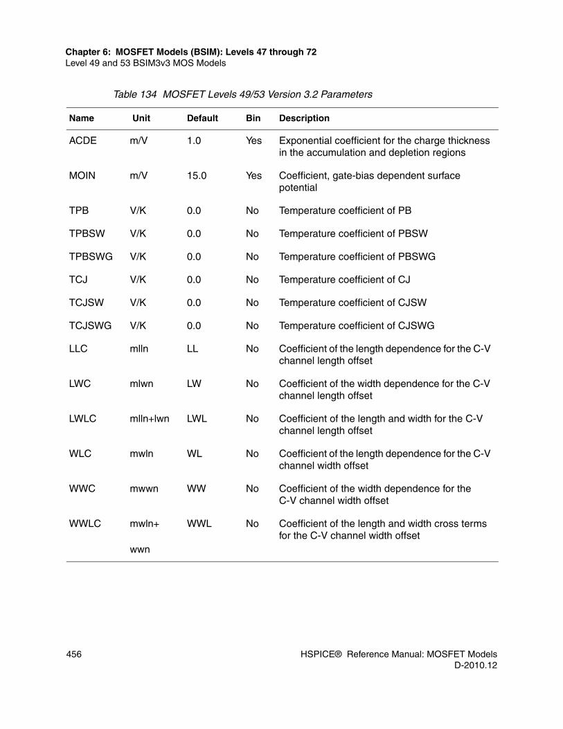
456 HSPICE® Reference Manual: MOSFET ModelsD-2010.12
Chapter 6: MOSFET Models (BSIM): Levels 47 through 72Level 49 and 53 BSIM3v3 MOS Models
ACDE m/V 1.0 Yes Exponential coefficient for the charge thickness in the accumulation and depletion regions
MOIN m/V 15.0 Yes Coefficient, gate-bias dependent surface potential
TPB V/K 0.0 No Temperature coefficient of PB
TPBSW V/K 0.0 No Temperature coefficient of PBSW
TPBSWG V/K 0.0 No Temperature coefficient of PBSWG
TCJ V/K 0.0 No Temperature coefficient of CJ
TCJSW V/K 0.0 No Temperature coefficient of CJSW
TCJSWG V/K 0.0 No Temperature coefficient of CJSWG
LLC mlln LL No Coefficient of the length dependence for the C-V channel length offset
LWC mlwn LW No Coefficient of the width dependence for the C-V channel length offset
LWLC mlln+lwn LWL No Coefficient of the length and width for the C-V channel length offset
WLC mwln WL No Coefficient of the length dependence for the C-V channel width offset
WWC mwwn WW No Coefficient of the width dependence for the C-V channel width offset
WWLC mwln+
wwn
WWL No Coefficient of the length and width cross terms for the C-V channel width offset
Table 134 MOSFET Levels 49/53 Version 3.2 Parameters
Name Unit Default Bin Description

HSPICE® Reference Manual: MOSFET Models 457D-2010.12
Chapter 6: MOSFET Models (BSIM): Levels 47 through 72Level 49 and 53 BSIM3v3 MOS Models
Level 49/53 Notes:1. If you do not specify Cgso, simulation calculates it as follows:
• If you specify a dlc value that is greater than 0.0, then,
cgso=p1=max(0,dlc*cox - cgs1)
Otherwise, cgso=0.6*xj*cox
2. If you do not specify Cgdo, simulation calculates it as follows:
• if you specify a dlc value that is greater than 0.0, then,
cgdo=p2=max(0,dlc*cox - cgd1)
Otherwise cgdo=0.6*xj*cox
3. If you do not specify Cf, simulation calculates it using:
4. If you do not specify Vth0 in the .MODEL statement, simulation calculates it with Vfb=-1, using:
5. If you do not specify K1 and K2, simulation calculates it using:
6. If you do not specify nch, but you specify GAMMA1, then simulation calculates nch from:
7. If you do not specify nch or GAMMA1, then nch defaults to 1.7e17 per cubic meter and simulation calculates GAMMA1 from nch.
8. If you do not specify PHI, simulation calculates it using:
Cf
2ε ox
π----------- 1
47–× 10
Tox------------------+
⎝ ⎠⎜ ⎟⎛ ⎞
log=
Vth0 Vfb φs K1 φs+ +=
K1 GAMMA2 2K2 φs Vbs–+=
K2
GAMMA2 GAMMA1–( ) φs Vbs– φs–( )
2 φs φs Vbm– φs–( ) Vbm+--------------------------------------------------------------------------------------------------------=
nch
GAMMA12COX
2
2qε si-----------------------------------------=

458 HSPICE® Reference Manual: MOSFET ModelsD-2010.12
Chapter 6: MOSFET Models (BSIM): Levels 47 through 72Level 49 and 53 BSIM3v3 MOS Models
9. If you do not specify GAMMA1, simulation calculates it using:
10. If you do not specify GAMMA2, simulation calculates it using:
11. If you do not specify Vbx, simulation calculates it using:
12. The BSIM3 model can calculate Vth in any of three ways:
• Using K1 and K2 values that you specify
• Using GAMMA1, GAMMA2, VBM, and VBX values that you enter in the .MODEL statement
• Using NPEAK, NSUB, XT, and VBM values that you specify
You can enter the U0 model parameter in meters or centimeters. Simulation converts U0 to m2/Vsec as follows: if U0 is greater than 1, it is multiplied by 1e-4. You must enter the NSUB parameter in cm-3 units.
Specify a negative value of VTH0 for the p-channel in the .MODEL statement.
The PSCBE1 and PSCBE2 model parameters determine the impact ionization current, which contributes to the bulk current.
φs 2kBT
q---------
nch
ni-------⎝ ⎠
⎛ ⎞log=
ni 1.45 1010× T
300.15----------------⎝ ⎠
⎛ ⎞ 1.521.5565981
qEg T( )2kBT
------------------–⎝ ⎠⎛ ⎞exp=
Eg T( ) 1.167.02 10
4–× T2
T 1108+----------------------------------–=
GAMMA1
2qε sinch
Cox-------------------------=
GAMMA2
2qε sinsub
Cox---------------------------=
Vbx φs
qnchXt2
2ε si-----------------–=

HSPICE® Reference Manual: MOSFET Models 459D-2010.12
Chapter 6: MOSFET Models (BSIM): Levels 47 through 72Level 49 and 53 BSIM3v3 MOS Models
Parameter Range LimitsSimulation reports either a warning or a fatal error if BSIM3v3 parameters fall outside predefined ranges. These range limitations prevent (or at least warn of) potential numerical problems. Level 53 follows exactly the BSIM3v3 range limit reporting scheme. Level 49 deviates from the BSIM3v3 scheme as noted in the comments column of Table 135.
To control the maximum number of simulation warning messages printing to the output file, use:
.OPTION WARNLIMIT=#
In the preceding .OPTION statement, # is the maximum number of warning messages that simulation reports. The default WARNLIMIT value is 1. In some cases (as noted in Table 135), simulation checks parameters only if you set the PARMAMCHK=1 model parameter.
Table 135 Model Parameter Range Limit, Levels 49/53
Name Limits Comments
TOX Min value=5e-10<=0 Fatal< 10-9 Warn if parmchk=1
BSIM3tox < 5e-10 is automatically reset to min value 5e-10
TOXM <=0 Fatal< 10-9 Warn if parmchk=1
XJ <=0 Fatal
NGATE < 0 Fatal
> 1025 Fatal
<=1018 Fatal if parmchk=1
if >1023 simulation multiplies NGATE
by 10-6 before the other limit checks. Level 49 returns:< 0 Fatal
> 1025 Warn
<=1018 Warn if paramchk==1
NSUB <=0 Fatal
<=1014 Warn if parmchk=1
>=1021 Warn if parmchk=1
Ignores NSUB if k1,k2 are defined

460 HSPICE® Reference Manual: MOSFET ModelsD-2010.12
Chapter 6: MOSFET Models (BSIM): Levels 47 through 72Level 49 and 53 BSIM3v3 MOS Models
NLX < -Leff Fatal< 0 Warn if parmchk=1
NCH <=0 Fatal
<=1015 Warn if parmchk=1
>=1021 Warn if parmchk=1
if >1020 simulation multiplies NCH by
10-6 before the other limit checks.
DVT1W < 0 Fatal < 0 Level 49 reports a warning
DVT0 < 0 Warn if paramchk=1
DVT1 < 0 Fatal < 0 Level 49 reports a warning
ETA0 <=0 Warn if paramchk=1
DSUB < 0 Fatal < 0 Level 49 reports a warning
VBM Ignored if you defined K1 and K2
U0 <=0 Fatal
B1 =-Weff Fatal
B1 + Weff < 10-7 Warn if paramchk=1
VSAT <=0 Fatal
< 103 Warn if paramchk==1
A1 - See A2 conditions on the next line
A2 ■ < 0.01 Warn and reset a2=0.01 if paramchk=1
■ > 1 Warn and reset a2=1,a1=0 if paramchk=1
DELTA < 0 Fatal
RDSW < 0.001 Warn if paramchk=1 and reset rdsw=0
NFACTOR < 0 Warn if paramchk=1
Table 135 Model Parameter Range Limit, Levels 49/53 (Continued)
Name Limits Comments

HSPICE® Reference Manual: MOSFET Models 461D-2010.12
Chapter 6: MOSFET Models (BSIM): Levels 47 through 72Level 49 and 53 BSIM3v3 MOS Models
CDSC < 0 Warn if paramchk=1
CDSCD < 0 Warn if paramchk=1
PCLM <=0 Fatal
PDIBLC1 < 0 Warn if paramchk=1
PDIBLC2 < 0 Warn if paramchk=1
PS < Weff Warn
W0 =-Weff Fatal
w0 + Weff < 10-7 Warn if paramchk==1
DROUT < 0 Fatal if paramchk=1 Level 49 reports a warning
PSCBE2 <=0 warn if paramchk=1
CGS0 < 0 Warn and reset to 0 if paramchk=1
CGD0 < 0 Warn and reset to 0 if paramchk=1
CGB0 < 0 Warn and reset to 0 if paramchk=1
ACDE < 0.4, >1.6 Warn
MOIN < 5.0, >25 Warn
IJTH < 0 Fatal
NOFF < 0.1, >4.0 Warn
Table 136 Element Parameter Range Limit, Levels 49/53
Name Limits Comments
PD < Weff, Warn
Table 135 Model Parameter Range Limit, Levels 49/53 (Continued)
Name Limits Comments

462 HSPICE® Reference Manual: MOSFET ModelsD-2010.12
Chapter 6: MOSFET Models (BSIM): Levels 47 through 72Level 49 and 53 BSIM3v3 MOS Models
For a list of output template parameters in the MOSFET models, and which parameters this model supports, see Table 4 on page 22.
Level 49, 53 EquationsThe effective channel length and width in all model equations are:
Wdrawn=W * WMULT + XWLdrawn=L * LMULT + XL
■ The unprimed Weff is bias-dependent.
■ The primed quantity is bias-independent.
C-V calculations replace dW’ with:
PS < Weff, Warn
Leff < 5.0 x 10⁻⁸ Fatal
Weff < 1.0 x 10⁻⁷ Fatal
LeffCV < 5.0 x 10⁻⁸ Fatal
WeffCV < 1.0 x 10⁻⁷ Fatal
Table 136 Element Parameter Range Limit, Levels 49/53
Leff Ldrawn 2dL–=
Weff Wdrawn 2dW–=
Weff′
Wdrawn 2dW′
–=
dW dW′
dWgVgsteff dWb φs Vbseff– φs–( )+ +=
dW′
Wint
WL
LWLN
-------------WW
WWWN
----------------WWL
LWLN
WWWN
-----------------------------+ + +=
dL Lint
LL
LLLN
------------LW
WLWN
---------------LWL
LLLN
WLWN
---------------------------+ + +=

HSPICE® Reference Manual: MOSFET Models 463D-2010.12
Chapter 6: MOSFET Models (BSIM): Levels 47 through 72Level 49 and 53 BSIM3v3 MOS Models
C-V also replaces dL’ with:
Note: For details of BSIM3 Version 3 equations, see the web site:http://www-device.eecs.berkeley.edu/~bsim3/get.html
.MODEL CARDS NMOS ModelThis is an example of a NMOS model for the Level 49 MOSFET. VTH0 is positive.
.model nch nmos Level=49+ Tnom=27.0+ nch=1.024685E+17 tox=1.00000E-08 xj=1.00000E-07+ lint=3.75860E-08 wint=-2.02101528644562E-07+ vth0=.6094574 k1=.5341038 k2=1.703463E-03 k3=-17.24589+ dvt0=.1767506 dvt1=.5109418 dvt2=-0.05+ nlx=9.979638E-08 w0=1e-6+ k3b=4.139039+ vsat=97662.05 ua=-1.748481E-09 ub=3.178541E-18 uc=1.3623e-10+ rdsw=298.873 u0=307.2991 prwb=-2.24e-4+ a0=.4976366+ keta=-2.195445E-02 a1=.0332883 a2=.9+ voff=-9.623903E-02 nFactor=.8408191 cit=3.994609E-04+ cdsc=1.130797E-04+ cdscb=2.4e-5+ eta0=.0145072 etab=-3.870303E-03+ dsub=.4116711+ pclm=1.813153 pdiblc1=2.003703E-02 pdiblc2=.00129051+ pdiblcb=-1.034e-3+ drout=.4380235 pscbe1=5.752058E+08 pscbe2=7.510319E-05+ pvag=.6370527 prt=68.7 ngate=1.e20 alpha0=1.e-7 beta0=28.4+ prwg=-0.001 ags=1.2+ dvt0w=0.58 dvt1w=5.3e6 dvt2w=-0.0032+ kt1=-.3 kt2=-.03+ at=33000+ ute=-1.5+ ua1=4.31E-09 ub1=7.61E-18 uc1=-2.378e-10
dW′
DWCWLC
LWLN
-------------WWC
WWWN
----------------WWLC
LWLN
WWWN
-----------------------------+ + +=
dL DLCLLC
LLLN
------------LWC
WLWN
---------------LWLC
LLLN
WLWN
---------------------------+ + +=

464 HSPICE® Reference Manual: MOSFET ModelsD-2010.12
Chapter 6: MOSFET Models (BSIM): Levels 47 through 72Level 49 and 53 BSIM3v3 MOS Models
+ kt1l=1e-8+ wr=1 b0=1e-7 b1=1e-7 dwg=5e-8 dwb=2e-8 delta=0.015+ cgdl=1e-10 cgsl=1e-10 cgbo=1e-10 xpart=0.0+ cgdo=0.4e-9 cgso=0.4e-9+ clc=0.1e-6+ cle=0.6+ ckappa=0.6
PMOS ModelExample of a PMOS model for the Level 49 MOSFET. VTH0 is negative.
.model pch PMOS Level=49+ Tnom=27.0+ nch=5.73068E+16 tox=1.00000E-08 xj=1.00000E-07+ lint=8.195860E-08 wint=-1.821562E-07+ vth0=-.86094574 k1=.341038 k2=2.703463E-02 k3=12.24589+ dvt0=.767506 dvt1=.65109418 dvt2=-0.145+ nlx=1.979638E-07 w0=1.1e-6+ k3b=-2.4139039+ vsat=60362.05 ua=1.348481E-09 ub=3.178541E-19 uc=1.1623e-10+ rdsw=498.873 u0=137.2991 prwb=-1.2e-5+ a0=.3276366+ keta=-1.8195445E-02 a1=.0232883 a2=.9+ voff=-6.623903E-02 nFactor=1.0408191 cit=4.994609E-04+ cdsc=1.030797E-3+ cdscb=2.84e-4+ eta0=.0245072 etab=-1.570303E-03+ dsub=.24116711+ pclm=2.6813153 pdiblc1=4.003703E-02 pdiblc2=.00329051 + pdiblcb=-2.e-4+ drout=.1380235 pscbe1=0 pscbe2=1.e-28+ pvag=-.16370527+ prwg=-0.001 ags=1.2+ dvt0w=0.58 dvt1w=5.3e6 dvt2w=-0.0032+ kt1=-.3 kt2=-.03 prt=76.4+ at=33000+ ute=-1.5+ ua1=4.31E-09 ub1=7.61E-18 uc1=-2.378e-10+ kt1l=0+ wr=1 b0=1e-7 b1=1e-7 dwg=5e-8 dwb=2e-8 delta=0.015+ cgdl=1e-10 cgsl=1e-10 cgbo=1e-10 xpart=0.0+ cgdo=0.4e-9 cgso=0.4e-9+ clc=0.1e-6+ cle=0.6+ ckappa=0.6
HSPICE® Reference Manual: MOSFET Models 465D-2010.12
Chapter 6: MOSFET Models (BSIM): Levels 47 through 72Level 54 BSIM4 Model
Level 54 BSIM4 Model
The UC Berkeley BSIM4 model explicitly addresses many issues in modeling sub-0.13 micron CMOS technology and RF high-speed CMOS circuit simulation. The Level 54 model is based on the UC Berkeley BSIM4 MOS model. BSIM4.5 is fully supported in this release. For details, see the BSIM web site:http://www-device.eecs.berkeley.edu/~bsim3/bsim4.html
The following sections discuss these topics:■ Version 4.5 Features■ Other Noise Sources Modeled in v. 4.5■ General Syntax for BSIM4 Model■ Improvements Over BSIM3v3■ Parameter Range Limit for BSIM4 Level 54■ TSMC Diode Model■ BSIM4 Juncap2 Model■ BSIM4 STI/LOD■ Version 4.6 Features■ Version 4.6.2 Features and Updates■ Version 4.6.3 Update■ Level 54 BSIM4 Template Output List
See .OPTION PHD in the HSPICE Reference Manual: Commands and Control Options for the PHD flow that can generally help large case HSPICE DC OP convergence for BSIM4 testcases.
The following sections discuss these topics:■ Version 4.5 Features■ General Syntax for BSIM4 Model■ Improvements Over BSIM3v3■ Parameter Range Limit for BSIM4 Level 54■ TSMC Diode Model■ BSIM4 Juncap2 Model

466 HSPICE® Reference Manual: MOSFET ModelsD-2010.12
Chapter 6: MOSFET Models (BSIM): Levels 47 through 72Level 54 BSIM4 Model
■ BSIM4 STI/LOD■ HSPICE Junction Diode Model and ACM■ Version 4.6 Features■ Version 4.6.1 Features■ Version 4.6.2 Features and Updates■ Version 4.6.3 Update■ Level 54 BSIM4 Template Output List
Version 4.5 FeaturesIn July 2005, Berkeley released BSIM4 Version 4.5, which includes the following features:■ The gate resistance parameters XGW and NGCON are now available as both
model and instance parameters. ■ Four modes are added or enhanced:
• RBODYMOD=2: substrate resistance model that is scalable with channel length, channel width and number fingers
• IGCMOD=2: implements full BSIM4 Vth model into IGC enables accurate predictions of IGC Vbs dependence
• TEMPMOD=2: enhances TEMPMOD so Vth(DITS) and gate tunneling models are functions of nominal temperature and adds the temperature dependence of zero-bias flat-band voltage
• WPEMOD=1: adds a new well-proximity effect model developed by CMC.■ Adds a new mobility model that accounts for Coulomb scattering effect as
well as the channel length dependence of mobility due to heavy halo-doping.
■ Adds additional temperature dependence of model parameters VOFF and VFBSDOFF.
■ A fatal error message is issued when a model parameter VTSS, VTSD, VTSSWS, or VTSSWGD is negative. A warning message was issued previously.

HSPICE® Reference Manual: MOSFET Models 467D-2010.12
Chapter 6: MOSFET Models (BSIM): Levels 47 through 72Level 54 BSIM4 Model
■ A warning message is issued if model parameter CGBO is negative. In which case, CGBO is set to 0.
■ Fixed bugs in BSIM 4.4.
Note: BSIM4 Version 4.5 officially supports instance parameter DELVT0, which is used to represent threshold variations. This parameter has been supported in HSPICE since the 2002.12 version.
Other Noise Sources Modeled in v. 4.5BSIM4 models the thermal noise due to the substrate, electrode gate, and source/drain resistances. Shot noise due to various gate tunneling components is modeled as well.
HSPICE can print out rg, rbps, rbpd, rbpb, rbsb, rbdb, igs, igd, igb noise information. You can add the following noise parameters to the model card.
General Syntax for BSIM4 ModelThe general syntax for including a BSIM4 model element in a netlist is:
Mxxx nd ng ns [nb] mname [L=val] [W=val] [M=val] + [VER_CONTROL=0|1][AD=val] [AS=val] [PD=val] [PS=val] + [RGATEMOD=val] [RBODYMOD=val] [TRNQSMOD=val] + [ACNQSMOD=val] [GEOMOD=val] [RGEOMOD=val] + [NRS=val] [NRD=val] [RBPB=val] [RBPD=val] + [RBPS=val] [RBDB=val] [RBSB=val] [NF=val] + [MIN=val] [RDC=val] [RSC=val] [DELVTO=val] + [MULU0=val] [DELK1=val] [DELNFCT=val]
Output Parameters Turns On...
+ rgatemod=1 The rg noise output
+ rbodymod=1 The rbps, rbpb noise output
+ igbmod=1 The igb noise output
+ igcmod=1 The igs and igd noise output
+ rbsbx0=1 rbsby0=1 rbdbx0=1 rbdby0=1rbodymod=1
The rbsb and rbdb noise output

468 HSPICE® Reference Manual: MOSFET ModelsD-2010.12
Chapter 6: MOSFET Models (BSIM): Levels 47 through 72Level 54 BSIM4 Model
+ [DELTOX=val] [OFF] [IC=Vds, Vgs, Vbs] + [WNFLAG=val] [MULID0=val]
Parameter Description
ACNQSMOD AC small-signal NQS model selector.
AD Drain diffusion area.
AS Source diffusion area.
DELK1 Shift in body bias coefficient (K1).
DELNFCT Shift in subthreshold swing factor (NFACTOR).
DELTOX Shift in gate electrical and physical oxide thickness (TOXE and TOXP). That is, the difference between the electrical and physical gate oxide/insulator thicknesses.
DELVTO (DELVT0)
Shift in the VTH0 zero-bias threshold voltage.
GEOMOD Geometry-dependent parasitics model selector—specifies how the end S/D diffusions connect.
IC Initial guess in the order
L BSIM4 MOSFET channel length in meters.
MIN Whether to minimize the number of drain or source diffusions for even-number fingered device.
mname MOSFET model name reference.
MULU0 Low-field mobility (U0) multiplier.
nb Bulk terminal node name.
nd Drain terminal node name.
NF Number of device fingers.
ng Gate terminal node name.

HSPICE® Reference Manual: MOSFET Models 469D-2010.12
Chapter 6: MOSFET Models (BSIM): Levels 47 through 72Level 54 BSIM4 Model
NRD Number of drain diffusion squares.
NRS Number of source diffusion squares.
ns Source terminal node name.
OFF Sets the initial condition to OFF in DC analysis.
PD Perimeter of the drain junction:■ If PERMOD=0, it excludes the gate edge.■ Otherwise, it includes the gate edge.
PS Perimeter of the source junction:■ If PERMOD=0, it excludes the gate edge.■ Otherwise, it includes the gate edge.
RBDB Resistance connected between dbNode and bNode.
RBODYMOD Substrate resistance network model selector.
RBPB Resistance connected between bNodePrime and bNode.
RBPD Resistance connected between bNodePrime and dbNode.
RBPS Resistance connected between bNodePrime and sbNode.
RBSB Resistance connected between sbNode and bNode.
RDC Drain contact resistance for per-finger device.
RGATEMOD Gate resistance model selector.
RGEOMOD Source/drain diffusion resistance and contact model selector—specifies the end S/D contact type: point wide or merged) and how to compute the S/D parasitics resistance.
RSC Source contact resistance for per-finger device.
TRNQSMOD Transient NQS model selector.
W BSIM4 MOSFET channel width in meters.
Parameter Description

470 HSPICE® Reference Manual: MOSFET ModelsD-2010.12
Chapter 6: MOSFET Models (BSIM): Levels 47 through 72Level 54 BSIM4 Model
Improvements Over BSIM3v3BSIM4 includes the following major improvements and additions over BSIM3v3:■ An accurate new model of the intrinsic input resistance (Rii) for both RF,
high-frequency analog, and high-speed digital applications ■ A flexible substrate resistance network for RF modeling■ A new accurate channel thermal noise model, and a noise partition model
for the induced gate noise■ A non-quasi-static (NQS) model consistent with the Rii-based RF model,
and a consistent AC model that accounts for the NQS effect in both transconductances and capacitances
■ An accurate gate direct tunneling model■ A comprehensive and versatile geometry-dependent parasitics model for
source/drain connections and multi-finger devices■ An improved model for steep vertical retrograde doping profiles■ A better model for pocket-implanted devices in Vth, the bulk charge effect
model, and Rout■ An asymmetrical and bias-dependent source/drain resistance, either
internal or external to the intrinsic MOSFET■ Accepts either the electrical or physical gate oxide thickness as the model
input in a physically accurate manner■ A quantum mechanical charge-layer-thickness model for both IV and CV■ A more accurate mobility model for predictive modeling
WNFLAG Turn on to select bin model based on width per NF for multi-finger devices.
MULID0 Scaling factor of drain current, the default is 1.0.
VER_CONTROL ■ VER_CONTROL=0: (Default) Version control is off■ VER_CONTROL=1: Version control is on; the simulation will abort
for non-supported version
Parameter Description
HSPICE® Reference Manual: MOSFET Models 471D-2010.12
Chapter 6: MOSFET Models (BSIM): Levels 47 through 72Level 54 BSIM4 Model
■ A gate-induced drain leakage (GIDL) current model, not available in earlier BSIM models
■ An improved unified flicker (1/f) noise model, which is smooth over all bias regions, and which considers the bulk charge effect
■ Different diode IV and CV characteristics for the source and drain junctions■ A junction diode breakdown with or without current limiting■ A dielectric constant of the gate dielectric as a model parameter■ .OPTION LIST now prints the total capacitances, instead of just the
intrinsic capacitances for the BSIM4 (Level 54) MOSFET model
BSIM4.2.1 has the following improvements over BSIM4.2.0:■ A new GISL (Gate Induced Source Leakage) current component
corresponds to the same current at the drain side (GIDL).■ The warning limits for effective channel length, channel width, and gate
oxide thickness have been reduced to avoid unnecessary warnings if you use BSIM4 aggressively, beyond the desired model card application ranges.
■ The DELTOX parameter in the MOS active element (M) models the relative variation on the trans conductance (oxide thickness) of the MOS in Monte Carlo analysis.
■ .OPTION LIST can now print an element summary for the MOSFET Level=54 model
Parameter Range Limit for BSIM4 Level 54Simulation reports either a warning or a fatal error if BSIM3v3 parameters fall outside predefined ranges. These range limitations prevent (or at least warn of) potential numerical problems.
To control the maximum number of simulation warning messages printing to the output file, use:
.OPTION WARNLIMIT=#
In the preceding .OPTION statement, # is the maximum number of warning messages that simulation reports. The default WARNLIMIT value is 1. In some

472 HSPICE® Reference Manual: MOSFET ModelsD-2010.12
Chapter 6: MOSFET Models (BSIM): Levels 47 through 72Level 54 BSIM4 Model
cases (as noted in Table 137 below), simulation checks parameters only if you set the PARMAMCHK=1 model parameter.
Table 137 Model Parameter Range Limit, Level 54
Parameter Limits Comment
toxref <= 0 fatal
lpe0 < -leff, fatal
lintnoi > leff/2, fatal if (version>=4.39999)
lpeb < -leff, fatal
phin < -0.4 fatal if (version>=4.4 phin <=0 fatal
ndep <= 0 fatal
nsub <= 0 fatal
ngate < 0,> 1.0e25 fatal
xj <= 0 fatal
dvt1 < 0 fatal
dvt1w < 0 fatal
w0 w0=-weff fatal
dsub < 0 fatal
b1 b1=-weff fatal
delta < 0 fatal
pclm <= 0 fatal
drout < 0 fatal
pscbe2 <= 0 fatal
nf < 1 fatal
ngcon < 1 fatal If ngcon !=1,2 warn and set 1

HSPICE® Reference Manual: MOSFET Models 473D-2010.12
Chapter 6: MOSFET Models (BSIM): Levels 47 through 72Level 54 BSIM4 Model
gbmin < 1.0e-20 warn
noff =0 warn and set 1; < 0.1 warn
if (version < 4.2999||stiMod=2) noff > 4 warn
voffcv < -0.5 warn if (version<4.2999||stiMod=2) voffcv > 0.5 warn
clc < 0 fatal
moin < 5.0, > 25 warn
acde < 0.1, > 1.6 warn if (version < 4.29999) acde<0.4 warn
ckappas < 0.02 warn and set 0.02 if (version >= 4.299999 &&stiMod != 2) || version < 4.299999)
ckappad < 0.02 warn and set 0.02 if (version >= 4.299999 &&stiMod != 2) || version < 4.299999)
if paramchk=1 the following parameter limit range is added
leff <= 1e-9 warn
leffcv <= 1e-9 warn
weff <= 1e-9 warn
weffcv <= 1e-9 warn
toxe Toxe + Deltox < 1e-10 warn
toxp Toxp + Deltox< 1e-10 warn
toxm < 1e-10 warn
ndep <= 1e12, >= 1e21 warn
nsub <= 1e14, >= 1e21 warn
Table 137 Model Parameter Range Limit, Level 54
Parameter Limits Comment

474 HSPICE® Reference Manual: MOSFET ModelsD-2010.12
Chapter 6: MOSFET Models (BSIM): Levels 47 through 72Level 54 BSIM4 Model
ngate 0 <ngate <= 1e18 warn
dvt0 < 0 warn
w0 w0+weff< 1e-7 warn if (version> =4.39999) w0+weff < 1e-9 warn
nfactor < 0 warn
cdsc < 0 warn
cdscd < 0 warn
eta0 < 0 warn
b1 b1+weff< 1e-7 warn if (version>=4.39999) b1+weff<1e-9 warn
a2 < 0.01 warn, set 0.01; >1 .0 warn, set 1 and a1 set 0
- If the total calculated A2 (including binnings) is smaller than 0.01, then it is set to 0.01.
- If the total A2 is larger than 1, it is set to 1.
prwg < 0 warn, set 0
rdsw < 0 warn, set 0
rds0 < 0 warn, set 0
rdswmin < 0 warn, set 0
vsattemp <1e3 warn
lambda > 1e-9 warn if (version>=4.3)
vtl < 6e4 warn if (version>=4.3)
xn < 3 if (version>= 4.3)
lc < 0 if (version>= 4.3)
Table 137 Model Parameter Range Limit, Level 54
Parameter Limits Comment

HSPICE® Reference Manual: MOSFET Models 475D-2010.12
Chapter 6: MOSFET Models (BSIM): Levels 47 through 72Level 54 BSIM4 Model
prout < 0 fatal
pdits < 0 fatal
pditsl < 0 fatal
pdibl1 < 0 warn
pdibl2 < 0 warn
lodk2 <= 0 warn if (version>= 4.4)
lodeta0 <= 0 warn if (version>= 4.4)
nigbinv <= 0 fatal
nigbacc <= 0 fatal
nigc <= 0 fatal
poxedge <= 0 fatal
pigcd <= 0 fatal
rshg <= 0 warn if (version >= 4.299999 && stiMod != 2)
xrcrg1 <=0 warn if (version >= 4.299999 && stiMod != 2)
sl < 1e-7 warn; < 0 fatal
sw < 1e-7 warn; < 0 fatal
sa < 0 fatal
sb < 0 fatal
sd < 0 fatal If nf>1
sa0 <= 0 fatal
sb0 <= 0 fatal
Table 137 Model Parameter Range Limit, Level 54
Parameter Limits Comment

476 HSPICE® Reference Manual: MOSFET ModelsD-2010.12
Chapter 6: MOSFET Models (BSIM): Levels 47 through 72Level 54 BSIM4 Model
wlod < 0 fatal
kvsat < -1.0, > 1.0 fatal
lodk2 <= 0
lodeta0 <= 0
nf >1 fatal if (stiMod == 2)
cgdo < 0 warn
cgso < 0 warn
cgbo < 0 warn if (version >4.4999)
tnoia < 0 warn
tnob < 0 warn
rnoia < 0 warn
rnoib < 0 warn
ntnoi < 0 warn
Njs < 0 warn
Njd < 0 warn
Njts < 0 warn
Njtssw < 0 warn
Njtsswg < 0 warn
Njtsd < 0 warn
Njtsswd < 0 warn
Njtsswgd < 0 warn
Table 137 Model Parameter Range Limit, Level 54
Parameter Limits Comment
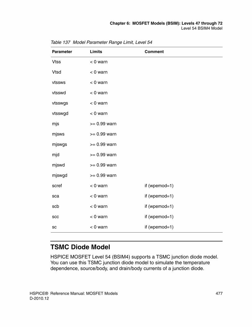
HSPICE® Reference Manual: MOSFET Models 477D-2010.12
Chapter 6: MOSFET Models (BSIM): Levels 47 through 72Level 54 BSIM4 Model
TSMC Diode ModelHSPICE MOSFET Level 54 (BSIM4) supports a TSMC junction diode model. You can use this TSMC junction diode model to simulate the temperature dependence, source/body, and drain/body currents of a junction diode.
Vtss < 0 warn
Vtsd < 0 warn
vtssws < 0 warn
vtsswd < 0 warn
vtsswgs < 0 warn
vtsswgd < 0 warn
mjs >= 0.99 warn
mjsws >= 0.99 warn
mjswgs >= 0.99 warn
mjd >= 0.99 warn
mjswd >= 0.99 warn
mjswgd >= 0.99 warn
scref < 0 warn if (wpemod=1)
sca < 0 warn if (wpemod=1)
scb < 0 warn if (wpemod=1)
scc < 0 warn if (wpemod=1)
sc < 0 warn if (wpemod=1)
Table 137 Model Parameter Range Limit, Level 54
Parameter Limits Comment
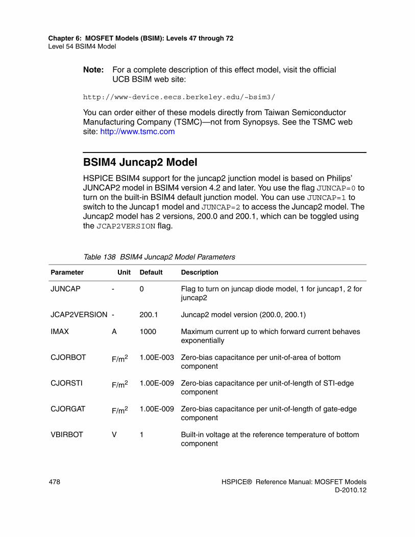
478 HSPICE® Reference Manual: MOSFET ModelsD-2010.12
Chapter 6: MOSFET Models (BSIM): Levels 47 through 72Level 54 BSIM4 Model
Note: For a complete description of this effect model, visit the official UCB BSIM web site:
http://www-device.eecs.berkeley.edu/~bsim3/
You can order either of these models directly from Taiwan Semiconductor Manufacturing Company (TSMC)—not from Synopsys. See the TSMC web site: http://www.tsmc.com
BSIM4 Juncap2 ModelHSPICE BSIM4 support for the juncap2 junction model is based on Philips’ JUNCAP2 model in BSIM4 version 4.2 and later. You use the flag JUNCAP=0 to turn on the built-in BSIM4 default junction model. You can use JUNCAP=1 to switch to the Juncap1 model and JUNCAP=2 to access the Juncap2 model. The Juncap2 model has 2 versions, 200.0 and 200.1, which can be toggled using the JCAP2VERSION flag.
Table 138 BSIM4 Juncap2 Model Parameters
Parameter Unit Default Description
JUNCAP - 0 Flag to turn on juncap diode model, 1 for juncap1, 2 for juncap2
JCAP2VERSION - 200.1 Juncap2 model version (200.0, 200.1)
IMAX A 1000 Maximum current up to which forward current behaves exponentially
CJORBOT F/m2 1.00E-003 Zero-bias capacitance per unit-of-area of bottom component
CJORSTI F/m2 1.00E-009 Zero-bias capacitance per unit-of-length of STI-edge component
CJORGAT F/m2 1.00E-009 Zero-bias capacitance per unit-of-length of gate-edge component
VBIRBOT V 1 Built-in voltage at the reference temperature of bottom component

HSPICE® Reference Manual: MOSFET Models 479D-2010.12
Chapter 6: MOSFET Models (BSIM): Levels 47 through 72Level 54 BSIM4 Model
VBIRSTI V 1 Built-in voltage at the reference temperature of TI-edge component
VBIRGAT V 1 Built-in voltage at the reference temperature of gate-edge component
PBOT - 0.5 Grading coefficient of bottom component
PSTI - 0.5 Grading coefficient of STI-edge component
PGAT - 0.5 Grading coefficient of gate-edge component
PHIGBOT V 1.16 Zero-temperature bandgap voltage of bottom component
PHIGSTI V 1.16 Zero-temperature bandgap voltage of STI-edge component
PHIGGAT V 1.16 Zero-temperature bandgap voltage of gate-edge component
IDSATRBOT A/m2 1.00E-012 Saturation current density at the reference temperature of bottom component
IDSATRSTI A/m 1.00E-018 Saturation current density at the reference temperature of STI-edge component
IDSATRGAT Am 1.00E-018 SATURATION current density at the reference temperature of gate-edge component
CSRHBOT A/m2 1.00E+002 Shockley-Read-Hall prefactor of bottom component
CSRHSTI A/m2 1.00E-004 Shockley-Read-Hall prefactor of STI-edge component
CSRHGAT A/m2 1.00E-004 Shockley-Read-Hall prefactor of gate-edge component
XJUNSTI m 1.00E-007 Junction depth of STI-edge component
XJUNGAT m 1.00E-007 junction depth of gate-edge component
CTATBOT A/m3 1.00E+002 Trap-assisted tunneling prefactor of bottom component
Table 138 BSIM4 Juncap2 Model Parameters (Continued)
Parameter Unit Default Description

480 HSPICE® Reference Manual: MOSFET ModelsD-2010.12
Chapter 6: MOSFET Models (BSIM): Levels 47 through 72Level 54 BSIM4 Model
CTATSTI A/m2 1.00E-004 Trap-assisted tunneling prefactor of STI-edge component
CTATGAT A/m2 1.00E-004 Trap-assisted tunneling prefactor of gate-edge component
MEFFTATBOT - 0.25 Effective mass (in units of m0) for trap-assisted tunneling of bottom component
MEFFTATSTI - 0.25 Effective mass (in units of m0) for trap-assisted tunneling of STI-edge component
MEFFTATGAT - 0.25 Effective mass (in units of m0) for trap-assisted tunneling of gate-edge component
CBBTBOT AV-3 1.00E-012 Band-to-band tunneling prefactor of bottom component
CBBTSTI AV-3m 1.00E-018 Band-to-band tunneling prefactor of STI-edge component
CBBTGAT AV-3m 1.00E-018 Band-to-band tunneling prefactor of gate-edge component
FBBTRBOT V/m 1.00E+009 Normalization field at the reference temperature for band-to-band tunneling of bottom component
FBBTRSTI V/m 1.00E+009 Normalization field at the reference temperature for band-to-band tunneling of STI-edge component
FBBTRGAT V/m 1.00E+009 Normalization field at the reference temperature for band-to-band tunneling of gate-edge component
STFBBTBOT 1/K -1.00E-003 temperature scaling parameter for band-to-band tunneling of bottom component
STFBBTSTI 1/K -1.00E-003 temperature scaling parameter for band-to-band tunneling of STI-edge component
STFBBTGAT 1/K -1.00E-003 temperature scaling parameter for band-to-band tunneling of gate-edge component
Table 138 BSIM4 Juncap2 Model Parameters (Continued)
Parameter Unit Default Description

HSPICE® Reference Manual: MOSFET Models 481D-2010.12
Chapter 6: MOSFET Models (BSIM): Levels 47 through 72Level 54 BSIM4 Model
BSIM4 STI/LODHSPICE BSIM4 supports the full STI (Shallow Trench Isolation) or LOD (Length of Oxide Definition) induced mechanical stress-effect model (for version 4.3 or later), which was first released in the UCB BSIM4.3.0 model version. HSPICE BSIM4 turns on the simulation of this effect when the following conditions (consistent with those of the UCB BSIM4 model) are satisfied:
if (VERSION >=4.3) {if ((SA > 0 and SB > 0 and NF==1) or ( SA > 0 and SB > 0 and ( NF >1 and SD > 0 ))){ UCB's STI/LOD model is turned on}}
If VERSION>=4.3, the STI model is not dependent on STIMOD=0 or 1. In this case, the STI model is applied to the model similar to the UCB STI model (see Table 139). When parameter values that satisfy SA>0, SB>0, NF>1, and SD=0 are given in model cards, no evaluation of such effect is performed.
VBRBOT V 10 breakdown voltage of bottom component
VBRSTI V 10 breakdown voltage of STI-edge component
VBRGAT V 10 breakdown voltage of gate-edge component
PBRBOT V 4 breakdown onset tuning parameter of bottom component
PBRSTI V 4 breakdown onset tuning parameter of STI-edge component
PBRGA V 4 breakdown onset tuning parameter of gate-edge component
Table 138 BSIM4 Juncap2 Model Parameters (Continued)
Parameter Unit Default Description

482 HSPICE® Reference Manual: MOSFET ModelsD-2010.12
Chapter 6: MOSFET Models (BSIM): Levels 47 through 72Level 54 BSIM4 Model
Table 139 Supported HSPICE BSIM4 STI/LOD Parameters
Parameter Unit Default Bin? Description
SA (instance parameter)
0.0 Distance between S/D diffusion edge to poly gate edge from one side. If not given, or, if (<=0), the stress effect is turned off.
SB (instance parameter)
0.0 Distance between S/D diffusion edge to poly gate edge from the other side. If not given or, if (<=0), the stress effect is turned off
SD (instance
parameter)
0.0 Distance between neighboring fingers. For NF >1,If not given or (<=0), stress effect is turned off
STIMOD (Also instance parameter)
0.0 (V < 4.3)1.0 (V >=4.3)
STI model selector, which gives priority to the instance parameter. ■ 0: No STI effect. ■ 1: UCB's STI model■ 2: TSMC's STI model
SAREF M 1e-06 No Reference distance for SA, >0.0
SBREF M 1e-06 No Reference distance for SB, >0.0
WLOD M 0.0 No Width parameter for stress effect
KU0 M 0.0 No Mobility degradation/enhancement coefficient for stress effect
KVSAT M 0.0 No Saturation velocity degradation/enhancement
parameter for stress effect. 1.0<=kvsat<=1.0
TKU0 0.0 No Temperature coefficient of KU0
LKU0 0.0 No Length dependence of KU0
WKU0 0.0 No Width dependence of KU0
LLODKU0 0.0 No Length parameter for U0 stress effect, >0

HSPICE® Reference Manual: MOSFET Models 483D-2010.12
Chapter 6: MOSFET Models (BSIM): Levels 47 through 72Level 54 BSIM4 Model
LMLT and WMLT in BSIM4You can use LMLT and WMLT to shrink the length and width in memory design. The LMLT and WMLT parameters are unitless, and are used to scale (usually scale down) MOSFET drawn length and width (specified in BSIM4 MOSFET instance lines), respectively. This makes memory design and netlist creation quite convenient because most (if not all) memory circuits use the smallest feature sizes as the process capability improves, even within the same generation of CMOS technology.
The shrunken device length and width will then be further offset (by XL and XW, respectively) to the actual device size in lithography and etching process steps, and finally to the electrical size as a result of subsequent ion implementation and annealing steps.
WLODKU0 0.0 No Width parameter for U0 stress effect, >0
KVTH0 V*m 0.0 No Threshold shift parameter for stress effect
WKVTH0 0.0 No Width dependence of KVTH0
PKVTH0 0.0 No Cross-term dependence of KVTH0
LLODVTH 0.0 No Length parameter for Vth stress effect, >0
WLODVTH 0.0 No Width parameter for Vth stress effect, >0
STK2 0.0 No K2 shift factor related to VTh0 change
LODK2 m 1.0 No K2 shift modification factor for stress effect, >0
STETA0 0.0 No ETA0 shift factor related to VTH0 change
LODETA0 M 1.0 No ETA0 shift modification factor for stress effect, >0
Table 139 Supported HSPICE BSIM4 STI/LOD Parameters
Parameter Unit Default Bin? Description

484 HSPICE® Reference Manual: MOSFET ModelsD-2010.12
Chapter 6: MOSFET Models (BSIM): Levels 47 through 72Level 54 BSIM4 Model
Both LMLT and WMLT must be greater than 0; if not, simulation resets them to 1.0 (default) and issues a warning message.
To use these two parameters, add them in the model cards, without any other modifications. For example:
.model nmos nmos+ level=54 lmlt=0.85 wmlt=0.9
■ The drawn channel length (L) is multiplied by LMLT.■ The drawn channel width (W) is multiplied by WMLT,
BSIM4 evaluates the effective length and width, Leff and Weff, as:
Leff=Lnew - 2.0 * dLWeff=Wnew - 2.0 * dW
Lnew and Wnew are evaluated as:
Lnew=L + XLWnew=W + XW
dL and dW are evaluated with Lnew and Wnew:
T0=pow(Lnew, LLN)T1=pow(Wnew, LWN)dL=LINT + LL/T0 + LW / T1 + LWL / (T0*T1)T2=pow(Lnew, WLN)T3=pow(Wnew, WWN)dw=WINT + WL / T2 + WW / T3 + WWL / (T2*T3)
Similarly, the preceding equations determine the Ldlc, Ldlcig, LeffCV, Wdwc, Wdwcig, WeffCV, WeffCJ, grgeltd, and Wnew model variables and quantities.
When multiplied by the LMLT and WMLT parameters, Leff and Weff become:
Leff=Lnew' - 2.0 * dLWeff=Wnew' - 2.0 * dL
Lnew' and Wnew' are evaluated as:
Name (Alias) Default Description
LMLT 1.0 Channel length shrinking factor
WMLT 1.0 Device width shrinking factor

HSPICE® Reference Manual: MOSFET Models 485D-2010.12
Chapter 6: MOSFET Models (BSIM): Levels 47 through 72Level 54 BSIM4 Model
Lnew'=L * LMLT + XLWnew'=W * WMLT + XW
Similarly, dL, dW, Ldlc, Ldlcig, LeffCV, Wdwc, Wdwcig, WeffCV, WeffCJ, and grgeltd are all evaluated from Lnew' and Wnew'.
HSPICE Junction Diode Model and ACMBSIM4 now supports Area Calculation Method (ACM) similar to BSIM3v3 for the following models and corresponding ACM values:■ For the HSPICE junction model, specify ACM=0,1,2, or 3.■ For the Berkeley BSIM4 junction model, specify ACM=10,11,12, or 13.
For the junction current, junction capacitance, and parasitic resistance equations corresponding to ACM=0,1,2,3 see MOSFET Diode Models on page 701.
Table 140 MOSFET Level 54 Parameters
Parameter Description
nf Number of device fingers
min Whether to minimize the number of drain or source diffusions for even-number fingered device
rbdb Resistance connected between the internal drain-side body node and the external body node
rbsb Resistance connected between the internal source-side body node and the external body node
rbpb Resistance connected between the internal reference body node and the external body node
rbps Resistance connected between the internal reference body node and the internal drain-side body node
rbpd Resistance connected between the internal reference body node and the internal source-side body node
trnqsmod Transient NQS model selector

486 HSPICE® Reference Manual: MOSFET ModelsD-2010.12
Chapter 6: MOSFET Models (BSIM): Levels 47 through 72Level 54 BSIM4 Model
MOSFET Level 54 uses the generic MOSFET model parameters described in Chapter 2, Common MOSFET Model Parameters. It also uses the parameters described in this section, which apply only to MOSFET Level 54.
The simulation calculates Rd and Rs as follows:
Rd(TEMP)=Rd(TNOM) * (1 + TRD * (TEMP - TNOM))Rs(TEMP)=Rs(TNOM) * (1 + TRS * (TEMP - TNOM))
acnqsmod AC small-signal NQS model selector
rbodymod Substrate resistance network model selector
rgatemod Gate resistance model selector
geomod Geometry-dependent parasitics model selector
rgeomod Source/Drain diffusion resistance and contact model selector
Table 141 Instance Parameters, Level 54
Parameter Unit Default Description
RDC ohm 0.0 Drain contact resistance for the per-finger device
RSC ohm 0.0 Source contact resistance for the per-finger device
DELVTO(DELVT0)
V 0.0 Shift in the zero-bias threshold voltage (VTH0)
MULU0 1.0 Low-field mobility (U0) multiplier
DELK1 V1/2 Shift in the body bias coefficient (K1)
DELNFCT 0.0 Shift in subthreshold swing factor (NFACTOR)
Table 140 MOSFET Level 54 Parameters
Parameter Description

HSPICE® Reference Manual: MOSFET Models 487D-2010.12
Chapter 6: MOSFET Models (BSIM): Levels 47 through 72Level 54 BSIM4 Model
Table 142 Model Selectors/Controllers, Level 54
Parameter Default Binnable Description
VERSION 4.5 NA Model version number
BINUNIT 1 NA Binning unit selector
PARAMCHK 1 NA Switch for the parameter check
MOBMOD 1 NA Mobility model selector
RDSMOD 0 NA Bias-dependent source/drain resistance model selector
IGCMOD 0 NA Gate-to-channel tunneling current model selector
IGBMOD 0 NA Gate-to-substrate tunneling current model selector
CAPMOD 2 NA Capacitance model selector
RGATEMOD 0 (no gate resistance)
Gate resistance model selector
RBODYMOD 0 (network off)
NA Substrate resistance network model selector
TRNQSMOD 0 NA Transient NQS model selector
ACNQSMOD 0 NA AC small-signal NQS model selector
FNOIMOD 1 NA Flicker noise model selector
TNOIMOD 0 NA Thermal noise model selector
DIOMOD 1 NA Source/drain junction diode IV model selector
TEMPMOD 0 NA Temperature mode selector

488 HSPICE® Reference Manual: MOSFET ModelsD-2010.12
Chapter 6: MOSFET Models (BSIM): Levels 47 through 72Level 54 BSIM4 Model
PERMOD 1 NA PS/PD includes/excludes the gate-edge perimeter
GEOMOD 0 (isolated)
NA Geometry-dependent parasitics model selector
RGEOMOD 0(no S/D diffusion resistance)
NA Source/drain diffusion resistance and contact model selector
WPEMOD 0 NA Flag for WPE model (WPEMOD=1 to activate this model)
Table 143 Level 54 Process Parameters, Level 54
Parameter Default Binnable Description
EPSROX 3.9 (SiO2) No Gate dielectric constant relative to vacuum
TOXE 3.0e-9m No Electrical gate equivalent oxide thickness
TOXP TOXE No Physical gate equivalent oxide thickness
TOXM TOXE No Tox at which simulation extracts parameters
DTOX 0.0m No Defined as (TOXE-TOXP)
XJ 1.5e-7m Yes S/D junction depth
GAMMA1 ( 1 in equation)
calculated
(V1/2)
Yes Body-effect coefficient near the surface
GAMMA2 ( 2 in equation)
calculated
(V1/2)
Yes Body-effect coefficient in the bulk
NDEP 1.7e17cm-3 Yes Channel doping concentration at the depletion edge for the zero body bias
Table 142 Model Selectors/Controllers, Level 54
Parameter Default Binnable Description
γ
γ

HSPICE® Reference Manual: MOSFET Models 489D-2010.12
Chapter 6: MOSFET Models (BSIM): Levels 47 through 72Level 54 BSIM4 Model
NSUB 6.0e16cm-3 Yes Substrate doping concentration
NGATE 0.0cm-3 Yes Poly Si gate doping concentration
NSD 1.0e20cm-3 Yes Source/drain doping concentration
VBX calculated (v) No Vbs at which the depletion region width equals XT
XT 1.55e-7m Yes Doping depth
RSH 0.0ohm/square No Source/drain sheet resistance
RSHG 0.1ohm/square No Gate electrode sheet resistance
Table 144 Basic Model Parameters, Level 54
Parameter Default Binnable Description
A0 1.0 Yes Coefficient of the channel-length dependence of the bulk charge effect
A1 0.0V-1 Yes First non-saturation effect parameter
A2 1.0 Yes Second non-saturation factor
AGS 0.0V-1 Yes Coefficient of the Vgs dependence of the bulk charge effect
B0 0.0m Yes Bulk charge effect coefficient for the channel width
B1 0.0m Yes Bulk charge effect width offset
CDSC 2.4e-4F/m2 Yes Coupling capacitance between the source/drain and the channel
CDSCB 0.0F/(Vm2) Yes Body-bias sensitivity of CDSC
Table 143 Level 54 Process Parameters, Level 54 (Continued)
Parameter Default Binnable Description

490 HSPICE® Reference Manual: MOSFET ModelsD-2010.12
Chapter 6: MOSFET Models (BSIM): Levels 47 through 72Level 54 BSIM4 Model
CDSCD 0.0(F/Vm2) Yes Drain-bias sensitivity of DCSC
CIT 0.0F/m2 Yes Interface trap capacitance
DELTA (in equation)
0.01V Yes Parameter for DC Vdseff
DROUT 0.56 Yes Channel-length dependence of the DIBL effect on Rout
DSUB DROUT Yes DIBL coefficient exponent in the subthreshold region
DVT0 2.2 Yes First coefficient of the short-channel effect on Vth
DVT0W 0.0 Yes First coefficient of the narrow width effect on Vth for a small channel length
DVT1 0.53 Yes Second coefficient of the short-channel effect on Vth
DVT1W 5.3e6m-1 Yes Second coefficient of the narrow width effect on Vth for a small channel length
DVT2 -0.032V-1 Yes Body-bias coefficient of the short-channel effect on Vth
DVT2W -0.032V-1 Yes Body-bias coefficient of narrow width effect for small channel length
DVTP0 0.0m Yes First coefficient of the drain-induced Vth shift due to long-channel pocket devices
DVTP1 0.0V-1 Yes First coefficient of the drain-induced Vth shift due to long-channel pocket devices
DWB 0.0m/V1/2 Yes Coefficient of the body bias dependence of the Weff bias dependence
Table 144 Basic Model Parameters, Level 54 (Continued)
Parameter Default Binnable Description
δ

HSPICE® Reference Manual: MOSFET Models 491D-2010.12
Chapter 6: MOSFET Models (BSIM): Levels 47 through 72Level 54 BSIM4 Model
DWG 0.0m/V Yes Coefficient of gate bias dependence of Weff
ETA0 0.08 Yes DIBL coefficient in the subthreshold region
ETAB -0.07V-1 Yes Body-bias coefficient for the DIBL effect for the subthreshold
EU 1.67 (NMOS); 1.0 (PMOS)
No Exponent for the mobility degradation of MOBMOD=2
FPROUT 0.0V/m0.5 Yes Effect of the pocket implant on Rout degradation
K1 0.5V1/2 Yes First-order body bias coefficient
K2 0.0 Yes Second-order body bias coefficient
K3 80.0 Yes Narrow width coefficient
K3B 0.0V-1 Yes Body effect coefficient of K3
KETA -0.047V-1 Yes Body-bias coefficient of the bulk charge effect
LINT 0.0m No Channel-length offset parameter
LP 1e-8(m) Yes Mobility channel length degradation of MOBMOD=2
LPE0 1.74e-7m Yes Lateral non-uniform doping parameter
LPEB 0.0m Yes Lateral non-uniform doping effect on K1
MINV 0.0 Yes Vgsteff fitting parameter for the moderate inversion condition
NFACTOR 1.0 Yes Subthreshold swing factor
PCLM 1.3 Yes Channel-length modulation parameter
Table 144 Basic Model Parameters, Level 54 (Continued)
Parameter Default Binnable Description

492 HSPICE® Reference Manual: MOSFET ModelsD-2010.12
Chapter 6: MOSFET Models (BSIM): Levels 47 through 72Level 54 BSIM4 Model
PDIBLC1 0.39 Yes Parameter for the DIBL effect on Rout
PDIBLC2 0.0086 Yes Parameter for the DIBL effect on Rout
PDIBLCB 0.0V-1 Yes Body bias coefficient of the DIBL effect on Rout
PDITS 0.0V-1 Yes Impact of the drain-induced Vth shift on Rout
PDITSD 0.0V-1 Yes Vds dependence of the drain-induced Vthshift for Rout
PDITSL 0.0m-1 No Channel-length dependence of the drain-induced Vth shift for Rout
PHIN 0.0V Yes Non-uniform vertical doping effect on the surface potential
PSCBE1 4.24e8V/m Yes First substrate current induced body-effect parameter
PSCBE2 1.0e-5m/V Yes Second substrate current induced body-effect parameter
PVAG 0.0 Yes Gate-bias dependence of Early voltage
U0 0.067m2/(Vs) (NMOS); 0.025
m2/(Vs) (PMOS)
Yes Low-field mobility
UA 1.0e-9m/V for MOBMOD=0 and 1; 1.0e-15m/V for MOBMOD=2
Yes Coefficient of the first-order mobility degradation due to the vertical field
UB 1.0e-19m2/V2 Yes Coefficient of the second-order mobility degradation due to the vertical field
Table 144 Basic Model Parameters, Level 54 (Continued)
Parameter Default Binnable Description

HSPICE® Reference Manual: MOSFET Models 493D-2010.12
Chapter 6: MOSFET Models (BSIM): Levels 47 through 72Level 54 BSIM4 Model
UC -0.0465V-1 for MOB-MOD=1;
-0.0465e-9 m/V2 for MOBMOD=0 and 2
Yes Coefficient of the mobility degradation due to the body-bias effect
UD 1e14(1/m2) Yes Mobility coulomb scattering coefficient
UP 0(1/m2) Yes Mobility channel length coefficient
VBM -3.0V Yes Maximum applied body bias in the VTH0 calculation
VFB -1.0V Yes Flat-band voltage (PHIN)
VOFF -0.08V Yes Offset voltage in subthreshold region for large W and L
VOFFL 0.0mV No Channel-length dependence of VOFF
VSAT 8.0e4m/s Yes Saturation velocity
VTH0 orVTHO
0.7V (NMOS)-0.7V (PMOS)
Yes Long-channel threshold voltage at Vbs=0
W0 2.5e-6m Yes Narrow width parameter
WINT 0.0m No Channel-width offset parameter
Table 145 Parameters for Asymmetric and Bias-Dependent Rds Model, Level 54
Parameter Default Binnable Description
PRWB 0.0V-0.5 Yes Body-bias dependence of the LDD resistance
PRWG 1.0V-1 Yes Gate-bias dependence of the LDD resistance
Table 144 Basic Model Parameters, Level 54 (Continued)
Parameter Default Binnable Description

494 HSPICE® Reference Manual: MOSFET ModelsD-2010.12
Chapter 6: MOSFET Models (BSIM): Levels 47 through 72Level 54 BSIM4 Model
RDSW 200.0 ohm(μm)WR Yes Zero bias LLD resistance per unit width for RDSMOD=0
RDSWMIN 0.0 ohm(μm)WR No LDD resistance per unit width at high Vgs and zero Vbs for RDSMOD=0
RDW 100.0 ohm(μm)WR Yes Zero bias lightly-doped drain resistance Rd(v) per unit width for RDSMOD=1
RSW 100.0 ohm(μm)WR Yes Zero bias lightly-doped source resistance Rs(V) per unit width for RDSMOD=1
RSWMIN 0.0 ohm(μm)WR No Lightly-doped source resistance per unit width at high Vgs and zero Vbs for RDSMOD=1
WR 1.0 Yes Channel-width dependence of the LDD resistance
NRS 1.0 No Number of source diffusion squares
NRD 1.0 No Number of drain diffusion squares
Table 146 Impact Ionization Current Model Parameters, Level 54
Parameter Default Binnable Description
ALPHA0 0.0Am/V Yes First parameter of the impact ionization current
ALPHA1 0.0A/V Yes Isub parameter for length scaling
BETA0 30.0V Yes Second parameter for the impact ionization current
Table 145 Parameters for Asymmetric and Bias-Dependent Rds Model, Level 54
Parameter Default Binnable Description

HSPICE® Reference Manual: MOSFET Models 495D-2010.12
Chapter 6: MOSFET Models (BSIM): Levels 47 through 72Level 54 BSIM4 Model
Table 147 Gate-Induced Drain Leakage Model Parameters, Level 54
Parameter Default Binnable Description
AGIDL 0.0ohm Yes Pre-exponential coefficient for GIDL
AGISL 0.0 Yes Pre-exponential coefficient for GISL
BGIDL 2.3e9V/m Yes Exponential coefficient for GIDL
BGISL 2.3e9V/m Yes Exponential coefficient for GISL
CGIDL 0.5V3 Yes Parameter for the body-bias effect on GIDL
EGIDL 0.8V Yes Fitting parameter for band bending for GIDL
EGISL 0.8V Yes Fitting parameter for Bandbending
Table 148 Gate Dielectric Tunneling Current Model Parameters, Level 54
Parameter Default Binnable Description
AIGS 1.36e-2(NMOS) and 9.8e-3(PMOS)
Yes Parameter for Igs
AIGBACC 0.43 (Fs2/g)0.5m-1 Yes Parameter for Igb in the accumulation
AIGBINV 0.35 (Fs2/g)0.5m-1 Yes Parameter for Igb in the inversion
AIGC 0.054 (NMOS) and 0.31 (PMOS)
(Fs2/g)0.5m-1
Yes Parameter for Igcs and Igcd
AIGD 1.36e-2(NMOS) and 9.8e-3(PMOS)
Yes Parameter for Igd
AIGSD 0.43 (NMOS) and 0.31 (PMOS)
(Fs2/g)0.5 m-1
Yes Parameter for Igs and Igd

496 HSPICE® Reference Manual: MOSFET ModelsD-2010.12
Chapter 6: MOSFET Models (BSIM): Levels 47 through 72Level 54 BSIM4 Model
BIGBACC 0.054 (Fs2/g)0.5
m-1V-1
Yes Parameter for Igb in the accumulation
BIGBINV 0.03 (Fs2/g)0.5
m-1V-1
Yes Parameter for Igb in the inversion
BIGC 0.054 (NMOS) and 0.024 (PMOS)
(Fs2/g)0.5 m-1V-1
Yes Parameter for Igcs and Igcd
BIGD 1.71e-3(NMOS) and 7.59e-4(PMOS)
Yes Parameter for Igd
BIGS 1.71e-3(NMOS) and 7.59e-4(PMOS)
Yes Parameter for Igs
BIGSD 0.054 (NMOS) 0.024 (PMOS)
(Fs2/g)0.5
m-1V-1
Yes Parameter for Igs and Igd
CIGBACC 0.075V-1 Yes Parameter for Igbin the accumulation
CIGBINV 0.0006V-1 Yes Parameter for Igb in the inversion
CIGC 0.075 (NMOS) and
0.03(PMOS) V-1Yes Parameter for Igcs and Igcd
CIGD 0.075(NMOS) and 0.03(PMOS)
Yes Parameter for Igd
CIGS 0.075(NMOS) and 0.03(PMOS)
Yes Parameter for Igs
CIGSD 0.075 (NMOS) and
0.03 (PMOS) V-1Yes Parameter for Igs and Igd
DLCIG LINT Yes Source/drain overlap length for Igs and Igd
Table 148 Gate Dielectric Tunneling Current Model Parameters, Level 54
Parameter Default Binnable Description

HSPICE® Reference Manual: MOSFET Models 497D-2010.12
Chapter 6: MOSFET Models (BSIM): Levels 47 through 72Level 54 BSIM4 Model
EIGBINV 1.1V Yes Parameter for Igb in the inversion
NIGBACC 1.0 Yes Parameter for Igb in the accumulation
NIGBINV 3.0 Yes Parameter for Igb in the inversion
NIGC 1.0 Yes Parameter for Igcs, Igcd, Igs and Igd
NTOX 1.0 Yes Exponent for the gate oxide ratio
PIGCD 1.0 Yes Vdsdependence of Igcs and Igcd
POXEDGE 1.0 Yes Factor for the gate oxide thickness in the source/drain overlap regions
TOXREF 3.0e-9m No Nominal gate oxide thickness for the gate dielectric tunneling current model only
VFBSDOFF 0.0V Yes Flatband voltage offset parameter
Table 149 Charge/Capacitance Model Parameters, Level 54
Parameter Default Binnable Description
ACDE 1.0m/V Yes Exponential coefficient for the charge thickness in CAPMOD=2 for the accumulation and depletion regions
CF calculated (F/m)
Yes Fringing field capacitance
CGBO 0.0 (F/m) No Gate-bulk overlap capacitance per unit channel length
CGDL 0.0F/m Yes Overlap capacitance between gate and lightly-doped source region
CGDO calculated (F/m)
No Non LDD region drain-gate overlap capacitance per unit channel width
Table 148 Gate Dielectric Tunneling Current Model Parameters, Level 54
Parameter Default Binnable Description

498 HSPICE® Reference Manual: MOSFET ModelsD-2010.12
Chapter 6: MOSFET Models (BSIM): Levels 47 through 72Level 54 BSIM4 Model
CGSL 0.0F/m Yes Overlap capacitance between the gate and the lightly-doped source region
CGSO calculated (F/m)
No Non LDD region source-gate overlap capacitance per unit channel width
CKAPPAD CKAPPAS Yes Coefficient of bias-dependent overlap capacitance for the drain side
CKAPPAS 0.6V Yes Coefficient of the bias-dependent overlap capacitance for the source side
CLC 1.0e-7m Yes Constant term for the short channel model
CLE 0.6 Yes Exponential term for the short channel model
DLC LINT (m) No Channel-length offset parameter for the CV model
DWC WINT (m) No Channel-width offset parameter for the CV model
MOIN 15.0 Yes Coefficient for the gate-bias dependent surface potential
NOFF 1.0 Yes CV parameter in Vgsteff,CV for weak to strong inversion
VFBCV -1.0V Yes Flat-band voltage parameter (for CAPMOD=0 only)
VOFFCV 0.0V Yes CV parameter in Vgsteff,CV for weak to strong inversion
XPART 0.0 No Charge partition parameter
Table 150 High-Speed/RF Model Parameters, Level 54
Parameter Default Binnable Description
GBMIN 1.0e-12mho No Conductance in parallel with each of the five substrate resistances to avoid potential numerical instability due to an unreasonably large substrate resistance
Table 149 Charge/Capacitance Model Parameters, Level 54
Parameter Default Binnable Description

HSPICE® Reference Manual: MOSFET Models 499D-2010.12
Chapter 6: MOSFET Models (BSIM): Levels 47 through 72Level 54 BSIM4 Model
RBDB 50.0 ohm No Resistance between dbNode and dbNode
RBDBX0 100 ohms No Scaling prefactor for RBDBX
RBDBY0 100 ohms No Scaling prefactor for RBDBY
RBPB 50.0 ohm No Resistance between bNodePrime and bNode
RBPBX0 100 ohms No Scaling prefactor for RBPBX
RBPBXL 0.0 No Length Scaling parameter for RBPBX
RBPBXNF 0.0 No Number of fingers Scaling parameter for RBPBX
RBPBXW 0.0 No Width Scaling parameter for RBPBX
RBPBY0 100 ohms No Scaling prefactor for RBPBY
RBPBYL 0.0 No Length Scaling parameter for RBPBY
RBPBYNF 0.0 No Number of fingers Scaling parameter for RBPBY
RBPBYW 0.0 No Width Scaling parameter for RBPBY
RBPD 50.0 ohm No Resistance between bNodePrime and dbNode
RBPD0 50 ohms No Scaling prefactor for RBPD
RBPDL 0.0 No Length Scaling parameter for RBPD
RBPDNF 0.0 No Number of fingers Scaling parameter for RBPD
RBPDW 0.0 No Width Scaling parameter for RBPD
RBPS 50.0 ohm No Resistance between bNodePrime and sbNode
RBPS0 50 ohms No Scaling prefactor for RBPS
RBPSL 0.0 No Length Scaling parameter for RBPS
RBPSNF 0.0 No Number of fingers Scaling parameter for RBPS
Table 150 High-Speed/RF Model Parameters, Level 54
Parameter Default Binnable Description
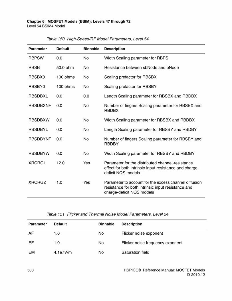
500 HSPICE® Reference Manual: MOSFET ModelsD-2010.12
Chapter 6: MOSFET Models (BSIM): Levels 47 through 72Level 54 BSIM4 Model
RBPSW 0.0 No Width Scaling parameter for RBPS
RBSB 50.0 ohm No Resistance between sbNode and bNode
RBSBX0 100 ohms No Scaling prefactor for RBSBX
RBSBY0 100 ohms No Scaling prefactor for RBSBY
RBSDBXL 0.0 0.0 Length Scaling parameter for RBSBX and RBDBX
RBSDBXNF 0.0 No Number of fingers Scaling parameter for RBSBX and RBDBX
RBSDBXW 0.0 No Width Scaling parameter for RBSBX and RBDBX
RBSDBYL 0.0 No Length Scaling parameter for RBSBY and RBDBY
RBSDBYNF 0.0 No Number of fingers Scaling parameter for RBSBY and RBDBY
RBSDBYW 0.0 No Width Scaling parameter for RBSBY and RBDBY
XRCRG1 12.0 Yes Parameter for the distributed channel-resistance effect for both intrinsic-input resistance and charge-deficit NQS models
XRCRG2 1.0 Yes Parameter to account for the excess channel diffusion resistance for both intrinsic input resistance and charge-deficit NQS models
Table 151 Flicker and Thermal Noise Model Parameters, Level 54
Parameter Default Binnable Description
AF 1.0 No Flicker noise exponent
EF 1.0 No Flicker noise frequency exponent
EM 4.1e7V/m No Saturation field
Table 150 High-Speed/RF Model Parameters, Level 54
Parameter Default Binnable Description

HSPICE® Reference Manual: MOSFET Models 501D-2010.12
Chapter 6: MOSFET Models (BSIM): Levels 47 through 72Level 54 BSIM4 Model
KF 0.0 A2-EFs1-EFF No Flicker noise coefficient
NOIA 6.25e41
(eV)-1s1-EFm-3 for NMOS; 6.188e40
(eV)-1s1-EFm-3 for PMOS
No Flicker noise parameter A
NOIB 3.125e26
(eV)-1s1-EFm-1 for NMOS; 1.5e25
(eV)-1s1-EFm-1 for PMOS
No Flicker noise parameter B
NOIC 8.75 (eV)-1s1-EFm No Flicker noise parameter C
NTNOI 1.0 No Noise factor for short-channel devices for TNOIMOD=0 only
TNOIA 1.5 No Coefficient of the channel-length dependence of the total channel thermal noise
TNOIB 3.5 No Channel-length dependence parameter for partitioning the channel thermal noise
Table 152 Layout-Dependent Parasitics Model Parameters, Level 54
Parameter Default Binnable Description
DMCG 0.0m No Distance from the S/D contact center to the gate edge
DMCGT 0.0m No DMCG of the test structures
DMCI DMCG No Distance from the S/D contact center to the isolation edge in the channel-length direction
Table 151 Flicker and Thermal Noise Model Parameters, Level 54
Parameter Default Binnable Description

502 HSPICE® Reference Manual: MOSFET ModelsD-2010.12
Chapter 6: MOSFET Models (BSIM): Levels 47 through 72Level 54 BSIM4 Model
DMDG 0.0m No Same as DMCG, but for merged devices only
DWJ DWC (in CVmodel)
No Offset of the S/D junction width
MIN 0 No Minimize the number of drain or source diffusions for even-number fingered device
NF 1 No Number of device figures
NGCON 1 No Number of gate contacts
XGL 0.0m No Offset of the gate length due to variations in patterning
XGW 0.0m No Distance from the gate contact to the channel edge
Table 153 Asymmetric Source/Drain Junction Diode Model Parameters, Level 54
Parameter Default Binnable Description
BVD BVD=BVS No Breakdown voltage
BVS BVS=10.0V No Breakdown voltage
CJD CJD=CJS No Bottom junction capacitance per unit area at zero bias
CJS CJS=5.0e-4 F/m2 No Bottom junction capacitance per unit area at zero bias
CJSWD CJSWD=CJSWS No Isolation-edge sidewall junction capacitance per unit length
CJSWGD CJSWGD=CJSWS No Gate-edge sidewall junction capacitance per unit length
Table 152 Layout-Dependent Parasitics Model Parameters, Level 54
Parameter Default Binnable Description

HSPICE® Reference Manual: MOSFET Models 503D-2010.12
Chapter 6: MOSFET Models (BSIM): Levels 47 through 72Level 54 BSIM4 Model
CJSWGS CJSWGS=CJSWS No Gate-edge sidewall junction capacitance per unit length
CJSWS CJSWS=5.0e-10 F/m
No Isolation-edge sidewall junction capacitance per unit length
IJTHDFWD IJTHDFWD=IJTHSFWD
No Limiting current in the forward bias region
IJTHDREV IJTHDREV=IJTHSREV
No Limiting current in the reverse bias region
IJTHSFWD IJTHSFWD=0.1A No Limiting current in the forward bias region
IJTHSREV IJTHSREV=0.1A No Limiting current in the reverse bias region
JSD JSD=JSS No Bottom junction reverse saturation current density
JSS JSS=1.0e-4A/m2 No Bottom junction reverse saturation current density
JSWD JSWD=JSWS No Isolation-edge sidewall reverse saturation current density
JSWGD JSWGD=JSWGS No Gate-edge sidewall reverse saturation current density
JSWGS JSWGS=0.0A/m No Gate-edge sidewall reverse saturation current density
JSWS JSWS=0.0A/m No Isolation-edge sidewall reverse saturation current density
MJD MJD=MJS No Bottom junction capacitance grading coefficient
MJS MJS=0.5 No Bottom junction capacitance grading coefficient
Table 153 Asymmetric Source/Drain Junction Diode Model Parameters, Level 54
Parameter Default Binnable Description

504 HSPICE® Reference Manual: MOSFET ModelsD-2010.12
Chapter 6: MOSFET Models (BSIM): Levels 47 through 72Level 54 BSIM4 Model
MJSWD MJSWD=MJSWS No Isolation-edge sidewall junction capacitance grading coefficient
MJSWGD MJSWGD=MJSWS No Gate-edge sidewall junction capacitance grading coefficient
MJSWGS MJSWGS=MJSWS No Gate-edge sidewall junction capacitance grading coefficient
MJSWS MJSWS=0.33 No Isolation-edge sidewall junction capacitance grading coefficient
PBD PBD=PBS No Bottom junction built-in potential
PBS PBS=1.0V No Bottom junction built-in potential
PBSWD PBSWD=PBSWS No Isolation-edge sidewall junction built-in potential
PBSWGD PBSWGD=PBSWS No Gate-edge sidewall junction built-in potential
PBSWGS PBSWGS=PBSWS No Gate-edge sidewall junction built-in potential
PBSWS PBSWS=1.0V No Isolation-edge sidewall junction built-in potential
XJBVD XJBVD=XJBVS No Fitting parameter for the diode breakdown
XJBVS XJBVS=1.0 No Fitting parameter for the diode breakdown
Table 154 Temperature Dependence Parameters, Level 54
Parameter Default Binnable Description
AT 3.3e4m/s Yes Temperature coefficient for the saturation velocity
Table 153 Asymmetric Source/Drain Junction Diode Model Parameters, Level 54
Parameter Default Binnable Description

HSPICE® Reference Manual: MOSFET Models 505D-2010.12
Chapter 6: MOSFET Models (BSIM): Levels 47 through 72Level 54 BSIM4 Model
KT1 -0.11V Yes Temperature coefficient for the threshold voltage
KT1L 0.0Vm Yes Channel length dependence of the temperature coefficient for the threshold voltage
KT2 0.022 Yes Body-bias coefficient of the Vth temperature effect
NJS, NJD NJS=1.0; NJD=NJS
No Emission coefficients of junction for the source and drain junctions
PRT 0.0ohm-m Yes Temperature coefficient for Rdsw
TCJ 0.0K-1 No Temperature coefficient of CJ
TCJSW 0.0K-1 No Temperature coefficient of CJSW
TCJSWG 0.0K-1 No Temperature coefficient of CJSWG
TNOM 27° Χ No Temperature at which simulation extracts parameters
TPB 0.0V/K No Temperature coefficient of PB
TPBSW 0.0V/K No Temperature coefficient of PBSW
TPBSWG 0.0V/K No Temperature coefficient of PBSWG
TRD 0.0 1K-1 No Temperature coefficient for the drain diffusion and the Rd contact resistances.
TRS 0.0 1/K No Temperature coefficient for the source diffusion and the Rs contact resistances.
TVFBSDOFF 0.0K-1 Yes Temperature coefficient of VFBSDOFF
TVOFF 0.0K-1 Yes Temperature coefficient of VOFF
Table 154 Temperature Dependence Parameters, Level 54
Parameter Default Binnable Description

506 HSPICE® Reference Manual: MOSFET ModelsD-2010.12
Chapter 6: MOSFET Models (BSIM): Levels 47 through 72Level 54 BSIM4 Model
UA1 1.0e-9m/V Yes Temperature coefficient for UA
UB1 -1.0e-18 (m/V2) Yes Temperature coefficient for UB
UC1 0.056/V-1 for MOBMOD=1;
0.056e-9m/V2 for MOBMOD=0 and 2
Yes Temperature coefficient for UC
UD1 0.0(1/m)2 Yes Temperature coefficient for UD
UTE -1.5 Yes Mobility temperature exponent
XTIS, XTID XTIS=3.0; XTID=XTIS
No Junction current temperature exponents for the source and drain junctions
Table 155 Well Proximity Effect Parameters, Level 54
Parameter Default Binnable Description
K2WE 0.0 Yes K2 shift factor for well proximity effect
KU0WE 0.0 Yes Mobility degradation factor for well proximity effect
KVTH0WE 0.0 Yes Threshold shift factor for well proximity effect
SC 0.0[m] No Distance to a single well edge
SCA 0.0 No Integral of the first distribution function for scattered well dopant
SCB 0.0 No Integral of the second distribution function for scattered well dopant
SCC 0.0 No Integral of the third distribution function for scattered well dopant
SCREF 1e-6[m] No Reference distance to calculate SCA, SCB, and SCC
Table 154 Temperature Dependence Parameters, Level 54
Parameter Default Binnable Description

HSPICE® Reference Manual: MOSFET Models 507D-2010.12
Chapter 6: MOSFET Models (BSIM): Levels 47 through 72Level 54 BSIM4 Model
WEB 0.0 No Coefficient for SCB
WEC 0.0 No Coefficient for SCC
Table 156 dW and dL Parameters, Level 54
Parameter Default Binnable Description
LL 0.0mLLN No Coefficient of the length dependence for the length offset
LLC LL No Coefficient of the length dependence for the CV channel length offset
LLN 1.0 No Power of the length dependence for the length offset
LW 0.0mLWN No Coefficient of the width dependence for the length offset
LWC LW No Coefficient of the width dependence for the CV channel length offset
LWL 0.0 mLWN+LLN No Coefficient of the length and width cross term dependence for the length offset
LWLC LWL No Coefficient of the length and width cross-term dependence for the CV channel length offset
LWN 1.0 No Power of the width dependence, length offset
WL 0.0μΩΛ Ν No Coefficient of the length dependence of the width offset
WLC WL No Coefficient of the length dependence for the CV channel width offset
WLN 1.0 No Power of the length dependence of the width offset
Table 155 Well Proximity Effect Parameters, Level 54
Parameter Default Binnable Description

508 HSPICE® Reference Manual: MOSFET ModelsD-2010.12
Chapter 6: MOSFET Models (BSIM): Levels 47 through 72Level 54 BSIM4 Model
WW 0.0mWWN No Coefficient of the width dependence of the width offset
WWC WW No Coefficient of the width dependence for the CV channel width offset
WWL 0.0 mWWN+WLN No Coefficient of the length and width cross term dependence for the width offset
WWLC WWL No Coefficient of the length and width cross-term dependence for the CV channel width offset
WWN 1.0 No Power of the width dependence of the width offset
Table 157 Range Parameters for Model Application, Level 54
Parameter Default Binnable Description
LMIN 0.0μ No Minimum channel length
LMAX 1.0m No Maximum channel length
WMIN 0.0m No Minimum channel width
WMAX 1.0m No Maximum channel width
Table 156 dW and dL Parameters, Level 54
Parameter Default Binnable Description

HSPICE® Reference Manual: MOSFET Models 509D-2010.12
Chapter 6: MOSFET Models (BSIM): Levels 47 through 72Level 54 BSIM4 Model
Version 4.6 FeaturesThe current HSPICE release supports BSIM version 4.6.0, including the following features:■ The IGISL and IGIDL modules have independent model parameters (as
opposed to v. 4.5, in which the GIDL and GISL leakage current modules shared the parameter set).
■ The parameters for the source and drain side junction diode current due to the trap-assisted tunneling current in space-change region are fully separated.
■ The parameters for the gate tunneling current in the S/D overlap diffusion regions (Igs/Igd) are separated.
In addition three bug fixes are implemented in this version. ■ The implementation of coulomb scattering in mobility model has been
changed to avoid the non-monoticity in drain current as a function of gate voltage. Also the default value of parameter has been changed to 0.
■ The accuracy of RgateMod = 2 has been improved by accounting correctly the contribution from Rgate to overall noise. The change has been made in b4noi.c
■ The default value for the model parameter VFB was missing. The default value of the parameter VFB has ben now set to -1.0V in b4set.c
Version 4.6.1 FeaturesCompared with BSIM4.6.0, several new features are added in this version.■ New material model is introduced for the predictive modeling of Non-SiO2
insulator, Non-Poly Silicon gate and Non-silicon channel. The following new parameters are added:
• MTRLMOD: New material model selector
• PHIG, EPSRGATE: non-poly silicon gate parameters
• EOT, VDDEOT: non-SiO2 gate dielectric
• EASUB, EPSRSUB, NI0SUB, BG0SUB, TBGASUB, TBGBSUB, ADOS, BDOS: Non-silicon channel parameters

510 HSPICE® Reference Manual: MOSFET ModelsD-2010.12
Chapter 6: MOSFET Models (BSIM): Levels 47 through 72Level 54 BSIM4 Model
■ Mobility model (MOBMOD = 0 and MOBMOD = 1) has been improved through predictive modeling of vertical electric field. The improved mobility model is selected through MTRLMOD = 1 for backward compatibility.
■ GIDL/GISL models are improved through an improved definition of flatband voltages at S/D ends. The improved GISL/GIDL model is selected through MTRLMOD = 1 for backward compatibility.
■ The Poly-depletion model is modified to account for new gate and gate-insulator materials.
■ C-V model has been improved by adding a new VgsteffCV definition through CVCHARGEMOD = 1. Six new parameters have been added: CVCHARGEMOD, MINVCV, LMINVCV, WMINCV, PMINVCV and VOFFCVL
■ The following bugs have been fixed:
• An error in the derivative calculation of dVdseffCV_dVb has been fixed for CAPMOD = 1 and CAPMOD = 2 in b4ld.c
• The warning limits for NOFF and VOFFCV have been removed from b4check.c.
Version 4.6.2 Features and UpdatesThe v. 4.6.2 release added the following features and bug fixes:■ Mobility model (mobMod=3) added to enhance the modeling of Coulombic
scattering in the high-k/metal gate transistors.■ Trap assisted tunneling (TAT) has been improved to include the width
dependence. A new model parameter JTWEFF is introduced and set to zero to maintain the backward compatibility.
■ Bug fixes include:
• Output Conductance Model: VASCBE:A division by zero bug in the output conductance calculation is fixed.
• Thermal Noise Model (tnoiMod=0): The scaling factor NF is added to the equivalent resistance Rds/NF.
• Negative Thermal Noise (tnoiMod=1) The noise spectral density will not be negative now.

HSPICE® Reference Manual: MOSFET Models 511D-2010.12
Chapter 6: MOSFET Models (BSIM): Levels 47 through 72Level 57 UC Berkeley BSIM3-SOI Model
• Source/Drain Bulk Junction Capacitance: The source/drain bulk junction capacitance will not be discontinuous when Vbs/Vbd is zero. The S/D junction sidewall capacitance along the isolation edge is set to zero if they are negative.
• Derivative Issue in Capacitance Model (capMod=0): An error in the derivative calculation of dVgs_eff_dVg has been fixed.
• Toxp Calculation (mtrlMod=1): The physical oxide thickness should be lay-out independent.
• Source/Drain Resistance: A division by zero bug in the Rend calculation is fixed.
• Typo of SC: SCA is a typo of SC in b4.c
• Drain/Body Breakdown Voltage: The reset value of drain/body breakdown voltage will not cause non-convergence now. Some other similar bugs have also been fixed.
Version 4.6.3 UpdateThe only change in BSIM4.6.3 compared with BSIM4.6.2 was the refinement of the calculation below.
pParam->BSIM4litl = sqrt(3.0 * 3.9 / epsrox * pParam->BSIM4xj * toxe)
Level 54 BSIM4 Template Output ListFor a list of output template parameters in the MOSFET models, and which parameters this model supports, see Table 4 on page 22.
Level 57 UC Berkeley BSIM3-SOI Model
The UC Berkeley SOI model (BSIM3SOI) supports Fully Depleted (FD), Partially Depleted (PD), and Dynamically Depleted (DD) SOI devices of which BSIM3PD2.0.1 for PD SOI devices is Synopsys MOSFET Level 57. For a description of this model, see the BSIM3PD2.0 MOSFET MODEL User’s Manual.

512 HSPICE® Reference Manual: MOSFET ModelsD-2010.12
Chapter 6: MOSFET Models (BSIM): Levels 47 through 72Level 57 UC Berkeley BSIM3-SOI Model
Level 57 uses the UCB Version 2.2.3 model, which includes a separate set of the geometry-dependence parameters (LLC, LWC, LWLC, WLC, WWC, and WWLC) to calculate LeffCV and WeffCV.
Level 57 also includes a new Full-Depletion (FD) module (soiMod=1). This module provides a better fit to FD SOI devices. As soiMod=0 (default), the model is identical to previous BSIMSOI PD models. This module also includes gate to channel/drain/source tunneling currents and overlap components.
The following enhancements to the BSIMSOI PD version were made starting in the BSIMSOI 3.0 version: ■ If the self-heating model is on, simulation calculates the channel surface
potential.■ NDIF includes parameter Compared with BSIM4.6.1, several new features
are added in this version.■ An error in the derivative calculation of dVgs_eff_dVg has been fixed.■ The reset value of drain/body breakdown voltage will not cause non-
convergence now. Some other similar bugs have also been fixed.■ The DELTOX parameter in the MOS active element (M) models the relative
variation on the trans conductance (oxide thickness) of the MOS in Monte Carlo analysis.
The following sections discuss these topics:■ General Syntax for BSIM3-SOI Model■ Level 57 Model Parameters■ Parameter Range Limit for BSIM4SOI Level 57■ Level 57 Template Output■ Level 57 Updates to BSIM3-SOI PD versions 2.2, 2.21, and 2.22■ UCB BSIMSOI3.1■ New Features in BSIMSOIv3.2
General Syntax for BSIM3-SOI Model The general syntax for including a BSIM3-SOI model element in a netlist is:
Mxxx nd ng ns ne [np] [nb] [nT] mname [L=val] [W=val]+ [M=val] [NRD=val] [AD=val] [AS=val] [PD=val] [PS=val]+ [VER_CONTROL=0|1][NRS=val] [NRB=val] [RTH0=val] [NBC=val]
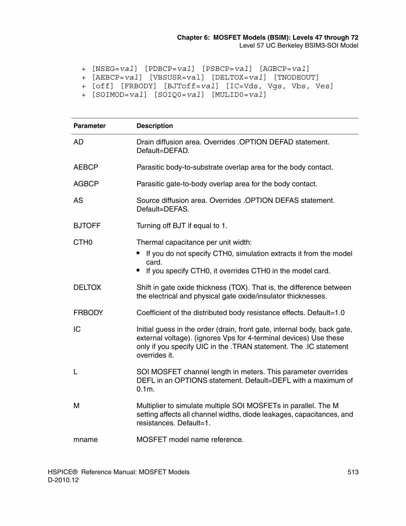
HSPICE® Reference Manual: MOSFET Models 513D-2010.12
Chapter 6: MOSFET Models (BSIM): Levels 47 through 72Level 57 UC Berkeley BSIM3-SOI Model
+ [NSEG=val] [PDBCP=val] [PSBCP=val] [AGBCP=val]+ [AEBCP=val] [VBSUSR=val] [DELTOX=val] [TNODEOUT]+ [off] [FRBODY] [BJToff=val] [IC=Vds, Vgs, Vbs, Ves]+ [SOIMOD=val] [SOIQ0=val] [MULID0=val]
Parameter Description
AD Drain diffusion area. Overrides .OPTION DEFAD statement. Default=DEFAD.
AEBCP Parasitic body-to-substrate overlap area for the body contact.
AGBCP Parasitic gate-to-body overlap area for the body contact.
AS Source diffusion area. Overrides .OPTION DEFAS statement. Default=DEFAS.
BJTOFF Turning off BJT if equal to 1.
CTH0 Thermal capacitance per unit width:■ If you do not specify CTH0, simulation extracts it from the model
card.■ If you specify CTH0, it overrides CTH0 in the model card.
DELTOX Shift in gate oxide thickness (TOX). That is, the difference between the electrical and physical gate oxide/insulator thicknesses.
FRBODY Coefficient of the distributed body resistance effects. Default=1.0
IC Initial guess in the order (drain, front gate, internal body, back gate, external voltage). (ignores Vps for 4-terminal devices) Use these only if you specify UIC in the .TRAN statement. The .IC statement overrides it.
L SOI MOSFET channel length in meters. This parameter overrides DEFL in an OPTIONS statement. Default=DEFL with a maximum of 0.1m.
M Multiplier to simulate multiple SOI MOSFETs in parallel. The M setting affects all channel widths, diode leakages, capacitances, and resistances. Default=1.
mname MOSFET model name reference.

514 HSPICE® Reference Manual: MOSFET ModelsD-2010.12
Chapter 6: MOSFET Models (BSIM): Levels 47 through 72Level 57 UC Berkeley BSIM3-SOI Model
Mxxx SOI MOSFET element name. Must begin with M, followed by up to 1023 alphanumeric characters.
nb Internal body node name or number.
NBC Number of body contact isolation edge.
nd Drain terminal node name or number.
ne Back gate (or substrate) node name or number.
ng Front gate node name or number.
np External body contact node name or number.
NRB Number of squares for the body series resistance.
NRD NRD (Number of squares of drain diffusion for resistance calculations) overrides .OPTION DEFNRD.
For nonCMI models such as BSIM3 etc… Default=DEFNRD, if you set ACM=0 or 1 model parameter. Default=0.0, if you set ACM=2 or 3
For CMI models such as BSIM4 etc… Default=1.0
NRS NRS (Number of squares of source diffusion for resistance calculations) overrides .OPTION DEFNRS.
For nonCMI models such as BSIM3 etc… Default=DEFNRS, if you set ACM=0 or 1 model parameter. Default=0.0, if you set ACM=2 or 3
For CMI models such as BSIM4 etc… Default=1.0
ns Source terminal node name or number.
NSEG Number of segments for partitioning the channel width.
nT Temperature node name or number.
OFF Sets the initial condition of the element to OFF in DC analysis.
PD Drain junction perimeter, including channel edge. Overrides .OPTION DEFPD.
PDBCP Parasitic perimeter length for the body contact a the drain side.
Parameter Description

HSPICE® Reference Manual: MOSFET Models 515D-2010.12
Chapter 6: MOSFET Models (BSIM): Levels 47 through 72Level 57 UC Berkeley BSIM3-SOI Model
PS Source junction perimeter including channel edge. Overrides .OPTION DEFPS.
PSBCP Parasitic perimeter length for the body contact at the source side.
RTH0 Thermal resistance per unit width:■ If you do not specify RTH0, simulation extracts it from the model
card.■ If you specify RTH0, it overrides RTH0 in the model card.
SOIMOD SOI model selector
If SOIMOD is not specified, it's extracted from the model card
If SOIMOD is specified, it overrides SOIMOD in the model card
SOIQ0 Floating body charge initialization. This parameter is set for the BQI algorithm of a floating body node.
TNODEOUT Temperature node flag indicating the use of the T node.
VBSUSR Optional initial Drain/Body Breakdown Voltage of Vbs that you specify for transient analysis.
W MOSFET channel width in meters. This parameter overrides DEFW in an OPTIONS statement. Default=DEFW.
MULID0 Scaling factor of drain current, the default is 1.0.
VER_CONTROL ■ VER_CONTROL=0: (Default) Version control is off■ VER_CONTROL=1: Version control is on; the simulation will abort
for non-supported version
Parameter Description

516 HSPICE® Reference Manual: MOSFET ModelsD-2010.12
Chapter 6: MOSFET Models (BSIM): Levels 47 through 72Level 57 UC Berkeley BSIM3-SOI Model
■ If you do not set TNODEOUT, you can specify four nodes for a device to float the body. Specifying five nodes implies that the fifth node is the external body contact node with a body resistance between the internal and external terminals. This configuration applies to a distributed body resistance simulation.
■ If you set TNODEOUT, simulation interprets the last node as the temperature node. You can specify five nodes to float the device. Specifying six nodes implies body contact. Seven nodes is a body-contacted case with an accessible internal body node. You can use the temperature node to simulate thermal coupling.
Level 57 Model Parameters
Table 158 Model Control Parameters, Level 57
Parameter Unit Default Description
capmod - 2 Flag for the short channel capacitance model
MOBMOD - 1 Mobility model selector
noimod - 1 Flag for the noise model
SHMOD - 0 Flag for self-heating:
0 - no self-heating1 - self-heating
Table 159 Process Parameters, Level 57
Parameter Unit Default Description
DTOXCV(capmod=3 only)
Difference between the electrical and physical gate oxide thicknesses, due to the effects of the gate poly-depletion and the finite channel charge layer thickness.
Nch 1/cm3 1.7e17 Channel doping concentration
Ngate 1/cm3 0 Poly gate doping concentration

HSPICE® Reference Manual: MOSFET Models 517D-2010.12
Chapter 6: MOSFET Models (BSIM): Levels 47 through 72Level 57 UC Berkeley BSIM3-SOI Model
Nsub 1/cm3 6.0e16 Substrate doping concentration
Tbox m 3.0e-7 Buried oxide thickness
Tox m 1.0e-8 Gate oxide thickness
Tsi m 1.0e-7 Silicon film thickness
Xj m - S/D junction depth
Table 160 DC Parameters, Level 57
Parameter Unit Default Description
a0 - 1.0 Bulk charge effect coefficient for the channel length
A1 1/V 0.0 First non-saturation effect parameter
A2 - 1.0 Second non-saturation effect parameter
Aely V/m 0 Channel length dependency of the early voltage for the bipolar current
Agidl 1/W 0.0 GIDL constant
ags 1/V 0.0 Gate bias coefficient of Abulk
Ahli - 0 High-level injection parameter for the bipolar current
alpha0 m/V 0.0 First parameter of the impact ionization current
b0 m 0.0 Bulk charge effect coefficient for the channel width
b1 m 0.0 Bulk charge effect width offset
Table 159 Process Parameters, Level 57
Parameter Unit Default Description

518 HSPICE® Reference Manual: MOSFET ModelsD-2010.12
Chapter 6: MOSFET Models (BSIM): Levels 47 through 72Level 57 UC Berkeley BSIM3-SOI Model
beta0 1/V 0.0 First Vds dependence parameter of the impact ionization current
beta1 - 0.0 Second Vds dependence parameter of the impact ionization current
beta2 V 0.1 Third Vds dependence parameter of the impact ionization current
Bgidl V/m 0.0 GIDL exponential coefficient
cdsc F/m2 2.4e-4 Drain/source to the channel coupling capacitance
cdscb F/m2 0 Body-bias sensitivity of cdsc
cdscd F/m2 0 Drain-bias sensitivity of cdsc
cit F/m2 0.0 Interface trap capacitance
delta - 0.01 Effective Vds parameter
drout - 0.56 L dependence coefficient of the DIBL correction parameter in Rout
dsub - 0.56 DIBL coefficient exponent
Dvt0 - 2.2 First coefficient of the short-channel effect on Vth
dvt0w - 0 First coefficient of the narrow width effect on Vth for a small channel length
dvt1 - 0.53 Second coefficient of the short-channel effect on Vth
dvt1w - 5.3e6 Second coefficient of the narrow width effect on Vth for a small channel length
dvt2 1/V -0.032 Body-bias coefficient of the short-channel effect on Vth
Table 160 DC Parameters, Level 57
Parameter Unit Default Description

HSPICE® Reference Manual: MOSFET Models 519D-2010.12
Chapter 6: MOSFET Models (BSIM): Levels 47 through 72Level 57 UC Berkeley BSIM3-SOI Model
dvt2w 1/V -0.032 Body-bias coefficient of the narrow width effect on Vth for a small channel length
dwb m/V1/2 0.0 Coefficient of the substrate body bias dependence of Weff
dwbc m 0.0 Width offset for the body contact isolation edge
dwg m/V 0.0 Coefficient of the gate dependence of Weff
esati V/m 1.e7 Saturation channel electric field for the impact ionization current
eta0 - 0.08 DIBL coefficient in the subthreshold region
etab 1/V -0.07 Body-bias coefficient for the DIBL effect in the subthreshold region
fbjtii - 0.0 Fraction of the bipolar current affecting the impact ionization
Isbjt A/m2 1.0e-6 BJT injection saturation current
Isdif A/m2 0 Body to source/drain injection saturation current
Isrec A/m2 1.0e-5 Recombination in the depletion saturation current
Istun A/m2 0.0 Reverse tunneling saturation current
k1 V1/2 0.6 First-order body effect coefficient
k1w1 m 0 First-order effect width dependent parameter
k1w2 m 0 Second-order effect width dependent parameter
k2 - 0 Second-order body effect coefficient
k3 - 0 Narrow coefficient
Table 160 DC Parameters, Level 57
Parameter Unit Default Description

520 HSPICE® Reference Manual: MOSFET ModelsD-2010.12
Chapter 6: MOSFET Models (BSIM): Levels 47 through 72Level 57 UC Berkeley BSIM3-SOI Model
k3b 1/V 0 Body effect coefficient of k3
kb1 - 1 Backgate body charge coefficient
keta 1/V -0.6 Body-bias coefficient of the bulk charge effect
Ketas V 0.0 Surface potential adjustment for the bulk charge effect
Lbjt0 m 0.2e-6 Reference channel length for the bipolar current
lii - 0 Channel length dependence parameter for the impact ionization current
lint m 0.0 Length offset fitting parameter from I-V without bias
Ln m 2.0e-6 Electron/hole diffusion length
Nbjt - 1 Power coefficient of the channel length dependency for the bipolar current
NdioDE - 1.0 Diode non-ideality factor
nfactor - 1 Subthreshold swing factor
Ngidl V 1.2 GIDL Vds enhancement coefficient
nlx m 1.74e-7 Lateral non-uniform doping parameter
Nrecf0 - 2.0 Recombination non-ideality factor at the forward bias
Nrecr0 - 10 Recombination non-ideality factor at the reversed bias
Ntun - 10.0 Reverse tunneling non-ideality factor
pclm - 1.3 Channel length modulation parameter
Table 160 DC Parameters, Level 57
Parameter Unit Default Description

HSPICE® Reference Manual: MOSFET Models 521D-2010.12
Chapter 6: MOSFET Models (BSIM): Levels 47 through 72Level 57 UC Berkeley BSIM3-SOI Model
PDIBLC1 - 0.39 Correction parameter for the DIBL effect of the first output resistance
pdiblc2 - 0.0086 Correction parameter for the DIBL effect of the second output resistance
prwb 1/V1 0 Body effect coefficient of Rdsw
prwg 1/V1/2 0 Gate-bias effect coefficient of Rdsw
pvag - 0.0 Gate dependence of the Early voltage
Rbody ohm/m2 0.0 Intrinsic body contact sheet resistance
Rbsh ohm/m2 0.0 Extrinsic body contact sheet resistance
rdsw 100 Parasitic resistance per unit width
rsh ohm/square
0.0 Source/drain sheet resistance in ohm per square
sii0 1/V 0.5 First Vgs dependence parameter for the impact ionization current
sii1 1/V 0.1 Second Vgs dependence parameter for the impact ionization current
sii2 1/V 0 Third Vgs dependence parameter for the impact ionization current
siid 1/V 0 Vds dependence parameter of the drain saturation voltage for the impact ionization current
tii - 0 Temperature dependence parameter for the impact ionization current
u0 cm2/(V-sec)
NMOS-670 PMOS-250
Mobility at Temp=Tnom
Table 160 DC Parameters, Level 57
Parameter Unit Default Description
Ω*μmwr

522 HSPICE® Reference Manual: MOSFET ModelsD-2010.12
Chapter 6: MOSFET Models (BSIM): Levels 47 through 72Level 57 UC Berkeley BSIM3-SOI Model
ua m/V 2.25e-9 First-order mobility degradation coefficient
ub (m/V)2 5.87e-19 Second-order mobility degradation coefficient
uc 1/V -0.0465 Body-effect of the mobility degradation coefficient
Vabjt V 10 Early voltage for the bipolar current
vdsatii0 V 0.9 Nominal drain saturation voltage at threshold for the impact ionization current
VECB v 0.026v Electron tunneling from the conduction band
VEVB v 0.075v Electron tunneling from the valence band
voff v -0.08 Offset voltage in the subthreshold region for large W and L
Vrec0 V 0.0 Voltage dependent parameter for the recombination current
vsat m/sec 8e4 Saturation velocity at Temp=Tnom
vth0 v NMOS 0.7PMOS -0.7
Threshold voltage @ Vbs=0 for a long, wide device
Vtun0 V 0.0 Voltage dependent parameter for the tunneling current
w0 m 0 Narrow width parameter
wint m 0.0 Width offset fitting parameter from I-V without bias
wr - 1 Width offset from Weff for the Rds calculation
Table 160 DC Parameters, Level 57
Parameter Unit Default Description

HSPICE® Reference Manual: MOSFET Models 523D-2010.12
Chapter 6: MOSFET Models (BSIM): Levels 47 through 72Level 57 UC Berkeley BSIM3-SOI Model
Table 161 AC and Capacitance Parameters, Level 57
Parameter Unit Default Description
acde m/V 1.0 Exponential coefficient for the charge thickness in the CapMod=3 for the accumulation and depletion regions
asd V 0.3 Smoothing parameter for the source/drain bottom diffusion
cf F/m cal. Fringing field capacitance of the gate-to-source/drain
cgdl F/m 0.0 Overlap capacitance for the lightly-doped drain-gate region
cgdo F/m 0 Non LDD region drain-gate overlap capacitance per channel length
CGEO F/m 0 Gate substrate overlap capacitance per unit channel length
cgsl F/m 0.0 Overlap capacitance for the lightly-doped source-gate region
cgso F/m calculated
Non LDD region source-gate overlap capacitance per channel length
cjswg F/m2 1.e-10 Source/drain (gate side) sidewall junction capacitance per unit width (normalized to 100nm Tsi)
ckappa F/m 0.6 Coefficient for the fringing field capacitance for the overlap capacitance in the lightly-doped region
clc m 0.1e-7 Constant term for the short-channel model
cle - 0.0 Exponential term for the short-channel model
csdesw F/m 0.0 Fringing capacitance per unit length for the source/drain sidewall
csdmin V cal. Minimum capacitance for the source/drain bottom diffusion
delvt V 0.0 Threshold voltage adjustment for C-V

524 HSPICE® Reference Manual: MOSFET ModelsD-2010.12
Chapter 6: MOSFET Models (BSIM): Levels 47 through 72Level 57 UC Berkeley BSIM3-SOI Model
dlbg m 0 Length offset fitting parameter for the backgate charge
dlc m lint Length offset fitting parameter for the gate charge
dlcb m lint Length offset fitting parameter for the body charge
dwc m wint Width offset fitting parameter from C-V
fbody - 1.0 Scaling factor for the body charge
Ldif0 - 1 Channel length dependency coefficient of the diffusion cap.
mjswg V 0.5 Grading coefficient of the source/drain (gate side) sidewall junction capacitance
moin V1/2 15.0 Coefficient for the gate-bias dependent surface potential
Ndif - -1 Power coefficient of the channel length dependency for the diffusion capacitance
pbswg V 0.7 Built-in potential of the source/drain (gate side) sidewall junction capacitance
tt second 1ps Diffusion capacitance transit time coefficient
vsdfb V cal. Flatband voltage for the source/drain bottom diffusion capacitance
vsdth V cal. Threshold voltage for the source/drain bottom diffusion capacitance
xpart - 0 Charge partitioning rate flag
Table 161 AC and Capacitance Parameters, Level 57
Parameter Unit Default Description

HSPICE® Reference Manual: MOSFET Models 525D-2010.12
Chapter 6: MOSFET Models (BSIM): Levels 47 through 72Level 57 UC Berkeley BSIM3-SOI Model
Table 162 Temperature Parameters, Level 57
Parameter Unit Default Description
at m/sec 3.3e4 Temperature coefficient for Ua
cth0 moC/(W*s) 0 Normalized thermal capacity
kt1 V -0.11 Temperature coefficient for the threshold voltage
kt2 - 0.022 Body-bias coefficient of the threshold voltage temperature effect
ktil V*m 0 Channel length dependence of the temperature coefficient for the threshold voltage
Ntrecf - 0 Temperature coefficient for Nrecf
Ntrecr - 0 Temperature coefficient for Nrecr
prt-um
0 Temperature coefficient for Rdsw
rth0 moC/W 0 Normalized thermal resistance
tcjswg 1/K 0 Temperature coefficient of Cjswg
tnom oC 25 Temperature at which simulation expects parameters
tpbswg V/K 0 Temperature coefficient of Pbswg
ua1 m/V 4.31e-9 Temperature coefficient for Ua
ub1 (m/V)2 -7.61e-18 Temperature coefficient for Ub
uc1 1/V -0.056 Temperature coefficient for Uc
ute - -1.5 Mobility temperature exponent
xbjt - 1 Power dependence of jbjt on the temperature
xdif - XBJT Power dependence of jdif on the temperature
xrec - 1 Power dependence of jrec on the temperature
Ω

526 HSPICE® Reference Manual: MOSFET ModelsD-2010.12
Chapter 6: MOSFET Models (BSIM): Levels 47 through 72Level 57 UC Berkeley BSIM3-SOI Model
The parameters in Table 163 improve the BSIM3SOI model to address parasitic BJT-induced avalanche impact ionization current. Contact Synopsys for details.
Level 57 Notes:■ BSIMPD2.01 supports capmod=2 and 3 only. It does not support capmod=0
and 1.■ Modern SOI technology commonly uses source/drain extension or LDD. The
source/drain junction depth (Xj) can be different from the silicon film thickness (Tsi). By default, if you do not specify Xj, simulation sets it to Tsi. Xj cannot be greater than Tsi.
■ BSIMPD refers the substrate to the silicon below the buried oxide (not to the well region in BSIM3) to calculate the backgate flatband voltage (Vfbb) and the parameters related to the source/drain diffusion bottom capacitance (Vsdth, Vsdfb, Csdmin).
• Positive nsub means the same type of doping as the body.
xtun - 0 Power dependence of jtun on the temperature
Table 163 Avalanche Impact Ionization Parameters, Level 57
Parameter Unit Default Description Notes
IIMOD - 0 (original II model)
Impact ionization model selector =1 selects the new II model
EBJTII 1/V 0.0 Impact ionization parameter for BJT part -
CBJTII m/V 0.0 Length scaling parameter for II BJT part -
VBCI V 0.7 Internal B-C built-in potential -
ABJTII - 0.0 Exponent factor for avalanche current -
MBJTII - 0.4 Internal B-C grading coefficient
TVBCI - 0.0 Temperature coefficient for VBCI
Table 162 Temperature Parameters, Level 57
Parameter Unit Default Description

HSPICE® Reference Manual: MOSFET Models 527D-2010.12
Chapter 6: MOSFET Models (BSIM): Levels 47 through 72Level 57 UC Berkeley BSIM3-SOI Model
• Negative nsub means the opposite type of doping. ■ New W0FLK Parameter:
The following equation models the SPICE2 flicker noise current density, used in both UCB SOI code and the Synopsys Level=57 MOSFET model for noiMod=1 and 4:
Sid,f[I2/Hz]=KF*Ids^AF/(Cox*Leff^2*f^EF) -- (1)
However, if AF is not equal to unity, it does not scale properly with Weff, because Ids is approximately proportional to Weff. Also, without the HSPICE multiplicity factor (M factor) in equation (1), this model cannot simulate multiple transistors in parallel.
To solve these problems, HSPICE 2002.2 added a W0FLK (width normalizing) parameter, and corrects equation (1) as:
M*KF*[(Weff/W0FLK)(1-AF)]*Ids^AF/(Cox*Leff^2*f^EF) -- (2)
The default value of W0FLK is -1.0 to switch off the new width-scaling model. The unit is in meters.
The next equation handles the flicker noise model (noimod=1 & 4), depending on whether you specify W0FLK.
If W0FLK <=0.0 (the default case), then the flicker noise model of noiMod=1 and 4 uses this equation for backward compatibility.
M*KF*Ids^AF/(Cox*LeffA2*f^EF) -- (3)ELSE
M*KF*[(Weff/W0FLK)^(1-AF)]*Ids^AF/(Cox*Leff^2*f^EF)
Parameter Range Limit for BSIM4SOI Level 57Simulation reports either a warning or a fatal error if BSIM3v3 parameters fall outside predefined ranges. These range limitations prevent (or at least warn of) potential numerical problems.
To control the maximum number of simulation warning messages printing to the output file, use:
.OPTION WARNLIMIT=#
In the preceding .OPTION statement, # is the maximum number of warning messages that simulation reports. The default WARNLIMIT

528 HSPICE® Reference Manual: MOSFET ModelsD-2010.12
Chapter 6: MOSFET Models (BSIM): Levels 47 through 72Level 57 UC Berkeley BSIM3-SOI Model
The source/drain bulk junction capacitance will not be discontinuous when Vbs/Vbd is zero. The S/D junction sidewall capacitance along the isolation edge is set to zero if they are negative.
value is 1. In some cases (as noted in Table 164 below), simulation checks parameters only if you set the PARMAMCHK=1 model parameter.
Table 164 Model Parameter Range Limit, Level 57
Parameter Limits Comment
nlx < -leff fatal
tox tox+deltox < 0 fatal
toxm toxm+deltox < 0 fatal
tbox <= 0 fatal
npeak <= 0 fatal
ngate < 0, > 1e25 fatal
dvt1 < 0 fatal
dvt1w < 0 fatal
w0 w0+weff =0 fatal
dsub < 0 fatal
b1 b1+weff =0 fatal
u0 <= 0 fatal
delta < 0 fatal
vsat <= 0 fatal
pclm <= 0 fatal
drout < 0 fatal
clc < 0 fatal
noff =0 warn, set 1.0 If (version>3.1999) < 0.1, > 4.0 warn

HSPICE® Reference Manual: MOSFET Models 529D-2010.12
Chapter 6: MOSFET Models (BSIM): Levels 47 through 72Level 57 UC Berkeley BSIM3-SOI Model
moin < 5, > 25 warn
acde < 0.1, > 1.6 warn if (2.2299 < version < 3.1099) acde < 0.4 warn
moinFD < 5.0 warn if (version > 2.9999)
if paramchk=1 following parameter limit range is added
leff <= 5e-8 warn
leffcv <= 5e-8 warn
weff <= 1e-7 warn
weffcv <= 1e-7 warn
nlx < 0 warn
tox tox+deltox < 0 warn
npeak <= 1e15, >= 1e21 warn
nsub >= 1e21 warn
ngate 0 < ngate <= 1e18 warn
dvt0 < 0 warn
w0 w0+weff < 1e-7 warn
cdsc < 0 warn
nfactor < 0 warn
cdscd < 0 warn
eta0 <0 warn
b1 b1+weff<1e-7 warn
a2 < 0.01, > 1 warn
Table 164 Model Parameter Range Limit, Level 57
Parameter Limits Comment
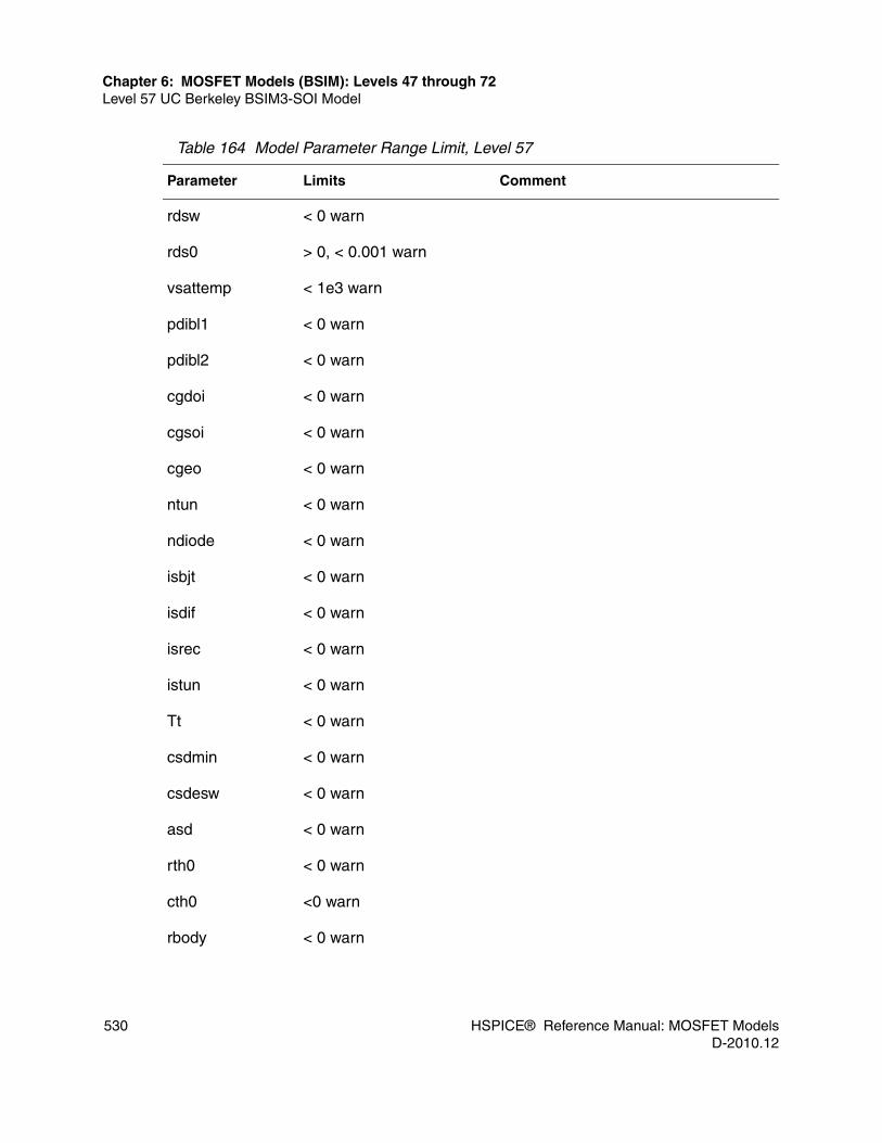
530 HSPICE® Reference Manual: MOSFET ModelsD-2010.12
Chapter 6: MOSFET Models (BSIM): Levels 47 through 72Level 57 UC Berkeley BSIM3-SOI Model
rdsw < 0 warn
rds0 > 0, < 0.001 warn
vsattemp < 1e3 warn
pdibl1 < 0 warn
pdibl2 < 0 warn
cgdoi < 0 warn
cgsoi < 0 warn
cgeo < 0 warn
ntun < 0 warn
ndiode < 0 warn
isbjt < 0 warn
isdif < 0 warn
isrec < 0 warn
istun < 0 warn
Tt < 0 warn
csdmin < 0 warn
csdesw < 0 warn
asd < 0 warn
rth0 < 0 warn
cth0 <0 warn
rbody < 0 warn
Table 164 Model Parameter Range Limit, Level 57
Parameter Limits Comment

HSPICE® Reference Manual: MOSFET Models 531D-2010.12
Chapter 6: MOSFET Models (BSIM): Levels 47 through 72Level 57 UC Berkeley BSIM3-SOI Model
rbsh < 0 warn
nigc <= 0 fatal if (version > 2.9999)
poxedge <= 0 fatal if (version > 2.9999)
pigcd <= 0 fatal if (version > 2.9999)
wth0 < 0 warn
rhalo < 0 warn
ntox < 0 warn
toxtref < 0 warn
ebg < 0 warn
nevb < 0 warn
vevb < 0 warn
alphaGB1 < 0 warn
BetaGB1 < 0 warn
vgb1 < 0 warn
necb < 0 warn
vecb < 0 warn
alphaGB2 < 0 warn
vgb2 < 0 warn
toxqm <= 0 warn
voxh < 0 warn
deltavox <= 0 warn
Table 164 Model Parameter Range Limit, Level 57
Parameter Limits Comment

532 HSPICE® Reference Manual: MOSFET ModelsD-2010.12
Chapter 6: MOSFET Models (BSIM): Levels 47 through 72Level 57 UC Berkeley BSIM3-SOI Model
k1w1 < 0 warn
k1w2 < 0 warn
ketas < 0 warn
dwbc < 0 warn
beta0 < 0 warn
beta1 < 0 warn
beta2 < warn
tii < 0 warn
lii < 0 warn
sii1 < 0 warn
sii2 < 0 warn
siid < 0 warn
fbjtii < 0 warn
vrec0 < 0 warn
vtun0 < 0 warn
nbjt < 0 warn
aely < 0 warn
ahli < 0 warn
rbody < 0 warn
rbsh < 0 warn
ntred < 0 warn
Table 164 Model Parameter Range Limit, Level 57
Parameter Limits Comment

HSPICE® Reference Manual: MOSFET Models 533D-2010.12
Chapter 6: MOSFET Models (BSIM): Levels 47 through 72Level 57 UC Berkeley BSIM3-SOI Model
Level 57 Template OutputFor a list of output template parameters in the MOSFET models, and which parameters this model supports, see Table 4 on page 22.
ntrecf < 0 warn
ndif < 0 warn if (version <= 2.9999)
tcjswg < 0 warn if (version <= 2.9999)
tpbswg < 0 warn if (version <= 2.9999)
acde < 0.4, > 1.6 warn if (version > 3.1099) acde < 0.1 warn
moin < 5, > 25 warn
dlbg < 0 warn
agidl < 0 warn
bgidl < 0 warn
ngidl < 0 warn
esatii < 0 warn Should be within (0,1)
xj > tsi warn
capmod < 2 warn
Table 164 Model Parameter Range Limit, Level 57
Parameter Limits Comment
534 HSPICE® Reference Manual: MOSFET ModelsD-2010.12
Chapter 6: MOSFET Models (BSIM): Levels 47 through 72Level 57 UC Berkeley BSIM3-SOI Model
Level 57 Updates to BSIM3-SOI PD versions 2.2, 2.21, and 2.22■ BSIM PD version 2.2 enhances the model flexibility and accuracy from PD
version 2.0, and the following are its major features.
• Gate-body tunneling (substrate current) enhances the model accuracy.
• Body contact resistance improves the modeling accuracy.
• Binning enhances the model flexibility.■ BSIM PD version 2.21 updates the PD version 2.2 for bug fixes and S/D
swapping for the gate current components. ■ BSIM PD version 2.22 updates the 2.21 version for bug fixes and
enhancements. The major features include:
• FRBODY instance parameter
• Improved temperature dependence of the gate direct tunneling model
• Two new model parameters, VEVB and VECB
• UC Berkeley code no longer supports the NECB and NEVB model parameters. Version 2.22 accepts these parameters for backwards compatibility, but they have no effect.

HSPICE® Reference Manual: MOSFET Models 535D-2010.12
Chapter 6: MOSFET Models (BSIM): Levels 47 through 72Level 57 UC Berkeley BSIM3-SOI Model
■ .OPTION LIST prints an element summary for the MOSFET Level=57 model.
■ BSIM PD version 2.23 includes several bug fixes and enhancements from version 2.2.
• Adds geometric dependency in CV delta L and delta W.
• Fixes a gate-body-tunneling residue problem in the low-bias region.
• Provides an additional parameter (dtoxcv) in CAPMOD=3 for flexibility
• Other bug fixes
Using BSIM3-SOI PDTo use BSIM3-SOI PD versions 2.0, 2.2, 2.21, or 2.22 in simulation, apply the VERSION model parameter. For example:
Element Description
bjtoff BJT on/off flag (Turn off BJT if equal to 1)
rth0 Thermal Resistance per unit width
cth0 Thermal Capacitance per unit width
nrb Number of squares for the body series resistance
frbody Coefficient of the distributed body resistance effects
nbc Number of body contact isolation edge
nseg Number of segments for channel width partitioning
pdbcp Parasitic perimeter length for the body contact at the drain side
psbcp Parasitic perimeter length for the body contact at the source side
agbcp Parasitic gate-to-body overlap area for the body contact
aebcp Parasitic body-to-substrate overlap area for the body contact
vbsusr Optional initial value of Vbs, which you specify for transient analysis
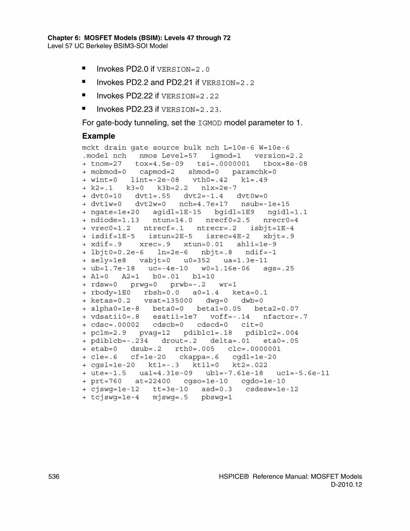
536 HSPICE® Reference Manual: MOSFET ModelsD-2010.12
Chapter 6: MOSFET Models (BSIM): Levels 47 through 72Level 57 UC Berkeley BSIM3-SOI Model
■ Invokes PD2.0 if VERSION=2.0■ Invokes PD2.2 and PD2.21 if VERSION=2.2■ Invokes PD2.22 if VERSION=2.22■ Invokes PD2.23 if VERSION=2.23.
For gate-body tunneling, set the IGMOD model parameter to 1.
Examplemckt drain gate source bulk nch L=10e-6 W=10e-6.model nch nmos Level=57 igmod=1 version=2.2+ tnom=27 tox=4.5e-09 tsi=.0000001 tbox=8e-08+ mobmod=0 capmod=2 shmod=0 paramchk=0+ wint=0 lint=-2e-08 vth0=.42 k1=.49+ k2=.1 k3=0 k3b=2.2 nlx=2e-7+ dvt0=10 dvt1=.55 dvt2=-1.4 dvt0w=0+ dvt1w=0 dvt2w=0 nch=4.7e+17 nsub=-1e+15+ ngate=1e+20 agidl=1E-15 bgidl=1E9 ngidl=1.1+ ndiode=1.13 ntun=14.0 nrecf0=2.5 nrecr0=4+ vrec0=1.2 ntrecf=.1 ntrecr=.2 isbjt=1E-4+ isdif=1E-5 istun=2E-5 isrec=4E-2 xbjt=.9+ xdif=.9 xrec=.9 xtun=0.01 ahli=1e-9+ lbjt0=0.2e-6 ln=2e-6 nbjt=.8 ndif=-1+ aely=1e8 vabjt=0 u0=352 ua=1.3e-11+ ub=1.7e-18 uc=-4e-10 w0=1.16e-06 ags=.25+ A1=0 A2=1 b0=.01 b1=10+ rdsw=0 prwg=0 prwb=-.2 wr=1+ rbody=1E0 rbsh=0.0 a0=1.4 keta=0.1+ ketas=0.2 vsat=135000 dwg=0 dwb=0+ alpha0=1e-8 beta0=0 beta1=0.05 beta2=0.07+ vdsatii0=.8 esatii=1e7 voff=-.14 nfactor=.7+ cdsc=.00002 cdscb=0 cdscd=0 cit=0+ pclm=2.9 pvag=12 pdiblc1=.18 pdiblc2=.004+ pdiblcb=-.234 drout=.2 delta=.01 eta0=.05+ etab=0 dsub=.2 rth0=.005 clc=.0000001+ cle=.6 cf=1e-20 ckappa=.6 cgdl=1e-20+ cgsl=1e-20 kt1=-.3 kt1l=0 kt2=.022+ ute=-1.5 ua1=4.31e-09 ub1=-7.61e-18 uc1=-5.6e-11+ prt=760 at=22400 cgso=1e-10 cgdo=1e-10+ cjswg=1e-12 tt=3e-10 asd=0.3 csdesw=1e-12+ tcjswg=1e-4 mjswg=.5 pbswg=1

HSPICE® Reference Manual: MOSFET Models 537D-2010.12
Chapter 6: MOSFET Models (BSIM): Levels 47 through 72Level 57 UC Berkeley BSIM3-SOI Model
UCB BSIMSOI3.1In addition to BSIMSOI3.0, the MOSFET Level 57 model also supports the UCB BSIMSOI3.1 model version, which includes the following new features that are not available in BSMISOI3.0.
Ideal Full-Depletion (FD) ModelingBSIMSOI3.0 supports the modeling of these two families of SOI MOSFETs with a SOIMOD switching model flag.■ SOIMOD=0 for partially depleted devices (PD).■ SOIMOD=1 for devices that tend to operate in a mixed mode of PD and FD.
V3.1 also provides an ideal full-depletion (FD) module (SOIMOD=2), not available in V3.0 to model FD SOI devices that literally exhibit no floating-body behavior. As in BSIMSOI3.0, the default SOIMOD value is 0 for BSIMSOI3.1.
The following physical modeling components, related to the internal SOI body node, are critical for accurately modeling PD SOI devices, but are not needed for the ideal FD module. Thus, for the ideal FD module, HSPICE ignores these components, which makes SOI MOSFET modeling much easier than for PD devices, or non-ideal FD devices.■ Source/Drain to body diode currents■ Source-Body-Drain parasitic BJT currents■ Impact ionization currents■ Gate-body direct currents■ Body-related capacitances.
Gate Resistance ModelingBSIMSOI3.1 uses the same gate resistance models as in the BSIM4 model with four options for various gate-resistance modeling topologies.
Table 165 BSIMSOI3.1 Gate Resistance Modeling Topologies
Name Unit Default Bin Description
NGCON - - N Number of gate contacts

538 HSPICE® Reference Manual: MOSFET ModelsD-2010.12
Chapter 6: MOSFET Models (BSIM): Levels 47 through 72Level 57 UC Berkeley BSIM3-SOI Model
Gate Resistance Equivalent CircuitRGATEMOD=0: No gate resistance (default)
RGATEMOD=1: Constant gate resistance
RGATEMOD - 0 N Gate resistance model selector■ RGATEMOD=0: No gate resistance■ RGATEMOD=1: Constant gate resistance■ RGATEMOD=2: Rii model with variable
resistance■ RGATEMOD=3: Rii model with two nodes
RSHG Ohm/Sq 0.1 N Gate electrode sheet resistance
XGL m 0 N Offset of the gate length due to variations in patterning
XGW m 0 N Distance from the gate contact to the channel edge in the W direction
XRCRG1 - 12 Y Parameter for distributed channel-resistance effect for intrinsic input resistance
XRCRG2 - 1 Y Parameter to account for the excess channel diffusion resistance for intrinsic input resistance
Table 165 BSIMSOI3.1 Gate Resistance Modeling Topologies
Name Unit Default Bin Description

HSPICE® Reference Manual: MOSFET Models 539D-2010.12
Chapter 6: MOSFET Models (BSIM): Levels 47 through 72Level 57 UC Berkeley BSIM3-SOI Model
RGATEMOD=2: variable resistance with Rii model
RGATEMOD=3: Rii model with two nodes
Rgeltd: (Poly) gate electrode resistance, bias independent.
Rii: Intrinsic input gate resistance, reflected to the gate from the intrinsic channel region. It is bias-dependent and a first-order non-quasi static model for RF and rapid transient MOSFET operations.
RgeltdRgeltd
Rgeltd+RiRgeltd+Ri
Rgelt
RiiCgso Cgd

540 HSPICE® Reference Manual: MOSFET ModelsD-2010.12
Chapter 6: MOSFET Models (BSIM): Levels 47 through 72Level 57 UC Berkeley BSIM3-SOI Model
Enhanced Binning CapabilityModel parameters for the following components are now binnable for better accuracy and scalability:■ Junction depth■ Gate-tunneling current■ Temperature dependence of threshold voltage, mobility, saturation velocity,
parasitic resistance, and diode currents.
Bug FixesThe BSIMSOI3.1 from UC Berkeley fixes the following bugs in the BSIMSOI3.0 model:■ The model now takes NSEG into account when calculating the gate-channel
tunneling current.■ The GMIN connecting gate and drain is now multiplied by 1e-6 to reduce
false leakage current.■ A swapping error in the source/drain overlap capacitance stamping.■ The bulk charge effect coefficient (AbulkCV) is now corrected for Qinv and its
derivatives in CAPMOD=2.
New Features in BSIMSOIv3.2Level 57 UC Berkeley BSIM3SOI ModelThe model selector, SoiMod, is an instance parameter and a model parameter. SoiMod will determine the operation of BSIMSOI.
If SoiMod=0 (default), the model equation is identical to the BSIMPD equation.
If SoiMod=1 (unified model for PD&FD) or SoiMod=2 (ideal FD), the following equations (FD module) are added on top of BSIMPD.

HSPICE® Reference Manual: MOSFET Models 541D-2010.12
Chapter 6: MOSFET Models (BSIM): Levels 47 through 72Level 57 UC Berkeley BSIM3-SOI Model
Here Nch is the channel doping concentration. NLX is the lateral non-uniform doping coefficient to account for the lateral non-uniform doping effect. VFBb is the backgate flatband voltage. Vth,FD is the threshold voltage at Vbs=Vbs0(phi=2ΦB). Vt is thermal voltage. K1 is the body effect coefficient.
If SoiMod=1, the lower bound of Vbs (SPICE solution) is set to Vbs0. If SoiMod=2, Vbs is pinned at Vbs0. Notice that there is no body node and body leakage/charge calculation in SoiMod=2.
The zero field body potential that will determine the transistor threshold voltage, Vbsmos,is then calculated by
BSIMSOIv3.2 Equation List Copyright© 2004, UC Berkeley
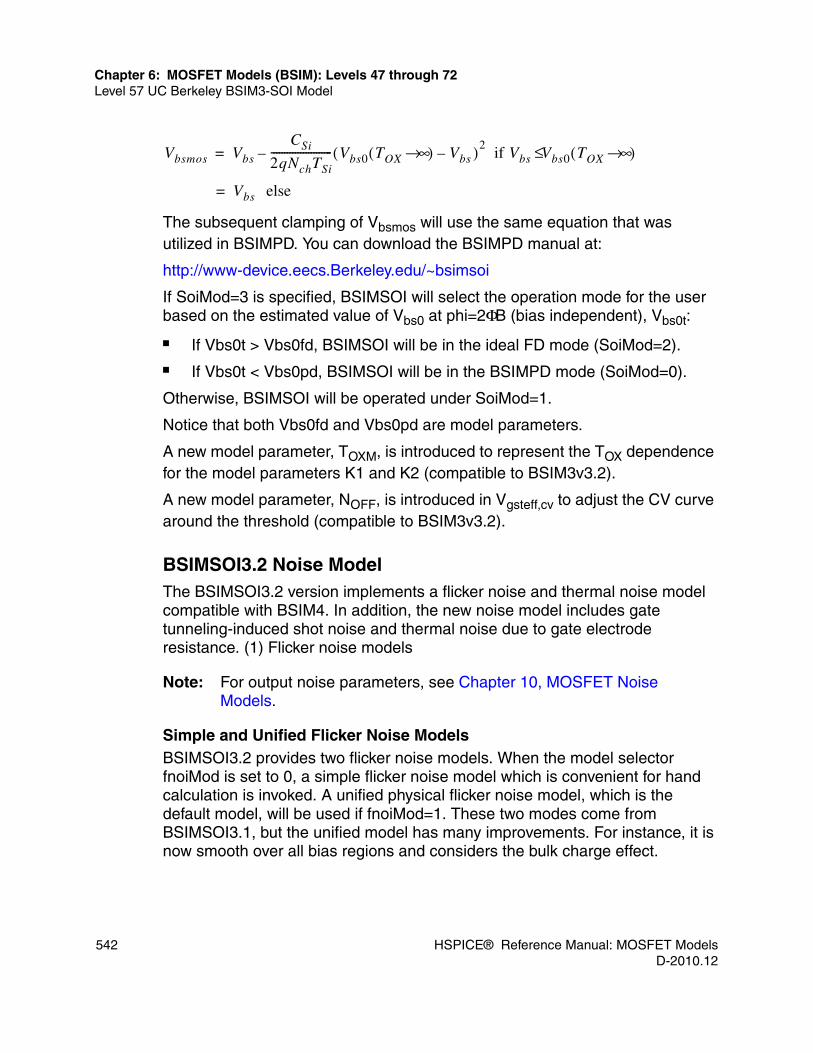
542 HSPICE® Reference Manual: MOSFET ModelsD-2010.12
Chapter 6: MOSFET Models (BSIM): Levels 47 through 72Level 57 UC Berkeley BSIM3-SOI Model
The subsequent clamping of Vbsmos will use the same equation that was utilized in BSIMPD. You can download the BSIMPD manual at:
http://www-device.eecs.Berkeley.edu/~bsimsoi
If SoiMod=3 is specified, BSIMSOI will select the operation mode for the user based on the estimated value of Vbs0 at phi=2ΦB (bias independent), Vbs0t:
■ If Vbs0t > Vbs0fd, BSIMSOI will be in the ideal FD mode (SoiMod=2).■ If Vbs0t < Vbs0pd, BSIMSOI will be in the BSIMPD mode (SoiMod=0).
Otherwise, BSIMSOI will be operated under SoiMod=1.
Notice that both Vbs0fd and Vbs0pd are model parameters.
A new model parameter, TOXM, is introduced to represent the TOX dependence for the model parameters K1 and K2 (compatible to BSIM3v3.2).
A new model parameter, NOFF, is introduced in Vgsteff,cv to adjust the CV curve around the threshold (compatible to BSIM3v3.2).
BSIMSOI3.2 Noise ModelThe BSIMSOI3.2 version implements a flicker noise and thermal noise model compatible with BSIM4. In addition, the new noise model includes gate tunneling-induced shot noise and thermal noise due to gate electrode resistance. (1) Flicker noise models
Note: For output noise parameters, see Chapter 10, MOSFET Noise Models.
Simple and Unified Flicker Noise ModelsBSIMSOI3.2 provides two flicker noise models. When the model selector fnoiMod is set to 0, a simple flicker noise model which is convenient for hand calculation is invoked. A unified physical flicker noise model, which is the default model, will be used if fnoiMod=1. These two modes come from BSIMSOI3.1, but the unified model has many improvements. For instance, it is now smooth over all bias regions and considers the bulk charge effect.
Vbsmos Vbs
CSi
2qNchTSi----------------------- Vbs0 TOX ∞→( ) Vbs )2
if Vbs Vbs0 TOX ∞→( )≤–(–=
Vbs else=

HSPICE® Reference Manual: MOSFET Models 543D-2010.12
Chapter 6: MOSFET Models (BSIM): Levels 47 through 72Level 57 UC Berkeley BSIM3-SOI Model
■ fnoiMOd = 0 (simple model)
The noise density is:■ fnoiMOd = 1 (unified model)
The physical mechanism for the flicker noise is trapping/de-trapping related charge fluctuation in oxide traps, which results in fluctuations of both mobile carrier numbers and mobility in the channel. The unified flicker noise model captures this physical process.
The noise density in inversion region is given by:
where μeff is the effective mobility at the given bias condition, and Leff and Weff are the effective length and width, respectively. The parameter N0 is the charge density at the source side given by:
The parameter N1 is the charge density at the source side given by:
N* is given by:
where CIT is a model parameter from DC IV and Cd is the depletion capacitance.ΔLclm is the channel length reduction due to channel length modulation and given by:
Sid f( )KfIds
af
COXLeff f2 ef
---------------------------=
N0
COXVgsteff
q-------------------------=
N1
CoxVgsteff
q------------------------ 1
AbulkVdseff
Vgsteff 2Vt+-----------------------------–⎝ ⎠
⎛ ⎞=
N* K TB
Cox Cd CIT+ +( )q2
------------------------------------------⋅=

544 HSPICE® Reference Manual: MOSFET ModelsD-2010.12
Chapter 6: MOSFET Models (BSIM): Levels 47 through 72Level 57 UC Berkeley BSIM3-SOI Model
In the subthreshold region, the noise density is written as:
The total flicker noise density is:
Thermal noise modelsThere are two channel thermal noise models in BSIMSOI3.2 version. One is the charge based model (default) similar to that used in BSIMSOI3.1. The other is the holistic model. These two models can be selected through the model selector tnoiMod.■ tnoiMod = 0 (charge based)
The noise current is given by:
where Rdsis the source/drain resistance, and the parameter NTNOI is introduced from more accurate fitting of short-channel devices. Qinv is the inversion channel charge computed from the capacitance models.■ tnoiMod = 1 (holistic)
In this thermal noise model, all the short-channel effects and velocity saturation effects incorporated in the IV model are automatically included, hence the name “holistic thermal noise model.” In addition, the amplification of the channel thermal noise through Gm and Gmbs as well as the induced- gate noise
ΔLclm Litl
Vds Vdseff–
Litl--------------------------- EM+
Esat-------------------------------------------log⋅=
Esat2VSAT
μeff------------------=
Sid subVt, f( )NOIA k TB Ids
2⋅ ⋅
WeffLeff fEF
N*2
1010⋅
------------------------------------------------------=
Sid f( )Sid inv, f( ) Sid insubvt, f( )×Sid inv, f( ) Sid insubvt, f( )+--------------------------------------------------------------=
id2 4kBTΔf
Leff2
------------------ NTNOI,
Rds μeff Qinv----------------------+
⋅=

HSPICE® Reference Manual: MOSFET Models 545D-2010.12
Chapter 6: MOSFET Models (BSIM): Levels 47 through 72Level 57 UC Berkeley BSIM3-SOI Model
with partial correlation to the channel thermal noise are all captured in the new “noise partition” model.
The noise voltage source partitioned to the source side is given by:
and the noise current source put in the channel region with gate and body amplification is given by:
where
Model Parameters in BSIMSOIv3.2 Table 166 Parameter Listing for BSIMSOIv3.2
Symbols Used in Equation
Symbol used in SPICE
Description Unit Default
SoiMod SoiMod SOI model selector (instance)SoiMOd=0 BSIMPDSoiMOd=1 Unified model for PD & FDSoiMod=2 ideal FDSoiMod=3 Auto selection by SIMSOI
- 0
TOXM toxm Gate oxide thickness used in extraction μ Tox
NOFF noff CV parameter for Vgesteff,cv - 1.0
Vbs0fd vbs0fd Upper bound of built-in potential lowering for ideal FD operation
V 0.0
vd2 4k TB θ2
moi
VdseffΔf
Ids-------------------⋅=
vd2 4k TB
VdseffΔf
Ids------------------- Gds[ βmoi Gm( Gmbs ) ]2
vd2 Gm( Gds Gmbs )2
++⋅–+⋅+=
θmoi RNOIB 1 T+ NOIB Leff
Vgsteff
EsatLeff
------------------⎝ ⎠⎛ ⎞
2⋅=
βmoi RNOIA 1 T+ NOIA Leff
Vgsteff
EsatLeff------------------⎝ ⎠
⎛ ⎞⋅2
=

546 HSPICE® Reference Manual: MOSFET ModelsD-2010.12
Chapter 6: MOSFET Models (BSIM): Levels 47 through 72Level 59 UC Berkeley BSIM3-SOI FD Model
Level 59 UC Berkeley BSIM3-SOI FD Model
The UC Berkeley SOI (BSIM3-SOI) Fully Depleted (FD) model is Level 59 in the Synopsys MOSFET models. For a description of this model, see the BSIM3SOI FD2.1 MOSFET MODEL User Manual, at:
http://www-device.eecs.berkeley.edu/~bsim3soi
The following sections discuss these topics:■ General Syntax for BSIM3-SOI FD Model■ Level 59 Model Parameters■ Level 59 Template Output
Vbs0fd vbs0fd Lowering bound of built- in potential lowering for ideal FD operation
V 0.5
fnoiMod fnoiMod Flicker noise model selector - 1
tnoiMod tnoiMod Thermal noise model selector - 0
NTNOI ntnoi Noise factor for short-channel devices for TNOIMOD=0 only
- 1.0
TNOIA tnoia Coefficient of channel-length dependence of total channel thermal noise
- 1.5
TNOIB tnoib Channel-length dependence parameter for channel thermal noise partitioning
- 3.5
RNOIA rnoia Thermal noise parameter 0.577
RNOIB rnoib Thermal noise parameter 0.37
Table 166 Parameter Listing for BSIMSOIv3.2
Symbols Used in Equation
Symbol used in SPICE
Description Unit Default
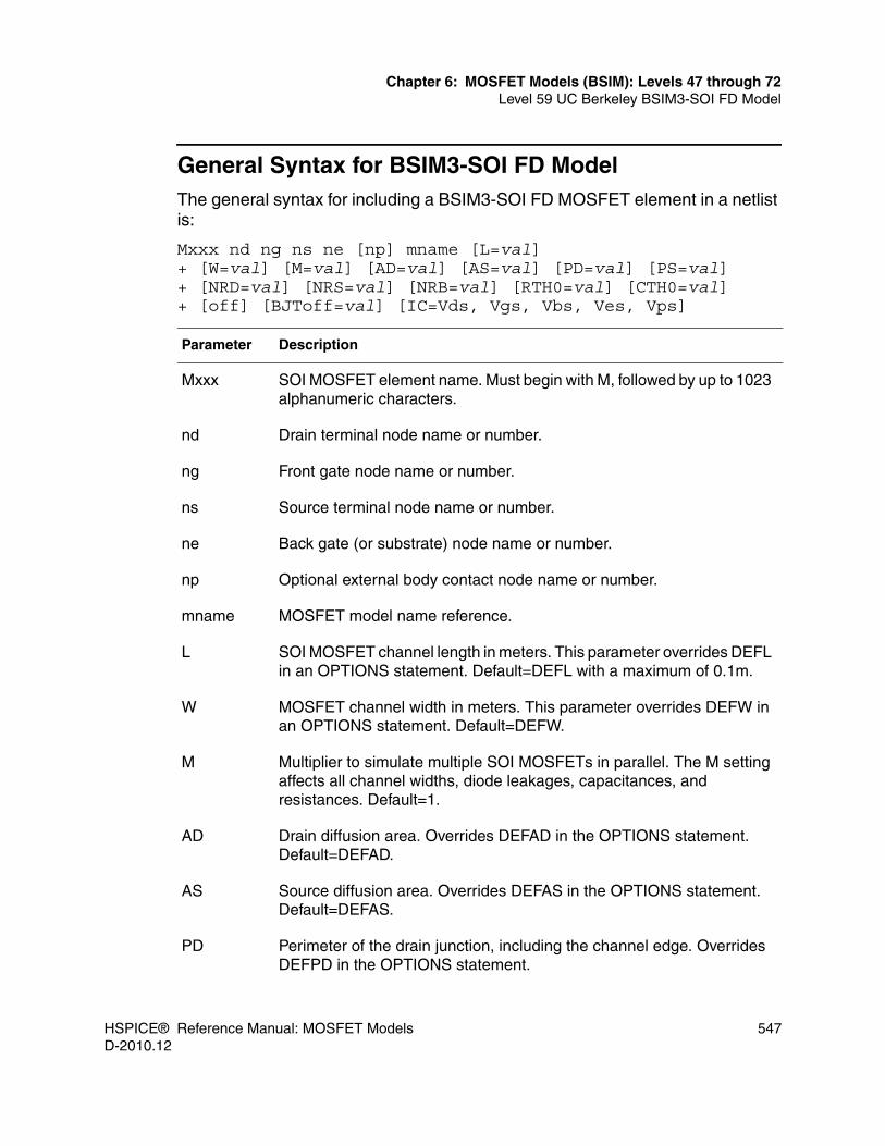
HSPICE® Reference Manual: MOSFET Models 547D-2010.12
Chapter 6: MOSFET Models (BSIM): Levels 47 through 72Level 59 UC Berkeley BSIM3-SOI FD Model
General Syntax for BSIM3-SOI FD Model The general syntax for including a BSIM3-SOI FD MOSFET element in a netlist is:
Mxxx nd ng ns ne [np] mname [L=val]+ [W=val] [M=val] [AD=val] [AS=val] [PD=val] [PS=val]+ [NRD=val] [NRS=val] [NRB=val] [RTH0=val] [CTH0=val]+ [off] [BJToff=val] [IC=Vds, Vgs, Vbs, Ves, Vps]
Parameter Description
Mxxx SOI MOSFET element name. Must begin with M, followed by up to 1023 alphanumeric characters.
nd Drain terminal node name or number.
ng Front gate node name or number.
ns Source terminal node name or number.
ne Back gate (or substrate) node name or number.
np Optional external body contact node name or number.
mname MOSFET model name reference.
L SOI MOSFET channel length in meters. This parameter overrides DEFL in an OPTIONS statement. Default=DEFL with a maximum of 0.1m.
W MOSFET channel width in meters. This parameter overrides DEFW in an OPTIONS statement. Default=DEFW.
M Multiplier to simulate multiple SOI MOSFETs in parallel. The M setting affects all channel widths, diode leakages, capacitances, and resistances. Default=1.
AD Drain diffusion area. Overrides DEFAD in the OPTIONS statement. Default=DEFAD.
AS Source diffusion area. Overrides DEFAS in the OPTIONS statement. Default=DEFAS.
PD Perimeter of the drain junction, including the channel edge. Overrides DEFPD in the OPTIONS statement.

548 HSPICE® Reference Manual: MOSFET ModelsD-2010.12
Chapter 6: MOSFET Models (BSIM): Levels 47 through 72Level 59 UC Berkeley BSIM3-SOI FD Model
Level 59 Model Parameters
PS Perimeter of the source junction, including the channel edge. Overrides DEFPS in the OPTIONS statement.
NRD Number of squares of drain diffusion for the drain series resistance. Overrides DEFNRD in the OPTIONS statement.
NRS Number of squares of source diffusion for the source series resistance. Overrides DEFNRS in the OPTIONS statement.
NRB Number of squares for the body series resistance.
RTH0 Thermal resistance per unit width:■ If you do not specify RTH0, simulation extracts it from the model
card.■ If you specify RTH0, it overrides RTH0 in the model card.
CTH0 Thermal capacitance per unit width■ If you do not specify CTH0, simulation extracts it from the model
card.■ If you specify CTH0, it overrides CTH0 in the model card.
OFF Sets the initial condition to OFF for this element in DC analysis.
BJTOFF Turns off BJT if equal to 1.
IC Initial guess in the order (drain, front gate, internal body, back gate, external voltage). (ignores Vps in a 4-terminal device) Simulation uses these settings if you specify UIC in the .TRAN statement. The .IC statement overrides them.
Table 167 Model Control Parameters, Level 59
Parameter Unit Default Description
CAPMOD - 2 Flag for the short channel capacitance model
Level - - Level 59 for BSIM3SOI
Parameter Description

HSPICE® Reference Manual: MOSFET Models 549D-2010.12
Chapter 6: MOSFET Models (BSIM): Levels 47 through 72Level 59 UC Berkeley BSIM3-SOI FD Model
MOBMOD - 1 Mobility model selector
NOIMOD - 1 Flag for the Noise model
SHMOD - 0 Flag for self-heating:■ 0=no self-heating■ 1=self-heating
Table 168 Process Parameters, Level 59
Parameter Unit Default Description
NCH 1/cm3 1.7e17 Channel doping concentration
NGATE 1/cm3 0 Poly gate doping concentration
NSUB 1/cm3 6.0e16 Substrate doping concentration
TBOX m 3.0e-7 Buried oxide thickness
TOX m 1.0e-8 Gate oxide thickness
TSI m 1.0e-17 Silicon film thickness
Table 169 DC Parameters, Level 59
Parameter Unit Default Description
A0 - 1.0 Bulk charge effect coefficient for the channel length
A1 1/V 0.0 First non-saturation effect parameter
A2 - 1.0 Second non-saturation effect parameter
ABP - 1.0 Coefficient of Abeff dependency on Vgst
ADICE0 - 1 DICE bulk charge factor
Table 167 Model Control Parameters, Level 59
Parameter Unit Default Description

550 HSPICE® Reference Manual: MOSFET ModelsD-2010.12
Chapter 6: MOSFET Models (BSIM): Levels 47 through 72Level 59 UC Berkeley BSIM3-SOI FD Model
AGIDL 1/W 0.0 GIDL constant
AGS 1/V 0.0 Gate bias coefficient of Abulk
AII 1/V 0.0 First Vdsatii parameter for the Leff dependence
ALPHA0 m/V 0.0 First parameter of the impact ionization current
ALPHA1 1/V 1.0 Second parameter of the impact ionization current
B0 m 0.0 Bulk charge effect coefficient for the channel width
B1 m 0.0 Width offset for the bulk charge effect
BGIDL V/m 0.0 GIDL exponential coefficient
BII m/V 0.0 Second Vdsatii parameter for the Leff dependence
CDSC F/m2 2.4e-4 Drain/source to the channel coupling capacitance
CDSCB F/m2 0 Body-bias sensitivity of cdsc
CDSCD F/m2 0 Drain-bias sensitivity of cdsc
CII - 0.0 First Vdsatii parameter for the Vds dependence
CIT F/m2 0.0 Interface trap capacitance
DELP V 0.02 Constant for limiting Vbseff to the surface potential
DELTA - 0.01 Effective Vds parameter
DII V -1.0 Second Vdsatii parameter for the Vds dependence
DROUT - 0.56 L dependence coefficient of the DIBL correction parameter in Rout
DSUB - 0.56 DIBL coefficient exponent
Table 169 DC Parameters, Level 59 (Continued)
Parameter Unit Default Description

HSPICE® Reference Manual: MOSFET Models 551D-2010.12
Chapter 6: MOSFET Models (BSIM): Levels 47 through 72Level 59 UC Berkeley BSIM3-SOI FD Model
DVBD0 V 0 First coefficient of the Vds 0 dependency on Leff
DVBD1 V 0 Second coefficient of the Vds 0 dependency on Leff
DVT0 - 2.2 First coefficient of the short-channel effect on Vth
DVT0W - 0 First coefficient of the narrow-width effect on Vth for a small channel length
DVT1 - 0.53 Second coefficient of the short-channel effect on Vth
DVT1W - 5.3e6 Second coefficient of the narrow-width effect on Vth for a small channel length
DVT2 1/V -0.032 Body-bias coefficient of the short-channel effect on Vth
DVT2W 1/V -0.032 Body-bias coefficient of the narrow width effect on Vth for small channel length
DWB m/V1/2 0.0 Coefficient of the substrate body bias dependence for Weff
DWG m/V 0.0 Coefficient of the gate dependence for Weff
EDL m 2e-6 Electron diffusion length
ETA0 - 0.08 DIBL coefficient in the subthreshold region
ETAB 1/V -0.07 Body-bias coefficient for the DIBL effect in the subthreshold region
ISBJT A/m2 1.0e-6 BJT injection saturation current
ISDIF A/m2 0 Body to source/drain injection saturation current
ISREC A/m2 1.0e-5 Recombination in the depletion saturation current
Table 169 DC Parameters, Level 59 (Continued)
Parameter Unit Default Description

552 HSPICE® Reference Manual: MOSFET ModelsD-2010.12
Chapter 6: MOSFET Models (BSIM): Levels 47 through 72Level 59 UC Berkeley BSIM3-SOI FD Model
ISTUN A/m2 0.0 Reverse tunneling saturation current
K1 V1/2 0.6 Coefficient for the first-order body effect
K2 - 0 Coefficient for the second-order body effect
K3 - 0 Narrow coefficient
K3B 1/V 0 Body-effect coefficient of k3
KB1 - 1 Coefficient of the Vbs 0 dependency on Vgbs
KB3 - 1 Coefficient of the Vbs0 dependency on Vgs at subthreshold region
KBJT1 m/V 0 Parasitic bipolar Early effect coefficient
KETA m -0.6 Body-bias coefficient of the bulk charge effect
LINT m 0.0 Length-offset fitting parameter from I-V without bias
MXC - -0.9 Fitting parameter for calculating Abeff
NDIODE - 1.0 Diode non-ideality factor
NFACTOR - 1 Subthreshold swing factor
NGIDL V 1.2 GIDL Vds enhancement coefficient
NLX m 1.74e-7 Lateral non-uniform doping parameter
NTUN - 10.0 Reverse tunneling non-ideality factor
PCLM - 1.3 Channel length modulation parameter
PDIBL1 - 0.39 First correction parameter for the DIBL effect of the output resistance
PDIBL2 - 0.0086 Second correction parameter for the DIBL effect of the output resistance
Table 169 DC Parameters, Level 59 (Continued)
Parameter Unit Default Description

HSPICE® Reference Manual: MOSFET Models 553D-2010.12
Chapter 6: MOSFET Models (BSIM): Levels 47 through 72Level 59 UC Berkeley BSIM3-SOI FD Model
PRWB 1/V1 0 Body effect coefficient of Rdsw
PRWG 1/V1/2 0 Gate bias effect coefficient of Rdsw
PVAG 0.0 Gate dependence of the Early voltage
RBODY ohm/m2 0.0 Intrinsic body contact sheet resistance
RBSH ohm/m2 0.0 Extrinsic body contact sheet resistance
RDSW 100 Parasitic resistance per unit width
RSH ohm/square 0.0 Source/drain sheet resistance in ohm per square
U0 cm2/(V-sec) NMOS-670PMOS-250
Mobility at Temp=Tnom
UA m/V 2.25e-9 First-order coefficient for mobility degradation
UB (m/V)2 5.87e-19 Second-order coefficient for mobility degradation
UC 1/V -0.0465 Body-effect coefficient for mobility degradation
VBSA V 0 Transition body voltage offset
VOFF v -0.08 Offset voltage in the subthreshold region for large W and L values
VSAT m/sec 8e4 Saturation velocity at Temp=Tnom
VTH0 v NMOS 0.7PMOS -0.7
Threshold voltage @ Vbs=0 for a long, wide device
W0 m 0 Narrow width parameter
WINT m 0.0 Width offset fitting parameter from I-V without bias
WR - 1 Width offset from Weff for calculating Rds
Table 169 DC Parameters, Level 59 (Continued)
Parameter Unit Default Description
Ω∗μmwr

554 HSPICE® Reference Manual: MOSFET ModelsD-2010.12
Chapter 6: MOSFET Models (BSIM): Levels 47 through 72Level 59 UC Berkeley BSIM3-SOI FD Model
Table 170 AC and Capacitance Parameters, Level 59
Parameter Unit Default Description
ASD V 0.3 Smoothing parameter for the source/drain bottom diffusion
CF F/m cal. Gate to source/drain fringing field capacitance
CGDL F/m 0.0 Lightly-doped drain-gate region overlap capacitance
CGDO F/m calculated Non-LDD region drain-gate overlap capacitance per channel length
CGEO F/m 0.0 Gate-substrate overlap capacitance per channel length
CGSL F/m 0.0 Lightly-doped source-gate region overlap capacitance
CGSO F/m calculated Non-LDD region source-gate overlap capacitance per channel length
CJSWG F/m2 1.e-10 Source/drain (gate side) sidewall junction capacitance per unit width (normalized to 100nm Tsi)
CKAPPA F/m 0.6 Coefficient for lightly-doped region overlap capacitance fringing field capacitance
CLC m 0.1e-7 Constant term for the short channel model
CLE - 0.0 Exponential term for the short channel model
CSDESW F/m 0.0 Source/drain sidewall fringing capacitance per unit length
CSDMIN V cal. Source/drain bottom diffusion minimum capacitance
DLC m lint Length offset fitting parameter for the gate charge
DWC m wint Width offset fitting parameter from C-V
MJSWG V 0.5 Source/drain (gate side) sidewall junction capacitance grading coefficient
PBSWG V 0.7 Built-in potential for the source/drain (gate side) sidewall junction capacitance

HSPICE® Reference Manual: MOSFET Models 555D-2010.12
Chapter 6: MOSFET Models (BSIM): Levels 47 through 72Level 59 UC Berkeley BSIM3-SOI FD Model
TT second 1ps Diffusion capacitance transit time coefficient
VSDFB V cal. Flatband voltage for the source/drain bottom diffusion capacitance
VSDTH V cal. Threshold voltage for the source/drain bottom diffusion capacitance
XPART - 0 Charge partitioning rate flag
Table 171 Temperature Parameters, Level 59
Parameter Unit Default Description
AT m/sec 3.3e4 Temperature coefficient for Ua
CTH0 moC/(W*s) 0 Normalized thermal capacity
KT1 V -0.11 Temperature coefficient for the threshold voltage
KT2 - 0.022 Body-bias coefficient for the temperature effect of the threshold voltage
KTIL V*m 0 Channel length dependence of the temperature coefficient for the threshold voltage
PRT -um 0 Temperature coefficient for Rdsw
RTH0 moC/W 0 Normalized thermal resistance
TNOM oC 25 Temperature at which simulation expects parameters
UA1 m/V 4.31e-9 Temperature coefficient for Ua
UB1 (m/V)2 -7.61e-18 Temperature coefficient for Ub
UC1 1/V -0.056 Temperature coefficient for Uc
Table 170 AC and Capacitance Parameters, Level 59
Parameter Unit Default Description
Ω

556 HSPICE® Reference Manual: MOSFET ModelsD-2010.12
Chapter 6: MOSFET Models (BSIM): Levels 47 through 72Level 60 UC Berkeley BSIM3-SOI DD Model
Note: BSIMFD refers the substrate to the silicon below the buried oxide, not to the well region in BSIM3. It calculates the backgate flatband voltage (Vfbb) and the parameters related to the bottom capacitance of the source/drain diffusion (Vsdth, Vsdfb, Csdmin).
■ Positive nsub means the same type of doping as the body.■ Negative nsub means opposite type of doping.
Level 59 Template OutputFor a list of output template parameters in the MOSFET models, and which parameters this model supports, see Table 4 on page 22.
Level 60 UC Berkeley BSIM3-SOI DD Model
The UC Berkeley SOI model (BSIM3SOI) supports Fully Depleted (FD), Partially Depleted (PD), and Dynamically Depleted (DD) SOI devices. BSIM3DD2.2 for DD SOI devices is Level 60 in the Synopsys MOSFET models. For a description of this model, see the BSIM3DD2.1 MOSFET MODEL User’s Manual, at
http://www-device.eecs.berkeley.edu/~bsim3
UTE - -1.5 Mobility temperature exponent
XBJT - 1 Power dependence of jbjt on the temperature
XDIF - XBJT Power dependence of jdif on the temperature
XREC - 1 Power dependence of jrec on the temperature
XTUN - 0 Power dependence of jtun on the temperature
Table 171 Temperature Parameters, Level 59
Parameter Unit Default Description

HSPICE® Reference Manual: MOSFET Models 557D-2010.12
Chapter 6: MOSFET Models (BSIM): Levels 47 through 72Level 60 UC Berkeley BSIM3-SOI DD Model
BSIM3DD2.1 includes many advanced concepts for dynamic and continuous transition between PD and FD operation. These concepts are collectively named Dynamic Depletion.
The following sections discuss these topics:■ Model Features■ General Syntax for BSIM3-SOI DD Model■ Level 60 BSIMSOI Model Parameters
Model Features■ Simulation applies dynamic depletion to both I-V and C-V. Tbox and Tsi
continuously scale the charge and drain current.■ Supports external body bias and backgate bias; a total of 6 nodes.■ Real floating body simulation in both I-V and C-V. Diode and C-V formulation
properly bind the body potential.■ Improved self-heating.■ Improved impact ionization current model.■ Various diode leakage components and parasitic bipolar current.■ Depletion charge model (EBCI) for better accuracy in predicting capacitive
coupling. The BSIM3v3 based model is also improved.■ Dynamic depletion can suit different requirements for SOI technologies.■ Single I-V expression as in BSIM3v3.1 to assure continuities of Ids, Gds,
Gm and their derivatives for all bias conditions.
General Syntax for BSIM3-SOI DD ModelThe general syntax for a BSIM3SOI MOSFET element in a netlist is:
Mxxx nd ng ns ne [np] mname [L=val] [W=val] [M=val]+ [AD=val] [AS=val] [PD=val] [PS=val][NRD=val] [NRS=val]+ [NRB=val] [RTHO=val] [CTHO=val] [off] [BJToff=val]+ [IC=Vds, Vgs, Vbs, Ves, Vps] [SOIQ0=val]

558 HSPICE® Reference Manual: MOSFET ModelsD-2010.12
Chapter 6: MOSFET Models (BSIM): Levels 47 through 72Level 60 UC Berkeley BSIM3-SOI DD Model
Parameter Description
Mxxx SOI MOSFET element name. Must begin with M, followed by up to 1023 alphanumeric characters.
nd Drain terminal node name or number.
ng Front gate node name or number.
ns Source terminal node name or number.
ne Back gate (or Substrate) node name or number.
np External body contact node name or number.
mname MOSFET model name reference.
L SOI MOSFET channel length in meters. This parameter overrides DEFL in an .OPTION statement. Default=DEFL with a maximum of 0.1m.
W SOI MOSFET channel width in meters. This parameter overrides DEFW in an .OPTION statement. Default=DEFW with a maximum of 0.1m.
M Multiplier to simulate multiple SOI MOSFETs in parallel. The M setting affects all channel widths, diode leakages, capacitances, and resistances. Default=1.
AD Drain diffusion area. Overrides DEFAD in the .OPTION statement: Default=DEFAD
AS Source diffusion area. Overrides DEFAS in the .OPTION statement: Default=DEFAS
PD Perimeter of the drain junction, including the channel edge. Overrides DEFPD in the .OPTION statement.
PS Perimeter of the source junction, including the channel edge. Overrides DEFPS in the .OPTION statement.
NRD Number of squares of the drain diffusion for the drain series resistance. Overrides DEFNRD in the .OPTION statement.

HSPICE® Reference Manual: MOSFET Models 559D-2010.12
Chapter 6: MOSFET Models (BSIM): Levels 47 through 72Level 60 UC Berkeley BSIM3-SOI DD Model
NRS Number of squares of the source diffusion for the source series resistance. Overrides DEFNRS in the.OPTION statement.
NRB Number of squares for the body series resistance.
RDC Additional drain resistance due to the contact resistance in units of ohms. This value overrides the RDC setting in the model specification. Default=0.0.
RSC Additional source resistance due to the contact resistance in units of ohms. This value overrides the RDC setting in the model specification. Default=0.0.
RTHO Thermal resistance per unit width:■ If you do not specify RTHO, simulation extracts it from the model
card.■ If you specify RTHO, it overrides RTHO in the model card.
CTHO Thermal capacitance per unit width:■ If you do not specify CTHO, simulation extracts it from the model
card.■ If you specify CTHO, it overrides CTHO in the model card.
OFF Sets the initial condition to OFF for this element in DC analysis.
BJTOFF Turns off BJT if equal to 1.
IC Initial guess in the order (drain, front gate, internal body, back gate, external voltage). Simulation ignores Vps in a 4-terminal device. Use these settings if you specify UIC in the .TRAN statement. The .IC statement overrides it.
SOIQ0 Floating body charge initialization. This parameter is set for the BQI algorithm of a floating body node.
Parameter Description

560 HSPICE® Reference Manual: MOSFET ModelsD-2010.12
Chapter 6: MOSFET Models (BSIM): Levels 47 through 72Level 60 UC Berkeley BSIM3-SOI DD Model
Level 60 BSIMSOI Model ParametersTable 172 Control Parameters, Level 60
SPICESymbol
Description Unit Default Notes SeeTable 177
shMod Flag for self-heating■ 0=no self-heating■ 1=self-heating
- 0
mobMod Mobility model selector - 1 -
capMod Flag for the short channel capacitance model - 2 nI-1
noiMod Flag for the noise model - 1 -
Table 173 Process Parameters, Level 60
SPICESymbol
Description Unit Default Notes SeeTable 177
Tsi Silicon film thickness m 10-7 -
Tbox Buried oxide thickness m 3x10⁻⁷ -
Tox Gate oxide thickness m 1x10⁻⁸ -
Nch Channel doping concentration 1/cm3 1.7x10¹⁷ -
Nsub Substrate doping concentration 1/cm3 6x10¹⁶ nI-2
ngate Poly gate doping concentration 1/cm3 0 -
Table 174 DC Parameters, Level 60
SPICESymbol
Description Unit Default Notes SeeTable 177
vth0 Threshold voltage @ Vbs=0 for the long and wide device
V 0.7 for N-0.7 for P
nI-3

HSPICE® Reference Manual: MOSFET Models 561D-2010.12
Chapter 6: MOSFET Models (BSIM): Levels 47 through 72Level 60 UC Berkeley BSIM3-SOI DD Model
k1 First order body effect coefficient V1/2 0.5 -
k2 Second order body-effect coefficient - 0 -
k3 Narrow width coefficient - 0 -
k3b Body-effect coefficient of k3 1/V 0 -
Vbsa Transition body voltage offset V 0 -
delp Constant for limiting Vbseff to fs V 0.02 -
Kb1 Coefficient of Vbs0 dependency on Ves - 1 -
Dvbd0 First coefficient of Vbs0, Leff dependency V 0 -
Dvbd1 Second coefficient of Vbs0, Leff dependency
V 0 -
w0 Narrow width parameter m 0 -
nlx Lateral non-uniform doping parameter m 1.74e-7 -
dvt0 First coefficient of the short-channel effect on Vth
- 2.2 -
dvt1 Second coefficient of the short-channel Vth effect
- 0.53 -
dvt2 Body-bias coefficient of the short-channel Vth effect
1/V -0.032 -
dvt0w First coefficient of the narrow-width effect on Vth for a small channel length
- 0 -
dvt1w Second coefficient of the narrow-width effect on Vth for a small channel length
- 5.3e6 -
dvt2w Body-bias coefficient of the narrow-width effect on Vth for a small channel length
1/V -0.032 -
Table 174 DC Parameters, Level 60
SPICESymbol
Description Unit Default Notes SeeTable 177

562 HSPICE® Reference Manual: MOSFET ModelsD-2010.12
Chapter 6: MOSFET Models (BSIM): Levels 47 through 72Level 60 UC Berkeley BSIM3-SOI DD Model
u0 Mobility at Temp=Tnom■ NMOSFET■ PMOSFET
cm2/(V-sec) 670
250
-
ua First-order mobility degradation coefficient m/V 2.25e-9 -
ub Second-order mobility degradation coefficient
(m/V)2 5.9e-19 -
uc Body-effect of the mobility degradation coefficient
1/V -.0465 -
vsat Saturation velocity at Temp=Tnom m/sec 8e4 -
a0 Bulk charge effect coefficient for the channel length
- 1.0 -
ags Gate bias coefficient of Abulk 1/V 0.0 -
b0 Bulk charge effect coefficient for the channel width
m 0.0 -
b1 Bulk charge effect width offset m 0.0 -
keta Body-bias coefficient of the bulk charge effect
m -0.6 -
Abp Coefficient of the Abeff dependency on Vgst
- 1.0 -
mxc Fitting parameter for calculating Abeff - -0.9 -
adice0 DICE bulk charge factor - 1 -
A1 First non-saturation effect parameter 1/V 0.0 -
A2 Second non-saturation effect parameter 0 1.0 -
rdsw Parasitic resistance per unit width Ω-mmWr 100 -
Table 174 DC Parameters, Level 60
SPICESymbol
Description Unit Default Notes SeeTable 177

HSPICE® Reference Manual: MOSFET Models 563D-2010.12
Chapter 6: MOSFET Models (BSIM): Levels 47 through 72Level 60 UC Berkeley BSIM3-SOI DD Model
prwb Body-effect coefficient of Rdsw 1/V 0 -
prwg Gate bias effect coefficient of Rdsw 1/V1/2 0 -
wr Width offset from Weff for calculating Rds - 1 -
wint Width offset fitting parameter of I-V without bias
m 0.0 -
lint Length offset fitting parameter of I-V without bias
m 0.0 -
dwg Coefficient of the gate dependence of Weff m/V 0.0
dwb Coefficient, substrate body bias dependence, Weff
m/V1/2 0.0
voff Offset voltage in the subthreshold region for large W and L values
V -0.08 -
nfactor Subthreshold swing factor - 1 -
eta0 DIBL coefficient in the subthreshold region - 0.08 -
etab Body-bias coefficient for subthreshold DIBL effect
1/V -0.07 -
dsub DIBL coefficient exponent - 0.56 -
cit Interface trap capacitance F/m2 0.0 -
cdsc Drain/Source to the channel coupling capacitance
F/m2 2.4e-4 -
cdscb Body-bias sensitivity of Cdsc F/m2 0 -
cdscd Drain-bias sensitivity of Cdsc F/m2 0 -
pclm Channel length modulation parameter - 1.3 -
Table 174 DC Parameters, Level 60
SPICESymbol
Description Unit Default Notes SeeTable 177

564 HSPICE® Reference Manual: MOSFET ModelsD-2010.12
Chapter 6: MOSFET Models (BSIM): Levels 47 through 72Level 60 UC Berkeley BSIM3-SOI DD Model
pdibl1 Correction parameter for the DIBL effect of the first output resistance
- .39 -
pdibl2 Correction parameter for the DIBL effect of the second output resistance
- 0.086 -
drout L dependence coefficient of the DIBL correction parameter in Rout
- 0.56 -
pvag Gate dependence of the Early voltage - 0.0 -
delta Effective Vds parameter - 0.01 -
aii First Vdsatii parameter for the Leff dependence
1/V 0.0 -
bii Second Vdsatii parameter for the Leff dependence
m/V 0.0 -
cii First Vdsatii parameter for the Vds dependence
- 0.0 -
dii Second Vdsatii parameter for the Vds dependence
V -1.0 -
alpha0 First parameter of the impact ionization current
m/V 0.0 -
alpha1 Second parameter of the impact ionization current
1/V 1.0 -
beta0 Third parameter of the impact ionization current
V 30 -
Agidl GIDL constant Ω-1 0.0 -
Bgidl GIDL exponential coefficient V/m 0.0 -
Ngidl GIDL Vds enhancement coefficient V 1.2 -
Table 174 DC Parameters, Level 60
SPICESymbol
Description Unit Default Notes SeeTable 177

HSPICE® Reference Manual: MOSFET Models 565D-2010.12
Chapter 6: MOSFET Models (BSIM): Levels 47 through 72Level 60 UC Berkeley BSIM3-SOI DD Model
ntun Reverse tunneling non-ideality factor - 10.0 -
Ndiode Diode non-ideality factor - 1.0 -
Isbjt BJT injection saturation current A/m2 1e-6 -
Isdif Body to source/drain injection saturation current
A/m2 0.0 -
Isrec Recombination in the depletion saturation current
A/m2 1e-5 -
Istun Reverse tunneling saturation current A/m2 0.0 -
Edl Electron diffusion length m 2e-6 -
Kbjt1 Parasitic bipolar early effect coefficient m/V 0 -
Rbody Intrinsic body contact sheet resistance ohm/m2 0.0 -
Rbsh Extrinsic body contact sheet resistance ohm/m2 0.0 -
rsh Source drain sheet resistance in ohm per square
Ω/square 0.0 -
Table 175 AC and Capacitance Parameters, Level 60
SPICESymbol
Description Unit Default SeeTable 177
xpart Charge partitioning rate flag - 0
cgso Non-LDD region source-gate overlap capacitance per channel length
F/m calculated nC-1
cgdo Non-LDD region drain-gate overlap capacitance per channel length
F/m calculated nC-2
cgeo Gate substrate overlap capacitance per unit channel length
F/m 0.0 -
Table 174 DC Parameters, Level 60
SPICESymbol
Description Unit Default Notes SeeTable 177

566 HSPICE® Reference Manual: MOSFET ModelsD-2010.12
Chapter 6: MOSFET Models (BSIM): Levels 47 through 72Level 60 UC Berkeley BSIM3-SOI DD Model
cjswg Source/Drain (gate side) sidewall junction
Capacitance per unit width (normalized to 100nm Tsi)
F/m2 1e-10 -
pbswg Built-in potential for the Source/Drain (gate side) sidewall junction capacitance
V .7 -
mjswg Grading coefficient for the Source/Drain (gate side) sidewall junction capacitance
V 0.5 -
tt Coefficient for the diffusion capacitance transit time
second 1ps -
vsdfb Flatband voltage for the source/drain bottom diffusion capacitance
V calculated nC-3
vsdth Threshold voltage for the source/drain bottom diffusion capacitance
V calculated nC-4
csdmin Minimum capacitance of the source/drain bottom diffusion
V calculated nC-5
asd Smoothing parameter for the source/drain bottom diffusion
- 0.3 -
csdesw Source/drain sidewall fringing capacitance per unit length
F/m 0.0 -
cgs1 Overlap capacitance for the lightly-doped source-gate region
F/m 0.0 -
cgd1 Overlap capacitance for the lightly-doped drain-gate region
F/m 0.0 -
ckappa Coefficient of the fringing field capacitance for the overlap capacitance in the lightly-doped region
F/m 0.6 -
Table 175 AC and Capacitance Parameters, Level 60
SPICESymbol
Description Unit Default SeeTable 177

HSPICE® Reference Manual: MOSFET Models 567D-2010.12
Chapter 6: MOSFET Models (BSIM): Levels 47 through 72Level 60 UC Berkeley BSIM3-SOI DD Model
cf Fringing field capacitance for the gate-to-source/drain
F/m calculated nC-6
clc Constant term for the short-channel mode m 0.1x10⁻⁷ -
cle Exponential term for the short-channel mode none 0.0 -
dlc Length offset fitting parameter from C-V m lint -
dwc Width offset fitting parameter from C-V m wint -
Table 176 Temperature Parameters, Level 60
SPICESymbol
Description Unit Default SeeTable 177
tnom Temperature at which simulation expects parameters
oC 27 -
ute Mobility temperature exponent none -1.5 -
kt1 Temperature coefficient for the threshold voltage
V -0.11 -
kt11 Channel length dependence of the temperature coefficient for the threshold voltage
V*m 0.0
kt2 Body-bias coefficient of the Vth temperature effect
none 0.022 -
ua1 Temperature coefficient for Ua m/V 4.31e-9 -
ub1 Temperature coefficient for Ub (m/V)2 -7.61e-18 -
uc1 Temperature coefficient for Uc 1/V -.056 nT-1
at Temperature coefficient for the saturation velocity
m/sec 3.3e4 -
Table 175 AC and Capacitance Parameters, Level 60
SPICESymbol
Description Unit Default SeeTable 177

568 HSPICE® Reference Manual: MOSFET ModelsD-2010.12
Chapter 6: MOSFET Models (BSIM): Levels 47 through 72Level 60 UC Berkeley BSIM3-SOI DD Model
cth0 Normalized thermal capacity moC/(W*sec) 0 -
prt Temperature coefficient for Rdsw Ω-μm 0 -
rth0 Normalized thermal resistance moC/W 0 -
xbjt Power dependence of jbjt on the temperature
none 2 -
xdif Power dependence of jdif on the temperature
none 2 -
xrec Power dependence of jrec on the temperature
none 20 -
xtun Power dependence of jtun on the temperature
none 0 -
Table 177 MOSFET Level 60 Model Parameter Notes
Note Explanation
nI-1 Capmod 0 and 1 do not calculate the dynamic depletion. Therefore, ddMod does not work with capmod.
nI-2 BSIMSOI refers to a substrate of the silicon below the buried oxide, not the well region in BSIM3. It calculates the backgate flatband voltage (Vfbb) and the parameters related to the source/drain diffusion bottom capacitance (Vsdth, Vsdfb, Csdmin).
■ Positive nsub is the same type of doping as the body.■ Negative nsub is the opposite type of doping.
nC-1 If you do not specify cgso, simulation calculates it:■ if you specify dlc greater than 0, then cgso=pl=(dlc*cox)-cgs1■ if the previously-calculated cgso<0, then cgso=0■ else cgso=0.6*Tsi*cox
nC-2 Calculates Cgdo similar to Csdo
Table 176 Temperature Parameters, Level 60
SPICESymbol
Description Unit Default SeeTable 177

HSPICE® Reference Manual: MOSFET Models 569D-2010.12
Chapter 6: MOSFET Models (BSIM): Levels 47 through 72Level 65 SSIMSOI Model
Level 65 SSIMSOI Model
Level 65 is a surface-potential, charge-based, and partially depleted SOI MOSFET model developed by Motorola semiconductor.
The following sections discuss these topics:■ Using Level 65 with Synopsys Simulators■ General Syntax for SSIMSOI
nC-3 If nsub is positive, then:
else:
nC-4 If nsub is positive, then:
else:
nC-5
nC-6 If you do not specify cf, then simulation calculates it:
nT-1 For mobmod=1 and 2, the unit is m/V2. Default is -5.6E-11. For mobmod=3, the unit is 1/V and the default is -0.056.
Table 177 MOSFET Level 60 Model Parameter Notes
Note Explanation
VsdfbkTq
------10
20nsub⋅
ni ni⋅----------------------------
⎝ ⎠⎜ ⎟⎛ ⎞
0.3–log–= VsdfbkTq
------ 1020
nsub----------
⎝ ⎠⎜ ⎟⎛ ⎞
0.3+log–=
φsd 2kTq
------nsub
ni----------⎝
⎛⎠⎞ ϒsd
5.753x10¹²–
nsub
Cbox---------------------------------------------=,log= Vsdth Vsdfb φsd ϒsd φsd+ +=
φsd 2kTq
------nsub
ni----------–⎝
⎛⎠⎞ ϒsd
5.753x10¹²–
nsub–
Cbox------------------------------------------------=,log= Vsdth Vsdfb φsd– ϒsd– φsd+=
Xsddep
2ε siφsd
q nsub 106⋅
-------------------------------- Csddep
ε si
Xsddep---------------- Csdmin
CsddepCbox
Csddep Cbox+----------------------------------=,=,=
CF2ε ox
π-----------1n 1
4x10⁷–
Tox-----------------+
⎝ ⎠⎜ ⎟⎛ ⎞
=

570 HSPICE® Reference Manual: MOSFET ModelsD-2010.12
Chapter 6: MOSFET Models (BSIM): Levels 47 through 72Level 65 SSIMSOI Model
Using Level 65 with Synopsys SimulatorsTo simulate using the SSIMSOI model:
1. Set LEVEL=65 to identify the model as the SSIMSOI model.
2. Set the correct simulator room temperature.
The default room temperature is 25C in Synopsys circuit simulators, but is 27C in most other simulators. When comparing to other simulators, use TEMP 27 or .OPTION TNOM=27 to set the simulation temperature to 27
in the netlist.
3. Set DTEMP on the element line.
You can use DTEMP with this model to increase the temperature of individual elements, relative to the circuit temperature. If you do not specify DTEMP, simulation extracts TRISE from the model card. If you do specify DTEMP, it overrides TRISE in the model card.
General Syntax for SSIMSOIMxxx nd ng ns ne [np] mname [L=val] [W=val]
+ [M=val] [AD=val] [AS=val] [PD=val] [PS=val]+ [BODYTYPE=val] [IGATE=val] [AB=val] [PB=val] [LXB=val]+ [WXB=val] [LPE=val] [DTEMP=val]
Parameter Description
Mxxx SSIMSOI element name. Must begin with M, followed by up to 1023 alphanumeric characters.
nd Drain terminal node name or number.
ng Front gate node name or number.
ns Source terminal node name or number.
ne Back gate (or Substrate) node name or number.
np External body contact node name or number.
mname SSIMSOI model name reference.

HSPICE® Reference Manual: MOSFET Models 571D-2010.12
Chapter 6: MOSFET Models (BSIM): Levels 47 through 72Level 65 SSIMSOI Model
L SSIMSOI channel length in meters. Default is 5.0 um.
W SSIMSOI channel width in meters. Default is 5.0 um.
M Multiplier to simulate multiple SSIMSOIs in parallel. Default=1.
AD Drain diffusion area. Default=0.
AS Source diffusion area. Default=0.
PD Drain diffusion perimeter. Default=0.
PS Source diffusion perimeter. Default=0.
BODYTYPE Flag to choose floating(0) or Tgate(2). Default=0.
IGATE Flag to turn on/off(0/1) gate current calculations. Default=1.
AB Body diffusion area. Default=0.
PB Body diffusion perimeter (Body Contacted). Default=0.
LXB Extrinsic Gate Length (Body Contacted). Default=0.
WXB Extrinsic Gate Width (Body Contacted). Default=0.
LPE Flag to turn on/off lpe-related parasitics.
DTEMP Increases the temperature.
Table 178 SSIMSOI Model intrinsic Parameters (Geometry Modifiers and Threshold Voltage)
Name Parameter Units Default
tox Gate oxide thickness. Angstrom 250
tbox Back oxide thickness. Angstrom 250
tsi Silicon film thickness. cm 0.2e-4
Parameter Description

572 HSPICE® Reference Manual: MOSFET ModelsD-2010.12
Chapter 6: MOSFET Models (BSIM): Levels 47 through 72Level 65 SSIMSOI Model
vth0 Linear region vth, reference (large) MOSFET, Vbs=0 v 0.8 (nmos)-0.8 (pmos)
tcv Temperature coefficient of threshold voltage. 1/K 0
vfb Reference (large) MOSFET flatband voltage v calc
tcvfb Temperature coefficient of flatband voltage 1/K
ng Poly gate doping density 1/cm3
ngf Gate oxide fixed charge density 1/cm2 0
pbias Length modifier (use with odif) micron 0
dlivcv Length modified for capacitance model micron 0
odif Outdiffusion of s/d under gate micron 0
odifs Outdiffusion of s under gate (asymmetric) micron oidf
abias Width modifier micron 0
lldd Ldd spacer width micron 0
lg2ct Distance from contact to poly edge micron 1.0
dbias Diffusion resistor processing bias micron 0
nfs Fast surface state density 1/V-cm2 0
n1 Surface region doping density 1/cm3 5.0e16
n2 Bulk region doping density 1/cm3 2.0e16
wbrk Depth of surface region micron 0.2
vfbll Length dependence parameter of vth0 0
vfble Exponent for length dependence of vth0 -1
Table 178 SSIMSOI Model intrinsic Parameters (Geometry Modifiers and Threshold Voltage)
Name Parameter Units Default

HSPICE® Reference Manual: MOSFET Models 573D-2010.12
Chapter 6: MOSFET Models (BSIM): Levels 47 through 72Level 65 SSIMSOI Model
vfbwl Width dependence parameter of vth0 0
vfbwe Exponent for width dependence of vth0 -1
dphii Norm. error in phi at extro. Vth0 0
cs1ll I-dependence parameter of n1 0
cs1le Exponent for I-dependence of n1 -1
cs2ll I-dependence parameter of n2 0
cs2le Exponent for I-dependence of n2 -1
cs1wl W-dependence parameter of n1 0
cs1we Exponent for w-dependence of n1 -1
cs2wl W-dependence parameter of n2 0
cs2we Exponent for w-dependence of n2 -1
dibll I-dependence parameter of dibl 0
dible Exponent for I-dependence of dibl -2
gp1 Bulk charge coefficient 1.744
gp2 Bulk charge coefficient 1/V 0.8364
shrink Linear size reduction % 0
shrink2 Modified areal size reduction % 0
Table 178 SSIMSOI Model intrinsic Parameters (Geometry Modifiers and Threshold Voltage)
Name Parameter Units Default

574 HSPICE® Reference Manual: MOSFET ModelsD-2010.12
Chapter 6: MOSFET Models (BSIM): Levels 47 through 72Level 65 SSIMSOI Model
Table 179 SSIMSOI Model Intrinsic Parameters (Mobility and Saturation, Output Conductance)
Name Parameter Units Default
ubref Mobility parameter cm2/V-s 700 (nmos)300 (pmos)
ubred Mobility filed reduction factor (cm/V)egvexp 100
eavfac Effective field coefficient 0.5
eavfwl Width dependence of eavfac 0.0
eavfwe Exponent of width dependence of eavfac -2.0
eavexp Exponent of mobility field function 1.0
ubvds Drain dependence of eff. field 0.5
vsat Channel carrier saturation velocity cm/sec 1.0e-7
esat0 Vsat divisor, velocity field model 2
esat1 Divisor, carrier velocity at sat. 1
lc00 Mult. For channel length modulation 0.2
lc01 Length dependence of lc00 1/micron 0
lc1 Bias dependence of channel length modulation 1/V 0
wlmod Mult. for channel width modulation 0
dv2 Par. for lin/sat transition region 0.05
dv3 Length dependence of dv2 0
exb Temperature exponent of ubref 1.5
Table 180 SSIMSOI Model Parasitic Parameters
Name Parameter Units Default
aimp0 Impact ionization parameter 0

HSPICE® Reference Manual: MOSFET Models 575D-2010.12
Chapter 6: MOSFET Models (BSIM): Levels 47 through 72Level 65 SSIMSOI Model
aimpl Length dependence of aimp0 micron 0
aimpw Width dependence of aimp0 micron 0
aimpt Temperature dependence of aimp0 1/K 0
bimp0 Exponent for impact ionization 1/V 28.0
bimpl Length dependence of bimp0 micron 0
bimp2 Width dependence of bimp0 micron 0
fsat1 Bias dependence of impact ionization 1/V 0
onkink Voltage adjustment for onset of the kink V 0
gtundeltox Intrinsic region delta tox (electrical vs physical) angstrom (off)
gtundtoxovl S/D overlap region delta tox (electrical vs physical) angstrom (off)
gtunstoxovl S overlap region delta tox (asymmetric) angstrom gundtoxovl
gtunwdep Accumulation 2-D fringing parameter micron 0
gtunecbm ECB effective mass 0.4
gtunecba ECB fitting parameter 0.6
gtunecbb ECB barrier height V 3.1
gtunecbbo ECB barrier height V 3.1
gtunhvbm HWB effective mass 0.3
gtunhvba HVB fitting parameter 1.0
gtunhvbb HVB barrier height V 4.5
gtunhvbbo HVB barrier height V 4.5
gtunevbeg EVB energy bandgap V 1.12
Table 180 SSIMSOI Model Parasitic Parameters
Name Parameter Units Default
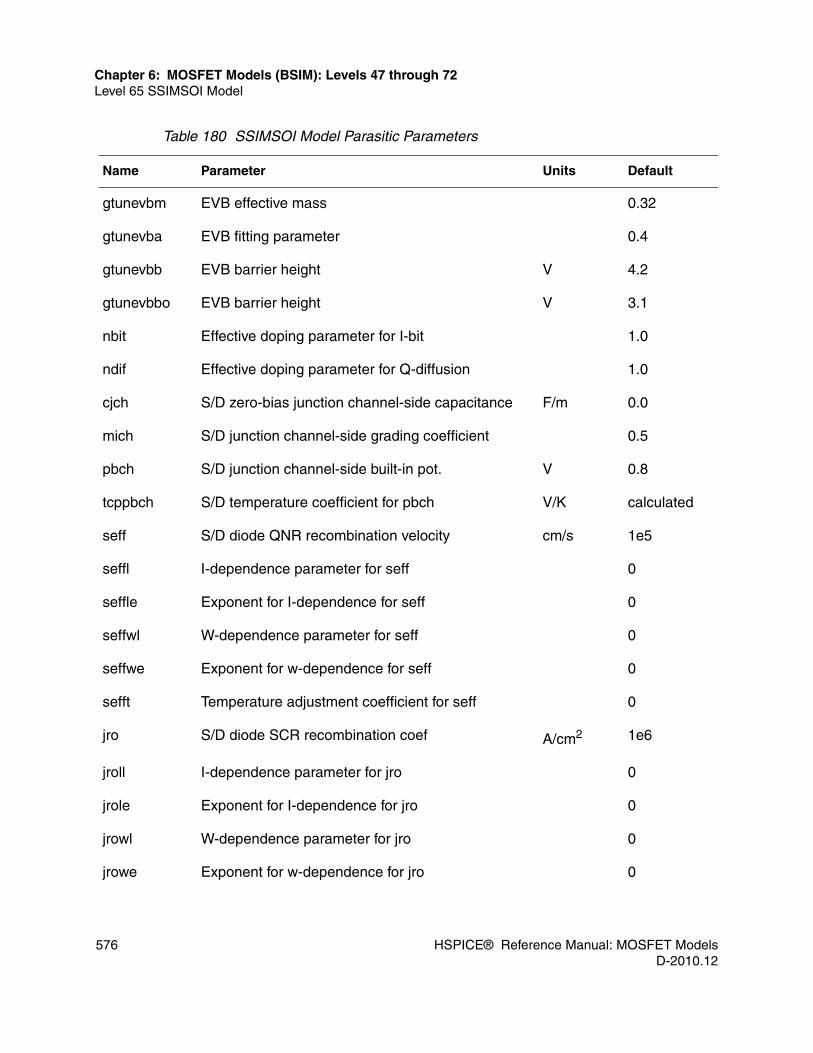
576 HSPICE® Reference Manual: MOSFET ModelsD-2010.12
Chapter 6: MOSFET Models (BSIM): Levels 47 through 72Level 65 SSIMSOI Model
gtunevbm EVB effective mass 0.32
gtunevba EVB fitting parameter 0.4
gtunevbb EVB barrier height V 4.2
gtunevbbo EVB barrier height V 3.1
nbit Effective doping parameter for I-bit 1.0
ndif Effective doping parameter for Q-diffusion 1.0
cjch S/D zero-bias junction channel-side capacitance F/m 0.0
mich S/D junction channel-side grading coefficient 0.5
pbch S/D junction channel-side built-in pot. V 0.8
tcppbch S/D temperature coefficient for pbch V/K calculated
seff S/D diode QNR recombination velocity cm/s 1e5
seffl I-dependence parameter for seff 0
seffle Exponent for I-dependence for seff 0
seffwl W-dependence parameter for seff 0
seffwe Exponent for w-dependence for seff 0
sefft Temperature adjustment coefficient for seff 0
jro S/D diode SCR recombination coef A/cm2 1e6
jroll I-dependence parameter for jro 0
jrole Exponent for I-dependence for jro 0
jrowl W-dependence parameter for jro 0
jrowe Exponent for w-dependence for jro 0
Table 180 SSIMSOI Model Parasitic Parameters
Name Parameter Units Default
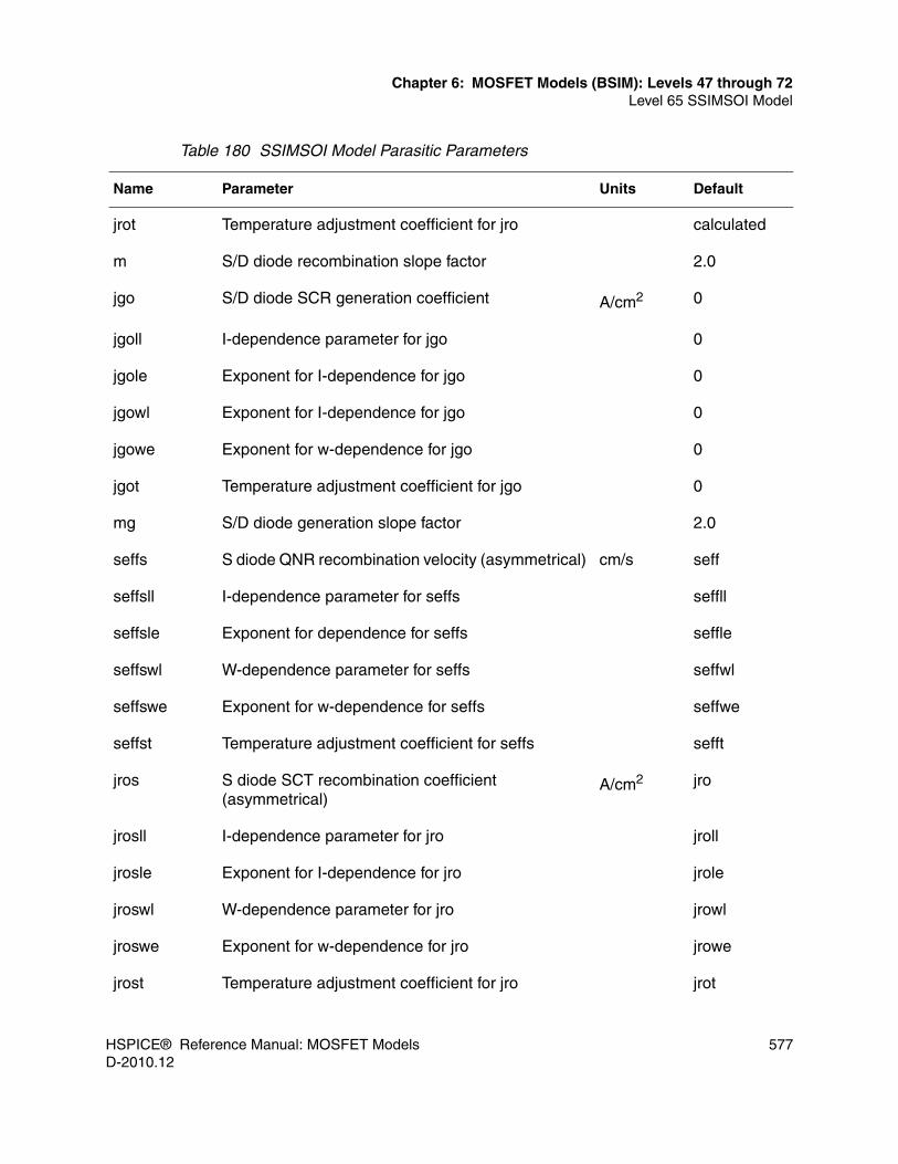
HSPICE® Reference Manual: MOSFET Models 577D-2010.12
Chapter 6: MOSFET Models (BSIM): Levels 47 through 72Level 65 SSIMSOI Model
jrot Temperature adjustment coefficient for jro calculated
m S/D diode recombination slope factor 2.0
jgo S/D diode SCR generation coefficient A/cm2 0
jgoll I-dependence parameter for jgo 0
jgole Exponent for I-dependence for jgo 0
jgowl Exponent for I-dependence for jgo 0
jgowe Exponent for w-dependence for jgo 0
jgot Temperature adjustment coefficient for jgo 0
mg S/D diode generation slope factor 2.0
seffs S diode QNR recombination velocity (asymmetrical) cm/s seff
seffsll I-dependence parameter for seffs seffll
seffsle Exponent for dependence for seffs seffle
seffswl W-dependence parameter for seffs seffwl
seffswe Exponent for w-dependence for seffs seffwe
seffst Temperature adjustment coefficient for seffs sefft
jros S diode SCT recombination coefficient (asymmetrical)
A/cm2 jro
jrosll I-dependence parameter for jro jroll
jrosle Exponent for I-dependence for jro jrole
jroswl W-dependence parameter for jro jrowl
jroswe Exponent for w-dependence for jro jrowe
jrost Temperature adjustment coefficient for jro jrot
Table 180 SSIMSOI Model Parasitic Parameters
Name Parameter Units Default

578 HSPICE® Reference Manual: MOSFET ModelsD-2010.12
Chapter 6: MOSFET Models (BSIM): Levels 47 through 72Level 65 SSIMSOI Model
ms S diode recombination slope factor (asymmetrical) m
jgos S diode SCR generation coefficient (asymmetrical) A/cm2 jgo
jgosll I-dependence parameter for jgo jgoll
jgosle Exponent for I-dependence for jgo jgole
jgoswl W-dependence parameter for jgo jgowl
jgoswe Exponent for w-dependence for jgo jgowe
jgost Temperature adjustment coefficient for jgo jgot
mgs S diode generation slope factor mg
gidla GIDL pre-exponential parameter A/m (off)
gidlb GIDL exponential parameter m/V 3.0e9
gidlc GIDL bulk-dependence parameter V3 8.0
gidle GIDL bandgap V calculated
gidlt GIDL temperature-dependence parameter calculated
gisla GISL pre-exponential parameter A/m gidla
gislb GISL exponential parameter m/V gidlb
gislc GISL bulk-dependence parameter V3 gidlc
gisle GISL bandgap V gidle
gislt GISL temperature-dependence parameter gidlt
rshmin Sheet res. of s/d-gate overlap ohm/sq 0
tcmin Temperature coefficient for rshmin 1/K 0
rshmins Sheet res. of s-gate overlap (asymmetrical) ohm/sq rshmin
Table 180 SSIMSOI Model Parasitic Parameters
Name Parameter Units Default

HSPICE® Reference Manual: MOSFET Models 579D-2010.12
Chapter 6: MOSFET Models (BSIM): Levels 47 through 72Level 65 SSIMSOI Model
tcmins Temperature coefficient for rshims (asymmetrical) 1/K tcmin
rshpls Sheet res. of heavily doped S/D ohm/sq 0
tcpls Temperature coefficient for rshpls 1/K 0
rshbody Sheet res. of intrinsic body ohm/sq 3000
rshbodyext Sheet res. of extrinsic body ohm/sq 3000
tcbody Temperature coefficient for rshbody and rshbodyext 1/K 0
cfr Gate to S/D fringing capacitance F/micron 0
cfrs Gate to s-fringing capacitance (asymmetrical) F/micron cfr
foc Bias dependence of overlap capacitance 1.0
voc Bias dependence of overlap capacitance V 0
cfrb Gate to body overlap capacitance F/micron 0
cfrbox Back-gate to S/D fringing capacitance F/micron 0
odifact S/D active diffusion micron 0
odifbc Body contact diffusion micron 0
ccp Contact-to-poly capacitance F/micron 0
ccpr Ccp error in RCE netlist F/micron 0
ccc Contact-to-contact capacitance F/micron 0
cccr Ccc error in RCE netlists F/micron 0
ccx Contact-to-soisub capacitance F/micron 0
cpx Poly-to-soisub capacitance F/micron 0
wfr Additional contact width micron 0
Table 180 SSIMSOI Model Parasitic Parameters
Name Parameter Units Default

580 HSPICE® Reference Manual: MOSFET ModelsD-2010.12
Chapter 6: MOSFET Models (BSIM): Levels 47 through 72Level 66 HSPICE HVMOS Model
Level 66 HSPICE HVMOS Model
The HSPICE Level 66 model is Synopsys’ proprietary model for high-voltage CMOS integrated circuits design and simulation. It is accurate in modeling the high-voltage device physics and robust in SPICE simulation. It is designed for various high-voltage CMOS processes, technology nodes, and device structures, including both widely-employed LDMOS (Laterally Diffused MOS) and EDMOS (Extended Drain MOS) transistors that may have any field plate oxide layer which helps the drain engineering. In addition, applications can be whole power management ICs such as switch power supply controllers, flash memory, hot-swap chips, and chips used in the automotive and medical industries.
This HSPICE HVMOS model is fully supported by Synopsys’ parameter extraction tool, Aurora, and it has been widely adopted for production by many semiconductor companies and major foundries.
The model has been developed based on BSIM4, with high accuracy in geometrical, bias, and temperature scaling. It explicitly and accurately considers the following physical effects: independent bias-dependent drain/source resistances, quasi-saturation, self-heating, Gm fall-off in the saturation region, symmetric and asymmetrical source and drain structures, and many other high-voltage operation-related unique device behaviors.
For the details and usage, contact the Synopsys support teams.
General Syntax for the Level 66 ModelThe general syntax for including a LEVEL 66 model element in a netlist is:
nlev Flicker noise equation level 0
kf Flicker noise coefficient 0.0
af Flicker noise exponent 1.0
cexp Flicker noise cox exponent 1.0
fexp Flicker noise frequency exponent 1.0
Table 180 SSIMSOI Model Parasitic Parameters
Name Parameter Units Default

HSPICE® Reference Manual: MOSFET Models 581D-2010.12
Chapter 6: MOSFET Models (BSIM): Levels 47 through 72Level 66 HSPICE HVMOS Model
Mxxx nd ng ns [nb] mname [L=val] [W=val] [M=val]+ [AD=val] [AS=val] [PD=val] [PS=val] + [RGATEMOD=val] [RBODYMOD=val]+ [ACNQSMOD=val] [GEOMOD=val] [RGEOMOD=val]+ [NRS=val] [NRD=val] [RBPB=val] [RBPD=val]+ [RBPS=val] [RBSB=val]+ [MIN=val] [RDC=val] [RSC=val] [DELVTO=val]+ [MULU0=val] [DELK1=val]+ [DELTOX=val] [OFF] [IC=Vds, Vgs, Vbs]+ [WNFLAG=val]
The following table lists and describe the HVMOS Level 66 general parameters.
Note: For Level 66, the following list only presents the HSPICE proprietary model parameters, while the rest are the same as BSIM4.
Table 181 General Parameters for the Level 66 Model
Parameter Description
ACNQSMOD AC small-signal NQS model selector.
AD Drain diffusion area.
AS Source diffusion area.
DELK1 Shift in body bias coefficient (K1).
DELNFCT Shift in subthreshold swing factor (NFACTOR).
DELTOX Shift in gate electrical and physical oxide thickness (TOXE and TOXP). That is, the difference between the electrical and physical gate oxide/insulator thicknesses.
DELVTO (DELVT0)
Shift in the VTH0 zero-bias threshold voltage.
GEOMOD Geometry-dependent parasitics model selector—specifies how the end S/D diffusions connect.
IC Initial guess in the order
L MOSFET channel length in meters.

582 HSPICE® Reference Manual: MOSFET ModelsD-2010.12
Chapter 6: MOSFET Models (BSIM): Levels 47 through 72Level 66 HSPICE HVMOS Model
MIN Whether to minimize the number of drain or source diffusions for even-number fingered device.
mname MOSFET model name reference.
MULU0 Low-field mobility (U0) multiplier.
nb Bulk terminal node name.
nd Drain terminal node name.
NF Number of device fingers.
ng Gate terminal node name.
NRD Number of drain diffusion squares.
NRS Number of source diffusion squares.
ns Source terminal node name.
OFF Sets the initial condition to OFF in DC analysis.
PD Perimeter of the drain junction:■ If PERMOD=0, it excludes the gate edge.■ Otherwise, it includes the gate edge.
PS Perimeter of the source junction:■ If PERMOD=0, it excludes the gate edge.■ Otherwise, it includes the gate edge.
RBDB Resistance connected between dbNode and bNode.
RBODYMOD Substrate resistance network model selector.
RBPB Resistance connected between bNodePrime and bNode.
RBPD Resistance connected between bNodePrime and dbNode.
RBPS Resistance connected between bNodePrime and sbNode.
Table 181 General Parameters for the Level 66 Model (Continued)
Parameter Description

HSPICE® Reference Manual: MOSFET Models 583D-2010.12
Chapter 6: MOSFET Models (BSIM): Levels 47 through 72Level 70 BSIMSOI4.x Model Parameters
Note: To print the substrate current when using the Level=66 model, you need to turn on the instance parameter RBODYMOD to output the substrate current. For example:MN VD VG VS VB nmod w=1 l=0.2 RBODYMOD=1
HSPICE prints mobility parameters for Level 66 and Level 68.
Level 70 BSIMSOI4.x Model Parameters
The UC Berkeley SOI model (BSIMSOI4.0) addresses several issues in modeling sub-0.13 micron CMOS/SOI high-speed and RF circuit simulations. Many inputs from the Compact Model Council (CMC) meetings were incorporated into the model. This model is fully backward compatible with its previous 3.X versions. For a description of this model, see the BSIMSOI4.0 MOSFET Model User’s Manual at
http://www-device.eecs.berkeley.edu/~bsimsoi/get.html
RBSB Resistance connected between sbNode and bNode.
RDC Drain contact resistance for per-finger device.
RGATEMOD Gate resistance model selector.
RGEOMOD Source/drain diffusion resistance and contact model selector—specifies the end S/D contact type: point wide or merged) and how to compute the S/D parasitics resistance.
RSC Source contact resistance for per-finger device.
TRNQSMOD Transient NQS model selector.
W MOSFET channel width in meters.
WNFLAG Turn on to select bin model based on width per NF for multi-finger devices.
Table 181 General Parameters for the Level 66 Model (Continued)
Parameter Description

584 HSPICE® Reference Manual: MOSFET ModelsD-2010.12
Chapter 6: MOSFET Models (BSIM): Levels 47 through 72Level 70 BSIMSOI4.x Model Parameters
The BSIMSOI4.0 model provides the following major improvements and additions over the BSIMSOI3.2 model:■ A scalable stress effect model for process induced stress effect; device
performance thus becomes a function of the active area geometry and the location of the device in the active area.
■ An asymmetric current/capacitance model S/D diode and asymmetric S/D resistance.
■ An improved GIDL model with BSIM4 GIDL compatibility.■ Noise model improvements, such as:
• Improved width/length dependence on flicker noise
• SPICE2 thermal noise model is introduced as TNOIMOD=2 with parameter NTNOI that adjusts the magnitude of the noise density
• Body contact resistance induced thermal noise
• Thermal noise induced by the body resistance network
• Shot noises induced by Ibs and Ibd separated■ A two resistance body resistance network introduced for RF simulation.■ Threshold voltage model enhancement, such as:
• Long-channel DIBL effect model added
• Channel-length dependence of body effect improved■ Drain-induced threshold shift (DITS) model introduced in output
conductance.■ Improved model accuracy in moderate inversion region with BSIM4
compatible Vgsteff.■ Multi-finger device with instance parameter NF.■ A new instance parameter AGBCPD to improve gate current for body contact.■ A new instance parameter DELVTO representing threshold voltage variation.■ Instance FRBODY is both an instance and a model parameter.
The following sections discuss these topics:■ BSIMSOI4.3.1 Update■ BSIMSOI4.2, 4.3 Updates■ BSIMOI4.1 Update

HSPICE® Reference Manual: MOSFET Models 585D-2010.12
Chapter 6: MOSFET Models (BSIM): Levels 47 through 72Level 70 BSIMSOI4.x Model Parameters
■ General Syntax for BSIMSOI4.x Model■ BSIMOI4.x Model Parameters■ Parameter Range Limit for BSIM4SOI4 Level 70
BSIMSOI4.3.1 UpdateIn BSIMSOI4.3.1 the following updates are added:
1. The temperature derivative expressions are greatly improved.
2. Bugfixes related to mtrlMod=1 are incorporated.
3. Thermal noise NF issue is fixed in SOI4.3.1.
For a description of this model, see the BSIMSOI4..3.1 MOSFET Model User's Manual athttp://www-device.eecs.berkeley.edu/~bsimsoi/get.html
BSIMSOI4.2, 4.3 UpdatesIn BSIMSOI versions 4.2 and 4.3, the following features were added:
1. Some bugs such as charge derivative issues are fixed in version 4.2.
2. The charge derivative issues in v4.2 and earlier versions are greatly improved in version 4.3.
3. Many expressions and derivatives are greatly improved in version 4.3, such as GISL.
4. A model parameter BSOIUPDATE=0|1 has been added using a flag to control thermal noise nf fix for v. 4.3. Its default value is 0, providing “No fix” for backward compatibility. Setting BSOIUPDATE=1 turns on the HSPICE thermal noise nf fix.
BSIMOI4.1 UpdateIn BSIMSOI4.1, the following features were added:■ A new material model (mtrlMod)■ Asymmetric GIDL/GISL model and new GIDL/GISL model (gidlMod)■ A new impact-ionization current model

586 HSPICE® Reference Manual: MOSFET ModelsD-2010.12
Chapter 6: MOSFET Models (BSIM): Levels 47 through 72Level 70 BSIMSOI4.x Model Parameters
■ An improved Coulombic scattering model for high k/metal gate■ An improved body-contact model to characterize the opposite-type gate
■ A new Vbi model to simplify the parameter extraction
■ A new VgsteffCV model for C-V, which is similar to Vgsteff in I-V■ A new gate current component in body contact region■ An improved DITS model with more flexibility and better fit
For a description of this model, see the BSIMSOI4.1 MOSFET Model User's Manual at http://www-device.eecs.berkeley.edu/~bsimsoi/get.html
Model parameter range limits for SSIMSOI4 are listed in Table 194 on page 607.
General Syntax for BSIMSOI4.x ModelThe general syntax for a BSIMSOI4.0 MOSFET element in a netlist is:
MXXX nd ng ns ne [np] [nb] [nT] mname [L=val] [W=val]+ [M=val] [AD=val] [AS=val] [PD=val] [PS=val] [NRD=val] + [NRS=val] [NRB=val] [RTH0=val] [CTH0=val] [NBC=val] + [NSEG=val] [PDBCP=val] [PSBCP=val] [AGBCP=val] [AEBCP=val] + [VBSUSR=val] [DELTOX=val] [TNODEOUT] [off] [FRBODY=val] + [BJTOFF=val] [IC=vds, vgs, vbs, ves, vps] [dtemp=val] + [soimod=val] [rgatemod=val] [nf=val] [sa=val] [sb=val] + [sd=val] [rbdb=val] [rbsb=val] [delvto=val] [agbcpd=val] + [rbodymod=val] [mulu0=val] [SOIQ0=val] + [DELSVAT=val] [MULSVAT=val]
Parameter Description
Mxxx SOI MOSFET element name. Must begin with M, followed by up to 1023 alphanumeric characters.
nd Drain terminal node name or number.
ng Front gate node name or number.
ns Source terminal node name or number.
ne Back gate (or Substrate) node name or number.
Δ

HSPICE® Reference Manual: MOSFET Models 587D-2010.12
Chapter 6: MOSFET Models (BSIM): Levels 47 through 72Level 70 BSIMSOI4.x Model Parameters
np External body contact node name or number. If 'body node' is to be checked in a .biaschk command, use keyword 'np' as in the BSIM3 SOI model.
nb Internal body node name or number.
nT Temperature node name or number.
mname SOI MOSFET model name reference.
L SOI MOSFET channel length in meters. The default is 5e-6.
W SOI MOSFET channel width in meters. The default is 5e-6.
M Multiplier to simulate multiple SOI MOSFETs in parallel. The M setting affects all channel widths, diode leakages, capacitances, and resistances. The default is 1.
AD Drain diffusion area. The default is 0.
AS Source diffusion area. The default is 0.
PD Perimeter of the drain junction, including the channel edge. The default is 0.
PS Perimeter of the source junction, including the channel edge. The default is 0.
NRD Number of squares of drain diffusion for the drain series resistance. The default is 1.
NRS Number of squares of source diffusion for the source series resistance. The default is 1.
NRB Number of squares for the body series resistance. The default is 1.
FRBODY Coefficient of the distributed body resistance effects.■ If FRBODY is not specified, it’s extracted from the model card■ If FRBODY is specified, it overrides FRBODY in the model card
RTH0 Thermal resistance per unit width.■ If RTH0 is not specified, it’s extracted from the model card■ If RTH0 is specified, it overrides RTH0 in the model card
CTH0 Thermal capacitance per unit width.■ If CTH0 is not specified, it’s extracted from the model card■ If CTH0 is specified, it overrides RTH0 in the model card
NBC Number of body contact isolation edge. The default is 0
NSEG Number of segments for partitioning the channel width. The default is 1
PDBCP Parasitic perimeter length for the body contact at the drain side. The default is 0
Parameter Description

588 HSPICE® Reference Manual: MOSFET ModelsD-2010.12
Chapter 6: MOSFET Models (BSIM): Levels 47 through 72Level 70 BSIMSOI4.x Model Parameters
PSBCP Parasitic perimeter length for the body contact at the source side. The default is 0
AGBCP Parasitic gate-to-body overlap area for the body contact. The default is 0
AEBCP Parasitic body to substrate overlap area for the body contact. The default is 0
VBSUSR Optional initial value of Vbs that you specify for transient analysis.
DELTOX Shift in gate oxide thickness (TOX), that is, the difference between the electrical and physical gate oxide/insulator thickness. The default is 0
TNODEOUT Temperature node flag indicating the use of the T node. If you do not set TNODEOUT, you can specify four nodes for a device to float the body. Specifying five nodes implies that the fifth node is the external body contact node with a body resistance between the internal and external terminals. This configuration applies to a distributed body resistance simulation.If you set TNODEOUT, simulation interprets the last node as the temperature node. You can specify five nodes to float the device. Specifying six nodes implies body contact. Seven nodes is a body-contacted case with a accessible internal body node. You can use the temperature node to simulate thermal coupling.
OFF Sets the initial condition to OFF for this element in DC analysis.
BJTOFF Turns off BJT if equal to 1.
IC Initial guess in the order (drain, front gate, internal body, back gate, external voltage). Simulation ignores Vps in a 4-terminal device. Use these settings if you specify UIC in the .TRAN statement. The .IC statement overrides it.
DTEMP Increase in temperature. The default is 0.
SOIMOD SOI model selector.■ If SOIMOD is not specified, it’s extracted from the model card■ If SOIMOD is specified, it overrides SOIMOD in the model card
RGATEMOD Gate resistance model selector.■ If RGATEMOD is not specified, it’s extracted from the model card■ If RGATEMOD is specified, it overrides RGATEMOD in the model card
NF Number of fingers. The default is 1.
SA Distance between OD edge to poly from one side. The default is 0.
SB Distance between OD edge to poly from another side. The default is 0.
SD Distance between neighboring fingers. The default is 0.
Parameter Description

HSPICE® Reference Manual: MOSFET Models 589D-2010.12
Chapter 6: MOSFET Models (BSIM): Levels 47 through 72Level 70 BSIMSOI4.x Model Parameters
BSIMOI4.x Model ParametersThe following tables list and describe the BSIMSOI4.0 model parameters.■ Control Parameters, Level 70■ Process Parameters, Level 70■ DC Parameters, Level 70■ Gate-to-body Tunneling Parameters, Level 70■ AC and Capacitance Parameters, Level 70■ Temperature Parameters, Level 70■ Built-in Potential Lowering Model Parameters, Level 70■ Gate Resistance Parameters, Level 70■ Body Resistance Parameters, Level 70■ Noise Parameters, Level 70
RBDB Resistance between dbNode and bNode.■ If RBDB is not specified, it’s extracted from the model card■ If RBDB is specified, it overrides RBDB in the model card
RBSB Resistance between sbNode and bNode.■ If RBSB is not specified, it’s extracted from the model card■ If RBSB is specified, it overrides RBSB in the model card
DELVTO Zero bias threshold voltage variation. The default is 0.
AGBCPD Parasitic gate to body overlap area for body contact in DC. The default is 0.
RBODYMOD Body resistance model selector.■ If RBODYMOD is not specified, it’s extracted from the model card■ If RBODYMOD is specified, it overrides RBODYMOD in the model card
MULU0 Low-field mobility (U0) multiplier(U0_eff = MULU0*U0), the default is 1.0
SOIQ0 Floating body charge initialization. This parameter is set for the BQI algorithm of a floating body node.
DELSVAT Shift in Saturation velocity (VSAT).
MULSVAT Scaling factor of Saturation velocity (VSAT), the default is 1.0.
Parameter Description

590 HSPICE® Reference Manual: MOSFET ModelsD-2010.12
Chapter 6: MOSFET Models (BSIM): Levels 47 through 72Level 70 BSIMSOI4.x Model Parameters
■ Stress Model Parameters, Level 70■ Avalanche Impact Ionization Parameters, Level 70
Table 182 Control Parameters, Level 70
Parameter Description Unit Default Bin
VERSION Mode version number - 4.3.1 N
BSOIUPDATE Flag for fixing thermal noise NF issue in versions 4.0-4.3■ 0 = Does not fix noise NF issue■ 1 = Fixes noise NF issue
0 N
SHMOD Flag for self-heating■ 0=no self-heating■ 1=self-heating
- 0 N
MOBMOD Mobility model selector - 1 N
CAPMOD Flag for the short channel capacitance modelCAPMOD=2 and 3 are supported, CAPMOD=0 and 1 are not supported.
- 2 N
IGCMOD Gate to channel tunneling current model selector - 0 N
RDSMOD Bias-dependent S/D resistance model selector - 0 N
Table 183 Process Parameters, Level 70
Parameter Description Unit Default Bin
TSI1 Silicon film thickness m 1e-7 N
TBOX Buried oxide thickness m 3e-7 N
TOX Gate oxide thickness m 1e-8 N
TOXM Oxide thickness used in extraction m TOX N
NCH Channel doping concentration cm-3 1.7e17 Y
NSUB2 Substrate doping concentration cm-3 6e16 Y

HSPICE® Reference Manual: MOSFET Models 591D-2010.12
Chapter 6: MOSFET Models (BSIM): Levels 47 through 72Level 70 BSIMSOI4.x Model Parameters
NGATE Poly gate doping concentration cm-3 0 Y
1. In modern SOI technology, source/drain extension or LDD are commonly used. As a result, the source/drain junction depth (XJ) can be different from the silicon film thickness (TSI). By default, if XJ is not given, it is set to TSI. XJ is not allowed to be greater than TSI.
2. BSIMSOI4.0 refers the substrate to the silicon below the buried oxide (not to the well region in BSIM4) to calculate the backgate flatband voltage (Vfbb) and the parameters related to the source/drain diffusion bottom capacitance (Vsdth, Vsdfb, and Csdmin)– Positive NSUB means the same type of doping as the body– Negative NSUB means the opposite type of doping.
Table 184 DC Parameters, Level 70
Parameter Description Unit Default Bin
VTH0(VTO)
Threshold voltage @ Vbs=0 for the long and wide device
V 0.7 for N-0.7 for P
Y
K1 First order body effect coefficient V-1/2 0.6 Y
K1W1 First body effect width dependent parameter m 0 Y
K1W2 Second body effect width dependent parameter m 0 Y
K2 Second order body-effect coefficient - 0 Y
K3 Narrow width coefficient - 0 Y
K3B Body effect coefficient V-1 0 Y
KB1 Backgate body charge coefficient - 1 Y
W0 Narrow width parameter m 0 Y
LPE0(NLX)
Lateral non-uniform doping parameter m 1.74e-7 Y
LPEB Lateral non-uniform doping effect for body bias m 0 Y
DVT0 First coefficient of the short-channel effect on Vth - 2.2 Y
Table 183 Process Parameters, Level 70
Parameter Description Unit Default Bin

592 HSPICE® Reference Manual: MOSFET ModelsD-2010.12
Chapter 6: MOSFET Models (BSIM): Levels 47 through 72Level 70 BSIMSOI4.x Model Parameters
DVT1 Second coefficient of the short-channel Vth effect - 0.53 Y
DVT2 Body-bias coefficient of the short-channel Vth effect V-1 -0.032 Y
DVT0W First coefficient of the narrow-width effect on Vth for a small channel length
- 0 Y
DVT1W Second coefficient of the narrow-width effect on Vth for a small channel length
- 5.3e6 Y
DVT2W Body-bias coefficient of the narrow-width effect on Vth for a small channel length
V-1 -0.032 Y
U0 Mobility at Temp=TNOM cm2/(v-sec) 670 for N
250 for P
Y
UA First-order mobility degradation coefficient m/V 2.25e-9 Y
UB Second-order mobility degradation coefficient (m/V)2 5.9e-19 Y
UC Body-effect of the mobility degradation coefficient V-1 -.0465 Y
VSAT Saturation velocity at T=TNOM m/sec 8e4 Y
A0 Bulk charge effect coefficient for channel length - 1 Y
AGS Gate bias coefficient of Abulk V-1 0 Y
B0 Bulk charge effect for channel width m 0 Y
B1 Bulk charge effect width offset m 0 Y
KETA Body-bias coefficient of bulk charge effect V-1 -0.6 Y
KETAS Surface potential adjustment for bulk charge effect V 0 Y
A1 First non-saturation effect parameter V-1 0 Y
A2 Second non-saturation effect parameter - 1 Y
Table 184 DC Parameters, Level 70
Parameter Description Unit Default Bin

HSPICE® Reference Manual: MOSFET Models 593D-2010.12
Chapter 6: MOSFET Models (BSIM): Levels 47 through 72Level 70 BSIMSOI4.x Model Parameters
RDSW Parasitic resistance per unit width Ω-umWR 100 Y
PRWB Body-effect coefficient of Rdsw V-1 0 Y
PRWG Gate bias effect coefficient of Rdsw V-1/2 0 Y
WR Width offset from Weff for calculating RDS - 1 Y
NFACTOR Substhreshold swing factor - 1 Y
WINT Width offset fitting parameter of I-V without bias m 0 N
LINT Length offset fitting parameter of I-V without bias m 0 N
DWG Coefficient of Weff’s gate bias dependence m/V 0 Y
DWB Coefficient of Weff’s body bias dependence m/V1/2 0 Y
DWBG Width offset for body contact isolation edge m 0 N
VOFF Offset voltage in the subthreshold region for large W and L values
V -0.08 Y
ETA0 DIBL coefficient in the subthreshold region - 0.08 Y
ETAB Body-bias coefficient for subthreshold DIBL effect V-1 -0.07 Y
DSUB DIBL coefficient exponent - 0.56 Y
CIT Interface trap capacitance F/m2 0 Y
CDSC Drain/Source to the channel coupling capacitance F/m2 2.4e-4 Y
CDSCB Body-bias sensitivity of Cdsc F/m2 0 Y
CDSCD Drain-bias sensitivity of Cdsc F/m2 0 Y
PCLM Channel length modulation parameter - 1.3 Y
Table 184 DC Parameters, Level 70
Parameter Description Unit Default Bin
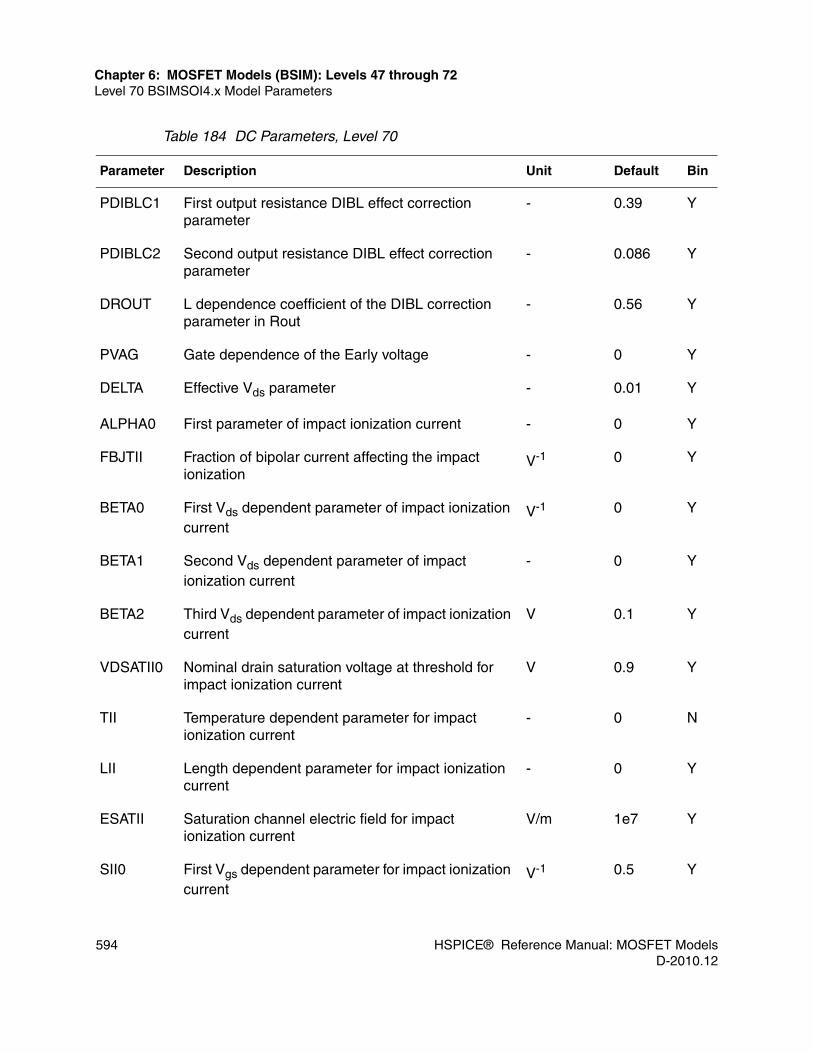
594 HSPICE® Reference Manual: MOSFET ModelsD-2010.12
Chapter 6: MOSFET Models (BSIM): Levels 47 through 72Level 70 BSIMSOI4.x Model Parameters
PDIBLC1 First output resistance DIBL effect correction parameter
- 0.39 Y
PDIBLC2 Second output resistance DIBL effect correction parameter
- 0.086 Y
DROUT L dependence coefficient of the DIBL correction parameter in Rout
- 0.56 Y
PVAG Gate dependence of the Early voltage - 0 Y
DELTA Effective Vds parameter - 0.01 Y
ALPHA0 First parameter of impact ionization current - 0 Y
FBJTII Fraction of bipolar current affecting the impact ionization
V-1 0 Y
BETA0 First Vds dependent parameter of impact ionization current
V-1 0 Y
BETA1 Second Vds dependent parameter of impact ionization current
- 0 Y
BETA2 Third Vds dependent parameter of impact ionization current
V 0.1 Y
VDSATII0 Nominal drain saturation voltage at threshold for impact ionization current
V 0.9 Y
TII Temperature dependent parameter for impact ionization current
- 0 N
LII Length dependent parameter for impact ionization current
- 0 Y
ESATII Saturation channel electric field for impact ionization current
V/m 1e7 Y
SII0 First Vgs dependent parameter for impact ionization current
V-1 0.5 Y
Table 184 DC Parameters, Level 70
Parameter Description Unit Default Bin

HSPICE® Reference Manual: MOSFET Models 595D-2010.12
Chapter 6: MOSFET Models (BSIM): Levels 47 through 72Level 70 BSIMSOI4.x Model Parameters
SII1 Second Vgs dependent parameter for impact ionization current
V-1 0.1 Y
SII2 Third Vgs dependent parameter for impact ionization current
- 0 Y
SIID Vds dependent parameter of drain saturation voltage for impact ionization current
V-1 0 Y
AGIDL Pre-exponent GIDL constant Ω-1 0 Y
BGIDL GIDL exponential coefficient V/m 2.3e9 Y
GDIDL Body-bas effect on GIDL parameter V-3 0.5 Y
EGIDL (NGIDL)
Fitting parameter for band bending for GIDL V 1.2 Y
NTUN Reverse tunneling non-ideality factor for source - 10 Y
NTUND Reverse tunneling non-ideality factor for drain - NTUN Y
NDIODE Diode non-ideality factor for source - 1 Y
NRECF0 Recombination non-ideality factor at forward bias for source
- 2 Y
NRECF0D Recombination non-ideality factor at forward bias for drain
- NRECF0 Y
NRECR0 Recombination non-ideality factor at reverse bias for source
- 10 Y
NRECR0D Recombination non-ideality factor at reverse bias for drain
- NRECR0 Y
ISBJT BJT injection saturation current A/m2 1e-6 Y
IDBJT BJT injection saturation current A/m2 ISBJT Y
Table 184 DC Parameters, Level 70
Parameter Description Unit Default Bin

596 HSPICE® Reference Manual: MOSFET ModelsD-2010.12
Chapter 6: MOSFET Models (BSIM): Levels 47 through 72Level 70 BSIMSOI4.x Model Parameters
ISDIF Body to source/drain injection saturation current A/m2 0 Y
IDDIF Body to source/drain injection saturation current A/m2 ISDIF Y
ISREC Recombination in the depletion saturation current A/m2 1e-5 Y
IDREC Recombination in the depletion saturation current A/m2 ISREC Y
ISTUN Reverse tunneling saturation current A/m2 0 Y
IDTUN Reverse tunneling saturation current A/m2 ISTUN Y
LN Electron/hole diffusion length m 2e-6 N
VREC0 Voltage-dependent parameter for recombination current for source
V 0 Y
VREC0D Voltage-dependent parameter for recombination current for drain
V VREC0 Y
VTUN0 Voltage-dependent parameter for tunneling current for source
V 0 Y
VTUN0D Voltage-dependent parameter for tunneling current for drain
V VTUN0 Y
NBJT Power coefficient of channel length dependency for bipolar current
- 1 Y
LBJT0 Reference channel length for bipolar current m 0.2e-6 Y
VABJT Early voltage for bipolar current V 10 Y
AELY Channel-length dependency of early voltage for bipolar current
V/m 0 Y
AHLI High-level injection parameter for bipolar current for source
- 0 Y
Table 184 DC Parameters, Level 70
Parameter Description Unit Default Bin

HSPICE® Reference Manual: MOSFET Models 597D-2010.12
Chapter 6: MOSFET Models (BSIM): Levels 47 through 72Level 70 BSIMSOI4.x Model Parameters
AHLID High-level injection parameter for bipolar current for drain
- AHLI Y
RBODY Intrinsic body contact sheet resistance Ω/square 0 N
RBSH Extrinsic body contact sheet resistance Ω/square 0 N
RSH Source drain sheet resistance in ohm per square Ω/square 0 N
RHALO Body halo sheet resistance Ω/m 1e15 N
RSW Zero bias lightly-doped source resistance per unit width for RDSMOD=1
Ω-umWR 50 Y
RDW Zero bias lightly-doped drain resistance per unit width for RDSMOD=1
Ω-umWR 50 Y
RSWMIN Lightly-doped source resistance per unit width at Vgs and zero Vbs for RDSMOD=1
Ω-umWR 0 N
RDWMIN Lightly-doped drain resistance per unit width at Vgs and zero Vbs for RDSMOD=1
Ω-umWR 0 N
FRBODY Layout-dependent RBODY multiplier - 1 N
DVTP0 First parameter for Vth shift due to pocket m 0 Y
DVTP1 Second parameter for Vth shift due to pocket V-1 0 Y
PDITS Coefficient for drain-induced Vth shifts V-1 1e-20 Y
PDITSL Length dependence of drain-induced Vth shifts m-1 0 N
PDITSD Vds dependence of drain-induced Vth shifts V-1 0 Y
FPROUT Effect of pocket implant on ROUT degradation V/m0.5 0 Y
MINV VGSTeff fitting parameter for moderate inversion - 0 Y
Table 184 DC Parameters, Level 70
Parameter Description Unit Default Bin

598 HSPICE® Reference Manual: MOSFET ModelsD-2010.12
Chapter 6: MOSFET Models (BSIM): Levels 47 through 72Level 70 BSIMSOI4.x Model Parameters
Table 185 Gate-to-body Tunneling Parameters, Level 70
Parameter Description Unit Default Bin
IGBMOD(IGMOD)
Gate to body tunneling current model selector - 0 N
TOXQM Oxide thickness for IGB calculation m TOX N
NTOX Power term of gate current - 1 N
TOXREF Target oxide thickness m 2.5e-9 N
EBG Effective bandgap in gate current calculation V 1.2 N
ALPHAGB1 First VOX dependent parameter for gate current in inversion V-1 3.5 Y
BETAGB1 Second VOX dependent parameter for gate current in inversion
V-2 0.03 Y
VGB1 Third VOX dependent parameter for gate current in inversion V 300 N
VEVB VAUX parameter for valence band electron tunneling - 0.075 N
ALPHAGB2 First VOX dependent parameter for gate current in accumulation
V-1 0.43 Y
BETAGB1 Second VOX dependent parameter for gate current in accumulation
V-2 0.05 Y
VGB2 Third VOX dependent parameter for gate current in accumulation
V 17 N
VECB VAUX parameter for conduction band electron tunneling - 0.026 N
Table 186 AC and Capacitance Parameters, Level 70
Parameter Description Unit Default Bin
XPART Charge partitioning rate flag - 0 N
CGSO Non-LDD region source-gate overlap capacitance per channel length
F/m calculate N

HSPICE® Reference Manual: MOSFET Models 599D-2010.12
Chapter 6: MOSFET Models (BSIM): Levels 47 through 72Level 70 BSIMSOI4.x Model Parameters
CGDO Non-LDD region drain-gate overlap capacitance per channel length
F/m calculate N
CGEO Gate substrate overlap capacitance per unit channel length
F/m 0 N
CJSWG Source/Drain (gate side) sidewall junction
Capacitance per unit width (normalized to 100nm Tsi)
F/m2 1e-10 N
CJSWGD Drain (gate side) sidewall junction capacitance per unit width (normalized to 100 nm Tsi)
F/m2 CJSWG N
PBSWG Source (gate side) sidewall junction capacitance built-in potential
V 0.7 N
PBSWGD Drain (gate side) sidewall junction capacitance built-in potential
V PBSWG N
MJSWG Source (gate side) sidewall junction capacitance grading coefficient
V 0.5 N
MJSWGD Drain (gate side) sidewall junction capacitance grading coefficient
V MJSWG N
TT Diffusion capacitance transit time coefficient s 1e-12 N
NDIF Power coefficient of channel length dependency for diffusion capacitance
- -1 Y
LDIF0 Channel length dependency coefficient of diffusion capacitance
- 1 N
VSDFB Source/drain bottom diffusion capacitance flatband voltage
V calculate Y
VSDTH Source/drain bottom diffusion capacitance threshold voltage
V calculate Y
CSDMIN Source/drain bottom diffusion minimum capacitance V calculate N
Table 186 AC and Capacitance Parameters, Level 70
Parameter Description Unit Default Bin

600 HSPICE® Reference Manual: MOSFET ModelsD-2010.12
Chapter 6: MOSFET Models (BSIM): Levels 47 through 72Level 70 BSIMSOI4.x Model Parameters
ASD Source/drain bottom diffusion smoothing parameter f - 0.3 N
CSDESW Source/drain sidewall fringing capacitance per unit length
F/m 0 N
CGSL Lightly-doped source-gate region overlap capacitance
F/m 0 Y
CGDL Lightly-doped drain-gate region overlap capacitance F/m 0 Y
CKAPPA Coefficient lightly-doped region overlap capacitance fringing field capacitance
F/m 0.6 Y
CF Gate-to-source/drain fringing field capacitance F/m calculate N
CLC Constant term for the short-channel mode m 0.1e-7 N
CLE Exponential term for the short-channel mode - 0 N
DLC Length offset fitting parameter from C-V m LINT N
DLCB Length offset fitting parameter for body charge m 0 N
DLBG Length offset fitting parameter for backgate charge m 0 N
DWC Width offset fitting parameter from C-V m WINT N
DELVT Threshold voltage adjust for C-V V 0 Y
FBODY Scaling factor for body charge 0 1 N
ACDE Exponential coefficient for charge thickness in CAPMOD=3 for accumulation and depletion regions
m/V 1 Y
MOIN Coefficient for the gate-bias dependent surface potential
V-1/2 5 Y
Table 186 AC and Capacitance Parameters, Level 70
Parameter Description Unit Default Bin

HSPICE® Reference Manual: MOSFET Models 601D-2010.12
Chapter 6: MOSFET Models (BSIM): Levels 47 through 72Level 70 BSIMSOI4.x Model Parameters
Table 187 Temperature Parameters, Level 70
Parameter Description Unit Default Bin
TNOM Temperature at which simulation expects parameters
oC 27 N
UTE Mobility temperature exponent - -1.5 Y
KT1 Temperature coefficient for the threshold voltage
V -0.11 Y
KT1L Channel length dependence of the temperature coefficient for the threshold voltage
V*m 0 Y
KT2 Body-bias coefficient of the Vth temperature effect
- 0.022 Y
UA1 Temperature coefficient for Ua m/V 4.31e-9 Y
UB1 Temperature coefficient for Ub (m/V)2 -7.61e-18 Y
UC1 Temperature coefficient for Uc V-1 -0.056 Y
AT Temperature coefficient for the saturation velocity
m/sec 3.3e4 Y
TCJSWG Temperature coefficient of CJSWGS K-1 0 N
TCJSWGD Temperature coefficient of CJSWGD K-1 TCJSWG N
TPBSWG Temperature coefficient of PBSWGS V/K 0 N
TPBSWGD Temperature coefficient of PBSWGD V/K TPBSWG N
CTH0 Normalized thermal capacity (W-sec)/mC 1e5 N
RTH0 Normalized thermal resistance mC/W 0 N
PRT Temperature coefficient for RDSW Ω-μm 0 Y
NTRECF Temperature coefficient for NRECF - 0 Y

602 HSPICE® Reference Manual: MOSFET ModelsD-2010.12
Chapter 6: MOSFET Models (BSIM): Levels 47 through 72Level 70 BSIMSOI4.x Model Parameters
NTRECR Temperature coefficient for NRECR - 0 Y
XBJT Power dependence of JBJT on the temperature
- 1 Y
XDIF Power dependence of JDIF on the temperature - XBJT Y
XDIFD Power dependence of JDIFD on temperature - XDIF Y
XREC Power dependence of JREC on the temperature
- 1 Y
XRECD Power dependence of JRECD on temperature - XREC Y
XTUN Power dependence of JTUN on the temperature
- 0 Y
ZTUND Power dependence of JRECD on temperature - XTUN Y
WTH0 Minimum width for thermal resistance calculation
m 0 N
SOIMOD SOI model selector■ SOIMOD=0: BSIMPD■ SOIMOD=1: unified model for PD&FD■ SOIMOD=2: ideal FD■ SOIMOD=3: auto selection by BSIMSOI
- 0 N
VBSA Offset voltage due to non-idealities V 0 N
NOFFFD Smoothing parameter in FD module - 1 N
VOFFFD Smoothing parameter in FD module V 0 N
K1B First backgate body effect parameter - 1 N
K2B Second backgate body effect parameter for short channel effect
- 0 N
DK2B Third backgate body effect parameter for short channel effect
- 0 N
Table 187 Temperature Parameters, Level 70
Parameter Description Unit Default Bin

HSPICE® Reference Manual: MOSFET Models 603D-2010.12
Chapter 6: MOSFET Models (BSIM): Levels 47 through 72Level 70 BSIMSOI4.x Model Parameters
DVBD0 First short channel effect parameter in FD module
- 0 N
DVBD1 Second short channel effect parameter in FD module
- 0 N
MOINFD Gain bias dependence coefficient of surface potential in FD module
- 1e3 N
VBS0PD Upper bound of built-in potential lowering for BSIMPD operation
V 0 N
VBS0FD Upper bound of built-in potential lowering for ideal FD operation
V 0.5 N
Table 188 Built-in Potential Lowering Model Parameters, Level 70
Parameter Description Unit Default Bin
SOIMOD SOI model selector■ SOIMOD=0: BSIMPD■ SOIMOD=1: unified model for PD&FD■ SOIMOD=2: ideal FD■ SOIMOD=3: auto selection by BSIMSOI
- 0 N
VBSA Offset voltage due to non-idealities V 0 N
NOFFFD Smoothing parameter in FD module - 1 N
VOFFFD Smoothing parameter in FD module V 0 N
K1B First backgate body effect parameter - 1 N
K2B Second backgate body effect parameter for short channel effect
- 0 N
DK2B Third backgate body effect parameter for short channel effect
- 0 N
Table 187 Temperature Parameters, Level 70
Parameter Description Unit Default Bin

604 HSPICE® Reference Manual: MOSFET ModelsD-2010.12
Chapter 6: MOSFET Models (BSIM): Levels 47 through 72Level 70 BSIMSOI4.x Model Parameters
DVBD0 First short channel effect parameter in FD module
- 0 N
DVBD1 Second short channel effect parameter in FD module
- 0 N
MOINFD Gain bias dependence coefficient of surface potential in FD module
- 1e3 N
VBS0PD Upper bound of built-in potential lowering for BSIMPD operation
V 0 N
VBS0FD Upper bound of built-in potential lowering for ideal FD operation
V 0.5 N
Table 189 Gate Resistance Parameters, Level 70
Parameter Description Unit Default Bin
RGATEMOD Gate resistance model selector■ 0: No gate resistance■ 1: Constant gate resistance■ 2: Rii model with variable resistance■ 3: Rii model with two nodes
- 0 N
RSHG Gate electrode sheet resistance 0.1 Ω/square N
XRCRG1 Parameter for distributed channel resistance effect for intrinsic input resistance
12 - Y
XRCRG2 Parameter to account for the excess channel diffusion resistance for intrinsic input resistance
1 - Y
NGCON Number of gate contacts 1 - N
XGW Distance from the gate contact to the channel edge 0 m N
XGL Offset of the gate length due to variations in patterning 0 m N
Table 188 Built-in Potential Lowering Model Parameters, Level 70
Parameter Description Unit Default Bin

HSPICE® Reference Manual: MOSFET Models 605D-2010.12
Chapter 6: MOSFET Models (BSIM): Levels 47 through 72Level 70 BSIMSOI4.x Model Parameters
Table 190 Body Resistance Parameters, Level 70
Parameter Description Unit Default Bin
RBODYMOD Body resistance model selector■ 0: No body resistance model■ 1: Two-resistor body resistance model
- 0 N
GBMIN Conductance parallel with RBSB/RBDB Ohm 1e-12 N
RBDB Resistance between dbNode and bNode Ohm 50 N
RBSB Resistance between sbNode and bNode Ohm 50 N
Table 191 Noise Parameters, Level 70
Parameter Description Unit Default Bin
FNOIMOD Flicker noise model selector - 1 N
TNOIMOD Thermal noise model selector - 0 N
NTNOI Noise factor for short-channel devices for TNOIMOD=0 or 2
- 1 N
TNOIA Coefficient of channel length dependence of total channel thermal noise
- 1.5 N
TONIB Channel length dependence parameter for channel thermal noise partitioning
- 3.5 N
RNOIA Thermal noise parameter - 0.577 N
RNOIB Thermal noise parameter - 0.37 N
BF Flicker noise length dependence exponent - 2 N
W0FLK Flicker noise width dependence parameter - -1 N

606 HSPICE® Reference Manual: MOSFET ModelsD-2010.12
Chapter 6: MOSFET Models (BSIM): Levels 47 through 72Level 70 BSIMSOI4.x Model Parameters
The parameters in Table 193 improve the BSIM4SOI model to address parasitic BJT-induced avalanche impact ionization current. Contact Synopsys for details.
Table 192 Stress Model Parameters, Level 70
Parameter Description Unit Default Bin
SAREF Reference distance between OD and edge to poly of one side m 1e-6 N
SBREF Reference distance between OD and edge to poly of another side
m 1e-6 N
WLOD Width parameter for stress effect m 0 N
KU0 Mobility degradation/enhancement m 0 Y
KVSAT Saturation velocity degradation/enhancement parameter for stress effect
m 0 N
KVTH0 Threshold shift parameter for stress effect V-m 0 Y
TKU0 Temperature coefficient of KU0 - 0 N
LLODKU0 Length parameter for KU0 stress effect - 0 N
WLODKU0 Width parameter for KU0 stress effect - 0 N
LLODVTH Length parameter for Vth stress effect - 0 N
WLODVTH Width parameter for Vth stress effect - 0 N
STK2 K2 shift factor related to Vth0 change m 0 N
LODK2 K2 shift modification factor for stress effect - 1 N
STETA0 Eta0 shift factor related to Vth0 change m 0 N
LODETA0 Eta0 shift modification factor for stress effect - 1 N
Table 193 Avalanche Impact Ionization Parameters, Level 70
Parameter Description Unit Default Notes
IIMOD Impact ionization model selector - 0 (original II model)
=1 selects the new II model

HSPICE® Reference Manual: MOSFET Models 607D-2010.12
Chapter 6: MOSFET Models (BSIM): Levels 47 through 72Level 70 BSIMSOI4.x Model Parameters
Parameter Range Limit for BSIM4SOI4 Level 70Simulation reports either a warning or a fatal error if BSIMSOI4 parameters fall outside predefined ranges. These range limitations prevent (or at least warn of) potential numerical problems.
To control the maximum number of simulation warning messages printing to the output file, use:
.OPTION WARNLIMIT=#
In the preceding .OPTION statement, # is the maximum number of warning messages that simulation reports. The default WARNLIMIT value is 1. In some cases (as noted in Table 194 below), simulation checks parameters only if you set the PARMAMCHK=1 model parameter.
EBJTII Impact ionization parameter for BJT part 1/V 0.0 -
CBJTII Length scaling parameter for II BJT part m/V 0.0 -
VBCI Internal B-C built-in potential V 0.7 -
ABJTII Exponent factor for avalanche current - 0.0 -
MBJTII Internal B-C grading coefficient - 0.4 -
TVBCI Temperature coefficient for VBCI - 0.0 -
Table 194 Model Parameter Range Limit, Level 70
Parameter Limit
wlod < 0 warn
kvsat < -1.0, >1.0 warn
Lpe0 < -leff fatal
saref <= 0 fatal
Table 193 Avalanche Impact Ionization Parameters, Level 70
Parameter Description Unit Default Notes
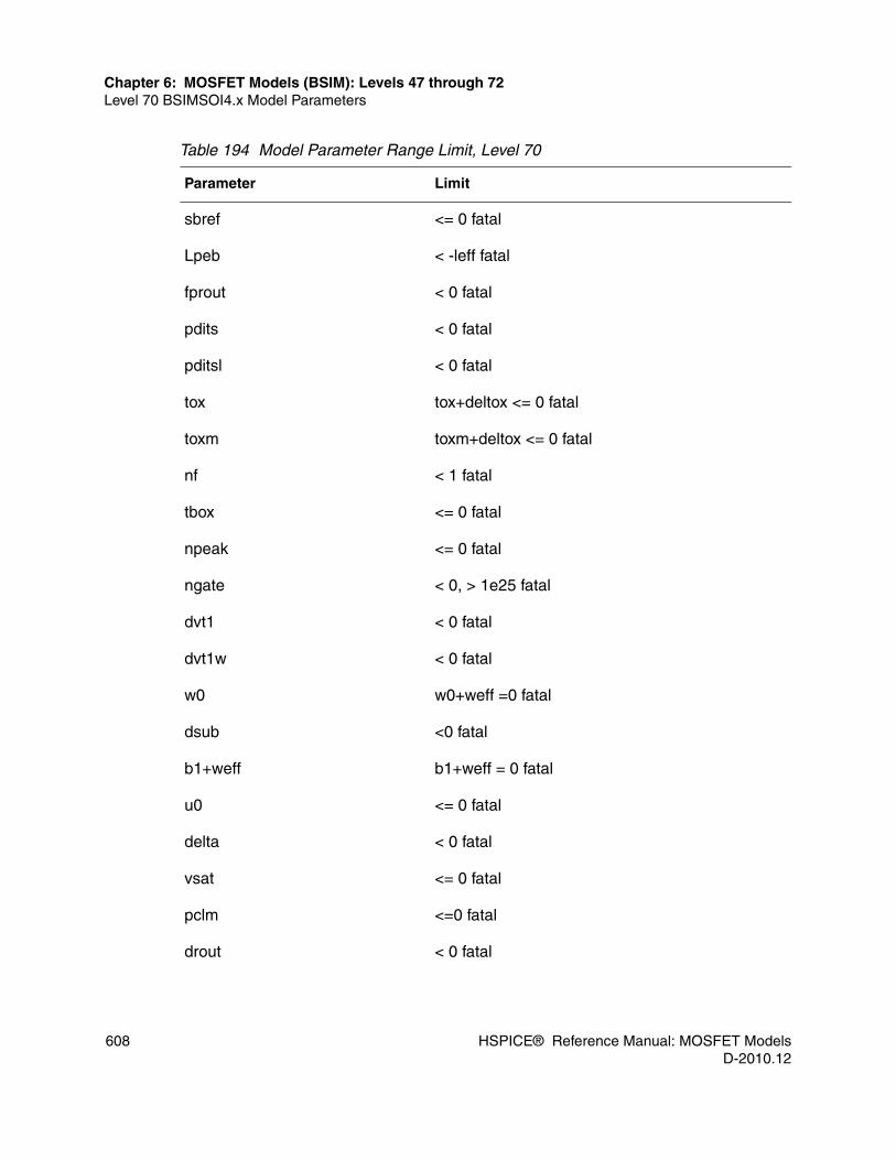
608 HSPICE® Reference Manual: MOSFET ModelsD-2010.12
Chapter 6: MOSFET Models (BSIM): Levels 47 through 72Level 70 BSIMSOI4.x Model Parameters
sbref <= 0 fatal
Lpeb < -leff fatal
fprout < 0 fatal
pdits < 0 fatal
pditsl < 0 fatal
tox tox+deltox <= 0 fatal
toxm toxm+deltox <= 0 fatal
nf < 1 fatal
tbox <= 0 fatal
npeak <= 0 fatal
ngate < 0, > 1e25 fatal
dvt1 < 0 fatal
dvt1w < 0 fatal
w0 w0+weff =0 fatal
dsub <0 fatal
b1+weff b1+weff = 0 fatal
u0 <= 0 fatal
delta < 0 fatal
vsat <= 0 fatal
pclm <=0 fatal
drout < 0 fatal
Table 194 Model Parameter Range Limit, Level 70
Parameter Limit

HSPICE® Reference Manual: MOSFET Models 609D-2010.12
Chapter 6: MOSFET Models (BSIM): Levels 47 through 72Level 70 BSIMSOI4.x Model Parameters
pd < w warn
ps < w warn
clc < 0 fatal
noff < 0.1, > 4.0 warn
lodk2 <= 0 warn
lodeta0 <= 0 warn
moin < 5, > 25 warn
moinfd < 5 warn
acde < 0.1, > 1.6 warn
if paramchk=1 following parameter limit range is added
leff <= 5e-8 warn
leffcv <= 5e-8 warn
weff <= 1e-7 warn
weffcv <= 1e-7 warn
lpe0 < 0 warn
npeak <= 1e15, >= 1e21 warn
nsub <= -1e21, >= 1e21 warn
ngate < 1e18 warn
dvt0 < 0 warn
w0 w0+weff < 1e-7 warn
nfactor < 0 warn
Table 194 Model Parameter Range Limit, Level 70
Parameter Limit

610 HSPICE® Reference Manual: MOSFET ModelsD-2010.12
Chapter 6: MOSFET Models (BSIM): Levels 47 through 72Level 70 BSIMSOI4.x Model Parameters
cdsc < 0 warn
cdscd < 0 warn
eta0 < 0 warn
b1 b1+weff < 1e-7 warn
a2 < 0.01, > 1 warn
rdsw < warn
rds0 < 0.001 warn
vsattemp < 1e3 warn
pdibl1 < 0 warn
pdibl2 < 0 warn
cgdo < 0 warn
cgso < 0 warn
cgeo < 0 warn
ntun < 0 warn
ntund < 0 warn
ndiode < 0 warn
ndioded < 0 warn
isbjt < 0 warn
idbjt < 0 warn
isdiff < 0 warn
iddiff < 0 warn
Table 194 Model Parameter Range Limit, Level 70
Parameter Limit

HSPICE® Reference Manual: MOSFET Models 611D-2010.12
Chapter 6: MOSFET Models (BSIM): Levels 47 through 72Level 70 BSIMSOI4.x Model Parameters
isrec < 0 warn
idrec < 0 warn
istun < 0 warn
idtun < 0 warn
tt < 0 warn
csdmin < 0 warn
csdesw < 0 warn
asd < 0 warn
rth0 < 0 warn
cth0 < 0 warn
rbody < 0 warn
rbsh < 0 warn
nigc <= 0 warn
poxedge <= 0 warn
pigcd <= 0 warn
wth0 < 0 warn
rhalo < 0 warn
ntox < 0 warn
toxref < 0 warn
ebg < 0 warn
vevb < 0 warn
Table 194 Model Parameter Range Limit, Level 70
Parameter Limit

612 HSPICE® Reference Manual: MOSFET ModelsD-2010.12
Chapter 6: MOSFET Models (BSIM): Levels 47 through 72Level 70 BSIMSOI4.x Model Parameters
alphagb1 < 0 warn
betagb1 < 0 warn
vgb1 < 0 warn
vecb < 0 warn
alphagb2 < 0 warn
betagb2 < 0 warn
vgb2 < warn
toxqm < 0 warn
voxh < 0 warn
beltavox <= 0 warn
k1w1 < 0 warn
k1w2 < 0 warn
ketas < 0 warn
dwbc < 0 warn
beta0 < 0 warn
beta1 < 0 warn
beta2 < 0 warn
tii < 0 warn
lii < 0 warn
sii1 < 0 warn
sii2 < 0 warn
Table 194 Model Parameter Range Limit, Level 70
Parameter Limit

HSPICE® Reference Manual: MOSFET Models 613D-2010.12
Chapter 6: MOSFET Models (BSIM): Levels 47 through 72Level 70 BSIMSOI4.x Model Parameters
siid < 0 warn
fbjtii < 0 warn
vrec0 < 0 warn
vrec0d < 0 warn
vtun0 < 0 warn
vtun0d < 0 warn
nbjt < 0 warn
aely < 0 warn
ahli < 0 warn
ahlid < 0 warn
rbody < 0 warn
rbsh < 0 warn
ntrecf < 0 warn
ntrecr < 0 warn
tcjswg < 0 warn
tpbswg < 0 warn
tcjswgd < 0 warn
tpbswgd < 0 warn
acde < 0.1, > 1.6 warn
moin < 5, > 25 warn
dlbg < 0 warn
Table 194 Model Parameter Range Limit, Level 70
Parameter Limit

614 HSPICE® Reference Manual: MOSFET ModelsD-2010.12
Chapter 6: MOSFET Models (BSIM): Levels 47 through 72Level 71 TFT Model
Level 71 TFT Model
Thin-film transistor (TFT) process technology has been the industry mainstream technology of choice to implement various flat-panel display applications. While there exist many similarities in the electrical terminal characteristics between TFTs and their crystalline silicon counterparts, unique charge trapping/de-trapping and charge carrier transport mechanisms associated with the grains and grain boundaries in the channel region have led to significant technical challenges in TFT device modeling for accurate and scalable SPICE simulations.
The Level 71 TFT model is a unified model. It is used for polycrystalline silicon (p-si), but it is also applicable to amorphous silicon (a-si). The model has been developed based on BSIMSOI, with high accuracy in geometrical, bias, and temperature scaling. It explicitly and accurately considers the following physical effects: non-ideality of the subthreshold swing, quasi-saturation, bias-dependent source/drain resistance, kink in the saturation region, self heating, large leakage current, and many other related device behaviors.
This HSPICE TFT model is fully supported by Synopsys' parameter extraction tool, Aurora. For detail on usage, contact the Synopsys support teams.
The following sections discuss these topics:
agidl < 0 warn
bgidl < 0 warn
cgidl < 0 warn
egidl < 0 warn
esatii <= 0 warn
xj > tsi warn
capmod < 2 warn
Table 194 Model Parameter Range Limit, Level 70
Parameter Limit

HSPICE® Reference Manual: MOSFET Models 615D-2010.12
Chapter 6: MOSFET Models (BSIM): Levels 47 through 72Level 71 TFT Model
■ General Syntax for the Level 71 Model
General Syntax for the Level 71 ModelThe general syntax for including a LEVEL 71 model element in a netlist is:
Mxxx nd ng ns ne [np] [nb] [nT] mname [L=val]+ [M=val] [AS=val] [PS=val] [NRD=val]+ [NRS=val] [NRB=val] [CTH0=val]+ [NSEG=val] [PDBCP=val] [PSBCP=val] [AGBCP=val]+ [AEBCP=val] [DELTOX=val] [TNODEOUT]+ [off] [FRBODY] [BJToff=val] [IC=Vds, Vgs, Vbs, Ves, Vps]
Argument Descriptions
Table 195 TFT Model Arguments and Options
Argument Description
Mxxx TFT element name. Must begin with M, followed by up to 1023 alphanumeric characters.
nd Drain terminal node name or number.
ng Front gate node name or number.
ns Source terminal node name or number.
ne Back gate (or substrate) node name or number.
np External body contact node name or number.
nb Internal body node name or number.
nT Temperature node name or number.
mname MOSFET model name reference.
L TFT channel length in meters. This parameter overrides DEFL in an OPTIONS statement. Default=DEFL with a maximum of 0.1m.

616 HSPICE® Reference Manual: MOSFET ModelsD-2010.12
Chapter 6: MOSFET Models (BSIM): Levels 47 through 72Level 71 TFT Model
W MOSFET channel width in meters. This parameter overrides DEFW in an OPTIONS statement. Default=DEFW.
M Multiplier to simulate multiple TFT in parallel. The M setting affects all channel widths, diode leakages, capacitances, and resistances. Default=1.
AD Drain diffusion area. Overrides .OPTION DEFAD statement. Default=DEFAD.
AS Source diffusion area. Overrides .OPTION DEFAS statement. Default=DEFAS.
PD Drain junction perimeter, including channel edge. Overrides .OPTION DEFPD.
PS Source junction perimeter including channel edge. Overrides .OPTION DEFPS.
NRD Number of squares of drain diffusion for the drain series resistance. Overrides .OPTION DEFNRD.
NRS Number of squares of source diffusion for the source series resistance. Overrides .OPTION DEFNRS.
NRB Number of squares for the body series resistance.
FRBODY Coefficient of the distributed body resistance effects. Default=1.0
RTH0 Thermal resistance per unit width:
If you do not specify RTH0, simulation extracts it from the model card.
If you specify RTH0, it overrides RTH0 in the model card.
CTH0 Thermal capacitance per unit width:
If you do not specify CTH0, simulation extracts it from the model card.
If you specify CTH0, it overrides CTH0 in the model card.
NBC Number of body contact isolation edge.
NSEG Number of segments for partitioning the channel width.
PDBCP Parasitic perimeter length for the body contact a the drain side.
Table 195 TFT Model Arguments and Options (Continued)
Argument Description

HSPICE® Reference Manual: MOSFET Models 617D-2010.12
Chapter 6: MOSFET Models (BSIM): Levels 47 through 72Level 71 TFT Model
Level 71 Model ParametersThe following tables describe the Level 71 Model Control, Process, DC, AC and Capacitance, Temperature, and A.4 Bias Control for Source Model parameters.
PSBCP Parasitic perimeter length for the body contact at the source side.
AGBCP Parasitic gate-to-body overlap area for the body contact.
AEBCP Parasitic body-to-substrate overlap area for the body contact.
VBSUSR Optional initial Compared value of Vbs that you specify for transient analysis.
DELTOX Shift in gate oxide thickness (TOX). That is, the difference between the electrical and physical gate oxide/insulator thicknesses.
TNODEOUT Temperature node flag indicating the use of the T node.1 See footnote below.
OFF Sets the initial condition of the element to OFF in DC analysis.
BJTOFF Turning off BJT if equal to 1.
IC Initial guess in the order (drain, front gate, internal body, back gate, external voltage). (ignores Vps for 4-terminal devices) Use these only if you specify UIC in the .TRAN statement. The .IC statement overrides it.
1. If you do not set TNODEOUT, you can specify 3 nodes for a device to float the body. Specifying 4 nodes implies that the 4th node is the external body contact node with a body resistance between the internal and external terminals. This configuration applies to a distributed body resistance simulation.If you set TNODEOUT, simulation interprets the last node as the temperature node. You can specify 4 nodes to float the device. Specifying 5 nodes implies body contact. 6 nodes is a body-contacted case with an accessible internal body node. You can use the temperature node to simulate thermal coupling.
Table 196 Model Control Parameters
Parameter Unit Default Description
MOBMOD - 1 Mobility model selector
Noimod - 1 Flag for the noise model
Table 195 TFT Model Arguments and Options (Continued)
Argument Description

618 HSPICE® Reference Manual: MOSFET ModelsD-2010.12
Chapter 6: MOSFET Models (BSIM): Levels 47 through 72Level 71 TFT Model
SHMOD - 0 Flag for self-heating:
0=no self-heating
1=self-heating
TFTMOD - 0 Flag for the transistor operation mode:
0=partially depleted
1=dynamic depleted
2=partially depleted
Table 197 Process Parameters
Parameter Unit Default Description
Parameter Unit Default Description
DTOXCV Difference between the electrical and physical gate oxide thicknesses, due to the effects of the gate poly depletion and the finite channel charge layer thickness.
Nch 1/cm3 1e15 Channel doping concentration
Ngate 1/cm3 0 Poly gate doping concentration
Nsub 1/cm3 6.0e16 Substrate doping concentration
Tox m 4.5e-8 Gate oxide thickness
Tsi m 1.0e-8 Silicon film thickness
Table 198 DC Parameters
Parameter Unit Default Description
a0 - 2.5 Bulk charge effect coefficient for the channel length
Table 196 Model Control Parameters (Continued)
Parameter Unit Default Description

HSPICE® Reference Manual: MOSFET Models 619D-2010.12
Chapter 6: MOSFET Models (BSIM): Levels 47 through 72Level 71 TFT Model
a1 1/V 0.68 First non-saturation effect parameter
a2 - 0.18 Second non-saturation effect parameter
aely V/m -0.1 Channel length dependency of the early voltage for the bipolar current
agidl 1/W 1e-7 GIDL constant
ags 1/V 0.15 Gate bias coefficient of Abulk
ahli - 0.1 High-level injection parameter for the bipolar current
alpha0 m/V 1e-12 First parameter of the impact ionization current
b0 m 4.5e-8 Bulk charge effect coefficient for the channel width
b1 m 1e-7 Bulk charge effect width offset
beta0 1/V 40 First Vds dependence parameter of the impact ionization current
beta1 - 5 Second Vds dependence parameter of the impact ionization current
beta2 V 0 Third Vds dependence parameter of the impact ionization current
betag - 3 Gate induced grain boundary barrier lowering coefficient
bgidl V/m 9.5e9 GIDL exponential coefficient
cdsc F/m2 -1e-3 Drain/source to the channel coupling capacitance
cdscb F/m2 0 Body-bias sensitivity of cdsc
cdscd F/m2 1e-3 Drain-bias sensitivity of cdsc
cgidl - 3.7e-2 Body voltage factor for gidl
Table 198 DC Parameters (Continued)
Parameter Unit Default Description

620 HSPICE® Reference Manual: MOSFET ModelsD-2010.12
Chapter 6: MOSFET Models (BSIM): Levels 47 through 72Level 71 TFT Model
cit F/m2 0.0 Interface trap capacitance
delta - 2.3 Effective Vds parameter
dgidl - 2.5 Electric field exponent factor for gidl
drout - 0.2 L dependence coefficient of the DIBL correction parameter in Rout
dsub - 5 DIBL coefficient exponent
dvt0 - 0 First coefficient of the short-channel effect on Vth
dvt0w - 0 First coefficient of the narrow width effect on Vth for a small channel length
dvt1 - 1 Second coefficient of the short-channel effect on Vth
dvt1w - 5.3e6 Second coefficient of the narrow width effect on Vth for a small channel length
dvt2 1/V -0.032 Body-bias coefficient of the short-channel effect on Vth
dvt2w 1/V -0.032 Body-bias coefficient of the narrow width effect on Vth for a small channel length
dwb m/V1/2 0.0 Coefficient of the substrate body bias dependence of Weff
dwbc m 0.0 Width offset for the body contact isolation edge
dwg m/V 2.3e-8 Coefficient of the gate dependence of Weff
esati V/m 1.e7 Saturation channel electric field for the impact ionization current
eta0 - 0 DIBL coefficient in the subthreshold region
etab 1/V -0.07 Body-bias coefficient for the DIBL effect in the subthreshold region
Table 198 DC Parameters (Continued)
Parameter Unit Default Description

HSPICE® Reference Manual: MOSFET Models 621D-2010.12
Chapter 6: MOSFET Models (BSIM): Levels 47 through 72Level 71 TFT Model
fbjtii - 0.0 Fraction of the bipolar current affecting the impact ionization
ggidl - 6e-1 Gate voltage coefficient for gidl
Isbjt A/m2 1.4e-7 BJT injection saturation current
Isdif A/m2 5e-5 Body to source/drain injection saturation current
Isrec A/m2 1.0e-5 Recombination in the depletion saturation current
Istun A/m2 0.0 Reverse tunneling saturation current
k1 V1/2 0.35 First-order body effect coefficient
k1w1 m 0 First-order effect width dependent parameter
k1w2 m 0 Second-order effect width dependent parameter
k2 - -2e-2 Second-order body effect coefficient
k3 - 6e-4 Narrow coefficient
k3b 1/V 0 Body effect coefficient of k3
kb1 - 1 Backgate body charge coefficient
keta 1/V -4.6e-2 Body-bias coefficient of the bulk charge effect
Ketas V 0.0 Surface potential adjustment for the bulk charge effect
kg - 1 Offset voltage for gate induced grain boundary barrier lowering
Lbjt0 m 1.3e-7 Reference channel length for the bipolar current
lii - 2.8e-6 Channel length dependence parameter for the impact ionization current
lint m 0.0 Length offset fitting parameter from I-V without bias
Table 198 DC Parameters (Continued)
Parameter Unit Default Description

622 HSPICE® Reference Manual: MOSFET ModelsD-2010.12
Chapter 6: MOSFET Models (BSIM): Levels 47 through 72Level 71 TFT Model
lgb1 - 1e-2 Grain boundary factor inducing effective channel length decrease
lgb2 - 7e-4 Depletion near grain boundary inducing effective channel length decrease
lgb3 - 2e-2 Gate voltage factor for effective channel length
ln m 1.8-6 Electron/hole diffusion length
nbjt - 1.3 Power coefficient of the channel length dependency for the bipolar current
ndio - 0.5 Diode non-ideality factor
nln - 2 Channel length exponent for amplification coefficient of parasitic BJT
nfactor - 20 Subthreshold swing factor
ngidl V -22 GIDL Vds enhancement coefficient
nlx m 1.5e-6 Lateral non-uniform doping parameter
nrecf0 - 2.0 Recombination non-ideality factor at the forward bias
nrecr0 - 10 Recombination non-ideality factor at the reversed bias
ntun - 10.0 Reverse tunneling non-ideality factor
pclm - 9e-4 Channel length modulation parameter
PDIBLC1 - 1 Correction parameter for the DIBL effect of the first output resistance
pdiblc2 - 1.5e-3 Correction parameter for the DIBL effect of the second output resistance
prwb 1/V -7.7e-7 0
prwg 1/V1/2 -1e-2 Gate-bias effect coefficient of Rdsw
Table 198 DC Parameters (Continued)
Parameter Unit Default Description

HSPICE® Reference Manual: MOSFET Models 623D-2010.12
Chapter 6: MOSFET Models (BSIM): Levels 47 through 72Level 71 TFT Model
pvag - 5.6e2 Gate dependence of the Early voltage
rbody ohm/m2 0.0 Intrinsic body contact sheet resistance
rbsh ohm/m2 0.0 Extrinsic body contact sheet resistance
rdsw ohm/m2 7e4 Parasitic resistance per unit width
rsh ohm/square 0.0 Source/drain sheet resistance in ohm per square
sii0 1/V 0.37 First Vgs dependence parameter for the impact ionization current
sii1 1/V 0.08 Second Vgs dependence parameter for the impact ionization current
sii2 1/V 0.08 Third Vgs dependence parameter for the impact ionization current
siid 1/V 5e-3 Vds dependence parameter of the drain saturation voltage for the impact ionization current
tii - 0 Temperature dependence parameter for the impact ionization current
u0 cm2/(V-sec) NMOS-600 PMOS-200
Mobility at Temp=Tnom
ua m/V 9.6e-9 First-order mobility degradation coefficient
ub (m/V)2 1e-21 Second-order mobility degradation coefficient
uc 1/V -4e-11 Body-effect of the mobility degradation coefficient
ug m2/(V-sec) 9e-2 Grain boundary barrier scattering mobility at Temp=Tnom
vabjt V 10 Early voltage for the bipolar current
vdsatii0 V 0.6 Nominal drain saturation voltage at threshold for the impact ionization current
Table 198 DC Parameters (Continued)
Parameter Unit Default Description

624 HSPICE® Reference Manual: MOSFET ModelsD-2010.12
Chapter 6: MOSFET Models (BSIM): Levels 47 through 72Level 71 TFT Model
VECB v 0.026v Electron tunneling from the conduction band
VEVB v 0.075v Electron tunneling from the valence band
voff v -0.6 Offset voltage in the subthreshold region for large W and L values
Vrec0 V 0.0 Voltage dependent parameter for the recombination current
vsat m/sec 5e5 Saturation velocity at Temp=Tnom
vth0 v NMOS 0.7 PMOS -0.7
Threshold voltage @ Vbs=0 for a long, wide device
Vtun0 V 0.0 Voltage dependent parameter for the tunneling current
w0 m 2.5e-5 Narrow width parameter
wint m 0.0 Width offset fitting parameter from I-V without bias
wr - 0.8 Width offset from Weff for the Rds calculation
Table 199 AC and Capacitance Parameters
Parameter Unit Default Description
acde m/V 1.0 Exponential coefficient for the charge thickness in the CapMod=3 for the accumulation and depletion regions
asd V 0.3 Smoothing parameter for the source/drain bottom diffusion
cf F/m cal. Fringing field capacitance of the gate-to-source/drain
cgdl F/m 0.0 Overlap capacitance for the lightly-doped drain-gate region
cgdo F/m 0 Non LDD region drain-gate overlap capacitance per channel length
CGEO F/m 0 Gate Substrate overlap capacitance per unit channel length
cgsl F/m 0.0 Overlap capacitance for the lightly-doped source-gate region
Table 198 DC Parameters (Continued)
Parameter Unit Default Description

HSPICE® Reference Manual: MOSFET Models 625D-2010.12
Chapter 6: MOSFET Models (BSIM): Levels 47 through 72Level 71 TFT Model
cgso F/m cal. Calculated Non LDD region source-gate overlap capacitance per channel length
cjswg F/m2 1.e-10 Source/drain (gate side) sidewall junction capacitance per unit width (normalized to 100nm Tsi)
ckappa F/m 0.6 Coefficient for the fringing field capacitance for the overlap capacitance in the lightly-doped region
clc m 0.1e-7 Constant term for the short-channel model
cle - 0.0 Exponential term for the short-channel model
csdesw F/m 0.0 Fringing capacitance per unit length for the source/drain sidewall
csdmin V cal. Minimum capacitance for the source/drain bottom diffusion
delvt V 0.0 Threshold voltage adjustment for C-V
dlbg m 0 Length offset fitting parameter for the backgate charge
dlc m lint Length offset fitting parameter for the gate charge
dlcb m lint Length offset fitting parameter for the body charge
dwc m wint Width offset fitting parameter from C-V
fbody - 1.0 Scaling factor for the body charge
Ldif0 - 1 Channel length dependency coefficient of the diffusion cap.
mjswg V 0.5 Grading coefficient of the source/drain (gate side) sidewall junction capacitance
moin V1/2 15.0 Coefficient for the gate-bias dependent surface potential
Ndif - -1 Power coefficient of the channel length dependency for the diffusion capacitance
pbswg V 0.7 Built-in potential of the source/drain (gate side) sidewall junction capacitance
Table 199 AC and Capacitance Parameters (Continued)
Parameter Unit Default Description
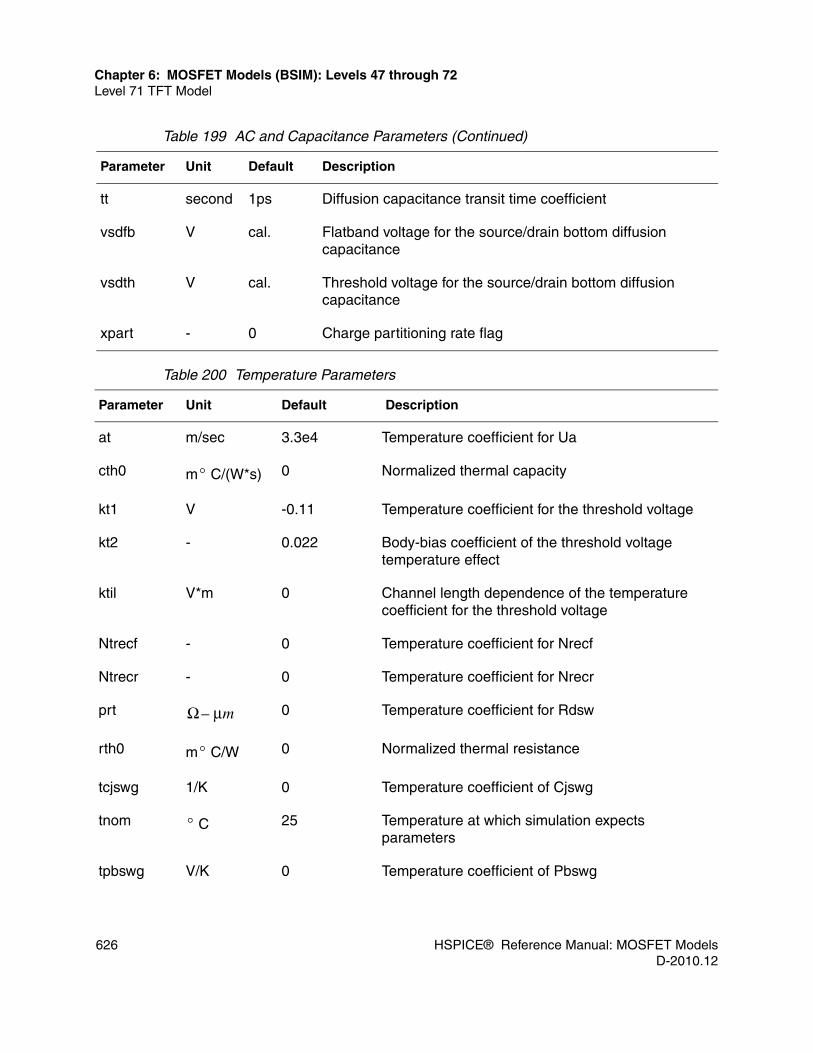
626 HSPICE® Reference Manual: MOSFET ModelsD-2010.12
Chapter 6: MOSFET Models (BSIM): Levels 47 through 72Level 71 TFT Model
tt second 1ps Diffusion capacitance transit time coefficient
vsdfb V cal. Flatband voltage for the source/drain bottom diffusion capacitance
vsdth V cal. Threshold voltage for the source/drain bottom diffusion capacitance
xpart - 0 Charge partitioning rate flag
Table 200 Temperature Parameters
Parameter Unit Default Description
at m/sec 3.3e4 Temperature coefficient for Ua
cth0 m C/(W*s) 0 Normalized thermal capacity
kt1 V -0.11 Temperature coefficient for the threshold voltage
kt2 - 0.022 Body-bias coefficient of the threshold voltage temperature effect
ktil V*m 0 Channel length dependence of the temperature coefficient for the threshold voltage
Ntrecf - 0 Temperature coefficient for Nrecf
Ntrecr - 0 Temperature coefficient for Nrecr
prt 0 Temperature coefficient for Rdsw
rth0 m C/W 0 Normalized thermal resistance
tcjswg 1/K 0 Temperature coefficient of Cjswg
tnom C 25 Temperature at which simulation expects parameters
tpbswg V/K 0 Temperature coefficient of Pbswg
Table 199 AC and Capacitance Parameters (Continued)
Parameter Unit Default Description
°
Ω μm–
°
°

HSPICE® Reference Manual: MOSFET Models 627D-2010.12
Chapter 6: MOSFET Models (BSIM): Levels 47 through 72Level 71 TFT Model
ua1 m/V 4.31e-9 Temperature coefficient for Ua
ub1 (m/V)2 -7.61e-18 Temperature coefficient for Ub
uc1 1/V -0.056 Temperature coefficient for Uc
ute - -1.5 Mobility temperature exponent
xbjt - 1 Power dependence of jbjt on the temperature
xdif - Same as XBJT
Power dependence of jdif on the temperature
xrec - 1 Power dependence of jrec on the temperature
xtun - 0 Power dependence of jtun on the temperature
Table 201 A.4 Parameters for Bias-Dependent Source (Rs)/Drain(Rd) Models
Parameter Unit Default Description
rsw ohm(um)^wr 100.0 Zero bias lightly-doped source resistance Rs(V) per unit width for RSMOD=1
rswmin ohm(um)^wr 0.0 Lightly-doped source resistance per unit width at high Vgs and zero Vbs for RSMOD=1
prwbs V^-0.5 0.0 Body-bias dependence of LDD resistance in source side
prwgs V^-1 1.0 Gate-bias dependence of LDD resistance in source side
prwss V^-1 1.0 External source-bias and gate-bias dependence of LDD resistance in source side
ersg1 - 1.0 Gate-bias dependent parameter in PRWGS
ersg2 - 1.0 Gate-bias dependent parameter in PRWSS
erss - 1.0 External source voltage dependent parameter in PRWSS
Table 200 Temperature Parameters (Continued)
Parameter Unit Default Description

628 HSPICE® Reference Manual: MOSFET ModelsD-2010.12
Chapter 6: MOSFET Models (BSIM): Levels 47 through 72Level 71 TFT Model
crs 1.0 Coefficient of Rs due to gate and external source bias
rdw ohm(um)^wr 100.0 Zero bias lightly-doped drain resistance Rd(V) per unit width for RDMOD=1
rdwmin ohm(um)^wr 0.0 Lightly-doped drain resistance per unit width at high Vgs and zero Vbs for RDMOD=1
prwdb Same as prwbs
Body-bias dependence of LDD resistance in drain side
prwgd Same as prwgs
Gate-bias dependence of LDD resistance in drain side
prwdd Same as prwss
External drain-bias and gate-bias dependence of LDD resistance in drain side
erdg1 Same as ersg1
Gate-bias dependent parameter in PRWGD
erdg2 Same as ersg2
Gate-bias dependent parameter in PRWDD
erdd Same as erss External drain voltage dependent parameter in PRWDD
crd Same as crs Coefficient of Rd due to gate and external drain bias
rswmin0 Ohm 0.0 Source resistance constant component
rdwmin0 Ohm 0.0 Drain resistance constant component
wr - 0.0 Width dependence exponent of lightly-doped source and drain resistance
deltavgs - 1.0e-4 Smoothing parameter for RS dependence on VGS
deltavgd Same as deltavgs
Smoothing parameter for RD dependence on VGD
Table 201 A.4 Parameters for Bias-Dependent Source (Rs)/Drain(Rd) Models
Parameter Unit Default Description

HSPICE® Reference Manual: MOSFET Models 629D-2010.12
Chapter 6: MOSFET Models (BSIM): Levels 47 through 72Level 72 BSIM-CMG MOSFET Model
Level 72 BSIM-CMG MOSFET Model
The BSIM-CMG model (HSPICE Level 72) is a compact model to describe the behavior of multiple-gate MOSFET devices. There are two sub-modules for this HSPICE built-in model:■ 3-terminal SOIMG module for the BSIM-CMG SOI model ■ 4-terminal BULKMG module for the BSIM-CMG BULK model
All important multi-gate transistor behaviors are captured by this model. Volume inversion is included in the solution of Poisson’s equation; hence the subsequent I-V formulation automatically captures the volume inversion effect. Analysis of the electrostatic potential in the body of MG MOSFETs provides the model equation for short channel effects (SCE). The extra electrostatic control from the top gate (tri-gate) or top/bottom gates (omega-gate or all-around-gate) is also captured in the short channel model. The SCE model predicts the threshold (Vt) roll-off, drain-induced-barrier lowering (DIBL) and subthreshold slope degradation in close agreement with 2-D device simulation results.
Included in the model are other important effects such as: mobility degradation, multiple surface-orientations, velocity saturation, velocity overshoot, series resistance, channel length modulation, quantum mechanical effects, poly depletion, gate tunneling current, gate-induced-drain-leakage, and parasitic capacitance models.
See also: Output Templates for BSIMMG (BSIM-CMG) Level 72 on page 45.
The following sections discuss these topics:■ BSIM-CMG 104 Updates■ BSIM-CMG 103 Updates■ General Syntax for BSIM-CMG Model■ Deactivating Equations in BSIM-CMG■ BSIM-CMG Complete Parameter Lists

630 HSPICE® Reference Manual: MOSFET ModelsD-2010.12
Chapter 6: MOSFET Models (BSIM): Levels 47 through 72Level 72 BSIM-CMG MOSFET Model
BSIM-CMG 104 UpdatesBSIM-CMG 104.1The following BSIM-CMG 104.1 updates became available for HSPICE with the HSPICE E-2010.12 release:
1. Asymmetric DIBL parameters supported.
2. Bulk-Charge is made bias independent through correct implementation.
3. CLMMOD=1 case replaced with newer model.
4. Many bug fixes were implemented.
BSIM-CMG 104.0The following BSIM-CMG 104 updates became available for HSPICE with the HSPICE D-2010.03-SP1 release:
1. Channel length modulation model CLMMOD=1 is added based on the BSIM4 formulation.
2. Instance parameters NRS and NRD and associated equations are added based on the BSIM4 formulation.
3. The equations associated with parameter PVAG are modified to provide more flexibility for output conductance fitting.
4. Added a New Impact Ionization Current Model and Model Switch IIMOD; BSIM4 based Iii model into IIMOD=1 block and BSIMSOI based Iii model into IIMOD=2 block.
5. Improved the Gate Electrode Resistance Model; introduced new parameters RGEXT and RGFIN and removed parameter RGELTD.
6. Changed the Internal Resistance formula.
7. Implemented many bug fixes.
BSIM-CMG 103 UpdatesThe following BSIM-CMG 103 updates became available for HSPICE with the HSPICE D-2010.03 release:
1. This release supports a Cylindrical gate geometry through GEOMOD = 3 with an associated short channel scale length and quantum effects model.
2. The existing I-V has been enhanced to model Poly-depletion accurately.

HSPICE® Reference Manual: MOSFET Models 631D-2010.12
Chapter 6: MOSFET Models (BSIM): Levels 47 through 72Level 72 BSIM-CMG MOSFET Model
3. Self-heating is now supported with addition of a Temperature node.
4. Junction Capacitance and Junction Current equations were revamped with source-drain asymmetry supported. The asymmetry is now also in GIDL/GISL currents.
5. Length-dependent equations have been added for a Global Parameter Extraction without binning.
6. SHMOD, RGATEMOD, NQSMOD and RDSMOD also control the number of internal nodes for faster simulations.
7. Many bug fixes were implemented.
General Syntax for BSIM-CMG ModelThe general syntax for including a BSIM-CMG model element in a netlist is:
Mxxx nd ng ns [nb] mname [L=val] [M=val].model mname n(p)mos LEVEL=72 VERSION=val …
Level 72 is the BSIM-CMG model in HSPICE. Before BSIMCMG102, the model parameter TECHMOD=0 (default) was used for the BSIM-CMG BULK model and TECHMOD=1 for the BSIM-CMG SOI model. With BSIMCMG102, and going forward, use model parameter BULKMOD=1 (default) for the BSIM-CMG BULK model and BULKMOD=0 for the BSIM-CMG SOI model.
For example, to use the BSIM-CMG model in HSPICE, specify:
M1 drain gate source NCH L=1u
For the BSIM-CMG BULK model, specify NCH as:
.MODEL NCH NMOS LEVEL=72 VERSION=1.01 TECHMOD=0
.MODEL NCH NMOS LEVEL=72 VERSION=102 BULKMOD=1
For the BSIM-CMG SOI model, specify NCH as:
.MODEL NCH NMOS LEVEL=72 VERSION=1.01 TECHMOD=1
.MODEL NCH NMOS LEVEL=72 VERSION=102 BULKMOD=0

632 HSPICE® Reference Manual: MOSFET ModelsD-2010.12
Chapter 6: MOSFET Models (BSIM): Levels 47 through 72Level 72 BSIM-CMG MOSFET Model
Deactivating Equations in BSIM-CMGThe following settings for parameters turn off equations in BSIM-CMG:
Table 202 BSIM-CMG Parameter Settings to Turn Off Equations
Parameter Description
CDSC=0
CDSCD=0
CIT=0
Subthreshold slope degradation
ETA0=0 Drain induced barrier lowering
DVT0=0 Vt roll-off (at low drain bias)
K1RSCE=0 Reverse short channel effect
QMFACTOR=0 Quantum effect
MUE=0THETAMU=1 (to prevent 0 to the 0'th power)CS=0
Mobility degradation due to vertical field & coulomb scattering
RDSWMIN=0
RDSW=0
Source drain resistance
KSATIV=1000
VSAT=1e9
LAMBDA=0
Drain saturation voltage and velocity overshoot
NGATE=0 Polysilicon Depletion
ALP=0
ALP1=0
ALP2=0
Channel Length Modulation

HSPICE® Reference Manual: MOSFET Models 633D-2010.12
Chapter 6: MOSFET Models (BSIM): Levels 47 through 72Level 72 BSIM-CMG MOSFET Model
BSIM-CMG Complete Parameter ListsThe following tables list all the parameters used for BSIM-CMG model including:■ BSIM-CMG Instance Parameters■ Model Controllers and Process Parameters on page 635■ Basic Model Parameters on page 637■ Parameters for Temperature Dependence and Self-Heating on page 646
BSIM-CMG Instance Parameters
Note: Binnable parameters are marked as (b). Instance parameters which are also model parameters are marked as (m).
THETASAT=0 Effect of velocity saturation in the linear region
PDIBL1=0
PDIBL2=0
Output conductance due to DIBL
LOV=0
CF=0
Parasitic Capacitance
ALPHA0=0
ALPHA1=0
Impact Ionization
IGMOD=0 Gate Current
GIDLMOD=0 GIDL Current
Table 203 BSIM-CMG Instance Parameters
Parameter Unit Default Description
VERSION 104.1 Latest supported version
Table 202 BSIM-CMG Parameter Settings to Turn Off Equations (Continued)
Parameter Description

634 HSPICE® Reference Manual: MOSFET ModelsD-2010.12
Chapter 6: MOSFET Models (BSIM): Levels 47 through 72Level 72 BSIM-CMG MOSFET Model
L(m) m 30e-9 Channel length
NF - 1 Number of fingers
NFIN(m) - 10 Number of fins per finger
TFIN(m) m 15e-9 Fin (channel) thickness; currently supports TFIN < 50x10-9m; for larger values use BSIM4 or BSIM4SOI.
D(m) m 40e-9 Diameter of cylinder
AS(m) m2 0 Source area
AD(m) m2 0 Drain area
PS1(m) m 0 1st part of the source perimeter
PD1(m) m 0 1st part of the drain perimeter
PS2(m) m 0 2nd part of the source perimeter
PD2(m) m 0 2nd part of the drain perimeter
CGSP(m) F 0 Constant gate to source fringe capacitance
CGDP (m) F 0 Constant gate to drain fringe capacitance
CDSP (m) F 0 Constant drain to source fringe capacitance
NRS - 0 Number of source diuffsion squares
NRD - 0 Number of drain diuffsion squares
Table 203 BSIM-CMG Instance Parameters (Continued)
Parameter Unit Default Description

HSPICE® Reference Manual: MOSFET Models 635D-2010.12
Chapter 6: MOSFET Models (BSIM): Levels 47 through 72Level 72 BSIM-CMG MOSFET Model
Model Controllers and Process Parameters
Table 204 BSIM-CMG Model Controllers and Process Parameters
Parameter Unit Default Description
BULKMOD - 1 BULK/SOI model selector (Version102 and later) In Verilog-A the number of terminals cannot be controlled by a model parameter. If you are running the Verilog-A version of this model, select the bulk or SOI module by running bulkmg.va or soimg.va
IGMOD - 0 Gate current switch; 1=on, 0=off
GIDLMOD - 0 GIDL/GISL current switch; 1=on, 0=off
RGATEMOD - 0 Gate electrode resistor switcher; 1=on, 0=off
NQSMOD - 0 NQS gate resistor switch; 1=on, 0=off
SHMOD - 0 Self-heating switch; 1=on, 0=off
COREMOD - 0 Simplified surface potential solution; 0=off, 1= on (lightly-doped or undoped)
GEOMOD - 1 Structure selector; 0=double gate, 1=triple gate, 2=quadruple gate, 3=cylindrical gate
RDSMOD - 0 Source/drain resistance selector; 0 = internal, 1 =external
MOBMOD - 0 Mobility model selector 0 = BSIM-based, 1 = PSP-based
CGEOMOD - 0 Geometry-dependent parasitic capacitance model selector; 1=on, 0=off
CLMMOD - 0 Model selector for channel length modulation
IIMOD - 0 Impact ionization model switch; 0 = OFF, 1 =BSIM4 based, 2 = BSIMSOI based
DEVTYPE NMOS NMOS=1, PMOS=0
XL m -5e-9 L offset for channel length due to mask/etch e effect
LINT m 0.0 Channel length reduction parameter

636 HSPICE® Reference Manual: MOSFET ModelsD-2010.12
Chapter 6: MOSFET Models (BSIM): Levels 47 through 72Level 72 BSIM-CMG MOSFET Model
LL m(LLN+1) 0.0 Channel length reduction parameter
LLN - 1.0 Channel length reduction parameter
LLC m(LLN+1) 0.0 Channel length reduction parameter for CV
DLC m 0.0 Channel length reduction parameter for CV
EOT m 0.9e-9 Effective gate dielectric thickness relative to SIO2
HFIN m 35e-9 Fin height; instance parameter, also
FECH - 1.0 End-channel factor, for different orientation/shape; this parameter handles the mobility difference between the side channel and the top channel
DELTAW m 0.0 Reduction of effective width due to shape of fin
FECHCV - 1.0 CV end-channel factor, for different orientation/shape
DELTAWCV m 0.0 CV reduction of effective width due to shape of fin
NBODY(b) m-3 1e22 Channel doping concentration; model currently supports
NBODY < 5 x1024m-3; for larger values use BSIM4 or BSIM4SOI
PHIG(b) eV 4.61 Work function of gate
EPSROX - 3.9 Relative dielectric constant of the gate insulator
EPSRSUB - 11.9 Relative dielectric constant of the channel material
EASUB eV 4.05 Electron affinity of the substrate material
NI0SUB m-3 1.1e16 Intrinsic carrier concentration of channel at 300.15K
BG0SUB eV 1.12 Band gap of the channel material at 300.15K
NC0SUB m-3 2.86e25 Conduction band density of states at 300.15K
Table 204 BSIM-CMG Model Controllers and Process Parameters
Parameter Unit Default Description
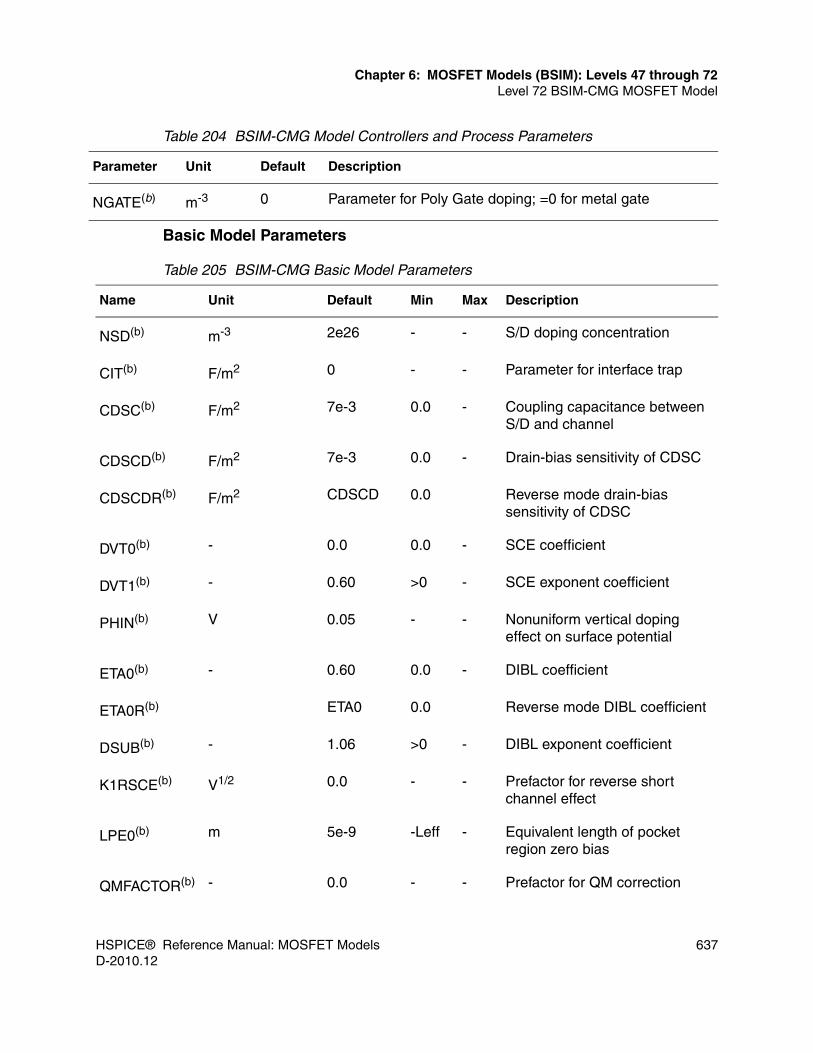
HSPICE® Reference Manual: MOSFET Models 637D-2010.12
Chapter 6: MOSFET Models (BSIM): Levels 47 through 72Level 72 BSIM-CMG MOSFET Model
Basic Model Parameters
NGATE(b) m-3 0 Parameter for Poly Gate doping; =0 for metal gate
Table 205 BSIM-CMG Basic Model Parameters
Name Unit Default Min Max Description
NSD(b) m-3 2e26 - - S/D doping concentration
CIT(b) F/m2 0 - - Parameter for interface trap
CDSC(b) F/m2 7e-3 0.0 - Coupling capacitance between S/D and channel
CDSCD(b) F/m2 7e-3 0.0 - Drain-bias sensitivity of CDSC
CDSCDR(b) F/m2 CDSCD 0.0 Reverse mode drain-bias sensitivity of CDSC
DVT0(b) - 0.0 0.0 - SCE coefficient
DVT1(b) - 0.60 >0 - SCE exponent coefficient
PHIN(b) V 0.05 - - Nonuniform vertical doping effect on surface potential
ETA0(b) - 0.60 0.0 - DIBL coefficient
ETA0R(b) ETA0 0.0 Reverse mode DIBL coefficient
DSUB(b) - 1.06 >0 - DIBL exponent coefficient
K1RSCE(b) V1/2 0.0 - - Prefactor for reverse short channel effect
LPE0(b) m 5e-9 -Leff - Equivalent length of pocket region zero bias
QMFACTOR(b) - 0.0 - - Prefactor for QM correction
Table 204 BSIM-CMG Model Controllers and Process Parameters
Parameter Unit Default Description

638 HSPICE® Reference Manual: MOSFET ModelsD-2010.12
Chapter 6: MOSFET Models (BSIM): Levels 47 through 72Level 72 BSIM-CMG MOSFET Model
VSAT(b) m/s 85000 - - Saturation velocity
KSATIV(b) - 1.3 - - Parameter for reverse short channel effect
MEXP(b) - 4 2 - Smoothing function factor for Vdsat
PTWG(b) v-2 0.0 - - Correction factor for velocity saturation
THETASAT(b) V-1 2.0 - - Velocity saturation parameter
U0(b) m2/V-s 6e-2 - - Low field mobility
ETAMOB(b) - 2.0 - - Effective field parameter
UP(b) 0.0 - - Mobility L coefficient
LPA - 1.0 - - Mobility L power coefficient
UA(b) (cm/MV)EU 0.3 >0.0 - MOBMOD = 0 phonon / surface roughness scattering
EU(b) cm/MV 2.5 >0.0 - MOBMOD = 0 phonon / surface roughness scattering
UD(b) cm/MV 0.0 >0.0 - MOBMOD = 0 Coulombic scattering (Experimental)
UCS(b) - 1.0 >0.0 - MOBMOD = 0 Coulombic scattering (Experimental)
MUE(b) cm/MV 1.2 >0.0 - MOBMOD=1 Mobility reduction coefficient
THETAMU - 1.0 >0.0 - MOBMOD = 1 mobility reduction exponent
CS(b) - 0.0 >0.0 - Coulombic scattering parameter
Table 205 BSIM-CMG Basic Model Parameters (Continued)
Name Unit Default Min Max Description
μmLPA

HSPICE® Reference Manual: MOSFET Models 639D-2010.12
Chapter 6: MOSFET Models (BSIM): Levels 47 through 72Level 72 BSIM-CMG MOSFET Model
ALP(b) - 0.013 - - CLMMOD = 0 Channel Length Modulation (CLM) prefactor
VP V 0.0 - - CLMMOD = 0 CLM log dependence parameter
PCLM(b) - 0.013 - - CLMMOD = 1 Channel Length Modulation parameter
PCLMG - 0 - - CLMMOD = 1 Gate bias dependent parameter for channel Length Modulation (CLM)
VASAT V 0.2 - - CLMMOD = 1 Channel Length Modulation (CLM) parameter
RDSWMIN 0.0 - - RDSMOD = 0 S/D extension resistance per unit width at high Vgs
RDSW(b) 40 0.0 - RDSMOD = 0 zero bias S/D extension resistance per unit width
RSWMIN 0.0 0.0 - RDSMOD = 1 source extension resistance per unit width at high Vgs
RSW(b) 50 0.0 - RDSMOD = 1 zero bias source extension resistance per unit width
RDWMIN 0.0 0.0 - RDSMOD = 1 drain extension resistance per unit width at high Vgs
RDW(b) 50 0.0 - RDSMOD = 1 zero bias drain extension resistance per unit width
Table 205 BSIM-CMG Basic Model Parameters (Continued)
Name Unit Default Min Max Description
Ω μWRm–
Ω μWRm–
Ω μmWR
–
Ω μmWR
–
Ω μmWR
–
Ω μmWR
–

640 HSPICE® Reference Manual: MOSFET ModelsD-2010.12
Chapter 6: MOSFET Models (BSIM): Levels 47 through 72Level 72 BSIM-CMG MOSFET Model
PRWG(b) V-1 0.0 0.0 - Gate bias dependence of S/D extension resistance
WR(b) - 1.0 - - W dependence parameter of S/D extension resistance
RGEXT 0.0 0.0 - Eective gate electrode external resistance (Experimental)
RGFIN 1.0e-3 1.0e-3 - Eective gate electrode resistance per n per finger
RSHS 0.0 0.0 - Source-side sheet resistance
RSHD RSHS 0.0 - Drain-side sheet resistance
PDIBL1 - 1.30 0.0 - Parameter for DIBL effect on Rout
PDIBL2 2e-4 0.0 - Parameter for DIBL effect on Rout
DROUT 1.06 >0.0 - 0.56
PVAG(b) - 1.0 - - Vgs dependence on early voltage
AIGBINV(b) 1.11e-2 - - Parameter for Igb in inversion
BIGBINV(b) 9.49e-4 - - Parameter for Igb in inversion (BULKMOD only)
CIGBINV(b) V-1 6.00e-3 - - Parameter for Igb in inversion (BULKMOD only)
EIGBINV(b) V 1.1 - - Parameter for Igb in inversion (BULKMOD only)
NIGBINV(b) - 3.0 > 0.0 - Parameter for Igb in inversion (BULKMOD only)
Table 205 BSIM-CMG Basic Model Parameters (Continued)
Name Unit Default Min Max Description
Ω
Ω
Ω
Ω
Fs2
g⁄( ) m0.5 1–
Fs2
g⁄( ) m0.5 1–
V1–

HSPICE® Reference Manual: MOSFET Models 641D-2010.12
Chapter 6: MOSFET Models (BSIM): Levels 47 through 72Level 72 BSIM-CMG MOSFET Model
AIGC(b) 1.36e-2 - - Parameter for Igc in inversion
BIGC(b) 1.71e-3 - - Parameter for Igc in inversion
CIGC(b) V -1 0.075 - - Parameter for Igc in inversion
NIGC(b) - 1 >0 - Parameter for Igc in inversion
DLCIGS m 0 - - Delta L for Igs model
AIGS(b) 1.36e2 - - Parameter for Igs in inversion
BIGS(b) 1.71e-3 - - Parameter for Igs in inversion
CIGS(b) V -1 0.075 - - Parameter for Igs in inversion
DLCIGD m DLCIGS - - Delta L for Igd model
AIGD(b) 1.36e2 - - Parameter for Igd in inversion
BIGD(b) 1.71e-3 - - Parameter for Igd in inversion
CIGD(b) V -1 0.075 - - Parameter for Igd in inversion
POXEDGE(b) - 1 >0 - Factor for the gate edge Tox
AGIDL(b) 6.055 - - Pre-exponential coefficient for GIDL
BGIDL(b) V/m 0.3e9 - - Exponential coefficient for GIDL
EGIDL(b) V 0.2 Band bending parameter for GIDL
AGISL(b) AIGDL - - Pre-exponential coefficient for GISL
Table 205 BSIM-CMG Basic Model Parameters (Continued)
Name Unit Default Min Max Description
Fs2
g⁄( ) m0.5 1–
Fs2
g⁄( ) m0.5 1–
V1–
Fs2
g⁄( ) m0.5 1–
Fs2
g⁄( ) m0.5 1–
V1–
Fs2
g⁄( ) m0.5 1–
Fs2
g⁄( ) m0.5 1–
V1–
Ω 1–
Ω 1–

642 HSPICE® Reference Manual: MOSFET ModelsD-2010.12
Chapter 6: MOSFET Models (BSIM): Levels 47 through 72Level 72 BSIM-CMG MOSFET Model
BGISL(b) V/m BIGDL Band bending parameter for GISL
EGISL(b) V EGIDL - - Pre-exponential coefficient for GISL
ALPHA0(b) 0.0 - - First parameter of Iii
ALPHA1(b) V -1 0.0 - - L scaling parameter of Iii
BETA0(b) V -1 0.0 - - Vds dependent parameter of Iii
ALPHAII(b) - 0.0 - - Pre-exponential constant for Iii (IIMOD=2)
BETAII0(b) V -1 0.0 - - Vds dependent parameter of Iii (IIMOD=2)
BETAII1(b) - 0.0 - - Vds dependent parameter of Iii (IIMOD=2)
BETAII2(b) V 0.0 - - Vds dependent parameter of Iii (IIMOD=2)
ESATII(b) V/m 1.0e7 - - Saturation channel E-Field for Iii (IIMOD=2)
LII(b) V -m 0.5e-9 - - Channel length dependent parameter of Iii (IIMOD=2)
SII0(b) V-1 0.0 - - Vgs dependent parameter of Iii (IIMOD=2)
SII1(b) - 0.0 - - Vgs dependent parameter of Iii (IIMOD=2)
SII2(b) V 0.0 - - Vgs dependent parameter of Iii (IIMOD=2)
SIID(b) V 0.0 - - Vds dependent parameter of Iii (IIMOD=2)
Table 205 BSIM-CMG Basic Model Parameters (Continued)
Name Unit Default Min Max Description
m V1–⋅

HSPICE® Reference Manual: MOSFET Models 643D-2010.12
Chapter 6: MOSFET Models (BSIM): Levels 47 through 72Level 72 BSIM-CMG MOSFET Model
LOVSb) m 1.0e-9 0.0 - Gate-to-source overlap length (for parasitic capacitance calculation)
LOVD(b) m LOVS 0.0 - Gate-to-drain overlap length (for parasitic capacitance calculation)
CFS(b) F/m 2.5e-11 0.0 - Source-side outer fringe cap (for parasitic capacitance calculation)
CFD(b) F/m CFS 0.0 - Drain-side outer fringe cap (for parasitic capacitance calculation)
COVS(b) F 0 0.0 - Constant gate-to-source overlap cap (for parasitic capacitance calculation)
COVD(b) F COVS 0.0 - Constant gate-to-drain overlap cap (for parasitic capacitance calculation)
CJS F/m2 0.003 0.0 - Unit area source-side junction capacitance at zero bias
CJD F/m2 CJS 0.0 - Unit area drain-side junction capacitance at zero bias
CJSWS1 F/m 3.0e-10 0.0 - 1st unit length source-side sidewall junction capacitance at zero bias
CJSWD1 F/m CJSWS1 0.0 - 1st unit length drain-side sidewall junction capacitance at zero bias
CJSWS2 F/m 3.0e-10 0.0 - 2nd unit length source-side sidewall junction capacitance at zero bias
Table 205 BSIM-CMG Basic Model Parameters (Continued)
Name Unit Default Min Max Description

644 HSPICE® Reference Manual: MOSFET ModelsD-2010.12
Chapter 6: MOSFET Models (BSIM): Levels 47 through 72Level 72 BSIM-CMG MOSFET Model
CJSWD2 F/m CJSWS1 0.0 - 2nd unit length drain-side sidewall junction capacitance at zero bias
PBS V 1.0 0.01 - Unit area source-side junction capacitance at zero bias
PBD V PBS 0.01 - Unit area drain-side junction capacitance at zero bias
PBSWS1 V 1.0 0.01 - Built-in potential for 1st source-side sidewall junction capacitance
PBSWD1 V PBSWS1 0.0 - Built-in potential for 1st drain-side sidewall junction capacitance
PBSWS2 V PBSWS1 0.01 - Built-in potential for 2nd source-side sidewall junction capacitance
PBSWD2 V PBSWS2 0.01 - Built-in potential for 2nd drain-side sidewall junction capacitance
MJS - 0.5 - - Source bottom junction capacitance grading coefficient
MJD - MJS - - Drain bottom junction capacitance grading coefficient
MJSWS1 - 0.33 1st source sidewall junction capacitance grading coefficient
MJSWD1 - MJSWS1 - - 2nd drain sidewall junction capacitance grading coefficient
MJSWS2 - MJSWS1 - - 2nd source sidewall junction capacitance grading coefficient
Table 205 BSIM-CMG Basic Model Parameters (Continued)
Name Unit Default Min Max Description

HSPICE® Reference Manual: MOSFET Models 645D-2010.12
Chapter 6: MOSFET Models (BSIM): Levels 47 through 72Level 72 BSIM-CMG MOSFET Model
MJSWD2 - MJSWS2 - - 2nd drain sidewall junction capacitance grading coefficient
JSS A/m2 1.0e-4 0.0 - Bottom source junction reverse saturation current density
JSD A/m2 JSS 0.0 - Bottom drain junction reverse saturation current density
JSWS1 A/m 0 0.0 0.0 Unit length reverse saturation current for 1st sidewall source junction
JSWD1 A/m JSWS1 0.0 0.0 Unit length reverse saturation current for 1st sidewall drain junction
JSWS2 A/m JSWS1 0.0 0.0 Unit length reverse saturation current for 2nd sidewall source junction
JSWD2 A/m JSWS2 0.0 0.0 Unit length reverse saturation current for 2nd sidewall drain junction
NJS - 1.0 0.0 - Source junction emission coefficient
NJD - NJS 0.0 - Drain junction emission coefficient
IJTHSFWD A 0.1 10 Isbs - Forward source diode breakdown limiting current
IJTHDFWD A IJTHSFWD 10 Isbs - Forward drain diode breakdown limiting current
IJTHSREV A 0.1 10 Isbs - Reverse source diode breakdown limiting current
IJTHDREV A IJTHSREV Reverse drain diode breakdown limiting current
Table 205 BSIM-CMG Basic Model Parameters (Continued)
Name Unit Default Min Max Description

646 HSPICE® Reference Manual: MOSFET ModelsD-2010.12
Chapter 6: MOSFET Models (BSIM): Levels 47 through 72Level 72 BSIM-CMG MOSFET Model
Parameters for Temperature Dependence and Self-Heating
BVS V 10.0 Source diode breakdown voltage
BVD V BVS Drain diode breakdown voltage
Table 206 BSIM-CMG Temperature Dependent and Self-Heating Parameters
Name Unit Default Min Max Description
TNOM 300.15 0.9 - Temperature at which the model is extracted
TBGASUB 7.02e-4 - - Bandgap temperature coefficient
TBGBSUB 1108.0 - - Bandgap temperature coefficient
KT1 V -0.3 - - Vth temperature coefficient
KT1L V m 0.0 - - Vth temperature coefficient
UTE(b) - -1.4 - - Mobility temperature coefficient
UA1(b) - -1.1 - - Mobility (MOBMOD=0) temperature coefficient
UD1(b) - 0.0 - - Mobility (MOBMOD=0) temperature coefficient (Experimental)
UCSTE(b) - -4.775e-3 - - Mobility (MOBMOD=0) temperature coefficient (Experimental)
STTHETAMU - 1.5 - - Mobility (MOBMOD=0) temperature coefficient
STMUE - 0.0 - - Mobility (MOBMOD=1) temperature coefficient
STCS - 0.0 - - Mobility (MOBMOD=1) temperature coefficient
Table 205 BSIM-CMG Basic Model Parameters (Continued)
Name Unit Default Min Max Description
° K
eV( ) ° K( )⁄
° K
⋅

HSPICE® Reference Manual: MOSFET Models 647D-2010.12
Chapter 6: MOSFET Models (BSIM): Levels 47 through 72Level 72 BSIM-CMG MOSFET Model
AT(b) 0.005 - - Saturation velocity temperature coefficient
TMEXP(b) 0 - - Temperature coefficient for
smoothing
PTWGT(b) 0.004 - - PTWG temperature coefficient
STTHETASAT - 1.0 - - Saturation velocity temperature coefficient
PRT(b) - 0.001 - - Series resistance temperature coefficient
IIT(b) - -0.5 - - Impact ionization temperature coefficient(IIMOD=1)
TII(b) - 0.0 - - Impact ionization temperature coefficient(IIMOD=2)
TGIDL(b) -0.003 - - GISL/GIDL temperature coefficient
IGT(b) - 2.5 - - Gate current temperature coefficient
TCJ 0.0 - - Temperature coefficient for cjs/cjd
TCJSW1 0.0 - - Temperature coefficient for cjsws1/cjdwd1
TCJSW2 0.0 - - Temperature coefficient for cjsws2/cjdwd2
TPB 0.0 - - Temperature coefficient for pbs/pbd
TPBSW1 0.0 - - Temperature coefficient for pbsws1/pbdwd1
TPBSW2 0.0 - - Temperature coefficient for pbsws2/pbdwd2
Table 206 BSIM-CMG Temperature Dependent and Self-Heating Parameters
Name Unit Default Min Max Description
1 ° K( )⁄
1 ° K( )⁄ Vdseff
1 ° K( )⁄
1 ° K( )⁄
1 ° K( )⁄
1 ° K( )⁄
1 ° K( )⁄
1 ° K( )⁄
1 ° K( )⁄
1 ° K( )⁄

648 HSPICE® Reference Manual: MOSFET ModelsD-2010.12
Chapter 6: MOSFET Models (BSIM): Levels 47 through 72Supported Instance Parameters, BSIM3, BSIM4, BSIM3SOI and BSIM4SOI
Supported Instance Parameters, BSIM3, BSIM4, BSIM3SOI and BSIM4SOI
The following lists the instance parameters that are currently supported by HSPICE in these four model types:
XTIS - 3.0 - - Drain junction current temperature exponent
XTID - XTIS - - Source junction current temperature exponent
RTH0 0.01 0.0 - Thermal resistance for self-heating calculation
CTH0 F 1.0e-5 0.0 - Thermal capacitance for self-heating calculation
WTH0 m 0.0 0.0 - Width-dependence coefficient for self-heating calculation
Table 207 Instance parameters: BSIM3,BSIM4, BSIM3SOI, BSIM4SOI
Instance Parameter BSIM3 BSIM4 BSIM3SOI BSIM4SOI
ACNQSMOD yes yes no no
AD yes yes yes yes
AS yes yes yes yes
CTH0 yes no yes yes
DELDVT0 no yes no no
DELK1 yes yes no yes
DELK2 no yes yes no
DELNFCT yes yes no yes
DELLPE0 no yes no no
DELRSH no yes no no
Table 206 BSIM-CMG Temperature Dependent and Self-Heating Parameters
Name Unit Default Min Max Description
Ω
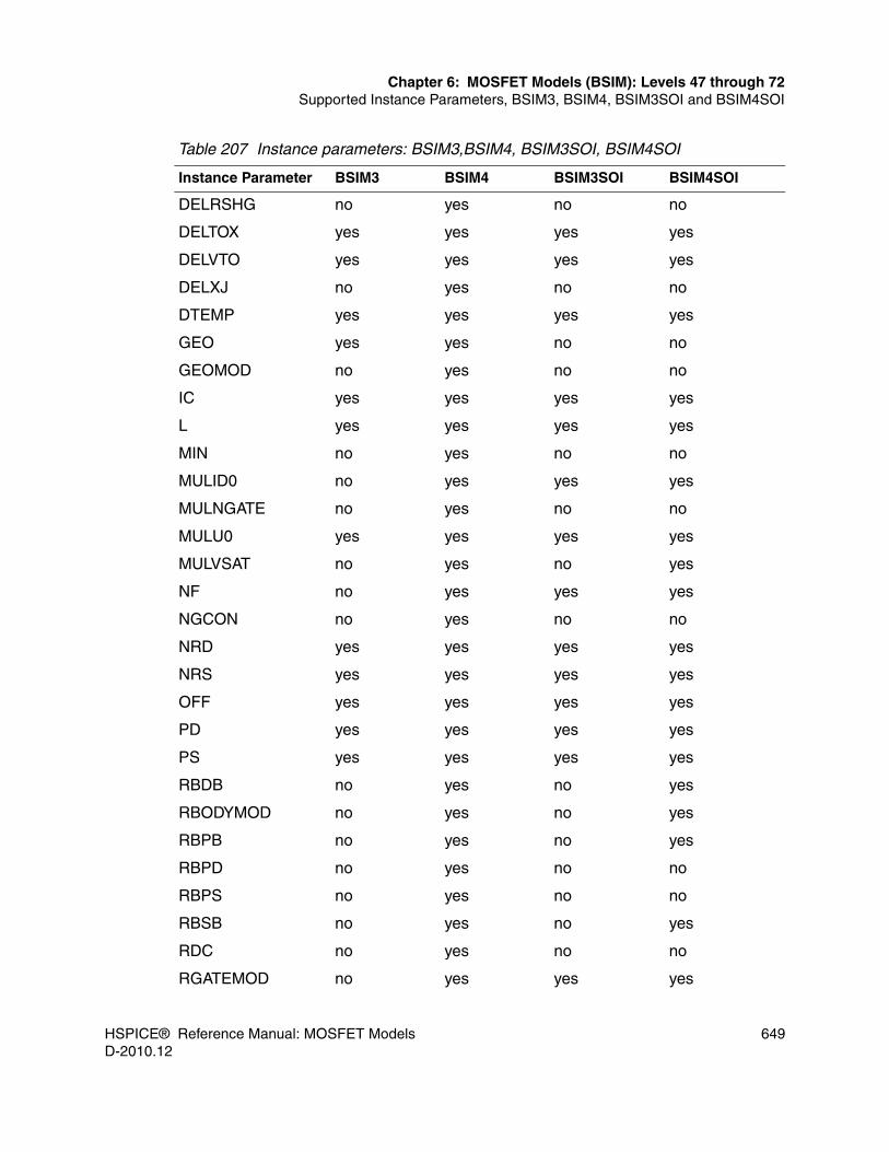
HSPICE® Reference Manual: MOSFET Models 649D-2010.12
Chapter 6: MOSFET Models (BSIM): Levels 47 through 72Supported Instance Parameters, BSIM3, BSIM4, BSIM3SOI and BSIM4SOI
DELRSHG no yes no no
DELTOX yes yes yes yes
DELVTO yes yes yes yes
DELXJ no yes no no
DTEMP yes yes yes yes
GEO yes yes no no
GEOMOD no yes no no
IC yes yes yes yes
L yes yes yes yes
MIN no yes no no
MULID0 no yes yes yes
MULNGATE no yes no no
MULU0 yes yes yes yes
MULVSAT no yes no yes
NF no yes yes yes
NGCON no yes no no
NRD yes yes yes yes
NRS yes yes yes yes
OFF yes yes yes yes
PD yes yes yes yes
PS yes yes yes yes
RBDB no yes no yes
RBODYMOD no yes no yes
RBPB no yes no yes
RBPD no yes no no
RBPS no yes no no
RBSB no yes no yes
RDC no yes no no
RGATEMOD no yes yes yes
Table 207 Instance parameters: BSIM3,BSIM4, BSIM3SOI, BSIM4SOI
Instance Parameter BSIM3 BSIM4 BSIM3SOI BSIM4SOI

650 HSPICE® Reference Manual: MOSFET ModelsD-2010.12
Chapter 6: MOSFET Models (BSIM): Levels 47 through 72Supported Instance Parameters, BSIM3, BSIM4, BSIM3SOI and BSIM4SOI
RGEOMOD no yes no no
RSC no yes no no
RTH0 yes no no no
SA yes yes no yes
SA1 yes yes no no
SA10 yes yes no no
SA2 yes yes no no
SA3 yes yes no no
SA4 yes yes no no
SA5 yes yes no no
SA6 yes yes no no
SA7 yes yes no no
SA8 yes yes no no
SA9 yes yes no no
SB yes yes no yes
SB1 yes yes no no
SB10 yes yes no no
SB2 yes yes no no
SB3 yes yes no no
SB4 yes yes no no
SB5 yes yes no no
SB6 yes yes no no
SB7 yes yes no no
SB8 yes yes no no
SB9 yes yes no no
SC 3.22 or later yes no no
SCA 3.22 or later yes no no
SCB 3.22 or later yes no no
SCC 3.22 or later yes no no
Table 207 Instance parameters: BSIM3,BSIM4, BSIM3SOI, BSIM4SOI
Instance Parameter BSIM3 BSIM4 BSIM3SOI BSIM4SOI

HSPICE® Reference Manual: MOSFET Models 651D-2010.12
Chapter 6: MOSFET Models (BSIM): Levels 47 through 72Supported Instance Parameters, BSIM3, BSIM4, BSIM3SOI and BSIM4SOI
SD yes yes no yes
SOIQ0 no no yes yes
STIMOD yes yes no no
SW1 yes yes no no
SW10 yes yes no no
SW2 yes yes no no
SW3 yes yes no no
SW4 yes yes no no
SW5 yes yes no no
SW6 yes yes no no
SW7 yes yes no no
SW8 yes yes no no
SW9 yes yes no no
TNODEOUT yes no yes yes
TRNQSMOD no yes no no
W yes yes yes yes
XGW no yes no no
Table 207 Instance parameters: BSIM3,BSIM4, BSIM3SOI, BSIM4SOI
Instance Parameter BSIM3 BSIM4 BSIM3SOI BSIM4SOI

652 HSPICE® Reference Manual: MOSFET ModelsD-2010.12
Chapter 6: MOSFET Models (BSIM): Levels 47 through 72Supported Instance Parameters, BSIM3, BSIM4, BSIM3SOI and BSIM4SOI

HSPICE® Reference Manual: MOSFET Models 653D-2010.12
7
7MOSFET Capacitance Models
This chapter discusses use of available capacitance models.
HSPICE ships hundreds of examples for your use; see Listing of Demonstration Input Files for paths to demo files.
These topics are presented in the following sections:■ MOS Gate Capacitance Models■ Selecting Capacitor Models■ Transcapacitance■ Operating Point Capacitance Printout■ Element Template Printout■ Calculating Gate Capacitance■ MOS Gate Capacitance Model Parameters■ Specifying XQC and XPART for CAPOP=4, 9, 11, 12, 13■ Overlap Capacitance Equations■ CAPOP=0 — SPICE Meyer Gate Capacitances■ CAPOP=1 — Modified Meyer Gate Capacitances■ CAPOP=3 — Gate Capacitances (Simpson Integration)■ CAPOP=4—Charge Conservation Capacitance Model■ CAPOP=5 — No Gate Capacitance■ CAPOP=6 — AMI Gate Capacitance Model■ CAPOP=13 — BSIM1-based Charge-Conserving Gate Capacitance Model

654 HSPICE® Reference Manual: MOSFET ModelsD-2010.12
Chapter 7: MOSFET Capacitance ModelsMOS Gate Capacitance Models
■ CAPOP=39 — BSIM2 Charge-Conserving Gate Capacitance Model■ Calculating Effective Length and Width for AC Gate Capacitance
MOS Gate Capacitance Models
You can use capacitance model parameters with all MOSFET model statements.
Three fixed-capacitance parameters (CGDO, CGSO, and CGBO) represent gate-to-drain, gate-to-source, and gate-to-bulk overlap capacitances to model charge storage, use fixed and nonlinear gate capacitances and junction capacitances. The algorithm used for calculating nonlinear, voltage-dependent MOS gate capacitance depends on the value of the CAPOP model parameter.
To model MOS gate capacitances as a nonlinear function of terminal voltages, use Meyer’s piecewise linear model for all MOS levels. The charge conservation model is also available for MOSFET model Levels 2 through 7, 13, and 27. For LEVEL 1, you must specify the TOX model parameter to invoke the Meyer model. The next three sections describe the Meyer, Modified Meyer, and Charge Conservation MOS Gate Capacitance models.
Some of the charge conserving models (Ward-Dutton or BSIM) can cause “timestep too small” errors if you do not specify other nodal capacitances.
Selecting Capacitor Models
When you select a gate capacitance model, you can choose various combinations of capacitor models and DC models. You can incrementally update older DC models with new capacitance equations, without having to move to a new DC model. You can use the CAPOP model parameter to select the gate capacitance and validate the effects of different capacitance models.
The CAPOP capacitance model selection parameter selects the capacitor models to use for modeling the MOS gate capacitance: ■ gate-to-drain capacitance■ gate-to- source capacitance■ gate-to-bulk capacitance.

HSPICE® Reference Manual: MOSFET Models 655D-2010.12
Chapter 7: MOSFET Capacitance ModelsSelecting Capacitor Models
You can use CAPOP to select several versions of the Meyer and charge conservation model.
Some capacitor models are tied to specific DC models (DC model level in parentheses below). Other models are designated as general; any DC model can use them.
Parameter Description
CAPOP=0 SPICE original Meyer gate-capacitance model (general)
CAPOP=1 Modified Meyer gate-capacitance model (general)
CAPOP=2 Parameterized Modified Meyer gate-capacitance model (general default)
CAPOP=3 Parameterized Modified Meyer gate-capacitance model with Simpson integration (general)
CAPOP=4 Charge conservation capacitance model (analytic), Levels 2, 3, 6, 7, 13, 28, and 39 only
CAPOP=5 No capacitor model
CAPOP=6 AMI capacitor model (LEVEL 5)
CAPOP=9 Charge conservation model (LEVEL 3)
CAPOP=11 Ward-Dutton model (specialized, LEVEL 2)
CAPOP=12 Ward-Dutton model (specialized, LEVEL 3)
CAPOP=13 Generic BSIM Charge-Conserving Gate Capacitance model (default for Levels 13, 28, 39)
CAPOP=39 BSIM2 Charge-Conserving Gate Capacitance model (LEVEL 39)

656 HSPICE® Reference Manual: MOSFET ModelsD-2010.12
Chapter 7: MOSFET Capacitance ModelsTranscapacitance
CAPOP=4 selects the recommended charge-conserving model from among CAPOP=11, 12, or 13 for the specified DC model.
The proprietary models (Levels 5, 17, 21, 22, 25, 31, 33), the SOS model (LEVEL 27), and models higher than 49 have their own built-in capacitance routines.
Transcapacitance
If a capacitor has two terminals (1 and 2) with charges named Q1 and Q2 on the two terminals that sum to zero (for example, Q1=-Q2), then the charge is a function of the voltage difference between the terminals (V12=V1-V2). One quantity (C=dQ1/dV12) completely describes the small-signal characteristics of the device.
If a capacitor has four terminals, the sum of the charges on the four terminals must equal zero (Q1+Q2+Q3+Q4=0). They can depend only on voltage differences, but they are otherwise arbitrary functions. Because three independent charges (Q1, Q2, Q3) are functions of three independent voltages (V14, V24, V34), you must specify nine derivatives to describe the small-signal characteristics.
You can consider the four charges separately as functions of the four terminal voltages, Q1(V1,V2,V3,V4), ... Q4(V1,V2,V3,V4). The derivatives form a four-by-four matrix, dQi/dVj, i=1,.4, j=1,.4. Simulation directly interprets this matrix as AC measurements.
If you apply an AC voltage signal to the j terminal and you ground the other terminals to AC, and if you measure AC current into the i terminal, then the current is the imaginary constant times 2*pi*frequency times dQi/dVj.
Table 208 CAPOP = 4 Selections
MOS Level Default CAPOP CAPOP=4 selects
2 2 11
3 2 12
13, 28, 39 13 13
Other levels 2 11

HSPICE® Reference Manual: MOSFET Models 657D-2010.12
Chapter 7: MOSFET Capacitance ModelsTranscapacitance
■ Because the charges add up to zero, each column of this matrix must add up to zero.
■ Because the charges can depend only on voltage differences, each row must add up to zero.
In general, the matrix is not symmetrical:
dQi/dVj need not equal dQj/dVi
This is not an expected event because it does not occur for the two-terminal case. For two terminals, because the rows and columns must add up to zero, dQ1/dV2 must equal dQ2/dV1.
,
For three or more terminals, this relation does not generally hold.
The terminal input capacitances are the diagonal matrix entries:
Cii = dQi/dVi i=1,.4
The transcapacitances are the negative of off-diagonal entries:
Cij = -dQi/dVj i not equal to j
All of the C values are normally positive.
Figure 20 MOS Capacitances
dQ1dV1----------- dQ2
dV1-----------+ 0=
dQ1dV1----------- dQ1
dV2-----------+ 0=
Gate
Source
CDG
CGD
CGG
CSS
CBB
CGBCBG
DrainCDD
CSG
CGS
CDB
CBD
CSB
CBS

658 HSPICE® Reference Manual: MOSFET ModelsD-2010.12
Chapter 7: MOSFET Capacitance ModelsOperating Point Capacitance Printout
In Figure 20, Cij determines the current transferred out of the i node from a voltage change on the j node. The arrows, representing direction of influence, point from node j to node i.
A MOS device with terminals named D, G, S, and B provides:
, ,
■ CGG represents input capacitance: a change in gate voltage requires a current equal to CGGxdVG/dt into the gate terminal.
■ CGD represents Miller feedback: a change in drain voltage creates a current equal to CGGxdVG/dt out of the gate terminal.
■ CDG represents Miller feedthrough, capacitive current out of the drain due to a change in gate voltage.
To show how CGD might not equal CDG, the following example is a simplified model with no bulk charge with a gate charge as a function of VGS only, and with the 50/50 channel charge partitioned into QS and QD:
, , ,
Consequently:
,
Therefore, this model has Miller feedthrough, but no feedback.
Operating Point Capacitance Printout
The operating point printout reports six capacitances:
Table 209 Operating Point Capacitance
Capacitance Value
cdtot dQD/dVD
cgtot dQG/dVG
cstot dQS/dVS
cbtot dQB/dVB
CGGdQgdVG-----------= CGD
dQgdVD-----------–= CDG
dQDdVG------------–=
QG Q vgs( )= QS 0.5– Q vgs( )⋅= QD 0.5– Q vgs( )⋅= QB 0=
CGDdQGdVD------------– 0= = CDG
dQDdVG------------– 0.5
dQdvgs------------⋅= =

HSPICE® Reference Manual: MOSFET Models 659D-2010.12
Chapter 7: MOSFET Capacitance ModelsElement Template Printout
These capacitances include gate-drain, gate-source, and gate-bulk overlap capacitance, and drain-bulk and source-bulk diode capacitance. Drain and source refer to node 1 and 3 of the MOS element (physical instead of electrical).
For the Meyer models, where charges such as QD are not well defined, Table 210 shows the printout quantities.
Element Template Printout
The MOS element template printouts for gate capacitance are LX18 to LX23 and LX32 to LX34. From these nine capacitances, you can construct the complete four-by-four matrix of transcapacitances. The nine LX printouts are:
cgs -dQG/dVS
cgd -dQG/dVD
Table 210 Capacitance Printout for Meyer Models
Capacitance Value
cdtot cgd+cdb
cgtot cgs+cgd+cgb
cstot cgs+csb
cbtot cgb+csb+cdb
cgs cgs
cgd cgd
Table 209 Operating Point Capacitance
Capacitance Value

660 HSPICE® Reference Manual: MOSFET ModelsD-2010.12
Chapter 7: MOSFET Capacitance ModelsElement Template Printout
LX18(m) = dQG/dVGB = CGGBOLX19(m) = dQG/dVDB = CGDBOLX20(m) = dQG/dVSB = CGSBOLX21(m) = dQB/dVGB = CBGBOLX22(m) = dQB/dVDB = CBDBOLX23(m) = dQB/dVSB = CBSBOLX32(m) = dQD/dVG = CDGBOLX33(m) = dQD/dVD = CDDBOLX34(m) = dQD/dVS = CDSBO
These capacitances include gate-drain, gate-source, and gate-bulk overlap capacitance, and drain-bulk and source-bulk diode capacitance. Drain and source refer to node 1 and 3 of the MOS element (physical instead of electrical).
For an NMOS device with source and bulk grounded:■ LX18 is the input capacitance.■ LX33 is the output capacitance.■ LX19 is the Miller feedback capacitance (gate current induced by voltage
signal on the drain).■ LX32 is the Miller feedthrough capacitance (drain current induced by the
voltage signal on the gate).
A device operating with node 3 as electrical drain—for example an NMOS device with node 3 at higher voltage than node 1—is in reverse mode.
The LX values are physical, but you can translate them into electrical definitions by interchanging D and S:
CGG(reverse) = CGG = LX18CDD(reverse) = CSS = dQS/dVS = d(-QG-QB-QD)/dVS =
-LX20-LX23-LX34CGD(reverse) = CGS = -LX20CDG(reverse) = CSG = -dQS/dVG = d(QG+QB+QD)/dVG =
LX18+LX21+LX32
For Meyer models, QD and other charges are not well defined. The formulas (such as LX18= CGG, LX19= -CGD) are still true, but the transcapacitances are symmetrical; for example, CGD=CDG. In terms of the six independent Meyer capacitances (cgd, cgs, cgb, cdb, csb, and cds), the LX printouts are:

HSPICE® Reference Manual: MOSFET Models 661D-2010.12
Chapter 7: MOSFET Capacitance ModelsCalculating Gate Capacitance
LX18(m) = CGS+CGD+CGBLX19(m) = LX32(m) = -CGDLX20(m) = -CGSLX21(m) = -CGB LX22(m) = -CDBLX23(m) = -CSBLX33(m) = CGD+CDB+CDSLX34(m) = -CDS
Calculating Gate Capacitance
The following input file example shows a gate capacitance calculation in detail
for a BSIM model. TOX is chosen so that:
In this example, Vfb0, phi, and k1 are chosen so that vth=1v. The AC sweep is
chosen so that the last point is:
Input FileThis example is based on demonstration netlist calcap.sp, which is available in directory $<installdir>/demo/hspice/mos:
$m d g 0 b nch l=0.8u w=100u ad=200e-12 as=200e-12vd d 0 5vg g 0 5 ac 1vb b 0 0.ac dec 1 1.59155e4 1.59155e5.print CGG=lx18(m) CDD=lx33(m) CGD=par('-lx19(m)')+ CDG=par('-lx32(m)').print ig_imag=ii2(m) id_imag=ii1(m).model nch nmos level=13 update=2+ xqc=0.6 toxm=345.315 vfb0=-1 phi0=1 k1=1.0 muz=600+ mus=650 acm=2+ xl=0 ld=0.1u meto=0.1u cj=0.5e-4 mj=0 cjsw=0.altervd d 0 5 ac 1vg g 0 5.end
eoxtox--------- 1e 3F m
2⁄–=
2 π freq⋅ ⋅ 1e6s1–
=

662 HSPICE® Reference Manual: MOSFET ModelsD-2010.12
Chapter 7: MOSFET Capacitance ModelsCalculating Gate Capacitance
Calculations
BSIM equations for internal capacitance in saturation with xqc=0.4:
Gate-drain overlap =
Adding the overlaps:
Drain-bulk diode cap =
Adding the diodes:
Leff 0.6u=
eoxtox--------- 1e 3F m
2⁄–=
CapLeff Weff eox⋅ ⋅
tox---------------------------------------------- 60e 15F–= =
body 1 0.5+ 11
1.744 0.8364+ PHI0 vsb+( )⋅( )----------------------------------------------------------------------------------–⎝ ⎠
⎛ ⎞ K1
PHI0 vsb+( )--------------------------------------⋅ ⋅=
1 0.5+ 11
1.744 0.8364+( )-----------------------------------------–⎝ ⎠
⎛ ⎞⋅ 1.3062=
cgg Cap 11
3 body⋅( )---------------------------–⎝ ⎠
⎛ ⎞⋅ Cap 0.7448⋅ 44.69F= = =
cgd 0=
cdg415------⎝ ⎠
⎛ ⎞ Cap⋅ 16F= =
cdd 0=
ld meto+( ) Weffeoxtox---------⋅ ⋅ 20e 15F–=
cgg 44.69F 2 20F⋅+ 84.69F= =
cgd 20F=
cdg 36F=
cdd 20F=
cj ad⋅ 0.5e 4–( ) 200e 12–( )⋅ 10F= =
cgg 84.69F=

HSPICE® Reference Manual: MOSFET Models 663D-2010.12
Chapter 7: MOSFET Capacitance ModelsCalculating Gate Capacitance
Resultssubcktelement 0:m model 0:nch cdtot 30.0000fcgtot 84.6886fcstot 65.9999fcbtot 43.4213fcgs 61.2673fcgd 20.0000f
The calculation and simulation results match.
Plotting Gate CapacitancesThe following input file shows how to plot gate capacitances as a function of bias. Set .OPTION DCCAP to turn on capacitance calculations for a DC sweep. The model used is the same as for the previous gate capacitance calculations.
ExampleThis example is based on demonstration netlist gatecap.sp, which is available in directory $<installdir>/demo/hspice/mos:
cgd 20F=
cdg 36F=
cdd 30F=

664 HSPICE® Reference Manual: MOSFET ModelsD-2010.12
Chapter 7: MOSFET Capacitance ModelsCalculating Gate Capacitance
$ gate capacitance plots.option dccap=1 postm d g 0 b nch l=0.8u w=100u ad=200e-12 as=200e-12vd d 0 0vg g 0 5vb b 0 0.dc vd 0 5 .1.print vds=v(d) CGG=lx18(m)+ CGD=par('-lx19(m)') CDG=par('-lx32(m)')+ CGS=par('-lx20(m)') CSG=par('lx18(m)+lx21(m)+lx32(m)')+ CGB=par('lx18(m)+lx19(m)+lx20(m)') CBG=par('-lx21(m)').model nch nmos+ level=13 update=2 xqc=0.6 toxm=345.315+ vfb0=-1 phi0=1 k1=1.0 muz=600 mus=650+ acm=2 xl=0 ld=0.1u meto=0.1u+.end
Figure 21 Gate Capacitance
100.0F
1.0PDN [Lin]
LD [L
in]
CJPLOT.AS0C0
90.0F
80.0F
70.0F
60.0F
50.0F
40.0F
30.0F
20.0F
10.0F
02.0 3.0 4.0 5.0
CDB
CDB
CDB
CDB
CDB
CDB
0

HSPICE® Reference Manual: MOSFET Models 665D-2010.12
Chapter 7: MOSFET Capacitance ModelsCalculating Gate Capacitance
Capacitance Control OptionsThe SCALM, CVTOL, DCSTEP, and DCCAP control options affect the CAPOP models. ■ SCALM scales the model parameters (ignored in Levels 49 and higher).■ CVTOL controls the error tolerance for convergence for the CAPOP=3 model
(see CAPOP=3 — Gate Capacitances (Simpson Integration) on page 681). ■ DCSTEP models capacitances with a conductance during DC analysis.
■ DCCAP calculates capacitances in DC analysis.
Scaling.OPTION SCALM scales the CGBO, CGDO, CGSO, COX, LD, and WD parameters according to fixed rules, which are a function of the parameter’s units. If the model parameter’s units are in meters, simulation multiplies the parameter by SCALM. For example:■ The LD parameter uses units in meters; to obtain its scaled value, simulation
multiplies the value of LD by SCALM. ■ If the units are in meters squared, simulation multiplies the parameter by
SCALM2. ■ If the units are in reciprocal meters, the parameter’s value is divided by
SCALM. For example, because CGBO is in farads/meter, the value of CGBO is divided by SCALM.
■ If the units are in reciprocal meters squared, then the parameter is divided by SCALM2.
For the scaling equations specific to each CAPOP level, see the individual CAPOP subsections.

666 HSPICE® Reference Manual: MOSFET ModelsD-2010.12
Chapter 7: MOSFET Capacitance ModelsMOS Gate Capacitance Model Parameters
MOS Gate Capacitance Model Parameters
Table 211 Basic Gate Capacitance Parameters
Name (Alias) Units Default Description
CAPOP - 2.0 Capacitance model selector.
COX (CO) F/m2 3.453e-4 Oxide capacitance. If you do not specify COX, simulation calculates it from TOX. The default corresponds to the TOX default of 1e-7:
COXscaled = COX/SCALM2
TOX m 1e-7 Oxide thickness, calculated from COX (if you specify COX). The program uses the default if you do not specify COX. For TOX>1, simulation assumes that the unit is Angstroms. A level-dependent default can override it. See specific MOSFET levels in this manual.
Table 212 Gate Overlap Capacitance Model Parameters
Name (Alias) Units Default Description
CGBO (CGB) F/m 0.0 Gate-bulk overlap capacitance per meter channel length. If you set WD and TOX, but you do not set CGBO, then simulation calculates CGBO.
CGBOscaled = CGBO/SCALM
CGDO (CGD, C2) F/m 0.0 Gate-drain overlap capacitance per meter channel width. If you set LD or METO and TOX, but you do not set CGDO, then simulation calculates CGDO.
CGDOscaled = CGDO/SCALM

HSPICE® Reference Manual: MOSFET Models 667D-2010.12
Chapter 7: MOSFET Capacitance ModelsMOS Gate Capacitance Model Parameters
CGSO (CGS, C1) F/m 0.0 Gate-source overlap capacitance per meter channel width. If you set LD or METO and TOX, but you do not set CGSO, then simulation calculates CGSO.
CGSOscaled = CGSO/SCALM
LD (LATD, DLAT) m Lateral diffusion into channel from source and drain diffusion.■ If you do not specify either LD or XJ,
then the LD default=0.0. ■ If you specify XJ but you do not specify
LD, then simulation calculates LD from XJ.
■ LD default=0.75 ⋅ XJ for all levels except LEVEL 4 for which LD default=0.75.
LDscaled = LD ⋅ SCALMLEVEL 4: LDscaled = LD ⋅ XJ ⋅ SCALM
METO m 0.0 Fringing field factor for gate-to-source and gate-to-drain overlap capacitance calculation.
METOscaled = METO ⋅ SCALM
WD m 0.0 Lateral diffusion into channel from bulk along width.
WDscaled = WD ⋅ SCALM
Table 212 Gate Overlap Capacitance Model Parameters
Name (Alias) Units Default Description

668 HSPICE® Reference Manual: MOSFET ModelsD-2010.12
Chapter 7: MOSFET Capacitance ModelsMOS Gate Capacitance Model Parameters
Table 213 Meyer Capacitance Parameters CAPOP=0, 1, 2
Name (Alias) Units Default Description
CF1 V 0.0 Modified MEYER control for transition of cgs from depletion to weak inversion for CGSO (for CAPOP=2 only)
CF2 V 0.1 Modified MEYER control for transition of cgs from weak to strong inversion region (for CAPOP=2 only)
CF3 1.0 Modified MEYER control for the cgs and cgd transition from the saturation region to the linear region as a function of vds (for CAPOP=2 only)
CF4 50.0 Modified MEYER control for the contour of the cgb and cgs smoothing factors
CF5 0.667 Modified MEYER control for the capacitance multiplier for cgs in the saturation region
CF6 500.0 Modified MEYER control for contour of cgd smoothing factor
CGBEX 0.5 cgb exponent (for CAPOP=1 only)
Table 214 Charge Conservation Parameters (CAPOP=4)
Name (Alias) Units Default Description
XQC 0.5 Coefficient of channel charge share attributed to drain; its range is 0.0 to 0.5. This parameter applies only to CAPOP=4 and some of its level-dependent aliases.
HSPICE® Reference Manual: MOSFET Models 669D-2010.12
Chapter 7: MOSFET Capacitance ModelsSpecifying XQC and XPART for CAPOP=4, 9, 11, 12, 13
Specifying XQC and XPART for CAPOP=4, 9, 11, 12, 13
Parameter rules for the gate capacitance charge sharing coefficient (XQC & XPART) in the saturation region:■ If you do not specify either XPART or XQC, then simulation uses the 0/100
model.■ If you specify both XPART and XQC, then XPART overrides XQC.■ If you specify XPART, but you do not specify XQC, then:
• XPART=0 → 40/60
• XPART=0.4 → 40/60
• XPART=0.5 → 50/50
• XPART=1 → 0/100
• XPART = any other value less than 1 → 40/60
• XPART >1 → 0/100If XQC is specified:■ If you specify XQC but you do not specify XPART, then:
• XQC=0 → 0/100
• XQC=0.4 → 40/60
• XQC=0.5 → 50/50
• XQC=1 → 0/100
• XQC = any other value less than 1 → 40/60
• XQC>1 → 0/100
The only difference is the treatment of the 0 parameter value.
After you specify XPART/XQC, the gate capacitance ramps from 50/50 at Vds=0 volt (linear region) to the value (with Vds sweep) in the saturation region in XPART/XQC. Ramping the charge-sharing coefficient ensures smooth gate capacitance characteristics.
Overlap Capacitance Equations
The overlap capacitors are common to all models. You can input them explicitly or the program can calculate them. Either way, these overlap capacitors must

670 HSPICE® Reference Manual: MOSFET ModelsD-2010.12
Chapter 7: MOSFET Capacitance ModelsCAPOP=0 — SPICE Meyer Gate Capacitances
be added into the respective voltage-variable capacitors before integration, and before the DC operating point reports the combined parallel capacitance.
Gate-to-Bulk Overlap Capacitance
If you specify CGBO, then:
Otherwise:
Gate-to-Source Overlap Capacitance
If you specify CGSO, then:
Otherwise:
Gate-to-Drain Overlap Capacitance
If you specify CGDO, then:
Otherwise:
Simulation calculates the Leff value for each model differently, and saves this value in the corresponding model section. The Weff calculation is not the same as the Weff value in the LEVEL 1, 2, 3, 6, 7 and 13 models.
The 2⋅ WDscaled factor is not subtracted.
CAPOP=0 — SPICE Meyer Gate Capacitances
Definition:
Gate-Bulk Capacitance (cgb)
Accumulation, vgs ≤ vth-PH1:
Depletion, vgs < vth:
Strong Inversion, vgs ≥ vth:
CGBOeff M Leff CGBOscaled⋅ ⋅=
CGBOeff 2 WDscaled Leff COXscaled M⋅ ⋅ ⋅ ⋅=
CGSOeff Weff CGSOscaled⋅=
CGSOeff Weff LDscaled METOscaled+( ) COXscaled⋅ ⋅=
CGDOeff Weff CGDOscaled⋅=
CGDOeff Weff LDscaled METOscaled+( ) COXscaled⋅ ⋅=
Weff M Wscaled WMLT⋅ XWscaled+( )⋅=
cap COXscaled Weff Leff⋅ ⋅=
cgb cap=
cgb capvth vgs–
PH1----------------------⋅=
cgb 0=

HSPICE® Reference Manual: MOSFET Models 671D-2010.12
Chapter 7: MOSFET Capacitance ModelsCAPOP=0 — SPICE Meyer Gate Capacitances
Gate-Source Capacitance (cgs)
Accumulation:
Depletion, vgs ≤ vth:
Strong Inversion Saturation Region: vgs > vth and vds ≥ vdsat
Strong Inversion Linear Region: vgs > vth and vds < vdsat
Gate-Drain Capacitance (cgd)The gate-drain capacitance has value only in the linear region.
Strong Inversion Linear Region: vgs > vth and vds < vdsat
ExampleThis example is based on demonstration netlist capop0.sp, which is available in directory $<installdir>/demo/hspice/mos:
vgs vthPHI
2----------–≤
cgs 0=
cgs CF5 cap⋅ cap vgs cth–( )⋅0.75 PHI⋅
--------------------------------------------+=
cgs CF5 cap⋅=
cgs CF5 cap 1vdsat vds–
2 vdsat vsb+( )⋅ vds– vsb–-------------------------------------------------------------------------
2–
⎩ ⎭⎨ ⎬⎧ ⎫
⋅ ⋅=
cgd CF5 cap 1vdsat vsb+
2 vdsat vsb+( )⋅ vds– vsb–-------------------------------------------------------------------------
2–
⎩ ⎭⎨ ⎬⎧ ⎫
⋅ ⋅=
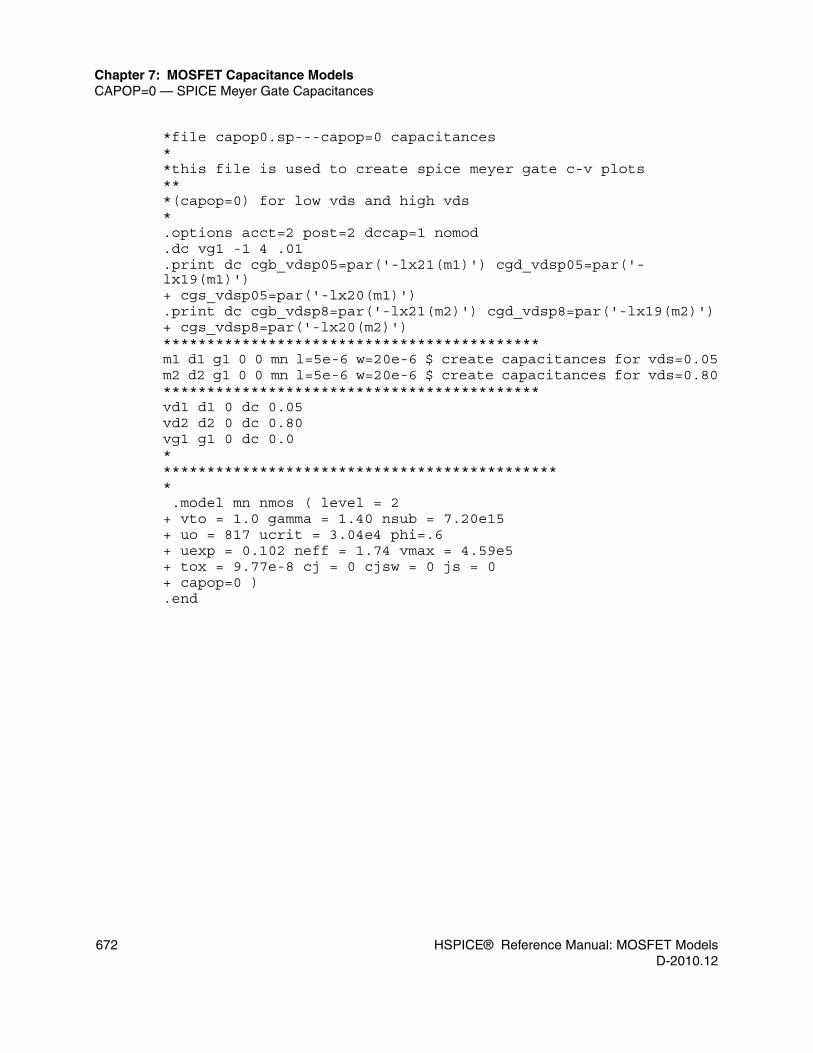
672 HSPICE® Reference Manual: MOSFET ModelsD-2010.12
Chapter 7: MOSFET Capacitance ModelsCAPOP=0 — SPICE Meyer Gate Capacitances
*file capop0.sp---capop=0 capacitances**this file is used to create spice meyer gate c-v plots***(capop=0) for low vds and high vds*.options acct=2 post=2 dccap=1 nomod.dc vg1 -1 4 .01.print dc cgb_vdsp05=par('-lx21(m1)') cgd_vdsp05=par('-lx19(m1)')+ cgs_vdsp05=par('-lx20(m1)').print dc cgb_vdsp8=par('-lx21(m2)') cgd_vdsp8=par('-lx19(m2)')+ cgs_vdsp8=par('-lx20(m2)')*******************************************m1 d1 g1 0 0 mn l=5e-6 w=20e-6 $ create capacitances for vds=0.05m2 d2 g1 0 0 mn l=5e-6 w=20e-6 $ create capacitances for vds=0.80*******************************************vd1 d1 0 dc 0.05vd2 d2 0 dc 0.80vg1 g1 0 dc 0.0*********************************************** .model mn nmos ( level = 2+ vto = 1.0 gamma = 1.40 nsub = 7.20e15+ uo = 817 ucrit = 3.04e4 phi=.6+ uexp = 0.102 neff = 1.74 vmax = 4.59e5+ tox = 9.77e-8 cj = 0 cjsw = 0 js = 0+ capop=0 ).end

HSPICE® Reference Manual: MOSFET Models 673D-2010.12
Chapter 7: MOSFET Capacitance ModelsCAPOP=1 — Modified Meyer Gate Capacitances
Figure 22 CAPOP=0 Capacitances
CAPOP=1 — Modified Meyer Gate Capacitances
Define:
In the following equations, G-, G+, D-, and D+ are smooth factors. You cannot change the values of these parameters.
Gate-Bulk Capacitance (cgb)Accumulation, vgs ≤ vfb – vsb
Depletion, vgs ≤ vth
50.0F
2.0Volts [Lin]
Par
am [L
in]
CAPOP0.SV0C68.VOSP05
3.0 4.01.0-1.0 0
40.0F
30.0F
20.0F
10.0F
050.0F
40.0F
30.0F
20.0F
10.0F
0
CAPOP0.SV0C68.VOSP05
C68.VOSP05
C68.VOSP05
C68.VOSP05
C68.VOSP05
Par
am [L
in]
cap COXscaled Weff Leff⋅ ⋅=
cgb cap=

674 HSPICE® Reference Manual: MOSFET ModelsD-2010.12
Chapter 7: MOSFET Capacitance ModelsCAPOP=1 — Modified Meyer Gate Capacitances
Strong Inversion, vgs > vth
These equations replace GAMMA with effective for model levels higher than 4.
Gate-Source Capacitance (cgs)Low vds (vds < 0.1)
Accumulation, vgs ≤ vth
Weak Inversion, vgs < vth + 0.1
Strong Inversion, vgs ≥ vth + 0.1
High vds (vds >= 0.1)
Accumulation, vgs ≤ vth
Saturation Region, vgs < vth + vds
Linear Region, vgs ≥ vth + vds
cgbcap
1 4vgs vsb vfb–+
GAMMA2-------------------------------------⋅+
CGBEX-------------------------------------------------------------------------------=
cgbG+ cap⋅
1 4GAMMA vsb PHI+( )2⋅ vsb PHI+ +
GAMMA2-----------------------------------------------------------------------------------------------⋅+
CGBEX-----------------------------------------------------------------------------------------------------------------------------------------=
γ
cgs CF5 cap G– D–⋅ ⋅ ⋅=
cgs CF5 capvgs vth–
0.1---------------------- 1
0.1 vds–0.2 vds–----------------------⎝ ⎠
⎛ ⎞ 2– D––⋅ D–+
⎩ ⎭⎨ ⎬⎧ ⎫
⋅ ⋅=
cgs CF5 cap 1vgs vth– vds–
2 vgs vth–( )⋅ vds–----------------------------------------------------
2–
⎩ ⎭⎨ ⎬⎧ ⎫
⋅ ⋅=
cgs CF5 cap G–⋅ ⋅=
cgs CF5 cap⋅=
cgs CF5 cap 1vgs vth– vds–
2 vgs vth–( )⋅ vds–----------------------------------------------------
2–
⎩ ⎭⎨ ⎬⎧ ⎫
⋅ ⋅=

HSPICE® Reference Manual: MOSFET Models 675D-2010.12
Chapter 7: MOSFET Capacitance ModelsCAPOP=1 — Modified Meyer Gate Capacitances
Gate-Drain Capacitance (cgd)Low vds (vds < 0.1)
Accumulation, vgs ≤ vth
Weak Inversion, vgs < vth + 0.1
Strong Inversion, vgs ≥ vth + 0.1
High vds (vds < 0.1)
Accumulation, vgs ≤ vth:
Saturation Region, vgs < vth + vds:
Strong Inversion, vgs ≥ vth + vds:
ExampleThis example is based on demonstration netlist capop1.sp, which is available in directory $<installdir>/demo/hspice/mos:
cgd CF5 cap G– D+⋅ ⋅ ⋅=
cgd CF5 cap D+ vgs vgh–0.1
------------------------ max 0 1, 0.10.2 vds–----------------------⎝ ⎠
⎛ ⎞ 2– D+–⋅+
⎩ ⎭⎨ ⎬⎧ ⎫
⋅ ⋅=
cgd CF5 cap max D+ 1vgs vth–
2 vgs vth–( )⋅ vds–----------------------------------------------------
2–,
⎩ ⎭⎨ ⎬⎧ ⎫
⋅ ⋅=
cgd CF5 cap G– D+⋅ ⋅ ⋅=
cgd CF5 cap D+⋅ ⋅=
cgd CF5 cap max D+ 1vgs vth–
2 vgs vth–( )⋅ vds–----------------------------------------------------
2–,
⎩ ⎭⎨ ⎬⎧ ⎫
⋅ ⋅=

676 HSPICE® Reference Manual: MOSFET ModelsD-2010.12
Chapter 7: MOSFET Capacitance ModelsCAPOP=1 — Modified Meyer Gate Capacitances
*file capop1.sp---capop1 capacitances**this file creates the modified meyer gate c-v plots*(capop=1) for low vds and high vds.*.options acct=2 post=2 dccap=1 nomod.dc vg1 -1 4 .01.print dc cgb_vdsp05=par('-lx21(m1)') cgd_vdsp05=par('-lx19(m1)')+ cgs_vdsp05=par('-lx20(m1)').print dc cgb_vdsp8=par('-lx21(m2)') cgd_vdsp8=par('-lx19(m2)')+ cgs_vdsp8=par('-lx20(m2)')*******************************************m1 d1 g1 0 0 mn l=5e-6 w=20e-6 $creates capacitances for vds=0.05m2 d2 g1 0 0 mn l=5e-6 w=20e-6 $creates capacitances for vds=0.80*******************************************vd1 d1 0 dc 0.05vd2 d2 0 dc 0.80vg1 g1 0 dc 0.0*********************************************** .model mn nmos ( level = 2+ vto = 1.0 gamma = 1.40 nsub = 7.20e15+ tox = 9.77e-8 uo = 817 ucrit = 3.04e4+ uexp = 0.102 neff = 1.74 vmax = 4.59e5+ phi = 0.6 cj = 0 cjsw = 0 js = 0+ capop=1 ).end

HSPICE® Reference Manual: MOSFET Models 677D-2010.12
Chapter 7: MOSFET Capacitance ModelsCAPOP=2—Parameterized Modified Meyer Capacitance
Figure 23 CAPOP=1 Capacitances
CAPOP=2—Parameterized Modified Meyer Capacitance
The CAPOP=2 Meyer capacitance model is the more general form of Meyer capacitance. The CAPOP=1 Meyer capacitance model is the special case of CAPOP=2 if CF1=0, CF2=0.1, and CF3=1.
In the following equations, G-, G+, D-, and D+ are smooth factors. You cannot change the values of these parameters.
Definition:
Gate-Bulk Capacitance (cgb)
Accumulation, vgs ≤ vfb - vsb:
30.0F
Par
am [L
in]
20.0F
10.0F
0
30.0F
20.0F
10.0F
3.7e-182.0
Volts [Lin]
CAPOP1.SV0C68.VOSP05
3.0 4.01.0-1.0 0
CAPOP2.SV0C68.VOSP05
C68.VOSP05
C68.VOSP05
C68.VOSP05
C68.VOSP05
Par
am [L
in]
cap COXscaled Weff Leff⋅ ⋅=
cgb cap=

678 HSPICE® Reference Manual: MOSFET ModelsD-2010.12
Chapter 7: MOSFET Capacitance ModelsCAPOP=2—Parameterized Modified Meyer Capacitance
Depletion, vgs ≤ vth:
Inversion, vgs > vth:
These equations replace GAMMA with effective for model levels higher than 4.
Gate-Source Capacitance (cgs)Low vds (vds < 0.1)
Accumulation, vgs < vth – CF1:
Depletion, vgs ≤ vth + CF2 – CF1:
Strong Inversion, vgs > vth + max (CF2 – CF1, CF3 ⋅ vds), UPDATE=0
Strong Inversion, vgs > vth + CF2 – CF1, UPDATE=1:
High vds
Accumulation, vgs < vth – CF1: ,
,
Weak Inversion, vgs < vth + CF2 – CF1, CF1 0:
Saturation Region, vgs < vth + CF3 ⋅ vds:
cgbcap
1 4vgs vsb vfb–+
GAMMA2-------------------------------------⋅+⎝ ⎠
⎛ ⎞ 1 2⁄-------------------------------------------------------------------------=
cgbG+ cap⋅
1 4GAMMA PHI vsb+( )1 2⁄⋅ PHI vsb+ +
GAMMA2-------------------------------------------------------------------------------------------------------⋅+
1 2⁄-------------------------------------------------------------------------------------------------------------------------------------------=
γ
cgs CF5 cap G– D–⋅ ⋅ ⋅=
cgs CF5 capvgs vth– CF1+
CF2---------------------------------------- 1 CF2
vds2 CF2 vds–⋅------------------------------------–⎝ ⎠
⎛ ⎞ 2– D––⋅ D–+
⎩ ⎭⎨ ⎬⎧ ⎫
⋅ ⋅=
cgs CF5 cap 1vgs vth– CF1 vds–+
2 vgs vth– CF1+( )⋅ vds–----------------------------------------------------------------------
2–
⎩ ⎭⎨ ⎬⎧ ⎫
⋅ ⋅=
(vds ≥ 0.1)
cgs CF5 cap G– D+⋅ ⋅ ⋅= CF1 0≠
cgs CF5 cap G–⋅ ⋅= CF1 0=
≠
cgs CF5 cap maxvgs vth– CF1+
CF2---------------------------------------- D+,⎝ ⎠
⎛ ⎞⋅ ⋅=
cgs CF5 cap⋅=

HSPICE® Reference Manual: MOSFET Models 679D-2010.12
Chapter 7: MOSFET Capacitance ModelsCAPOP=2—Parameterized Modified Meyer Capacitance
Linear Region, vgs > vth + CF3 ⋅ vds:
, UPDATE=0, CF1=0
, UPDATE=1
Gate-Drain Capacitance (cgd)Low vds, (vds < 0.1)
Accumulation, vgs ≤ vth – CF1:
Weak Inversion, vgs < vth + CF2 – CF1:
Strong Inversion, vgs ≥ vth + CF2 – CF1:
High vds (vds > 0.1)
Accumulation, vgs ≤ vth – CF1:
Saturation Region, vgs ≤ vth + CF3 ⋅ vds:
DD+ is a function of CF3, if UPDATE=1.
Linear Region, vgs > vth + CF3 ⋅ vds:
ExampleThis example is based on demonstration netlist capop2.sp, which is available in directory $installdir/demo/hspice/mos:
cgs CF5 cap 1vgs vth– vds–
2 vgs vth–( )⋅ vds–----------------------------------------------------
2–
⎩ ⎭⎨ ⎬⎧ ⎫
⋅ ⋅=
cgs CG5 cap 1vgs vth– CF3 ⇒vds–
2 vgs vth–( )⋅ CF3 ⇒vds–------------------------------------------------------------------------
2–
⎩ ⎭⎨ ⎬⎧ ⎫
⋅ ⋅=
cgd CF5 cap G– D–⋅ ⋅ ⋅=
cgd CF5 cap D– vgs vth– CF1+CF2
---------------------------------------- max 0 1CF2
2 CF2⋅ vds–------------------------------------⎝ ⎠
⎛ ⎞ 2– D––,⋅+
⎩ ⎭⎨ ⎬⎧ ⎫
⋅ ⋅=
cgd CF5 cap max D– 1vgs vth– CF1+
2 vgs vth– CF1+( )⋅ vds–----------------------------------------------------------------------
2–,
⎩ ⎭⎨ ⎬⎧ ⎫
⋅ ⋅=
cgd CF5 cap G– DD+⋅ ⋅ ⋅=
cgd CF5 cap DD+⋅ ⋅=
cgd CF5 cap max DD+ 1vgs vth–
2 vgs vth–( )⋅ CF3 ⇒vds–------------------------------------------------------------------------
2–,
⎩ ⎭⎨ ⎬⎧ ⎫
⋅ ⋅=

680 HSPICE® Reference Manual: MOSFET ModelsD-2010.12
Chapter 7: MOSFET Capacitance ModelsCAPOP=2—Parameterized Modified Meyer Capacitance
*file capop2.sp capop=2 capacitances**this file creates parameterized modified gate capacitances*(capop=2) for low and high vds.*.options acct=2 post=2 dccap=1 nomod.dc vg1 -1 4 .01.print dc cgb_vdsp05=par('-lx21(m1)') cgd_vdsp05=par('-lx19(m1)')+ cgs_vdsp05=par('-lx20(m1)').print dc cgb_vdsp8=par('-lx21(m2)') cgd_vdsp8=par('-lx19(m2)')+ cgs_vdsp8=par('-lx20(m2)')*******************************************m1 d1 g1 0 0 mn l=5e-6 w=20e-6 $creates capacitances for vds=0.05m2 d2 g1 0 0 mn l=5e-6 w=20e-6 $creates capacitances for vds=0.80*******************************************vd1 d1 0 dc 0.05vd2 d2 0 dc 0.80vg1 g1 0 dc 0.0*********************************************** .model mn nmos ( level = 2+ vto = 1.0 gamma = 1.40 nsub = 7.20e15+ tox = 9.77e-8 uo = 817 ucrit = 3.04e4+ uexp = 0.102 neff = 1.74 phi = 0.6+ vmax = 4.59e5 cj = 0 cjsw = 0 js = 0+ capop=2 cf1=0.15 cf2=.2 cf3=.8 cf5=.666).end
Figure 24 CAPOP=2 Capacitances

HSPICE® Reference Manual: MOSFET Models 681D-2010.12
Chapter 7: MOSFET Capacitance ModelsCAPOP=3 — Gate Capacitances (Simpson Integration)
CAPOP=3 — Gate Capacitances (Simpson Integration)
The CAPOP=3 model uses the same set of equations and parameters as the CAPOP=2 model. Simulation obtains the charges using Simpson numeric integration instead of the box integration found in the CAPOP=1, 2, and 6 models.
Gate capacitances are not constant values with respect to voltages. The incremental capacitance best describes the capacitance values:
In the preceding equation, q(v) is the charge on the capacitor, and v is the voltage across the capacitor.
The formula for calculating the differential is difficult to derive. Furthermore, the voltage is required as the accumulated capacitance over time. The timewise formula is:
The charge is:
To calculate the current:
For small intervals:
In SPICE, the following equation approximates the integral:
This last formula is the trapezoidal rule for integration over two points. The charge is approximated as the average capacitance times the change in voltage. If the capacitance is nonlinear, this approximation can be in error. To
C v( ) q v( )dvd
------------=
i t( ) q v( )dtd
------------ C v( ) v t( )dtd
-----------⋅= =
q v( ) C v( ) vd
0
v
∫=
i t( ) q v( )dtd
------------td
d⎝ ⎠⎛ ⎞ C v( ) vd
0
v
∫= =
I n 1+( ) q v( )dtd
------------ 1t n 1+( ) t n( )–-------------------------------- C v( ) vd
V n( )
V n 1+( )
∫= =
I n 1+( ) V n 1+( ) V n( )–t n 1+( ) t n( )–
------------------------------------⎝ ⎠⎛ ⎞ C V n 1+( )[ ] C V n( )[ ]+
2-------------------------------------------------------⎝ ⎠
⎛ ⎞⋅=
682 HSPICE® Reference Manual: MOSFET ModelsD-2010.12
Chapter 7: MOSFET Capacitance ModelsCAPOP=4—Charge Conservation Capacitance Model
accurately estimate the charge, use Simpson’s numerical integration rule. This method provides charge conservation control.
To use this model parameter:■ Set the CAPOP model parameter to 3 and use the existing CAPOP=2 model
parameters. ■ Modify the .OPTION RELV (relative voltage tolerance), .OPTION RELMOS
(relative current tolerance for MOSFETs), and .OPTION CVTOL (capacitor voltage tolerance) settings.
The default of 0.5 is a good nominal value for CVTOL. The CVTOL option uses the following equation to set the number of integration steps:
Use a large value for CVTOL to decrease the number of integration steps for the n to n+1 time interval; this yields slightly less accurate integration results. Using a small CVTOL value increases the computational load, sometimes severely.
CAPOP=4—Charge Conservation Capacitance Model
The charge conservation method (See “A Charge-Oriented Model for MOS Transistor,” Ward, Donald E. and Robert W. Dutton) is not implemented correctly into the SPICE2G.6 program. There are errors in the derivative of charges, especially in LEVEL 3 models. Also, the channel charge partition is not continuous from the linear region to the saturation region.
In the Synopsys MOSFET device models, these problems are corrected. If you specify the CAPOP=4 model parameter, then simulation uses the level-dependent recommended charge conservation model. The XQC model parameter selects ratio of channel charge partitioning between drain/source.
For example, if you set XQC=.4, then in the saturation region, 40% of the channel charge is associated with the drain and the remaining 60% is associated with the source. In the linear region, the ratio is 50/50. Simulation uses an empirical equation to make a smooth transition from 50/50 (linear region) to 40/60 (saturation region).
The capacitance coefficients are the derivative of gate, bulk, drain, and source charges, and are continuous. LEVEL 2, 3, 4, 6, 7, and 13 models include a charge-conservation capacitance model. To invoke this model, set CAPOP=4.
nV n 1+( ) V n( )–
CVTOL---------------------------------------=

HSPICE® Reference Manual: MOSFET Models 683D-2010.12
Chapter 7: MOSFET Capacitance ModelsCAPOP=4—Charge Conservation Capacitance Model
The following example compares only the CAPOP=4 charge conservation capacitance and the CAPOP=9 improved charge conservation capacitance for the LEVEL 3 model. The CGS and CGD capacitances for CAPOP=4 model (SPICE2G.6) show discontinuity at the boundary between the saturation and linear regions. The CAPOP=9 model does not have discontinuity. The modified Meyer capacitances (CAPOP=2) are also provided for comparison. The shape of CGS and CGD capacitances resulting from CAPOP=9 are much closer to those of CAPOP=2.
ExampleThis example is based on demonstration netlist mcap3.sp, which is available in directory $installdir/demo/hspice/mos:

684 HSPICE® Reference Manual: MOSFET ModelsD-2010.12
Chapter 7: MOSFET Capacitance ModelsCAPOP=4—Charge Conservation Capacitance Model
FILE MCAP3.SP CHARGE CONSERVATION MOSFET CAPS., CAPOP=4,9 LEVEL=3* CGGB = LX18(M) DERIVATIVE OF QG WITH RESPECT TO VGB.* CGDB = LX19(M) DERIVATIVE OF QG WITH RESPECT TO VDB.* CGSB = LX20(M) DERIVATIVE OF QG WITH RESPECT TO VSB.* CBGB = LX21(M) DERIVATIVE OF QB WITH RESPECT TO VGB.* CBDB = LX22(M) DERIVATIVE OF QB WITH RESPECT TO VDB.* CBSB = LX23(M) DERIVATIVE OF QB WITH RESPECT TO VSB.* CDGB = LX32(M) DERIVATIVE OF QD WITH RESPECT TO VGB.* CDDB = LX33(M) DERIVATIVE OF QD WITH RESPECT TO VDB.* CDSB = LX34(M) DERIVATIVE OF QD WITH RESPECT TO VSB.* SIX NONRECIPROCAL CAPACITANCES (CGB,CBG,CGS,CSG,CGD,AND CDG)* ARE DERIVED FROM THE ABOVE CAPACITANCE FACTORS..OPTION DCCAP=1 POST NOMOD.PARAM XQC=0.4 CAPOP=4.DC VGG -2 5 .02.print CGB=PAR('LX18(M)+LX19(M)+LX20(M)')+ CBG=PAR('-LX21(M)')+ CGS=PAR('-LX20(M)')+ CSG=PAR('LX18(M)+LX21(M)+LX32(M)')+ CGD=PAR('-LX19(M)')+ CDG=PAR('-LX32(M)').print+ CG =par('LX14(M)')VDD D 0 2.5VGG G 0 0VBB B 0 -1M D G 0 B MOS W=10U L=5U.MODEL MOS NMOS LEVEL=3 COX=1E-4 VTO=.3 CAPOP=CAPOP+ UO=1000 GAMMA=.5 PHI=.5 XQC=XQC+ THETA=0.06 VMAX=1.9E5 ETA=0.3 DELTA=0.05 KAPPA=0.5 XJ=.3U+ CGSO=0 CGDO=0 CGBO=0 CJ=0 JS=0 IS=0*.ALTER.PARAM CAPOP=9.END

HSPICE® Reference Manual: MOSFET Models 685D-2010.12
Chapter 7: MOSFET Capacitance ModelsCAPOP=4—Charge Conservation Capacitance Model
Figure 25 CAPOP=4, 9 Capacitances for LEVEL 3 Model
Figure 26 CAPOP=2 Capacitances for LEVEL 3 Model
The example below tests the charge conservation capacitance model (Yang, P., B.D. Epler, and P.K. Chaterjee ‘An Investigation of the Charge Conservation Problem’) and compares the Meyer and charge conservation models. As the graph in Figure 28 shows, the charge conservation model returns more accurate results.
ExampleThis example is based on demonstration netlist chrgpump.sp, which is available in directory $installdir/demo/hspice/mos:

686 HSPICE® Reference Manual: MOSFET ModelsD-2010.12
Chapter 7: MOSFET Capacitance ModelsCAPOP=4—Charge Conservation Capacitance Model
chrgpump.sp: charge conservation test for charge pump circuit*test circuit of a mosfet capacitor and a linear capacitor.options post acct list nomod $ method=gear+ reltol=1e-3 abstol=1e-6 chgtol=1e-14 $ delmax=0.1ns.param capop=2.op.tran 2ns 470ns sweep capop poi 2 2,9.ic v(s)=1*vin g 0 pulse 0 5 15ns 5ns 5ns 50ns 100nsvbb 0 b pulse 0 5 0ns 5ns 5ns 50ns 100nsvdd d d- pulse 0 5 25ns 5ns 5ns 50ns 100ns*rc d- s 10kc2 s 0 10pm1 d g s b mm w=3.5u l=5.5u+ad=100p as=100p pd=50u ps=50u nrd=1 nrs=1*.model mm nmos level=3 vto=0.7 kp=50e-6 gamma=0.96+phi=0.5763 tox=50e-9 nsub=1.0e16 ld=0.5e-6+vmax=268139 theta=0.05 eta=1 kappa=0.5 cj=1e-4+cjsw=0.05e-9 rsh=20 js=1e-8 pb=0.7+cgd=0 cgs=0 is=0 js=0+capop=capop*.probe tran vout=v(s).probe tran vd=v(d) vg=v(g) vb=v(b).print tran v(s) v(d) v(g) v(b).end
Figure 27 Charge Pump Circuit
VIN
VDD
G
C2
RC
D
VBB
B
D-
+-
+-
+-

HSPICE® Reference Manual: MOSFET Models 687D-2010.12
Chapter 7: MOSFET Capacitance ModelsCAPOP=4—Charge Conservation Capacitance Model
Figure 28 Charge Conservation Test: CAPOP=2 or 9
The following example applies a pulse through a constant capacitance to the gate of a MOS transistor. Ideally, if the model conserves charge, then the voltage at node 20 should become zero when the input pulse becomes zero. Consequently, the model that provides voltage closer to zero for node 20 conserves the charge better. The results of the CAPOP=4 model are better than the CAPOP=2 model.
This example compares charge conservation models in SPICE2G.6 and Synopsys device models. The results indicate that the Synopsys device models are more accurate.
ExampleThis example is based on demonstration netlist mcap2_a.sp, which is available in directory $installdir/demo/hspice/mos:

688 HSPICE® Reference Manual: MOSFET ModelsD-2010.12
Chapter 7: MOSFET Capacitance ModelsCAPOP=5 — No Gate Capacitance
FILE MCAP2_A.SP.OPTION SPICE NOMOD DELMAX=.25N POST=2.PARAM CAPOP=4.TRAN 1NS 40NS SWEEP CAPOP POI 2 4 2.PRINT TRAN V(1) V(20)VIN 1 0 PULSE (0V, 5V, 0NS, 5NS, 5NS, 5NS, 20NS)CIN 1 20 1PFRLEAK 20 0 1E+12VDD 10 0 1.3VBB 30 0 -1M 10 20 0 30 MOS W=10U L=5U.MODEL MOS NMOS LEVEL=2 TOX=250E-10 VTO=.3+ UO=1000 LAMBDA=1E-3 GAMMA=.5 PHI=.5 XQC=.5+ THETA=0.067 VMAX=1.956E5 XJ=.3U+ CGSO=0 CGDO=0 CGBO=0+ CJ=0 JS=0 IS=0+ CAPOP=CAPOP.END
Figure 29 Charge Conservation Test Circuit
CAPOP=5 — No Gate Capacitance
If CAPOP=5 for no capacitors, then simulation does not calculate gate capacitance.
VDD=2.5v
1PF
VIN
1 20
10
30
VBB= -1V
1E12

HSPICE® Reference Manual: MOSFET Models 689D-2010.12
Chapter 7: MOSFET Capacitance ModelsCAPOP=6 — AMI Gate Capacitance Model
CAPOP=6 — AMI Gate Capacitance Model
Define: ,
The following equations calculate the cgs gate capacitance in the different regions.
0.5 ⋅ (vth + vfb) > vgs
0.5 ⋅ (vth + vfb) <vgs <vth
For vgst < vds:
For vgst > vds:
vgs > vth
For vgst < vds:
For vgst > vds: ,
The following equations calculate the cgd gate capacitance in the different regions.
vgs < vth
vgs > vth and vgst < vds
vgs > vth and vgst > vds
,
The following equation combines the cgb gate capacitance with the calculation of both oxide capacitance and depletion capacitance:
vgst vgsvth vfb+( )
2---------------------------–= cox
ε oxTOX 1e-10⋅--------------------------------- Weff Leff⋅ ⋅=
cgs 0=
cgs43--- cox vgst⋅
vth vfb–---------------------------⋅=
cgs arg43--- cox vgst⋅
vth vfb–---------------------------⋅ ⋅=
cgs23--- cox⋅=
cgs arg23--- cox⋅ ⋅= arg vgst
3 vgst 2 ⇒vds–⋅( )2 vgst vds–⋅( )2
---------------------------------------------------⋅=
cgd 0=
cgd 0=
cgd arg23--- cox⋅ ⋅= arg 3 vgst vds–⋅( ) vgst vds–( )
2 vgst vds–⋅( )2-------------------------------------------⋅=
cgbcgbx cd⋅cgbx cd+-------------------------=

690 HSPICE® Reference Manual: MOSFET ModelsD-2010.12
Chapter 7: MOSFET Capacitance ModelsCAPOP=13 — BSIM1-based Charge-Conserving Gate Capacitance Model
Simulation calculates the oxide capacitance (cgbx) as:
Depletion capacitance (cd) is voltage-dependent:
,
The following equations show vc under various conditions:
vgs + vsb < vfb
vgs + vsb > vfb
vgst > 0, vgs < vth, vgst < vds
vgst > 0, vgs < vth, vgst > vds
vgs > vth, vgst < vds
vgs > vth, vgst > vds
CAPOP=13 — BSIM1-based Charge-Conserving Gate Capacitance Model
See LEVEL 13 BSIM Model on page 345.
cgbx cox cgs– cgd–=
cdε siwd------- Weff Leff⋅ ⋅= wd
2 ε si vc⋅ ⋅q NSUB⋅
-------------------------------⎝ ⎠⎛ ⎞ 1 2⁄
=
vc The effective voltage from channel to substrate (bulk)=
vc 0=
vc vgs vsb vfb–+=
vc12--- vth vfb–( )⋅ 3
2--- vgst vsb+⋅+=
vc12--- vth vfb–( )⋅ vgst
12--- vds vsb+⋅+ +=
vc vth vfb–12--- vgst vsb+⋅+=
vc vth vfb–12--- vds vsb+⋅+=

HSPICE® Reference Manual: MOSFET Models 691D-2010.12
Chapter 7: MOSFET Capacitance ModelsCAPOP=39 — BSIM2 Charge-Conserving Gate Capacitance Model
CAPOP=39 — BSIM2 Charge-Conserving Gate Capacitance Model
See LEVEL 39 BSIM2 Model on page 380.
Calculating Effective Length and Width for AC Gate Capacitance
For some MOS processes and parameter extraction method. AC analysis might need different Leff and Weff values than for DC analysis. For AC gate capacitance calculations, substitute the LDAC and WDAC model parameters for LD and WD in the Leff and Weff calculations. You can use LD and WD in Leff and Weff calculations for DC current.
To use LDAC and WDAC, enter XL, LD, LDAC, XW, WD, and WDAC in the .MODEL statement. The model uses the following equations for DC current calculations.
The model parameters also use the following equations to calculate the AC gate capacitance:
The noise calculations use the DC Weff and Leff values.
Use LDAC and WDAC with the standard XL, LD, XW, and WD parameters. Do not use LDAC and WDAC with other parameters, such as DL0 and DW0.
Leff L XL 2 LD⋅–+=
Weff W XW 2 WD⋅–+=
Leff L XL 2 LDAC⋅–+=
Weff W XW 2 WDAC⋅–+=

692 HSPICE® Reference Manual: MOSFET ModelsD-2010.12
Chapter 7: MOSFET Capacitance ModelsCalculating Effective Length and Width for AC Gate Capacitance

HSPICE® Reference Manual: MOSFET Models 693D-2010.12
8
8MOSFET Diode Models
This chapter discusses use of available MOSFET diode models.
HSPICE ships hundreds of examples for your use; see Listing of Demonstration Input Files for paths to demo files.
These topics are presented in the following sections:■ Selecting MOSFET Diode Models■ Enhancing Convergence■ MOSFET Diode Model Parameters■ Using an ACM=0 MOS Diode■ Using an ACM=1 MOS Diode■ Using an ACM=2 MOS Diode■ Using an ACM=3 MOS Diode■ Using MOS Diode Capacitance Equations
Selecting MOSFET Diode Models
You can use the Area Calculation Method (ACM) parameter to precisely control bulk-to-source and bulk-to-drain diodes within MOSFET models. Use the ACM model parameter to select one of three different modeling schemes for the MOSFET bulk diodes. This section discusses the model parameters and model equations used for the different MOSFET diode models.
To select a MOSFET diode model, set the ACM parameter within the MOSFET model statements.

694 HSPICE® Reference Manual: MOSFET ModelsD-2010.12
Chapter 8: MOSFET Diode ModelsEnhancing Convergence
■ If ACM=0, the pn bulk junctions of the MOSFET are modeled in the SPICE style.
■ The ACM=1 diode model is the original ASPEC model. ■ The ACM=2 model parameter specifies the improved diode model, which is
based on a model similar to the ASPEC MOSFET diode model. ■ The ACM=3 diode model is a further improvement that deals with
capacitances of shared sources and drains, and gate edge source/drain-to-bulk periphery capacitance.
■ If you do not set the ACM model parameter, the diode model defaults to the ACM=0 model.
■ If ACM=0 and ACM=1 models, you cannot specify HDIF. In the ACM=0 model, you cannot specify LDIF. The ACM=1 model does not use the AD, AS, PD, and PS geometric element parameters.
Enhancing Convergence■ The GMIN option creates a parallel conductance across the bulk diodes and
drain-source for transient analysis.■ The GMINDC option creates a parallel conductance across the bulk diodes
and drain-source for DC analysis.
These options enhance the convergence properties of the diode model, especially when the model has a high off resistance. Use the RSH, RS, and RD parameters to prevent over-driving the diode in either a DC or transient forward bias condition. These parameters also enhance the convergence properties of the diode model.

HSPICE® Reference Manual: MOSFET Models 695D-2010.12
Chapter 8: MOSFET Diode ModelsMOSFET Diode Model Parameters
MOSFET Diode Model Parameters
Table 215 DC Model Parameters
Name (Alias) Units Default Description
ACM 0 Area calculation method
JS amp/m2 0 Bulk junction saturation current:
JSscaled=JS/SCALM2 – for ACM=1
unit is amp/m and JSscaled=JS/SCALM.
JSW amp/m 0 Sidewall bulk junction saturation current:
JSWscaled=JSW/SCALM.
IS amp 1e-14 Bulk junction saturation current. For the ASPEC=1 option, default=0.
N 1 Emission coefficient.
NDS 1 Reverse bias slope coefficient.
VNDS V -1 Reverse diode current transition point.
Table 216 Capacitance Model Parameters
Name (Alias) Units Default Description
CBD F 0 Zero bias bulk-drain junction capacitance. Used only when CJ and CJSW are 0.
CBS F 0 Zero bias bulk-source junction capacitance. Use only when CJ and CJSW are 0.

696 HSPICE® Reference Manual: MOSFET ModelsD-2010.12
Chapter 8: MOSFET Diode ModelsMOSFET Diode Model Parameters
CJSW (CJP) F/m 0 Zero-bias sidewall bulk junction capacitance. CJSWscaled = CJSW/SCALM. Default = 0.
CJ (CDB, CSB, CJA) F/m2 579.11
μF/m2Zero-bias bulk junction capacitance: ■ CJscaled = CJ/SCALM2 —for
ACM=1 the unit is F/m.■ CJscaled = CJ/SCALM. Default for
the ASPEC=0 option
is:
CJGATE F/m CSJW Zero-bias gate-edge sidewall bulk junction capacitance (ACM=3 only).
CJGATEscaled=CJGATE/SCALM■ Default = CJSW for Hspice releases
later than H9007D.■ Default = 0 for HSPICE releases
H9007D and earlier, or if you do not specify CJSW.
FC 0.5 Forward-bias depletion capacitance coefficient (not used).
MJ (EXA, EXJ, EXS, EXD)
0.5 Bulk junction grading coefficient.
MJSW (EXP) 0.33 Bulk sidewall junction grading coefficient.
NSUB (DNB, NB) 1/cm3 1.0e15 Substrate doping.
PB (PHA, PHS, PHD) V 0.8 Bulk junction contact potential.
PHP V PB Bulk sidewall junction contact potential.
TT s 0 Transit time
Table 216 Capacitance Model Parameters
Name (Alias) Units Default Description
CJε si q NSUB⋅ ⋅
2 PB⋅-----------------------------------------⎝ ⎠
⎛ ⎞ 1 2/=

HSPICE® Reference Manual: MOSFET Models 697D-2010.12
Chapter 8: MOSFET Diode ModelsMOSFET Diode Model Parameters
Table 217 Drain and Source Resistance Model Parameters
Name (Alias) Units Default Description
RD ohm/sq 0.0 Drain ohmic resistance. This parameter is usually the sheet resistance of a lightly- doped region for ACM≥1.
RDC ohm 0.0 Additional drain resistance due to contact resistance.
LRD ohm/m 0 Drain resistance length sensitivity. Use this parameter with automatic model selection, WRD, and PRD to factor a model for the device size.
WRD ohm/m 0 Drain resistance width sensitivity (used with LRD).
PRD ohm/m2 0 Drain resistance product (area) sensitivity (used with LRD).
RS ohm/sq 0.0 Source ohmic resistance. This parameter is usually the sheet resistance of a lightly-doped region for ACM ≥ 1.
LRS ohm/m 0 Source resistance length sensitivity. Use this parameter with automatic model selection, WRS, and PRS to factor a model for the device size.
WRS ohm/m 0 Source resistance width sensitivity (used with LRS).
PRS ohm/m2 0 Source resistance product (area) sensitivity (used with LRS).
RSC ohm 0.0 Source resistance due to contact resistance.
RSH (RL) ohm/sq 0.0 Drain and source diffusion sheet resistance.

698 HSPICE® Reference Manual: MOSFET ModelsD-2010.12
Chapter 8: MOSFET Diode ModelsUsing an ACM=0 MOS Diode
Using an ACM=0 MOS Diode
Figure 30 shows the parameter value settings for a MOSFET diode, designed with a MOSFET that has a channel length of 3 μm and a channel width of 10 μm.
Table 218 Using MOS Geometry Model Parameters
Name (Alias) Units Default Description
HDIF m 0 Length of heavily-doped diffusion, from contact to lightly-doped region (ACM=2, 3 only):
HDIFwscaled = HDIF ⋅ SCALM
LD (DLAT,LATD) m Lateral diffusion into the channel from the source and drain diffusion. ■ If you do not specify LD and XJ, LD
default=0.0.■ If you specify LD, but you do not specify
XJ, then simulation calculates LD from XJ. Default=0.75 ⋅ XJ.
■ For LEVEL 4 only, lateral diffusion is derived from LD ⋅ XJ. LDscaled = LD ⋅ SCALM
LDIF m 0 Length of lightly-doped diffusion adjacent to the gate (ACM=1, 2): LDIFscaled = LDIF ⋅ SCALM
WMLT 1 Width diffusion layer shrink reduction factor.
XJ m 0 Metallurgical junction depth: XJscaled = XJ ⋅ SCALM
XW (WDEL, DW) m 0 Accounts for masking and etching effects:
XWscaled = XW ⋅ SCALM

HSPICE® Reference Manual: MOSFET Models 699D-2010.12
Chapter 8: MOSFET Diode ModelsUsing an ACM=0 MOS Diode
Figure 30 ACM=0 MOS Diode
ExampleA transistor might include:
LD=.5mm W=10mm L=3mm
Calculating Effective Areas and PeripheriesFor ACM=0, simulation calculates the effective areas and peripheries as follows:
Parameter Description
AD area of drain (about 80 pm2)
AS area of source (about 80 pm2)
CJ 4e-4 F/m2
CJSW 1e-10 F/m
JS 1e-8 A/m2
JSW 1e-13 A/m
NRD number of squares for drain resistance
NRS number of squares for source resistance
PD sidewall of drain (about 36 μm)
PS sidewall of source (about 36 μm)
Gate
< LD
Drain
Contact >
Source

700 HSPICE® Reference Manual: MOSFET ModelsD-2010.12
Chapter 8: MOSFET Diode ModelsUsing an ACM=0 MOS Diode
Calculating Effective Saturation CurrentFor ACM=0, simulation calculates the MOS diode effective saturation currents as follows:
Source Diode Saturation Current
Define:
If val > 0, then
Otherwise,
Drain Diode Saturation Current
Define:
If val > 0, then
Otherwise,
Calculating Effective Drain and Source ResistancesFor ACM=0, simulation calculates the effective drain and source resistances as follows:
Source Resistance
Define:
If val > 0, then
Otherwise,
ADeff M AD WMLT2
SCALE2⋅ ⋅ ⋅=
ASeff M AS WMLT2
SCALE2⋅ ⋅ ⋅=
PDeff M PD WMLT SCALE⋅ ⋅ ⋅=
PSeff M PS WMLT SCALE⋅ ⋅ ⋅=
val JSscaled ASeff⋅ JSWscaled PSeff⋅+=
isbs val=
isbd M IS⋅=
val JSscaled ADeff⋅ JSWscaled PDeff⋅+=
isbd val=
isbd M IS⋅=
val NRS RSH⋅=
RSeffval RSC+
M-------------------------=
RSeffRS RSC+
M------------------------=

HSPICE® Reference Manual: MOSFET Models 701D-2010.12
Chapter 8: MOSFET Diode ModelsUsing an ACM=1 MOS Diode
Drain Resistance
Define:
If val > 0, then
Otherwise,
Using an ACM=1 MOS Diode
If you specify the ACM=1 model parameter, simulation uses ASPEC-style diodes, and does not use the AD, PD, AS, and PS parameters. The JS and CJ units differ from SPICE-style diodes (ACM=0).
Figure 31 ACM=1 MOS Diode
ExampleTable 30 lists parameter value settings for a transistor with the following parameter values: ■ LD=0.5 μm■ W=10 μm
val NRD RSH⋅=
RDeffval RDC+
M---------------------------=
RDeffRD RDC+
M---------------------------=
Gate
< LD
Drain
Contact >
Source
< LDIF>

702 HSPICE® Reference Manual: MOSFET ModelsD-2010.12
Chapter 8: MOSFET Diode ModelsUsing an ACM=1 MOS Diode
■ L=3 μm■ LDIF=0.5 μm
Calculating Effective Areas and PeripheriesFor ACM=1, simulation calculates the effective areas and peripheries as follows:
The following equation calculates the Weff value used in the preceding equations:
Note: The Weff value is not the same as the weff value in the LEVEL
1, 2, 3, 6, and 13 models. The term is not subtracted.
Table 219 ACM=0 MOS Diode Parameters
Parameter Description
CJ 1e-10 F/m of gate width
Note the change from F/m2 (in ACM=0) to F/m.
CJSW 2e-10 F/m of gate width
JS 1e-14 A/m of gate width
Note the change from A/m2 (in ACM=0) to A/m
JSW 1e-13 A/m of gate width
NRD number of squares for drain resistance
NRS number of squares for source resistance
ADeff Weff WMLT⋅=
ASeff Weff WMLT⋅=
PDff Weff=
PSeff Weff=
Weff M Wscaled WMLT⋅ XWscaled+( )⋅=
2 WDscaled⋅

HSPICE® Reference Manual: MOSFET Models 703D-2010.12
Chapter 8: MOSFET Diode ModelsUsing an ACM=1 MOS Diode
Calculating Effective Saturation CurrentFor ACM=1, the MOS diode effective saturation currents are calculated as follows:
Source Diode Saturation Current
Define:
If val > 0, then
Otherwise,
Drain Diode Saturation Current
Define:
If val > 0, then
Otherwise,
Calculating Effective Drain and Source ResistancesFor ACM=1, simulation calculates the effective drain and source resistances as follows.
Source ResistanceFor UPDATE=0:
If UPDATE ≥ 1, LDIF=0, and you specify the ASPEC option, then:
Drain ResistanceFor UPDATE=0:
If UPDATE ≥ 1, LDIF=0, and you specify the ASPEC option, then:
val JSscaled ASeff⋅ JSWscaled PSeff⋅+=
isbs val=
isbs M IS⋅=
val JSscaled ADeff⋅ JSWscaled PDeff⋅+=
isbd val=
isbd M IS⋅=
RSeffLDscaled LDIFscaled+
Weff--------------------------------------------------------------- RS⋅ NRS RSH⋅ RSC+
M------------------------------------------------+=
RSeff1M----- RS NRS RSH⋅ RSC+ +( )⋅=
RDeffLDscaled LDIFscaled+
Weff--------------------------------------------------------------- RD⋅ NRD RSH⋅ RDC+
M--------------------------------------------------+=
RDeff1M----- RD NRD RSH⋅ RDC+ +( )⋅=

704 HSPICE® Reference Manual: MOSFET ModelsD-2010.12
Chapter 8: MOSFET Diode ModelsUsing an ACM=2 MOS Diode
See LEVEL 6/LEVEL 7 IDS: MOSFET Model on page 96 and LEVEL 7 IDS Model on page 125 for more possibilities.
Using an ACM=2 MOS Diode
If you set the ACM=2 model parameter, simulation uses HSPICE-style MOS diodes. You can use a fold-back calculation scheme similar to the ASPEC method, retaining full model-parameter compatibility with the SPICE procedure. This method also supports both lightly-doped and heavily-doped diffusions (the LD, LDIF, and HDIF parameters set the diffusion type). This model preserves the JS, JSW, CJ, and CJSW units (used in SPICE) for full compatibility.
ACM=2 automatically generates more-reasonable diode parameter values than those for ACM=1. You can generate the ACM=2 geometry in either of two ways:■ AD, AS, PD, and PS element parameters in the element statement generate
parasitics. These parameters do not have default option values.■ To suppress the diode, set IS=0, AD=0, and AS=0.
If you set AS=0 in the element and IS=0 in the model, simulation suppresses the source diode. Use this setting for shared contacts.
Figure 32 ACM=2 MOS Diode
ExampleFor a transistor with LD=0.07μm, W=10 μm, L=2 μm, LDIF=1 μm, and HDIF=4 μm. Table 220 shows typical MOSFET diode parameter values.
Table 220 ACM=2 MOS Diode Parameters
Parameter Description
AD Area of drain. Default option value for AD is not applicable.
Gate
< LD
Drain
Contact >
Source
< LDIF>
HDIF

HSPICE® Reference Manual: MOSFET Models 705D-2010.12
Chapter 8: MOSFET Diode ModelsUsing an ACM=2 MOS Diode
Calculating Effective Areas and PeripheriesFor ACM=2, simulation calculates the effective areas and peripheries as follows:
AS Area of source. Default option value for AS is not applicable.
CJ 1e-4 F/m2
CJSW 1e-10 F/m
JS 1e-4 A/m2
JSW 1e-10 A/m
HDIF Length of heavily-doped diffusion contact-to-gate (about 2 μm).
HDIFeff=HDIF · WMLT · SCALM
LDIF+LD Length of lightly-doped diffusion (about 0.4μm).
NRD Number of squares drain resistance. Default value for NRD does not apply.
NRS Number of squares source resistance. Default for NRS does not apply.
PD Periphery of drain, including gate width for ACM=2. No default.
PS Periphery of source, including gate width for ACM=2. No default.
RD Resistance (ohm/square) of lightly-doped drain diffusion (about 2000).
RS Resistance (ohm/square) of lightly-doped source diffusion (about 2000).
RSH Diffusion sheet resistance (about 35).
Table 220 ACM=2 MOS Diode Parameters
Parameter Description

706 HSPICE® Reference Manual: MOSFET ModelsD-2010.12
Chapter 8: MOSFET Diode ModelsUsing an ACM=2 MOS Diode
■ If you do not specify AD, then
Otherwise,
■ If you do not specify AS, then
Otherwise,
■ If you do not specify PD, then
Otherwise,
■ If you do not specify PS, then
Otherwise,
The following equations calculate values used in the preceding equation:
The Weff value is not the same as the Weff value in the LEVEL 1, 2, 3, and 6
models. The term is not subtracted.
Calculating Effective Saturation CurrentsFor ACM=2, simulation calculates the MOS diode effective saturation currents as follows.
Source Diode Saturation Current
Define:
If val > 0, then
Otherwise,
Drain Diode Saturation Current
Define:
If val > 0, then
Otherwise,
ADeff 2 HDIFeff Weff⋅ ⋅=
ADeff M AD WMLT2
SCALE2⋅ ⋅ ⋅=
ASeff 2 HDIFscaled Weff⋅ ⋅=
ASeff M AS WMLT2
SCALE2⋅ ⋅ ⋅=
PDeff M 4 HDIFeff⋅ 2 Weff⋅+( )⋅=
PDeff M PD WMLT SCALE⋅ ⋅ ⋅=
PSeff M 4 HDIFeff⋅ 2 Weff⋅+( )⋅=
PSeff M PS WMLT SCALE⋅ ⋅ ⋅=
Weff Wscaled WMLT⋅ XWscaled+=
HDIFeff HDIFscaled=
HDIFscaled HDIF SCALM WMLT⋅ ⋅=
2 WDscaled⋅
val JSscaled ASeff⋅ JSWscaled PSeff⋅+=
isbs val=
isbs M IS⋅=
val JSscaled ADeff⋅ JSWscaled PDeff⋅+=
isbd val=
isbd M IS⋅=

HSPICE® Reference Manual: MOSFET Models 707D-2010.12
Chapter 8: MOSFET Diode ModelsUsing an ACM=3 MOS Diode
Calculating Effective Drain and Source ResistancesFor ACM=2, simulation calculates the effective drain and source resistances as follows.
Source ResistanceIf you specify NRS, then:
Otherwise:
Drain ResistanceIf you specify NRD, then:
Otherwise:
Using an ACM=3 MOS Diode
Use ACM=3 to properly model MOS diodes of stacked devices. You can also use the CJGATE parameter to model the drain and source periphery capacitances separately, along the gate edge. Therefore, the PD and PS calculations do not include the gate periphery length. CJGATE defaults to the CJSW value, which in turn defaults to 0.
The AD, AS, PD, and PS calculations depend on the device layout as determined by the value of the GEO element parameter. You can specify the following GEO values in the MOS element description:■ GEO=0: other devices do not share the drain and source of the device
(default).■ GEO=1: another device shares the drain.
RSeffLDscaled LDIFscaled+
Weff--------------------------------------------------------------- RS⋅ NRS RSH⋅ RSC+
M------------------------------------------------⎝ ⎠
⎛ ⎞+=
RSeffRSC
M----------- HDIFeff RSH⋅ LDscaled LDIFscaled+( ) RS⋅+
Weff----------------------------------------------------------------------------------------------------------------------------------+=
RDeffLDscaled LDIFscaled+
Weff--------------------------------------------------------------- RD⋅ NRD RSH⋅ RDC+
M--------------------------------------------------⎝ ⎠
⎛ ⎞+=
RDeffRDC
M------------ HDIFeff RSH⋅ LDscaled LDIFscaled+( ) RD⋅+
Weff------------------------------------------------------------------------------------------------------------------------------------+=

708 HSPICE® Reference Manual: MOSFET ModelsD-2010.12
Chapter 8: MOSFET Diode ModelsUsing an ACM=3 MOS Diode
■ GEO=2: another device shares the source.■ GEO=3: another device shares the drain and source.
Figure 33 Stacked Devices and Corresponding GEO Values
Calculating Effective Areas and PeripheriesACM=3 calculates the effective areas and peripheries based on the GEO value.■ If you do not specify AD, then:
• For GEO=0 or 2,
• For GEO=1 or 3,
• Otherwise,
■ If you do not specify AS, then:
• For GEO=0 or 1,
• For GEO=2 or 3,
• Otherwise,
■ If you do not specify PD, then:
• For GEO=0 or 2,
GEO=2 GEO=3 GEO=1
D S D S SD
LD
LDIF
HDIFHDIF
W
ADeff 2 HDIFeff Weff⋅ ⋅=
ADeff HDIFeff Weff⋅=
ADeff M AD WMLT2 SCALE2⋅ ⋅ ⋅=
ASeff 2 HDIFeff Weff⋅ ⋅=
ASeff HDIFeff Weff⋅=
ASeff M AS WMLT2 SCALE2⋅ ⋅ ⋅=
PDeff 4 HDIFeff Weff+⋅=

HSPICE® Reference Manual: MOSFET Models 709D-2010.12
Chapter 8: MOSFET Diode ModelsMOS Diode Equations
• For GEO=1 or 3,
• Otherwise,
■ If you do not specify PS, then:
• For GEO=0 or 1,
• For GEO=2 or 3,
• Otherwise,
Simulation calculates Weff and HDIFeff as follows:
Note: The Weff value is not the same as the Weff value in the LEVEL 1,
2, 3, and 6 models. The term is not subtracted.
Effective Saturation Current CalculationsThe ACM=3 model calculates the MOS diode effective saturation currents the same as ACM=2.
Effective Drain and Source ResistancesThe ACM=3 model calculates the effective drain and source resistances the same as ACM=2.
MOS Diode Equations
This section describes MOS diode equations.
PDeff 2 HDIFeff⋅=
PDeff M PD WMLT SCALE⋅ ⋅ ⋅=
PSeff 4 HDIFeff⋅ Weff+=
PSeff 4 HDIFeff⋅=
PSeff M PS WMLT SCALE⋅ ⋅ ⋅=
Weff M Wscaled WMLT XWscaled+⋅( )⋅=
HDIFeff HDIFscaled WMLT⋅=
2 WDscaled⋅
710 HSPICE® Reference Manual: MOSFET ModelsD-2010.12
Chapter 8: MOSFET Diode ModelsMOS Diode Equations
DC Current■ Simulation parallels the drain and source MOS diodes with GMINDC
conductance in the DC analysis.■ Simulation parallels the drain and source MOS diodes with GMIN
conductance in the transient analysis.
The total DC current is the sum of the diode current and the conductance current. The diode current is calculated as follows.
Drain and Source Diodes Forward Biased■ vbs > 0:
■ vbd > 0:
Drain and Source Diodes Reverse Biased■ For 0 > vbs > VNDS:
■ For vbs < VNDS:
■ For 0 > vbd > VNDS:
■ For vbd < VNDS:
The following equations calculate values used in the preceding equations:
and
Using MOS Diode Capacitance EquationsEach MOS diode capacitance is the sum of diffusion and depletion capacitance. Simulation evaluates the diffusion capacitance in terms of the small signal conductance of the diode and a TT model parameter, representing the transit time of the diode. The depletion capacitance depends on which ACM you choose.
To calculate bias-dependent depletion capacitance, define C0BS, C0BD, C0BS_SW, and C0BD_SW intermediate quantities. These depend on geometric parameters, such as ASeff and PSeff, calculated under various ACM specifications.
ibs isbs evbs N vt⋅( )⁄ 1–( )⋅=
ibd isbd evbd N vt⋅( )⁄ 1–( )⋅=
ibs gsbs vbs⋅=
ibs gsbs VNDSgsbsNDS------------⎝ ⎠
⎛ ⎞ vbs VNDS–( )⋅+⋅=
ibd gsbd vbd⋅=
ibd gsbd VNDSgsbdNDS------------⎝ ⎠
⎛ ⎞ vbd VNDS–( )⋅+⋅=
gsbs isbs= gdbd isbd=

HSPICE® Reference Manual: MOSFET Models 711D-2010.12
Chapter 8: MOSFET Diode ModelsMOS Diode Equations
For ACM=3, the C0BS_SW and C0BD_SW intermediate quantities include an extra term to account for CJGATE.
ACM=2 includes the CJGATE parameter for backward compatibility. Therefore, the default behavior of CJGATE makes the C0BS_SW and C0BD_SW intermediate quantities the same as for previous versions. The default patterns are: ■ If you do not specify CJSW or CJGATE, both default to zero.■ If you do not specify CJGATE, it defaults to CJSW, which defaults to zero.■ If you specify CJGATE, but you do not specify CJSW, then CJSW defaults to
zero.
Simulation calculates the C0BS, C0BS_SW, C0BD, and C0BD_SW intermediate quantities as follows.
C0BS = CJscaled*ASeffC0BD = CJscaled*ADeff
■ If (ACM=0 or 1), then:
C0BS_SW = CJSWscaled*PSeffC0BD_SW = CJSWscaled*PDeff
■ If (ACM=2) and (PSeff, < Weff), then:
C0BS_SW = CJGATEscaled*PSeff
■ If (ACM=2) and (PSeff, > Weff), then:
C0BS_SW = CJSWscaled*(PSeff-Weff) + CJGATEscaled*Weff
■ If (ACM=2) and (PDeff < Weff), then:
C0BD_SW = CJGATEscaled*PDeff
■ If (ACM=2) and (PDeff > Weff), then:
C0BD_SW = CJSWscaled*(PDeff-Weff) + CJGATEscaled*Weff
■ If (ACM=3), then:
C0BS_SW = CJSWscaled*PSeff + CJGATEscaled*WeffC0BD_SW = CJSWscaled*PDeff + CJGATEscaled*Weff

712 HSPICE® Reference Manual: MOSFET ModelsD-2010.12
Chapter 8: MOSFET Diode ModelsMOS Diode Equations
Source Diode Capacitance ■ If (C0BS + C0BS_SW) > 0 and vbs < 0, then:
If (C0BS + C0BS_SW) > 0 and vbs > 0, then:
Otherwise, if (C0BS + C0BS_SW) ≤ 0, then:
For vbs < 0:
For vbs > 0:
Drain Diode CapacitanceIf (C0BD + C0BD_SW) > 0, then:
For vbd < 0:
For vbd > 0:
Otherwise, if (ADeff ⋅ CJscaled + PDeff ⋅ CJSWscaled) ≤ 0, then:
capbs TTibs∂vbs∂
-----------⋅ C0BS 1vbsPB--------–⎝ ⎠
⎛ ⎞ MJ–⋅+=
C0BS_SW+ 1vbs
PHP------------–⎝ ⎠
⎛ ⎞ MJSW–⋅
capbs TTibs∂vbs∂
-----------⋅ C0BS 1 MJvbsPB--------⋅+⎝ ⎠
⎛ ⎞⋅+=
C0BS_SW 1 MJSWvbs
PHP------------⋅+⎝ ⎠
⎛ ⎞⋅+
capbs TTibs∂vbs∂
-----------⋅ M CBS 1vbsPB--------–⎝ ⎠
⎛ ⎞ MJ–⋅ ⋅+=
capbs TTibs∂vbs∂
-----------⋅ M CBS 1 MJvbsPB--------⋅+⎝ ⎠
⎛ ⎞⋅ ⋅+=
capbd TTibd∂vbd∂
------------⋅ C0BD 1vbdPB---------–⎝ ⎠
⎛ ⎞ MJ–⋅+=
PDeff C0BD_SW 1vbdPHP------------–⎝ ⎠
⎛ ⎞ MJSW–⋅ ⋅+
capbd TTibd∂vbd∂
------------⋅ C0BD 1 MJvbdPB---------⋅+⎝ ⎠
⎛ ⎞⋅+=
C0BD_SW 1 MJSWvbdPHP------------⋅+⎝ ⎠
⎛ ⎞⋅+

HSPICE® Reference Manual: MOSFET Models 713D-2010.12
Chapter 8: MOSFET Diode ModelsMOS Diode Equations
For vbd < 0:
For vbd > 0:
capbd TTibd∂vbd∂
------------⋅ M CBD 1vbdPB---------–⎝ ⎠
⎛ ⎞ MJ–⋅ ⋅+=
capbd TTibd∂vbd∂
------------⋅ M CBD 1 MJvbdPB---------⋅+⎝ ⎠
⎛ ⎞⋅ ⋅+=

714 HSPICE® Reference Manual: MOSFET ModelsD-2010.12
Chapter 8: MOSFET Diode ModelsMOS Diode Equations

HSPICE® Reference Manual: MOSFET Models 715D-2010.12
9
9CMC MOS Varactor Model (Level 7)
This chapter discusses use of CMC MOSFET resistor varactor models.
HSPICE ships hundreds of examples for your use; see Listing of Demonstration Input Files for paths to demo files.
These topics are presented in the following sections:■ Overview: CMC Varactor Model (Level 7)■ Model Parameters: CMC Varactor Model (Level 7)
Overview: CMC Varactor Model (Level 7)
The MOS varactor compact model is based in part on the PSP MOSFET model and is intended for analog and RF-design. It includes dynamic inversion, finite poly doping, quantum mechanics, tunneling currents, and parasitics to model advanced MOS technologies.
The CMC MOS varactor model is Level 7 in the Synopsys models. To use this model, specify:
cXXX g [bi] b cmname w=1u l=1u.MODEL cmname c LEVEL=7
General Syntax for CMC MOS varactor Model, Version 1.1, Version 1.0, Revision 0.8The general syntax for a CMC MOS varactor Model element in a netlist is:
cXXX g [bi] b cname [L=val] [W=val] + [M=val] [M_SEG=val] [NGCON=val> [DTA=val]

716 HSPICE® Reference Manual: MOSFET ModelsD-2010.12
Chapter 9: CMC MOS Varactor Model (Level 7)Model Parameters: CMC Varactor Model (Level 7)
Figure 34 Cross-section of MOS varactor with equivalent circuit model overlapped
In Figure 34, g, bi and b are the external terminals while gii, gi and ci are the internal nodes
The following section describes the PSP-based varactor model parameter set.
Model Parameters: CMC Varactor Model (Level 7)
Table 221 and Table 223 describe instance and model parameters, respectively.
Table 221 Instance Parameters
Name Units Default Min. Max. Description
L m 10-6 0 - Design length of a varactor
W m 10-6 0 - Design width of a varactor
m 1 0 - Multiplicity factor
M_SEG 1 1 - Number of gate segments

HSPICE® Reference Manual: MOSFET Models 717D-2010.12
Chapter 9: CMC MOS Varactor Model (Level 7)Model Parameters: CMC Varactor Model (Level 7)
NGCON 1 1 2 Number of gate contacts
DTA C 0 - - Local temperature offset with respect to ambient circuit temperature
Table 222 Special Model Parameters
Name Units Default Min. Max. Description
version 1 N/A N/A Model version
TMIN C -100 -250 27 Minimum ambient temperature
TMAX C 500 27 1000 Maximum ambient temperature
Table 223 Model Parameters
Name Units Default Min. Max. Description
TR C 21 -250 1000 Nominal (reference) temperature
LMIN m 10-8 0 - Minimum allowed drawn length
LMAX m 0 - Maximum allowed drawn length
WMIN m 10-8 0 - Minimum allowed drawn width
WMAX m 0 - Maximum allowed drawn width
TOXO m Oxide thickness
VFBO V -1 - - Flat-band voltage1
NSUBO m-3 1022 1025 Substrate doping level
MNSUBO 1 1 10 Maximum change in absolute doping, limited to 1 order of magnitude up
Table 221 Instance Parameters (Continued)
Name Units Default Min. Max. Description
°
°
°
°
9.9 108–⋅
9.9 108–⋅
2 109–⋅ 5 10
10–⋅ 2 108–⋅
3 1023⋅

718 HSPICE® Reference Manual: MOSFET ModelsD-2010.12
Chapter 9: CMC MOS Varactor Model (Level 7)Model Parameters: CMC Varactor Model (Level 7)
DNSUBO 0 0 100 Doping profile slope parameter
VNSUBO 0 -5 5 Doping profile corner voltage parameter
NSLPO 0.1 0.1 1 Doping profile smoothing parameter
DLQ m 0 - - Length delta for capacitor size
DWQ m 0 - - Width delta for capacitor size
DWR m 0 - - Width delta for substrate resistance calculation
CFRL F/m 0 0 - Fringing capacitance in length direction
CFRW F/m 0 0- Fringing capacitance in width direction
RSHG 1 0 - Gate sheet resistance
RPV 0 0 - Vertical resistance down through gate
REND 10-4 0 - End resistance (extrinsic well resistance plus vertical contact resistance to well) per width
RSHS 1000 0 - Substrate sheet resistance
UAC 0 - Accumulation layer zero-bias mobility
UACRED V-1 0 0 - Accumulation layer mobility degradation factor
STVFB V/K 0 - - Temperature dependence of Vfb
STRSHG 0 - - Temperature dependence of Rshg
STRPV 0 - - Temperature dependence of Rpv
STREND 0 - - Temperature dependence of Rend
STRSHS 0 - - Temperature dependence of Rshs
Table 223 Model Parameters (Continued)
Name Units Default Min. Max. Description
Ω sq⁄
Ω m2⋅
Ω m⋅
Ω sq⁄
m2
V s⁄⁄ 5 102–⋅
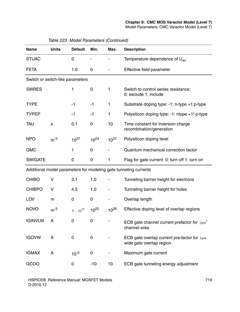
HSPICE® Reference Manual: MOSFET Models 719D-2010.12
Chapter 9: CMC MOS Varactor Model (Level 7)Model Parameters: CMC Varactor Model (Level 7)
STUAC 0 - - Temperature dependence of Uac
FETA 1.0 0 - Effective field parameter
Switch or switch-like parameters
SWRES 1 0 1 Switch to control series resistance: 0: exclude 1: include
TYPE -1 -1 1 Substrate doping type: -1: n-type +1:p-type
TYPEP -1 -1 1 Polysilicon doping type: -1: ntype +1! p-type
TAU s 0.1 0 10 Time constant for inversion charge recombination/generation
NPO m-3 1027 1024 1027 Polysilicon doping level
QMC 1 0 - Quantum mechanical correction factor
SWIGATE 0 0 1 Flag for gate current: 0: turn off 1: turn on
Additional model parameters for modeling gate tunneling currents
CHIBO V 3.1 1.0 - Tunneling barrier height for electrons
CHIBPO V 4.5 1.0 - Tunneling barrier height for holes
LOV m 0 0 - Overlap length
NOVO m-3 1022 1026 Effective doping level of overlap regions
IGINVLW A 0 0 - ECB gate channel current prefactor for channel area
IGOVW A 0 0 - ECB gate overlap current pre-factor for wide gate overlap region
IGMAX A 10-5 0 - Maximum gate current
GCOO 0 -10 10 ECB gate tunneling energy adjustment
Table 223 Model Parameters (Continued)
Name Units Default Min. Max. Description
5 1025⋅
1μm2
1μm

720 HSPICE® Reference Manual: MOSFET ModelsD-2010.12
Chapter 9: CMC MOS Varactor Model (Level 7)Model Parameters: CMC Varactor Model (Level 7)
GC2O 0.375 0 0 ECB gate current slope factor
GC3O 0.063 -10 10 ECB gate current curvature factor
IGCHVLW A 0 0 - HVB gate channel current prefactor for channel area
IGOVHVW A 0 0 - HVB gate overlap current prefactor for wide gate overlap region
GCOHVO 0 -10 10 HVB gate tunneling energy adjustment
GC2HVO 0.375 0 0 HVB gate current slope factor
GC3HVO 0.063 -10 10 HVB gate current curvature factor
IGCEVLW A 0 0 - EVB gate channel current prefactor for channel area
IGOVEVW A 0 0 - EVB gate overlap current pre-factor for wide gate overlap region
GCOEVO 0 -10 10 EVB gate tunneling energy adjustment
GC2EVO 0.375 0 0 EVB gate current slope factor
GC3EVO 0.063 -10 10 EVB gate current curvature factor
1. In PSP, VFBO corresponds to NMOS and is negative of the actual value for PMOS. For varactor, you specify the actual value.
Table 223 Model Parameters (Continued)
Name Units Default Min. Max. Description
1μm2
1μm
1μm2
1μm

HSPICE® Reference Manual: MOSFET Models 721D-2010.12
10
10MOSFET Noise Models
This chapter discusses use of available MOSFET noise model parameters.
HSPICE ships hundreds of examples for your use; see Listing of Demonstration Input Files for paths to demo files.
These topics are presented in the following sections:■ Noise Model Parameters■ MOSFET Model Noise Equations
Noise Model Parameters
This section describes noise model parameters.
Table 224 Noise Parameters
Name (Alias) Units Default Description
AF 1.0 Flicker noise exponent.
KF 0.0 Flicker noise coefficient. Reasonable values for KF
are in the range 1e-19 to 1e-25 V2F.
NLEV 2.0 Noise equation selector. Values are 1, 2, or 3.
RD V2/Hz Output thermal noise due to drain resistor.
RS V2/Hz Output thermal noise due to source resistor.

722 HSPICE® Reference Manual: MOSFET ModelsD-2010.12
Chapter 10: MOSFET Noise ModelsNoise Model Parameters
For different MOS models, the total noise equation maybe different; it always equals the sum of the noise types listed. RD, RS, ID, FN are the basic noise types (all MOSFET models contain these).
RX Transfers the function of thermal noise to the output. This is not noise, but is a transfer coefficient, which reflects the contribution of thermal noise to the output. For example:V(output) = I(local)*rx(from local to output)
Where V(output) is the noise voltage at the output port, I(local) is the local noise current in the specific noise element.
It is clear that rx should have an unit of impedance, therefore we call it transimpedance. By summarizing all the contributions (power) from each independent noisy element, we can get the total noise contribution(power) at the output port.
ID V2/Hz Output channel thermal noise: ID = RX2Þ (channel
thermal noise)2.
FN V2/Hz Output flicker noise: FN = RX2Þ (flicker noise)2.
IFEX Noise due to floating body
LGS Shot noise due to Igs
LGD Shot noise due to Igd
LGF Shot noise due to Igf
TOT V2/Hz Total output noise: TOT = RD + RS + ID + FN + IFEX + RG + IGS + IGD + IGF.
Table 224 Noise Parameters
Name (Alias) Units Default Description

HSPICE® Reference Manual: MOSFET Models 723D-2010.12
Chapter 10: MOSFET Noise ModelsMOSFET Model Noise Equations
MOSFET Model Noise Equations
The MOSFET model noise equations have a selector parameter, NLEV, that selects either the original SPICE flicker noise or an equation proposed by Gray and Meyer.
You can model thermal noise generation in the drain and source resistors as two sources, inrd and inrs (units amp/(Hz)1/2) as shown in Example 35 on page 723.
Figure 35 Equivalent Circuit, MOSFET AC Noise Analysis
The following equations calculate the values of these sources:
,
You can model the channel thermal noise and the flicker noise as the ind current source, which the following equation defines:
Substrate
gbdcbscbdgbd
gbd
inrdind
Drainrd
gmbs-vbs
gds
gm-vgs
- vds +
inrs
cgb
Source
Gate
cgs cgdrs
inrs4ktrs--------⎝ ⎠
⎛ ⎞ 1 2/= inrd
4ktrd--------⎝ ⎠
⎛ ⎞ 1 2/=

724 HSPICE® Reference Manual: MOSFET ModelsD-2010.12
Chapter 10: MOSFET Noise ModelsMOSFET Model Noise Equations
If the NLEV model parameter is less than 3, then:
The preceding formula, used in both saturation and linear regions, can lead to wrong results in the linear region. For example, at VDS=0, channel thermal noise becomes zero because gm=0. This calculation is physically impossible. If you set the NLEV model parameter to 3, simulation uses a different equation, which is valid in both linear and saturation regions. (See Operation and Modeling of the MOS Transistor by Yanis P. Tsivids, published by McGraw-Hill, 1987, p. 340.)
For NLEV=3
The following equations calculate the a value used in the preceding equation:
Use the AF and KF parameters in the small-signal AC noise analysis to determine the equivalent flicker noise current generator, which connects the drain to the source.
NLEV=0 (SPICE):
For NLEV=1
Leff2 in the above equation is replaced by Weff ⋅ Leff.
For NLEV=2, 3
ind2
channel thermal noise( )2flicker noise( )2
+=
channel thermal noise8kT gm⋅
3------------------------⎝ ⎠
⎛ ⎞ 1 2/=
channel thermal noise8kt3
-------- β vgs vth–( ) 1 a a2
+ +1 a+
------------------------ GDSNOI⋅ ⋅ ⋅ ⋅⎝ ⎠⎛ ⎞
1 2⁄=
a 1vds
vdsat--------------–= Linear region
a 0= Saturation region
flicker noiseKF IdsAF⋅
COX Leff2 f⋅ ⋅-----------------------------------------⎝ ⎠
⎛ ⎞ 1 2/=
flicker noiseKF gm2⋅
COX Weff Leff fAF⋅ ⋅ ⋅----------------------------------------------------------------⎝ ⎠
⎛ ⎞ 1 2/=

HSPICE® Reference Manual: MOSFET Models 725D-2010.12
A
AFinding Device Libraries
Describes how to use the HSPICE automatic model selector to find the proper model for each transistor size.
HSPICE ships hundreds of examples for your use; see Listing of Demonstration Input Files for paths to demo files.
The HSPICE Automatic Model Selector
For libraries with multiple models of a specific element, you can use an automatic model selector in HSPICE to automatically find the proper model for each transistor size.
The automatic model selector uses the following criteria:
If you do not specify XLREF, simulation sets it to XL. If you do not specify XWREF, simulation sets it to XW.
The model selector syntax is based on a common model root name, with a unique extension for each model.
The following is an example of HSPICE syntax for MOSFET models:
M1 drain gate source bulk NJ W=2u L=1u.MODEL NJ4 NJF WMIN=1.5u WMAX=3u LMIN=.8u LMAX=2u.MODEL NJ5 NJF WMIN=1.5u WMAX=3u LMIN=2u LMAX=6u
Figure 36 on page 726 illustrates the MOSFET model selection method.
LMIN XLREF+ L XL+ LMAX XLREF+<≤
WMIN XWREF+ W XW+ WMAX XWREF+<≤

726 HSPICE® Reference Manual: MOSFET ModelsD-2010.12
Appendix A: Finding Device LibrariesThe HSPICE Automatic Model Selector
This example illustrates several pch.x models, with varying drawn channel lengths and widths, in the model library. The model root name is “pch”, and the extensions are 1, 2, ..., 6. The NJ4 instance of the NJ Element (W=2 μ, L=1 μ) requires a model for which 1.5 μ ≤ channel width ≤ 3 μ, and 0.8 μ ≤ channel length ≤ 2 μ.
The automatic model selector chooses the pch.4 model because that model satisfies these requirements. Similarly, the NJ5 transistor requires a model with 1.5 μ ≤ channel width ≤ 3 μ, and 2 μ ≤ channel length ≤ 6 μ. The pch.5 model satisfies these requirements. If a device size is out of range for all models, the automatic model selector issues an error message.
Figure 36 Automatic Model Selector Method
If the automatic model selector cannot find a model within a subcircuit, the automatic model selector searches the top level. If the automatic model selector fails to find a model, simulation terminates.
The following combination of conditions causes the automatic model selector to fail and terminates the simulation:
Drawn
Channel
Width
Drawn Channel Length
lmax=2 mlmin=0.8 m
wmin=1.5 m
wmax=3 mx x x
x x x2 m
8 m0
1 m
1 m
3 m
4 m
pch.1
pch.4
pch.2
pch.5
pch.3
pch.6
2 m 6 m
4 m

HSPICE® Reference Manual: MOSFET Models 727D-2010.12
Appendix A: Finding Device LibrariesThe HSPICE Automatic Model Selector
■ The element statement uses a model name that contains a period (.).■ The model library was not designed for use with the automatic model
selector.■ The simulation input includes either a multisweep specification or a .TEMP
temperature analysis statement.
The following example illustrates how a period in a model name can cause problems in automatic model selection.
Example 1M1 d g s b N.CHN W=10u L=5u * Element statement.MODEL N.CHN LMIN=1u LMAX=4u WMIN=2u WMAX=100u* .MODEL statement
Example 2.TEMP 25.M1 d g s b N.CHN W=10u L=5u * Element statement.MODEL N.CHN LMIN=1u LMAX=4u WMIN=2u WMAX=100u* .MODEL statement
Because Example 1 does not specify multisweep or temperature analysis, simulation does not invoke the model selector feature, so simulation uses the N.CHN model with no problems.
In Example 2, however, the .TEMP statement invokes the model selector feature. The model selector tries to find a model named “N.nnn” that fits within the length and width ranges specified in the element statement.
Because the length in the element statement (5 μm) is not within the 1 to 4 μm range specified in the .MODEL statement, the model selector cannot find a model that matches the element statement, and simulation issues a “device ‘N’ not found” error message.

728 HSPICE® Reference Manual: MOSFET ModelsD-2010.12
Appendix A: Finding Device LibrariesThe HSPICE Automatic Model Selector

HSPICE® Reference Manual: MOSFET Models 729D-2010.12
B
BTechnology Summary for HSPICE MOSFETModels
Describes the technology used in all HSPICE MOSFET models.
These topics are covered in the following sections:■ Nonplanar and Planar Technologies■ Field Effect Transistors■ MOSFET Equivalent Circuits■ MOSFET Diode Models■ Common Threshold Voltage Equations■ MOSFET Impact Ionization■ MOS Gate Capacitance Models■ Noise Models■ Temperature Parameters and Equations
Nonplanar and Planar Technologies
Two MOSFET fabrication technologies have dominated integrated circuit design: nonplanar and planar technologies.
Nonplanar TechnologyNonplanar technology uses metal gates. The simplicity of the process generally provides acceptable yields.

730 HSPICE® Reference Manual: MOSFET ModelsD-2010.12
Appendix B: Technology Summary for HSPICE MOSFET ModelsField Effect Transistors
The primary problem with metal gates is metal breakage across the field oxide steps. Field oxide grows when oxidizing the silicon surface. When the surface is cut, it forms a sharp edge. Because metal is affixed to these edges to contact the diffusion or make a gate, thicker metal must be applied to compensate for the sharp edges. This metal tends to gather in the cuts, making etching difficult.
The inability to accurately control the metal width necessitates very conservative design rules and results in low transistor gains.
Planar Technology:In planar technology, the oxide edges are smooth with a minimal variance in metal thickness. Shifting to nitride is accomplished using polysilicon gates.
Adding a chemical reactor to the MOS fabrication process enables depositing silicon nitride, silicon oxide, and polysilicon. The ion implanter is the key element in this processing by using implanters with beam currents greater than 10 milliamperes.
Because implanters define threshold voltages, diffusions, and field thresholds, processes require a minimum number of high temperature oven steps. This enables low temperature processing and maskless pattern generation. The new wave processes are more similar to the older nonplanar metal gate technologies.
Field Effect Transistors
The metal gate MOSFET is nonisoplanar as shown in Figure 37 and Figure 38 on page 731.
Figure 37 Field Effect Transistor
C FGateSource Drain
Source-drain put into the field oxide
Metal used to form the MOS gate, as
Thin oxide cut
Source drain to metal contact
well as contacting the source and drain

HSPICE® Reference Manual: MOSFET Models 731D-2010.12
Appendix B: Technology Summary for HSPICE MOSFET ModelsField Effect Transistors
Looking at the actual geometry, from source-to-drain, Figure 38 shows a perspective of the nonisoplanar MOSFET.
Figure 38 Field Effect Transistor Geometry
To visualize the construction of a silicon gate MOSFET, observe how a source or drain to field cuts (Figure 39.) Cut A-B shows a drain contact (Figure 40).
Contact
FieldMetal
DrainSource
Gate Oxide
Gate Center
Oxide
6 7 8 9 10 13 11 12
1 2 3 4 5
Drawn metal gate channel lengthDrawn oxide cutEffective channel lengthEtched channel lengthLateral diffusionDrawn diffusion edgeActual diffusion edge
1 - 42 - 37 - 86 - 98 - 9511
E F

732 HSPICE® Reference Manual: MOSFET ModelsD-2010.12
Appendix B: Technology Summary for HSPICE MOSFET ModelsField Effect Transistors
Figure 39 Isoplanar Silicon Gate Transistor
Figure 40 Isoplanar MOSFET Construction, Part A
E A
DC
F B
Source Gate Drain
Drawn pattern for nitride definition and subsequentsource-drain diffusion formationPolysilicon definition where the poly crosses thesource-drain diffusion on MOS gate is formedSource-drain to metal contact
A BDiffusion
ContactCenter
IntermediateOxide
FieldOxide
2
3 4 5 6 7 8
Diffusion drawn dimension for nitrideNitride layer width after etchPeriphery of the diode
1 - 24 - 73 - 1
Field Implant

HSPICE® Reference Manual: MOSFET Models 733D-2010.12
Appendix B: Technology Summary for HSPICE MOSFET ModelsField Effect Transistors
CD represents the cut from the source to the drain (Figure 41 on page 733), and includes the contacts.
Figure 41 Isoplanar MOSFET Construction, Part B
The planar process produces parasitic capacitances at the poly to field edges of the device. The cut along the width of the device demonstrates the importance of these parasitics (Figure 42 on page 734).
The encroachment of the field implant into the channel narrows the channel width, and increases the gate to bulk parasitic capacitance.
C DDrain
ContactCenter
IntermediateOxide
FieldOxide
69 0 1 52
GateGate Oxide
7 3 4 810
Field Implant
Source
Drawn channel length LActual poly width after etching L + XL where XL<0Effective channel length after diffusion L + XL - LDLateral diffusion LDDiffusion periphery for diode calculationsGate edge to center contact for ACM=1 and ACM=2 calculations
7 - 82 - 53 - 44 - 59 - 105 - 6

734 HSPICE® Reference Manual: MOSFET ModelsD-2010.12
Appendix B: Technology Summary for HSPICE MOSFET ModelsMOSFET Equivalent Circuits
Figure 42 Isoplanar MOSFET, Width Cut
MOSFET Equivalent Circuits
The following sections describe MOSFET equation variables, current convention, and equivalent circuits.
Equation VariablesThis section lists the equation variables and constants.
Table 225 Equation variables and Constants
Variable/Quantity Definition
cbd Bulk-to-drain capacitance
Field Implant
E F
5 6
2
3 4
1
SubstrateGate Oxide
Gate
IntermediateOxide
ContactHole
FieldOxide
Polysilicon
Drawn width of the gate W1 - 23 - 44 - 53 - 6
Depleted or accumulated channel (parameter WD)Effective channel width W+ XW -2 WDPhysical channel width W + XW

HSPICE® Reference Manual: MOSFET Models 735D-2010.12
Appendix B: Technology Summary for HSPICE MOSFET ModelsMOSFET Equivalent Circuits
cbs Bulk-to-source capacitance
cbg Gate-to-bulk capacitance
cgd Gate-to-drain capacitance
cgs Gate-to-source capacitance
f Frequency
gbd Bulk-to-drain dynamic conductance
gbs Bulk-to-source dynamic conductance
gds Drain-to-source dynamic conductance (controlled by vds)
gdb Drain-to-bulk impact ionization conductance
gm Drain-to-source dynamic transconductance (controlled by vgs)
gmbs Drain-to-source dynamic bulk transconductance (controlled by vsb)
ibd Bulk-to-drain DC current
ibs Bulk-to-source DC current
ids Drain-to-source DC current
idb Drain-to-bulk impact ionization current
ind Drain-to-source equivalent noise circuit
inrd Drain resistor equivalent noise circuit
inrs Source resistor equivalent noise circuit
rd Drain resistance
rs Source resistance
vsb Source-to-bulk voltage
Table 225 Equation variables and Constants
Variable/Quantity Definition

736 HSPICE® Reference Manual: MOSFET ModelsD-2010.12
Appendix B: Technology Summary for HSPICE MOSFET ModelsMOSFET Equivalent Circuits
Using MOSFET Current ConventionFigure 43 shows the assumed direction of current flow through a MOS transistor. To print the drain current, use either I(M1) or I1(M1) syntax. ■ I2 produces the gate current.■ I3 produces the source current.■ I4 produces the substrate current.
References to bulk are the same as references to the substrate.
vds Drain-to-source voltage
vgs Gate-to-source voltage
t-tnom
1.0359e-10F/m dielectric constant of silicon
k 1.38062e-23 (Boltzmann’s constant)
q 1.60212e-19 (electron charge)
t New temperature of model or element in ° K
tnom tnom = TNOM + 273.15. This variable represents the nominal temperature of parameter measurements in ° K (user input in ° C).
vt k ⋅ t/q
vt(tnom) k ⋅ tnom/q
Table 225 Equation variables and Constants
Variable/Quantity Definition
Δt
εsi

HSPICE® Reference Manual: MOSFET Models 737D-2010.12
Appendix B: Technology Summary for HSPICE MOSFET ModelsMOSFET Equivalent Circuits
Figure 43 MOSFET Current Convention, N-channel
Using MOSFET Equivalent CircuitsSimulators use three equivalent circuits to analyze MOSFETs: ■ DC■ Transient■ AC and noise-equivalent circuits
The components of these circuits form the basis for all element and model equations. The equivalent circuit for DC sweep is the same as the one used for transient analysis, but excludes capacitances. Figure 44 through Figure 46 display the MOSFET equivalent circuits.
The fundamental component in the equivalent circuit is the DC drain-to-source current (ids). Noise and AC analyses do not use the actual ids current. Instead, the model uses the partial derivatives of ids with respect to the vgs, vds, and vbs terminal voltages.
The names for these partial derivatives are as follows.
Transconductance:
Conductance:
Bulk Transconductance:
nd (drain node)11 (MI)
ns (source node)13 (MI)
ng (gate node)12 (MI)
nb (substrate node)14 (MI)
gmids( )∂vgs( )∂
----------------=
gdsids( )∂vds( )∂
----------------=
gmbsids( )∂vbs( )∂
----------------=

738 HSPICE® Reference Manual: MOSFET ModelsD-2010.12
Appendix B: Technology Summary for HSPICE MOSFET ModelsMOSFET Equivalent Circuits
The ids equation describes the basic DC effects of the MOSFET. Simulation considers the effects of gate capacitance, and of source and drain diodes, separately from the DC ids equations. Simulation also evaluates the impact ionization equations separately from the DC ids equation, even though the ionization effects are added to ids.
Figure 44 Equivalent Circuit, MOSFET Transient Analysis
Substrate
idbcbscbd
-
ibs
Drainrd- vds +cgb
Gate
cgs cgd
Source rs
ibdids
vbs+
-vbd+
+vgs
-
+vgd
-

HSPICE® Reference Manual: MOSFET Models 739D-2010.12
Appendix B: Technology Summary for HSPICE MOSFET ModelsMOSFET Equivalent Circuits
Figure 45 Equivalent Circuit, MOSFET AC Analysis
Substrate
gbdcbscbdgbd
gbd
Drainrd
gmbs vbsgds
gm vgs
- vds +cgb
Source
Gate
cgs cgdrs
*
*

740 HSPICE® Reference Manual: MOSFET ModelsD-2010.12
Appendix B: Technology Summary for HSPICE MOSFET ModelsMOSFET Equivalent Circuits
Figure 46 Equivalent Circuit, MOSFET AC Noise Analysis
Table 226 MOSFET DC Operating Point Output
Quantities Definitions
id drain current
ibs B-S bulk-to-source current
ibd B-D bulk-to-drain current
vgs G-S gate-source voltage
vds D-S drain-source voltage
vbs B-S bulk-source voltage
vth threshold voltage
vdsat saturation voltage
Substrate
gbdcbscbdgbd
gbd
inrdind
Drainrd
gmbs-vbs
gds
gm-vgs
- vds +
inrs
cgb
Source
Gate
cgs cgdrs

HSPICE® Reference Manual: MOSFET Models 741D-2010.12
Appendix B: Technology Summary for HSPICE MOSFET ModelsMOSFET Diode Models
MOSFET Diode Models
See Chapter 8, MOSFET Diode Modelsfor full discussion of available MOSFET diode models and parameters.
beta beta value
gam eff gamma effective
gm DC gate transconductance
gds D-S drain-source conductance
gmb B-S bulk-source conductance
cdtot total drain capacitance
cgtot total gate capacitance
cstot total source capacitance
cbtot total bulk capacitance (total floating body capacitance for SOI MOSFET)
cgs total gat- to-source capacitance
cgd total gat- to-drain capacitance
Table 226 MOSFET DC Operating Point Output
Quantities Definitions

742 HSPICE® Reference Manual: MOSFET ModelsD-2010.12
Appendix B: Technology Summary for HSPICE MOSFET ModelsCommon Threshold Voltage Equations
Common Threshold Voltage Equations
Common Threshold Voltage ParametersThe parameters described in this section apply to all MOSFET models except Levels 5 and 13.
Table 227 MOSFET Common Threshold Voltage Parameters
Name (Alias) Units Default Description
DELVTO V 0.0 Zero-bias threshold voltage shift.
GAMMA V1/2 0.527625 Body effect factor. If you do not set GAMMA, simulation calculates it from NSUB.
NGATE 1/cm3 - Polysilicon gate doping, used for analytical models only. Undoped polysilicon is represented by a small value. If NGATE ≤ 0.0, it is set to 1e+18.
NSS 1/cm2 1.0 Surface state density.
NSUB (DNB, NB) 1/cm3 1e15 Substrate doping.
PHI V 0.576036 Surface potential. NSUB default=1e15.
TPG (TPS) - 1.0 Type of gate material for analytical models.LEVEL 4 TPG default=0. The TPG value can be:■ TPG = 0 al-gate.■ TPG = 1 same as source-drain
diffusion.■ TPG = -1 gate type opposite to
source-drain diffusion.
VTO (VT) V - Zero-bias threshold voltage.

HSPICE® Reference Manual: MOSFET Models 743D-2010.12
Appendix B: Technology Summary for HSPICE MOSFET ModelsCommon Threshold Voltage Equations
Calculating PHI, GAMMA, and VTOUse the PHI, GAMMA, and VTO model parameters to calculate threshold voltages. If you do not specify these parameters, simulation calculates them as follows, except for the LEVEL 5 model.
If you do not specify PHI, then:
If you do not specify GAMMA, then:
The following equations determines the energy gap (eg) and intrinsic carrier concentration used in the above equations:
In the preceding equation, .
If you do not specify VTO, then for Al-Gate (TPG=0), the following equation
determines the ms work function:
In the preceding equation, type is +1 for n-channel or -1 for p-channel.
For Poly-Gate (TPG=±1), the following equations determine the work function.
If you do not specify the NGATE model parameter, then:
If you specify NGATE, then:
If you do not specify the VTO model parameter, then the following equation
determines the VTO voltage:
In the preceding equation, .
PHI 2 vt lnNSUB
ni----------------⎝ ⎠
⎛ ⎞⋅ ⋅=
GAMMA2 q ε si NSUB⋅ ⋅ ⋅( )1 2⁄
COX------------------------------------------------------------------=
eg 1.16 - 7.02e-4tnom2
tnom 1108+-------------------------------⋅=
ni 1.45e+10tnom300
-------------⎝ ⎠⎛ ⎞ 3 2⁄
eq eg⋅2 k⋅
---------------- 1300--------- 1
tnom-------------–⎝ ⎠
⎛ ⎞⋅1/cm
3( )⋅ ⋅=
tnom TNOM 273.15+=
Φ Φms -eg2------ - type
PHI2
----------⋅ 0.05–=
Φms type - TPGeg2
------⋅ PHI2
----------–⎝ ⎠⎛ ⎞⋅=
Φms type - TPG vt lnNGATE
ni--------------------⎝ ⎠
⎛ ⎞⋅ ⋅ PHI2
----------–⋅=
VTO vfb type GAMMA PHI1 2⁄⋅ PHI+( )⋅+=
vfb Φmsq NSS⋅
COX---------------------– DELVTO+=

744 HSPICE® Reference Manual: MOSFET ModelsD-2010.12
Appendix B: Technology Summary for HSPICE MOSFET ModelsMOSFET Impact Ionization
If you specify VTO, then: .
MOSFET Impact Ionization
Impact ionization current is available for all MOSFET levels. ALPHA, VCR, and IIRAT are the controlling parameters. IIRAT sets the fraction of the impact ionization current sent to the source.
Ids = Ids_normal + IIRAT⋅ I_impact Idb = Idb_diode + (1-IIRAT)⋅ I_impact
IIRAT defaults to zero, which sends all impact ionization current to bulk. Leave IIRAT at its default value unless data is available for both drain and bulk current.
Calculating the Impact Ionization EquationsThe following equations calculates the I_impact current due to the impact
ionization effect:
Table 228 Impact Ionization Model Parameters
Name (Alias) Units Default Description
ALPHA 1/V 0.0 Impact ionization current coefficient
LALPHA μm/V 0.0 ALPHA length sensitivity
WALPHA μm/V 0.0 ALPHA width sensitivity
VCR V 0.0 Critical voltage
LVCR μm ⋅ V 0.0 VCR length sensitivity
WVCR μm ⋅ V 0.0 VCR width sensitivity
IIRAT 0.0 Portion of impact ionization current sent to the source
VTO VTO DELVTO+=
I_impact Ids ALPHAeff vds vdsat–( ) eVCReff–
vds vdsat–----------------------------
⋅ ⋅ ⋅=

HSPICE® Reference Manual: MOSFET Models 745D-2010.12
Appendix B: Technology Summary for HSPICE MOSFET ModelsMOSFET Impact Ionization
The following equations calculate values used in the preceding equation:
The following equations calculate the LREFeff and WREFeff values used in the preceding equations:
Calculating Effective Output ConductanceYou can use the element template to directly output gds. For example:
.PRINT I(M1) gds=LX8(M1)
If you use impact ionization current, gds is the derivative of Ids only, rather than the total drain current, which is Ids+Idb.
The complete drain output conductance is:
For example, to print the drain output resistance of the M1 device:
.PRINT rout=PAR(’1.0/(LX8(M1)+LX10(M1))’)
ALPHAeff ALPHA LALPHA 1e-61
Leff---------- 1
LREFeff----------------------–⎝ ⎠
⎛ ⎞⋅ ⋅+=
WALPHA 1e-61
Weff------------ 1
WREFeff------------------------–⎝ ⎠
⎛ ⎞⋅ ⋅
VCReff VCR LVCR 1e-61
Leff---------- 1
LREFeff----------------------–⎝ ⎠
⎛ ⎞⋅ ⋅+=
WVCR 1e-61
Weff------------ 1
WREFeff------------------------–⎝ ⎠
⎛ ⎞⋅ ⋅
LREFeff LREF XLREF 2 LD⋅–+=
WREFeff WREF XWREF 2 WD⋅–+=
gdd
∂Id
∂Vd---------
∂Ids
∂Vds-----------
∂Idb
∂Vdb-----------+
∂Ids
∂Vds-----------
∂Ibd
∂Vbd-----------+ gds gbd+= = = =
Gdd LX8 LX10+=

746 HSPICE® Reference Manual: MOSFET ModelsD-2010.12
Appendix B: Technology Summary for HSPICE MOSFET ModelsMOSFET Impact Ionization
Figure 47 Drain, Source, and Bulk Currents for vgs=3 with IIRAT=0.5
Cascoding ExampleDrain-to-bulk impact ionization current limits the use of cascoding to increase output impedance. The following cascode example shows the effect of changing IIRAT. If IIRAT is less than 1.0, the drain-to-bulk current lowers the output impedance of the cascode stage.
Figure 48 Low-frequency AC Analysis Measuring Output Impedance
0
0
ref
in

HSPICE® Reference Manual: MOSFET Models 747D-2010.12
Appendix B: Technology Summary for HSPICE MOSFET ModelsMOS Gate Capacitance Models
Cascode CircuitExampleiirat gout_ac rout
0.0 8.86E-6 113 K0.5 4.30E-6 233 K1.0 5.31E-8 18.8 Meg
This example is based on demonstration netlist cascode.sp, which is available in directory $<installdir>/demo/hspice/mos:
$ cascode test.option post.param pvds=5.0 pvref=1.4 pvin=3.0vdd dd 0 pvds ac 1$ current monitor vdvd dd d 0vin in 0 pvinvref ref 0 pvrefx1 d in ref cascode.macro cascode out in refm1 out in 1 0 n L=1u W=10umref 1 ref 0 0 n L=1u W=10u.eom.param xiirat=0.ac dec 2 100k 1x sweep xiirat poi 3 0, 0.5, 1.0.print ir(vd).measure gout_ac avg ir(vd).model n nmos level=3+ tox=200 vto=0.8 gamma=0.7 uo=600 kappa=0.05+ alpha=1 vcr=15 iirat=xiirat.end
MOS Gate Capacitance Models
See Chapter 7, MOSFET Capacitance Models for full discussion of these models and their parameters.

748 HSPICE® Reference Manual: MOSFET ModelsD-2010.12
Appendix B: Technology Summary for HSPICE MOSFET ModelsNoise Models
Noise Models
See MOSFET Noise Models for discussion of parameters and noise model equations.
Temperature Parameters and Equations
Temperature ParametersThe following temperature parameters apply to all MOSFET model levels and the associated bulk-to-drain and bulk-to-source MOSFET diode within the MOSFET model. The TLEV and TLEVC parameters select the temperature equations used to calculate the temperature effects on the model parameters.
Table 229 Temperature Effects Parameters
Name (Alias) Units Default Description
BEX -1.5 Low field mobility, UO, temperature exponent.
CTA 1/° K 0.0 Junction capacitance (CJ) temperature coefficient. If TLEVC=1, CTA overrides the default temperature compensation.
CTP 1/° K 0.0 Junction sidewall capacitance (CJSW) temperature coefficient. If TLEVC=1, CTP overrides the default temperature compensation.
EG eV Energy gap for pn junction diodefor TLEV=0 or 1, default=1.11;for TLEV=2, default=1.161.17 – silicon0.69 – Schottky barrier diode0.67 – germanium1.52 – gallium arsenide
F1EX 0 Bulk junction bottom grading coefficient

HSPICE® Reference Manual: MOSFET Models 749D-2010.12
Appendix B: Technology Summary for HSPICE MOSFET ModelsTemperature Parameters and Equations
GAP1 eV/° K 7.02e-4 First bandgap correction factor (from Sze, alpha term).7.02e-4 – silicon4.73e-4 – silicon4.56e-4 – germanium5.41e-4 – gallium arsenide
GAP2 ° K 1108 Second bandgap correction factor (from Sze, beta term).1108 – silicon636 – silicon 210 – germanium 204 – gallium arsenide
LAMEX 1/° K 0 LAMBDA temperature coefficient.
N 1.0 Emission coefficient.
MJ 0.5 Bulk junction bottom grading coefficient.
MJSW 0.33 Bulk junction sidewall grading coefficient.
PTA V/° K 0.0 Junction potential (PB) temperature coefficient. If you set TLEVC to 1 or 2, PTA overrides the default temperature compensation.
PTC V/° K 0.0 Fermi potential (PHI) temperature coefficient. If you set TLEVC to 1 or 2, PTC overrides the default temperature compensation.
PTP V/° K 0.0 Junction potential (PHP) temperature coefficient. If TLEVC=1 or 2, PTP overrides the default temperature compensation.
TCV V/° K 0.0 Threshold voltage temperature coefficient. Typical values are +1mV for n-channel and -1mV for p-channel.
Table 229 Temperature Effects Parameters
Name (Alias) Units Default Description

750 HSPICE® Reference Manual: MOSFET ModelsD-2010.12
Appendix B: Technology Summary for HSPICE MOSFET ModelsTemperature Parameters and Equations
MOS Temperature Coefficient Sensitivity ParametersModel levels 13 (BSIM1), 39 (BSIM2), and 28 (METAMOS) include length and width sensitivity parameters as shown in Table 230. Use these parameters with the Automatic Model Selector to enable more accurate modeling for various device sizes. The default value of each sensitivity parameter is zero to ensure backward compatibility.
TLEV 0.0 Temperature equation level selector. Set TLEV=1 for ASPEC style. Default is SPICE style. If you invoke the ASPEC option, the program sets TLEV for ASPEC.
TLEVC 0.0 Temperature equation level selector for junction capacitances and potentials. Interacts with TLEV. Set TLEVC=1 for ASPEC style. Default is SPICE style. If you invoke the ASPEC option, the program sets TLEVC for ASPEC.
TRD 1/° K 0.0 Temperature coefficient for drain resistor.
TRS 1/° K 0.0 Temperature coefficient for source resistor.
XTI 0.0 Saturation current temperature exponent. Use XTI=3 for silicon diffused junction. Set XTI=2 for Schottky barrier diode.
Table 230 MOS Temperature Coefficient Sensitivity Parameters
Parameter Description
Sensitivity Parameters
Length Width Product
BEX Low field mobility, UO, temperature exponent
LBEX WBEX PBEX
FEX Velocity saturation temperature exponent
LFEX WFEX PFEX
TCV Threshold voltage temperature coefficient
LTCV WTCV PTCV
Table 229 Temperature Effects Parameters
Name (Alias) Units Default Description

HSPICE® Reference Manual: MOSFET Models 751D-2010.12
Appendix B: Technology Summary for HSPICE MOSFET ModelsTemperature Parameters and Equations
Temperature EquationsThis section describes how to use temperature equations.
Energy Gap Temperature EquationsThese equations set the energy gap for temperature compensation:
For TLEV = 0 or 1
For TLEV = 2
Saturation Current Temperature Equations
,
The following equation calculates the facln value used in the preceding equations:
TRS Temperature coefficient for source resistor
LTRS WTRS PTRS
TRD Temperature coefficient for drain resistor
LTRD WTRD PTRD
Table 230 MOS Temperature Coefficient Sensitivity Parameters
Parameter Description
Sensitivity Parameters
Length Width Product
egnom 1.16 – 7.02e–4tnom2
tnom 1108.0+-----------------------------------⋅=
eg t( ) 1.16 – 7.02e–4t2
t 1108.0+------------------------⋅=
egnom EG GAP1–tnom2
tnom GAP2+-----------------------------------⋅=
eg t( ) EG GAP1–t2
t GAP2+-----------------------⋅=
isbd t( ) isbd tnom( ) e facln N/⋅= isbs t( ) isbs tnom( ) e facln N/⋅=

752 HSPICE® Reference Manual: MOSFET ModelsD-2010.12
Appendix B: Technology Summary for HSPICE MOSFET ModelsTemperature Parameters and Equations
MOSFET Diode Models on page 741 defines the isbd and isbs values.
MOS Diode Capacitance Temperature EquationsTLEVC selects the temperature equation level for MOS diode capacitance.
For TLEVC=0
For TLEVC=1
,
,
,
For TLEVC=2
,
,
,
faclnegnom
vt tnom( )--------------------- eg t( )
vt t( )-----------– XTI ln
ttnom-------------⎝ ⎠
⎛ ⎞⋅+=
PB t( ) PBt
tnom-------------⎝ ⎠
⎛ ⎞⋅ vt t( ) ⇒ 3 lnt
tnom-------------⎝ ⎠
⎛ ⎞ egnomvt tnom( )--------------------- eg t( )
vt t( )-----------–+⋅–=
PHP t( ) PHPt
tnom-------------⎝ ⎠
⎛ ⎞⋅ vt t( ) ⇒ 3 lnt
tnom-------------⎝ ⎠
⎛ ⎞⋅ egnomvt tnom( )--------------------- eg t( )
vt t( )-----------–+–=
CBD t( ) CBD 1 MJ 400u ΔtPB t( )PB
-------------– 1+⋅⎝ ⎠⎛ ⎞⋅+⋅=
CBS t( ) CBS 1 MJ 400u ΔtPB t( )PB
-------------– 1+⋅⎝ ⎠⎛ ⎞⋅+⋅=
CJ t( ) CJ 1 MJ 400u ΔtPB t( )PB
-------------– 1+⋅⎝ ⎠⎛ ⎞⋅+⋅=
CJSW t( ) CJSW 1 MJSW 400u ΔtPHP t( )PHP
------------------– 1+⋅⎝ ⎠⎛ ⎞⋅+⋅=
PB t( ) PB PTA ⇒Δt–= PHP t( ) PHP PTP ⇒Δt–=
CBD t( ) CBD 1 CTA Δt⋅+( )⋅= CBS t( ) CBS 1 CTA Δt⋅+( )⋅=
CJ CJ 1 CTA Δt⋅+( )⋅= CJSW CJSW 1 CTP Δt⋅+( )⋅=
PB t( ) PB PTA ⇒Δt–= PHP t( ) PHP PTP ⇒Δt–=
CBD t( ) CBDPB
PB t( )--------------⎝ ⎠
⎛ ⎞ MJ⋅= CBS t( ) CBS
PBPB t( )--------------⎝ ⎠
⎛ ⎞ MJ⋅=
CJ t( ) CJPB
PB t( )--------------⎝ ⎠
⎛ ⎞ MJ⋅= CJSW t( ) CJSW
PHPPHP t( )-------------------⎝ ⎠
⎛ ⎞ MJSW⋅=
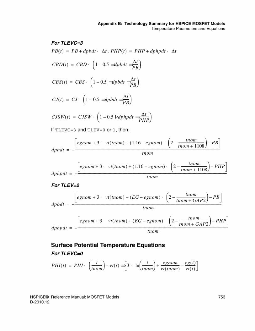
HSPICE® Reference Manual: MOSFET Models 753D-2010.12
Appendix B: Technology Summary for HSPICE MOSFET ModelsTemperature Parameters and Equations
For TLEVC=3
,
If TLEVC=3 and TLEV=0 or 1, then:
For TLEV=2
Surface Potential Temperature EquationsFor TLEVC=0
PB t( ) PB dpbdt Δt⋅+= PHP t( ) PHP dphpdt Δt⋅+=
CBD t( ) CBD 1 0.5 ⇒dpbdt ⇒ΔtPB-------–⎝ ⎠
⎛ ⎞⋅=
CBS t( ) CBS 1 0.5 ⇒dpbdt ⇒ΔtPB-------–⎝ ⎠
⎛ ⎞⋅=
CJ t( ) CJ 1 0.5 ⇒dpbdt ⇒ΔtPB-------–⎝ ⎠
⎛ ⎞⋅=
CJSW t( ) CJSW 1 0.5 Þdphpdt ⇒ ΔtPHP------------–⎝ ⎠
⎛ ⎞⋅=
dpbdt
egnom 3 vt tnom( )⋅ 1.16 egnom–( ) 2tnom
tnom 1108+-------------------------------–⎝ ⎠
⎛ ⎞⋅ PB–+ +
tnom------------------------------------------------------------------------------------------------------------------------------------------------------------------------------–=
dphpdt
egnom 3 vt tnom( )⋅ 1.16 egnom–( ) 2tnom
tnom 1108+-------------------------------–⎝ ⎠
⎛ ⎞⋅ PHP–+ +
tnom-----------------------------------------------------------------------------------------------------------------------------------------------------------------------------------–=
dpbdt
egnom 3 vt tnom( )⋅ EG egnom–( ) 2tnom
tnom GAP2+-----------------------------------–⎝ ⎠
⎛ ⎞⋅ PB–+ +
tnom--------------------------------------------------------------------------------------------------------------------------------------------------------------------------------–=
dphpdt
egnom 3 vt tnom( )⋅ EG egnom–( ) 2tnom
tnom GAP2+-----------------------------------–⎝ ⎠
⎛ ⎞⋅ PHP–+ +
tnom-------------------------------------------------------------------------------------------------------------------------------------------------------------------------------------–=
PHI t( ) PHIt
tnom-------------⎝ ⎠
⎛ ⎞⋅ vt t( ) ⇒ 3 lnt
tnom-------------⎝ ⎠
⎛ ⎞⋅ egnomvt tnom( )---------------------- eg t( )
vt t( )------------–+–=

754 HSPICE® Reference Manual: MOSFET ModelsD-2010.12
Appendix B: Technology Summary for HSPICE MOSFET ModelsTemperature Parameters and Equations
For TLEVC=1
If you do not specify the PHI parameter, simulation calculates it as:
The intrinsic carrier concentration, ni, must be temperature updated, and it is calculated from the silicon bandgap at room temperature.
For TLEVC=2
For TLEVC=3
If TLEVC=3 and TLEV=0 or 1, then:
For TLEV=2
Threshold Voltage Temperature EquationsThe threshold temperature equations are:
For TLEV=0
For TLEV=1
PHI t( ) PHI PTC ⇒Δt–=
PHI t( ) 2 vt t( ) lnNSUB
ni----------------⎝ ⎠
⎛ ⎞⋅ ⋅=
ni 145e16t
tnom-------------⎝ ⎠
⎛ ⎞ 3 2/exp EG
ttnom------------- 1–⎝ ⎠
⎛ ⎞ 12 vt t( )⋅---------------------⎝ ⎠
⎛ ⎞⋅ ⋅⋅ ⋅=
PHI t( ) PHI PTC ⇒Δt–=
PHI t( ) PHI dphidt Δt⋅+=
dphidt
egnom 3 vt tnom( )⋅ 1.16 egnom–( ) 2tnom
tnom 1108+-------------------------------–⎝ ⎠
⎛ ⎞⋅ PHI–+ +
tnom---------------------------------------------------------------------------------------------------------------------------------------------------------------------------------–=
dphidt
egnom 3 vt tnom( )⋅ EG egnom–( ) 2tnom
tnom GAP2+-----------------------------------–⎝ ⎠
⎛ ⎞⋅ PHI–+ +
tnom-----------------------------------------------------------------------------------------------------------------------------------------------------------------------------------–=
vbi t( ) vbi tnom( ) PHI t( ) PHI–2
---------------------------------- egnom eg t( )–2
------------------------------------+ +=
VTO t( ) vbi t( ) GAMMA PHI t( )( )1 2/⋅+=
VTO t( ) VTO TCV ÞΔt–=

HSPICE® Reference Manual: MOSFET Models 755D-2010.12
Appendix B: Technology Summary for HSPICE MOSFET ModelsTemperature Parameters and Equations
For TLEV=2
Mobility Temperature EquationsThe MOS mobility temperature equations are:
Channel Length Modulation Temperature EquationIf you specify the LAMEX model parameter, then the temperature modifies the LAMBDA value.
Calculating Diode Resistance Temperature EquationsThe following equations are examples of the effective drain and source resistance:
,
vbi t( ) VTO t( ) GAMMA Þ PHI t( )( )1 2/–=
VTO t( ) VTO 1GAMMA
2 PHI1 2/⋅----------------------------+⎝ ⎠
⎛ ⎞ dphidt Δt⋅ ⋅+=
vbi t( ) VTO t( ) GAMMA Þ PHI t( )( )1 2/–=
UO t( ) UOt
tnom-------------⎝ ⎠
⎛ ⎞ BEX⋅=
KP t( ) KPt
tnom-------------⎝ ⎠
⎛ ⎞ BEX⋅=
F1 t( ) F1t
tnom-------------⎝ ⎠
⎛ ⎞ F1EX⋅=
LAMBDA t( ) LAMBDA 1 LAMEX Δt⋅+( )⋅=
RD t( ) RS 1 TRD Δt⋅+( )⋅= RS t( ) RS 1 TRS Δt⋅+( )⋅=

756 HSPICE® Reference Manual: MOSFET ModelsD-2010.12
Appendix B: Technology Summary for HSPICE MOSFET ModelsTemperature Parameters and Equations

757
Index
AAC analysis, MOSFETs 739ACM
model parameter 695MOS diode 698, 701, 704, 707parameter 14, 693, 694
alternate saturation model parameters 96AMD models 9, 11AMI gate capacitance model 689analysis
MOSFETsAC 723, 739, 740transient 738
ASPECAMI model 9compatibility 9, 123, 704option 14
automatic model selectionfailure 726multisweep or .TEMP effect 727See also model selection
avalanche impact ionizationparameters, MOSFETs, LEVEL 57 526, 606
Bbasic model parameters
LEVEL 1 46LEVEL 2 52LEVEL 27 133LEVEL 39 380LEVEL 47 404LEVEL 49, 53 444LEVEL 5 52LEVEL 50 162LEVEL 57 516LEVEL 58 199LEVELs 6, 7 52
BerkeleyBSIM3-SOI model 511junction model 428NonQuasi-Static (NQS) model 428
BJT models 740
BSIM model 345equations 354LEVEL 13 10, 361VERSION parameter effects 353
BSIM2 model 380equations 384LEVEL 39 11VERSION parameter effects 390
BSIM3 modelequations 411Leff/Weff 410LEVEL 47 11SOI FD 546
BSIM3 SOI FDparameters 548template output 556
BSIM3 Version 2 MOS model 404BSIM3v3
Ig model 439WPE model 438
BSIM3v3 modelHSPICE 442MOS 419
BSIM4 Juncap2 model 478BSIM4 model
parameters 486STI/LOD 481
BSIM4.5.0 466BSIM4.6.0 509BSIM-CMG model
LEVEL 72, BSIM-CMG model 629BSIMSOIv3.2 540bulk
charge effect 9transconductance, MOSFETs 737
BYPASS option 14, 17
Ccapacitance
CAPOP model selector 12control options 665equations 710

758
IndexD
modelparameters 666, 695–696selection 655
MOSFETsAC gate 691BSIM model 357diodes 710, 752equations 670–691gate capacitance 663gate capacitance example 661gate capacitance length/width 691gate capacitance models 654gate capacitance, SPICE Meyer 670Meyer model 654, 668models 655
overlap 669parameters
Meyer 668MOSFETs
LEVEL 5 84parameters, MOSFETs, Cypress 143parameters, MOSFETs, IDS - LEVEL 5 84parameters, MOSFETs, LEVEL 38 143parameters, MOSFETs, LEVEL 49 and 53 449parameters, MOSFETs, LEVEL 57 523plotting 663
capacitor modelsgate 654list 12
capacitor, transcapacitance 656CAPOP model parameter 12, 655, 666
XPART 669XQC 669
cascoding example 746CASMOS
GEC model 10GTE model 10Rutherford model 10
CBD model parameter 695CBS model parameter 695CDB model parameter 696channel length modulation
equationsLEVEL 2 73LEVEL 3 78LEVEL 38 148LEVEL 5 93LEVEL 6 118LEVEL 8 129
parametersLEVEL 6 118LEVEL 8 126
charge conservation 682, 685circuits
nonplanar and planar technologies 729wave processes 730
CJ model parameter 696CJA model parameter 696CJGATE model parameter 696CJP model parameter 696CJSW model parameter 696CMC MOS Varactor 715CMC MOS Varactor Model
Level 7 715commands
.LIB 4conductance
MOSFETs 737, 745preventing negative output 360, 390
control optionsASPEC 14BYPASS 14capacitance 665
convergence, MOSFET diodes 694CSB model parameter 696current convention 736Cypress model 10, 141
DDallas Semiconductor model 10DC
current 710parameters
MOSFETs 517, 695DEFAD option 14DEFAS option 14DEFL option 14DEFNRD option 14DEFNRS option 14DEFPD option 15DEFW option 15depletion, MOS devices 8diffusion 351diodes
capacitance equations 710, 752MOSFETs
759
IndexE
capacitance equations 710equations 709model selector 14models 14, 693, 741resistance temperature 755
DLAT model parameter 698DNB model parameter 696drain current equation 416DW model parameter 698
EEarly voltage 68effective channel length
equationsLEVEL 1 69LEVEL 13 354LEVEL 28 376LEVEL 39 386LEVEL 49 459, 462LEVEL 5 85LEVEL 6 99LEVEL 8 126
parametersLEVEL 1 53LEVEL 3 77
effective channel widthequations
LEVEL 1 69LEVEL 13 354LEVEL 2 70LEVEL 28 376LEVEL 49 459, 462LEVEL 5 85LEVEL 6 99
parametersLEVEL 1 53LEVEL 8 126
effective channel width, MOSFETsequations
LEVEL 2 70LEVEL 3 77LEVEL 39 386
effective mobilityequations
LEVEL 28 377LEVEL 3 78LEVEL 6 113LEVEL 8 128
parameters 113
EFPS option 15element
statements 4templates 21, 659
element parametersMOSFETs 707range limits 461scaling 16
Empirical model 75equations 75example 81
.ENDL command 4energy gap temperature 751EPFL-EKV MOSFETs model 171equations
BSIM LEVEL 13 354capacitance
MOS diode 752MOSFETs 710overlap 669
diodes 709, 710Frohman-Bentchkowski 115HSPICE DL 123impact ionization 744MOSFETs
channel length modulation 755diode 709, 755impact ionization 744LEVEL 61 213LEVEL 62 222, 228mobility temperature 755model parameters 743models, BSIM2 384models, BSIM3 410, 411models, Cypress 143models, Empirical 75models, EPFL-EKV 178, 191models, HP a-Si TFT 153models, IDS - LEVEL 5 85, 90models, IDS - LEVEL 6 98, 110models, IDS - LEVEL 8 126noise 723surface potential temperature 753temperature 751threshold voltage 754voltage 742
MOSFETs, models, LEVEL 49 and 53 462MOSFETs, models, modified - BSIM LEVEL 28
376

760
IndexF
MOSFETs, models, Schichman-Hodges 68, 70noise 191, 723Normal Field 116temperature
energy gap 751MOS diode capacitance 752MOSFETs 751saturation current 751
voltage 742Wang’s 122
equations, MOSFETs, models, quasi-static 189equivalent circuit 734, 737
AC analysis 739AC noise analysis 723, 740transient analysis 738variables and constants 734
EXA model parameter 696example
capacitance 661cascoding 746gate capacitance 661.MODEL CARDS NMOS model 463MOSFETs
BSIM LEVEL 13 361Empirical 81gate capacitance 661IDS LEVEL 7 104, 107
PMOS model 464EXD model parameter 696EXJ model parameter 696EXP model parameter 696EXS model parameter 696
FFC model parameter 696field effect transistor 731
See also MOSFETs, JFETsflicker noise 723Fluke-Mosaid model 10Frohman-Bentchkowski equations 115
Ggate capacitance 688
AMI 689charge sharing coefficient 669example 661length/width 691
LEVEL 39 389, 393model (CAPOP=39) 391parameters 654, 666, 747plotting 663SPICE 670
gate direct tunneling currents 439GE-CRD Franz model 10GE-Intersil model 10geometry
MOSFETs model parameters 698scaling 16transistor field effect 731
global scaling 16GMIN option 15GMINDC option 15, 694Grove-Frohman model 9
HHDIF model parameter 698HiSIM2 model 273HiSIM241 273HP a-Si TFT model 150
equations 153topology 158
HSPICEjunction diode model 428VERSION parameter 353
HSPICE DL equation 123HVMOS (Level 66) model 580
IIDS
Cypress depletion model 11equations
LEVEL 1 68LEVEL 13 354LEVEL 2 70LEVEL 3 75LEVEL 38 143LEVEL 5 85LEVEL 6 98, 110LEVEL 8 126
LEVEL 38 Cypress model 141LEVEL 5
equations 90model 83
LEVEL 6

761
IndexJ
equations 98, 110example 104, 107
LEVEL 7 model 125LEVEL 8
equations 126model 125
Ig model, BSIM3v3 439impact ionization
BSIM2 393MOSFETs 744
equations 738, 744LEVEL 39 393
inactive devicesSee latent devices
intrinsic model parameters 193ion-implanted devices 9IS model parameter 695isoplanar
MOSFETsconstruction 732, 733width cut 734
silicon gate transistor 732ISPICE LEVEL 6 model 111
JJS model parameter 695JSW model parameter 695JUNCAP model parameters 168juncap2 junction model 478junction parameters 453
Llambda equations 99, 101LATD model parameter 698latency option 17latent devices 17Lattin-Jenkins-Grove model 9LD model parameter 698LDAC parameter 691LDIF model parameter 698Level 66 model 580Level 68 HiSIM Model 273Level 68, HiSIM2.3.1 273Level 71 (TFT) model 614Level57, BSIMSOIv3.2 540levels, MOSFETs models 8, 9
.LIB command 4nesting 5
libraries 725building 4
linear region equations 414LRD model parameter 697LRS model parameter 697
MMBYPASS option 14, 17Meyer capacitance
gate 673model 654modified 677parameters 668
MJ model parameter 696MJSW model parameter 696mobility
equations 413parameters
curve fitting 61LEVEL 2 61–64LEVEL 5 64
reduction equationsLEVEL 2 72LEVEL 38 147LEVEL 5 93
model name identification 7model names, periods in 726model parameters
ACM 14basic 46–60intrinsic limits 193MOSFETs 6, 114, 117, 119, 120
LEVEL 59 548range limit 461scaling 16
model selectionautomatic 725–727failure to find a model 726program 17, 726See also automatic model selectionsyntax 6
.MODEL statement 4BSIM models 353examples, NMOS model 463MOSFETs 6VERSION parameter 353

762
IndexM
modelsautomatic selection 17bulk charge effect 9capacitance 12depletion MOS devices 8equations
LEVEL 61 213LEVEL 62 222, 228
ion-implanted devices 9MOSFETs
BSIM 345BSIM, equations 354BSIM, LEVEL 13 example 361BSIM2 380, 384BSIM3 404BSIM3-SOI DD 556BSIM3-SOI FD 546, 548, 556BSIM4 486Cypress 141, 143Empirical 75EPFL-EKV 171, 178Frohman-Bentchkowski, equations 115HP a-Si TFT 150, 153Hspice junction 428LEVEL 55, updates 195levels 8, 9LEVELs 49 and 53, equations 462modified BSIM LEVEL 28 369, 376MOS 83Philips MOS9 162quasi-static equations 189RPI a-Si TFT 209RPI Poli-Si TFT 215Schichman-Hodges 68, 69, 70SOSFETs LEVEL 27 131UFSOI 198
MOSFETs, BSIM3, equations 411MOSFETs, BSIM3, Leff/Weff 410MOSFETs, BSIM3-SOI 511MOSFETs, BSIM3v3, MOS 419MOSFETs, BSIM3v3, NQS 428MOSFETs, IDS - LEVEL 6 and LEVEL 7 96MOSFETs, IDS - LEVEL 6 equations 98MOSFETs, IDS, LEVEL 5 83MOSFETs, IDS, LEVEL 5, equations 90MOSFETs, IDS, LEVEL 6, equations 110MOSFETs, IDS, LEVEL 6, example 104, 107MOSFETs, IDS, LEVEL 7 125MOSFETs, IDS, LEVEL 8 125, 126
MOSFETs, junction 428scaling 16silicon-on-sapphire 8simulator access 5SOSFETs 8specifying 6
modified BSIM LEVEL 28equations 376models 369
MOSmodel 83
MOS2 model 9MOS3 model 9MOSFET output templates 20MOSFETmodels
levels 9MOSFETs
7-node limit 7Berkeley 556BEX factor 366bulk transconductance 737capacitance
effective length and width 691equations 670–691Meyer model 654models 655scaling parameters 665
CAPOP 666, 670–691channel length modulation 755charge
conservation model parameters 668storage modeling 654
conductance 737current convention 736diodes
DC current equations 710DC model parameters 695effective areas 699effective drain and source resistance 700, 703,
707, 709effective saturation current 700, 709equation 709equations 710GEO element parameter 707geometry model parameters 698model parameters 695model select 693resistance, model parameters 697resistance, temperature equations 755

763
IndexM
suppressing 704temperature equations 752
effectivelength and width 691output conductance 745
energy gap temperature equations 751equation variables and constants 734equivalent circuits 737
AC analysis 739AC noise analysis 723, 740transient analysis 738
examplesNMOS model 463PMOS model 464
gatecapacitance example 661capacitance model parameters 654, 666overlap capacitance model parameters 666
impact ionization equations 738, 744isoplanar
construction 732, 733silicon gate 732width cut 734
level parameter 7LEVELs 6, 7 UPDATE selector 97Meyer capacitance model parameters 668mobility temperature equations 755model parameters
A0 549A1 549A2 549AGIDL 550AGS 550ALPHA0 550ASD 554AT 555B0 550B1 550BGIDL 550BSIM3-SOI FD 548BSIM4 486CAPMOD 548CDSC 550CDSCB 550CDSCD 550CF 554CGDL 554CGDO 554CGSL 554
CGSO 554change conservation 668CIT 550CJSWG 554CKAPPA 554CLC 554CLE 554CSDESW 554CSDMIN 554CTH0 555DELTA 550DLC 554DROUT 550DSUB 550DVT0 551DVT0W 551DVT1 551DVT1W 551DVT2 551DVT2W 551DWB 551DWC 554DWG 551ETA0 551ETAB 551gate capacitance, basic 666gate capacitance, Meyer 668gate capacitance, overlap 667impact ionization 744ISBJT 551ISDIF 551ISREC 551ISTUN 552K1 552K2 552K3 552K3B 552KB1 552KETA 552KT1 555KT2 555KTIL 555LEVEL 548Level 60 560Level 70 583LINT 552MJSWG 554MOBMOD 549

764
IndexM
NCH 549NDIO 552NFACTOR 552NGATE 549NGIDL 552NLX 552NOIMOD 549noise 721NSS 553NSUB 549NTUN 552PBSWG 554PCLM 552PDIBLC1 552PDIBLC2 552PRT 555PRWB 553PRWG 553PVAG 553RBODY 553RBSH 553RDSW 553RSH 553RTH0 555SHMOD 549SII0 550SII1 550SII2 550SIID 550TBOX 549temperature 748threshold voltage 742TNOM 555TOX 549TSI 549TT 555U0 553UA 553UA1 555UB 553UB1 555UC 553UC1 555UTE 556VBSA 553VERSION 421VOFF 553VSAT 553
VSDFB 555VSDTH 555VTH0 553WINT 553WR 553XBJT 556XDIF 556XPART 555XREC 556XTUN 556See also Chapter 20
modelsAMD 9, 11AMI-ASPEC 9ASPEC-AMI 9Berkeley
BSIM3-SOI 11Berkeley, BSIM3-SOI 511Berkeley, BSIM3-SOI DD 556Berkeley, junction 428BSIM 10, 345BSIM, equations 354BSIM, LEVEL 13 example 361BSIM2 11, 380, 384BSIM3 11, 404BSIM3, equations 411BSIM3, Leff/Weff 410BSIM3-SOI FD 546BSIM3v3, MOS 419BSIM3v3, NQS 428CASMOS 10CASMOS, model (GTE style) 10CASMOS, Rutherford 10Cypress 10, 141, 143Dallas Semiconductor 10Empirical 75EPFL-EKV 11, 171, 178Fluke-Mosaid 10Frohman-Bentchkowski, equations 115GE-CRD-Franz 10GE-Intersil 10Grove-Frohman 9HP a-Si TFT 150, 153Hspice junction 428HSPICE PC version 9IDS - Cypress depletion 11IDS - LEVEL 5 83IDS - LEVEL 5 equations 90IDS - LEVEL 6 equations 98, 110

765
IndexN
IDS - LEVEL 6 example 104, 107IDS - LEVEL 7 125IDS - LEVEL 8 125, 126Lattin-Jenkins-Grove 9LEVEL 61 circuit 213LEVEL 62 222LEVELs 49 and 53 equations 462modified BSIM LEVEL 28 369, 376MOS 83MOS2 9MOS3 9MOS9 162Motorola 11National Semiconductor 11Philips MOS9 162quasi-static, equations 189RPI Poli-Si TFT 215Schichman-Hodges 9, 68, 69, 70SGS-Thomson 11Sharp 11Siemens 10, 11Sierra 1 10Sierra 2 10Siliconix 10SOSFETs 10, 131statement 6STC-ITT 10Taylor-Huang 9TI 11University of Florida SOI 11, 198user defined 10VTI 11
models, CASMOS, GEC 10n-channel specification 6, 7noise 723
model equations 723model parameters 721, 723
p-channel specification 6RPI a-Si TFT model 209saturation current 751sensitivity factors 375SPICE compatibility 9surface potential 753temperature
coefficient model parameters 750effects parameters 748parameters 748
template input 556threshold voltage
model parameters 742temperature equations 754
transconductance 737Motorola model 11Multi-Level Gamma model, example 104, 107
NN model parameter 695narrow width effect 71National Semiconductor model 11NB model parameter 696NDS model parameter 695nested library calls 5noise
MOSFETs 721equivalent circuits 723, 740models 191
parametersBSIM3v3 452
NonQuasi-Static (NQS) model 428parameters 455
Normal Field equations 116NSUB model parameter 696
Ooperating point
capacitance printout 658Early voltage 192model internal variables 192Overdrive voltage 192saturation / non-saturation flag 193saturation voltage 192SPICE-like threshold voltage 192transconductance efficiency factor 192
.OPTION MBYPASS 17output conductance 745overlap capacitors 669
Pparameter range limit
Level 54 471Level 57 527Level 70 607Levels 49/53 459
parametersnoise 721

766
IndexQ
simulator access 5voltage 742
parasiticdiode, MOSFETs LEVEL 39 394generation 704MOSFETs LEVEL 13 366
PB model parameter 696PHA model parameter 696PHD model parameter 696Philips MOS9 model 162PHP model parameter 696PHS model parameter 696PMOS model 464PRD model parameter 697PRS model parameter 697
Qquasi-static model equations 189
RRD model parameter 697RDC model parameter 697regions charge equations 358resistance 697
MOSFETs model parameters 697RL model parameter 697RPI
a-Si TFT model 209circuit 213
Poli-Si TFT model 215, 222RS model parameter 697RSC model parameter 697RSH model parameter 697
Ssaturation
carrier velocity 121current temperature 751voltage (vdsat) 356voltage equations, MOSFETs
LEVEL 1 69LEVEL 13 356LEVEL 2 71LEVEL 28 378LEVEL 3 77
LEVEL 38 146LEVEL 47 413LEVEL 5 93LEVEL 6 103, 109LEVEL 8 127
SCALE option 15, 16scaling 16
global SCALM override 16global vs model 16MOSFETs capacitance parameters 665
SCALM 15parameter
global scaling 16overriding in a model 16scaling by model 16
Schichman-Hodges model 9, 68, 69, 70sensitivity factors 375SGS-Thomson MOS model 11Sharp model 11short-channel effect 71Siemens model 10, 11Sierra 1 model 10Sierra 2 model 10silicon gate transistor 732Siliconix model 10silicon-on-sapphire devices 8SIM2 380Simpson Integration 681simulation 68SOI model 137SOSFET model 8, 10, 131SPICE
compatibilityBSIM model 362diodes 704MOSFETs
LEVEL 39 388MOSFETs, LEVEL 13 362MOSFETs, LEVEL 3 80MOSFETs, models 9UTRA model parameter 61
Meyer gate capacitances 670stacked devices 707statements
.ENDL 4
.LIB 4nesting 5

767
IndexT
STC-ITT model 10subthreshold current equations
LEVEL 13 356LEVEL 2 74LEVEL 3 79LEVEL 38 148LEVEL 5 94LEVEL 6 112LEVEL 8 130
surface potential equations 753
TTaylor-Huang model 9temperature
compensationBSIM LEVEL 13 366
effectBSIM LEVEL 13 357LEVEL 39 392
equations 751MOSFETs
channel length modulation 755diode 752, 755equations 751mobility 755parameters 748surface potential 753threshold voltage 754
parameters 748LEVEL 13 352LEVEL 28 374LEVEL 49 461LEVEL 49 and 53 451LEVEL 57 525MOSFETs, LEVEL 13 352MOSFETs, LEVEL 28 374
temperature compensation 418example 81
TFT model 614threshold voltage
BSIM LEVEL 13 356equations 742
LEVEL 1 69LEVEL 13 356LEVEL 2 71LEVEL 28 377LEVEL 3 77LEVEL 38 145
LEVEL 47 411LEVEL 5 91LEVEL 6 99LEVEL 8 127temperature 754
parameters 742LEVEL 1 57LEVEL 2 61LEVEL 5 55
TI model 11transcapacitance 656transconductance 737transient analysis 738transistors
field effect 730isoplanar silicon gate 732process parameters
LEVEL 13 347–351LEVEL 28 369LEVEL 49 444
TT model parameter 696
UUniversal Field mobility reduction 117University of California SOI model 511University of Florida SOI model 198UPDATE parameter 367
LEVEL 13 367LEVEL 6, 7 97
Vvaractor model, Level 7 715VERSION parameter 353VNDS model parameter 695voltage 742VTI model 11
WWang’s equation 122WDAC parameter 691WDEL model parameter 698well-proximity effects 438WL option 15WMLT model parameter 698WPE model, BSIM3v3 438

768
IndexX
WRD model parameter 697WRS model parameter 697
XXJ model parameter 698
XPART CAPOP model parameter 669XQC CAPOP model parameter 669
XW model parameter 698