Embed Size (px)
Citation preview

hsabaghianb @ kashanu.ac.irhsabaghianb @ kashanu.ac.ir MicroprocessorsMicroprocessors 1-1-11
I/O devices
Peripheral devices (also called I/O devices) are pieces of equipment that exchange data with a CPU
Examples: switches, LED, CRT, printers, keyboard, keypad
Speed and characteristics of these devices are very different from that of CPU so they cannot be connected directly
Interface chips are needed to resolve this problem Main function of an interface chip is to synchronize
data transfer between CPU and I/O device Data pins of interface chip are connected to CPU data
bus and I/O port pins are connected to I/O device

hsabaghianb @ kashanu.ac.irhsabaghianb @ kashanu.ac.ir MicroprocessorsMicroprocessors 1-1-22
I/O devices
Since a CPU may have multiple I/O devices, CPU data bus may be connected to data buses of multiple interface
An address decoder is used to select one device to respond to the CPU I/O request
Different CPUs deal with I/O devices differently Some CPUs have dedicated instructions for performing
input and output operations (isolated I/O) Other CPUs use the same instruction for reading from
memory and reading from input devices, as well as writing data into memory and writing data into output devices (memory-mapped I/O)
MCS-51 (8051) is memory mapped

hsabaghianb @ kashanu.ac.irhsabaghianb @ kashanu.ac.ir MicroprocessorsMicroprocessors 1-1-33
Synchronization of CPU and interface chip
There must be a mechanism to make sure that there are valid data in the interface chip when CPU reads them
Input synchronization: two ways of doing this1. Polling method
interface chip uses a status bit to indicate if it has valid data for CPU
CPU keeps checking status bit until it is set, and then reads data from interface chip
Simple method, used when CPU has nothing else to do
2. Interrupt driven method: interface chip interrupts the CPU when it has new data. CPU executes the ISR

hsabaghianb @ kashanu.ac.irhsabaghianb @ kashanu.ac.ir MicroprocessorsMicroprocessors 1-1-44
Synchronization of CPU and interface chip
Output synchronization: two ways of doing this1. Polling method
interface chip uses a status bit to indicate that the data register is empty
CPU keeps checking status bit until it is set, and then writes data into interface chip
2. Interrupt driven method: interface chip interrupts the CPU when it data register is empty. CPU executes the ISR

hsabaghianb @ kashanu.ac.irhsabaghianb @ kashanu.ac.ir MicroprocessorsMicroprocessors 1-1-55
Synchronization of CPU and interface chip
Methods used to synchronize data transfer between interface chip and I/O devices:
1. Brute force method: interface chip returns voltage levels in its input ports to CPU and makes data written by CPU directly available on its output ports All 8051 port can perform brute force I/O
2. Strobe method: During input, the I/O device activates a strobe signal when data
are stable. Interface chip latches the data For output, interface chip places output data on output port.
when data is stable, it activates a strobe signal. I/O device latches the data
3. Handshake method: two handshake signals are needed One is asserted by interface chip and the other by I/O device
hsabaghianb @ kashanu.ac.irhsabaghianb @ kashanu.ac.ir MicroprocessorsMicroprocessors 1-1-66
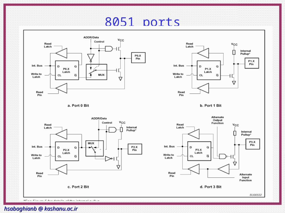
8051 ports

hsabaghianb @ kashanu.ac.irhsabaghianb @ kashanu.ac.ir MicroprocessorsMicroprocessors 1-1-77
8051 ports Ports 1, 2, and 3 have internal pullups, and
Port 0 has open drain outputs.
To be used as an input, the port bit latch must contain a 1, which turns off the output driver FET.
For Ports 1, 2, and 3, the pin is pulled high by a weak internal pullup, and can be pulled low by an external source.
Port 0 differs in that its internal pullups are not active during normal port operation (writing a 1 to the bit latch leaves both output FETs off, so the pin floats).

hsabaghianb @ kashanu.ac.irhsabaghianb @ kashanu.ac.ir MicroprocessorsMicroprocessors 1-1-88
8051 I/O Ports: Hardware Specs
P0 is open drain.Has to be pulled high by external 10K
resistors.Not needed if P0 is used for address lines
P1, P2, P3 have internal pull-upsPort fan- out (number of devices it can
drive) is limited.Use buffers (74LS244, 74LS245,etc) to
increase drive.
P1, P2, P3 can drive up to 4 LS-TTL inputs

hsabaghianb @ kashanu.ac.irhsabaghianb @ kashanu.ac.ir MicroprocessorsMicroprocessors 1-1-99
8051 - Switch On I/O Ports
Case-1: Gives a logic 0 on switch close Current is 0.5ma on switch
close
Case-2: Gives a logic 1 on switch close High current on switch close
Case-3: Can damage port if 0 is output

hsabaghianb @ kashanu.ac.irhsabaghianb @ kashanu.ac.ir MicroprocessorsMicroprocessors 1-1-1010
Simple input devices DIP switches usually have 8 switches
Use the case-1 from previous page
Sequence of instructions to read a value from DIP switches:
mov P1,#FFH
mov A,P1,

hsabaghianb @ kashanu.ac.irhsabaghianb @ kashanu.ac.ir MicroprocessorsMicroprocessors 1-1-1111
Interfacing a Keypad A 16-key keypad is built as shown in the figure below.
16 keys arranged as a 4X4 matrix.
Must “activate” each row by placing a 0 on its R output.Then the column
output is read. If there is a 0 on
one of the column bits, then the button at the column/row intersection has been pressed.
Otherwise, try next row. Repeat constantly
C 1C 2C 3C 4
R 1R 2R 3
R 4
0123
567
DEF
9AB
C
8
4

hsabaghianb @ kashanu.ac.irhsabaghianb @ kashanu.ac.ir MicroprocessorsMicroprocessors 1-1-1212
Bouncing Contacts
Push-button switches, toggle switches, and electromechanical relays all have one thing in common: contacts.
Metal contacts make and break the circuit and carry the current in switches and relays. Because they are metal, contacts have mass.
Since at least one of the contacts is movable, it has springiness.
Since contacts are designed to open and close quickly, there is little resistance (damping) to their movement

hsabaghianb @ kashanu.ac.irhsabaghianb @ kashanu.ac.ir MicroprocessorsMicroprocessors 1-1-1313
Bouncing Because the moving contacts have mass and
springiness with low damping they will be "bouncy" as they make and break.
That is, when a normally open (N.O.) pair of contacts is closed, the contacts will come together and bounce off each other several times before finally coming to rest in a closed position.
The effect is called "contact bounce" or, in a switch, "switch bounce”.

hsabaghianb @ kashanu.ac.irhsabaghianb @ kashanu.ac.ir MicroprocessorsMicroprocessors 1-1-1414
Why is it a problem?
If such a switch is used as a source to an edge-triggered input such as INT0, then the MCS-51 will think that there were several “events” and respond several times.
The bouncing of the switch may last for several milliseconds.Given that the MCS-51 operates at
microsecond speed, a short ISR may execute several times in response to the above described bounciness

hsabaghianb @ kashanu.ac.irhsabaghianb @ kashanu.ac.ir MicroprocessorsMicroprocessors 1-1-1515
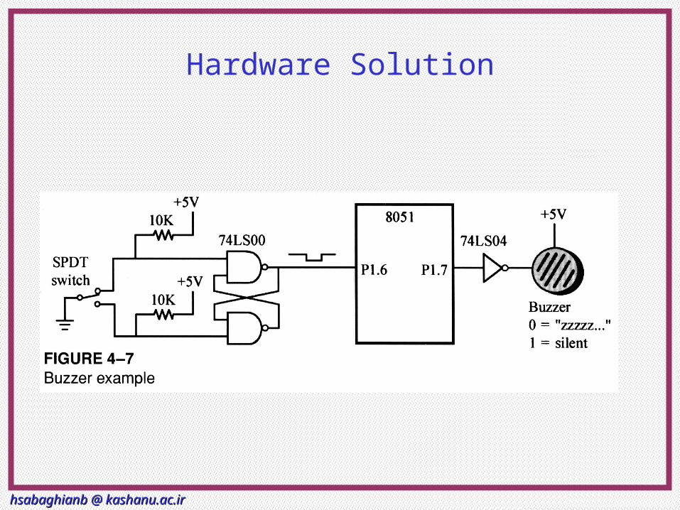
Hardware Solution
The simplest hardware solution uses an RC time constant to suppress the bounce. The time constant has to be larger than the switch bounce and is typically 0.1 seconds.
As long as capacitor voltage does not exceed a threshold value, the output signal will be continued to be recognized as a logic 1.
The buffer after the switch produces a sharp high-to-low transition.
V c c
O U T
hsabaghianb @ kashanu.ac.irhsabaghianb @ kashanu.ac.ir MicroprocessorsMicroprocessors 1-1-1616
Hardware Solution

hsabaghianb @ kashanu.ac.irhsabaghianb @ kashanu.ac.ir MicroprocessorsMicroprocessors 1-1-1717
Software Solution
It is also possible to counter the bouncing problem using software.
The easies way is the wait-and-see techniqueWhen the input drops, an “appropriate”
delay is executed (10 ms), then the value of the line is checked again to make sure the line has stopped bouncing

hsabaghianb @ kashanu.ac.irhsabaghianb @ kashanu.ac.ir MicroprocessorsMicroprocessors 1-1-1818
Interfacing a Keypad
scan: mov P1,#EFH
jnb P1.0,db_0
scan1: jnb P1.1,db_1
scan2: jnb P1.2,db_2
scan3: jnb P1.3,db_3
scan4: mov P1,#DFH
jnb P1.0,db_4
…..
…..
…..
P1.3P1.2P1.1P1.0
P1.7P1.6P1.5
P1.4
0123
567
DEF
9AB
C
8
4
8051

hsabaghianb @ kashanu.ac.irhsabaghianb @ kashanu.ac.ir MicroprocessorsMicroprocessors 1-1-1919
Interfacing a Keypaddb_0: lcall wt_10ms
jb P1.0, scan1mov A, #0ljmp get_code
db_1: lcall wt_10msjb P1.1, scan2mov A, #1ljmp get_code
…..……..
get_code: mov DPRT, #key_tabmovc A, @A+DPRTljmp scan
key_tab:db ‘0123456789ABCDEF’END

hsabaghianb @ kashanu.ac.irhsabaghianb @ kashanu.ac.ir MicroprocessorsMicroprocessors 1-1-2020
Simple output devices
Case-1 LED is ON for an output of zero Most LEDs drop 1.7 to 2.5 volts and need about
10ma Current is (5-2)/470
Case-2 Too much current Failure of Port or LED
Case-3 Not enough drive (1ma) LED too dim

hsabaghianb @ kashanu.ac.irhsabaghianb @ kashanu.ac.ir MicroprocessorsMicroprocessors 1-1-2121
The 7-Segment Display
7 LEDs arranged to form the number 8.By turning on and off the appropriate
segments (LEDs), different combinations can be roduced.
useful for displaying the digits 0 through 9, and some characters.
a
b
c
f
e
g
d

hsabaghianb @ kashanu.ac.irhsabaghianb @ kashanu.ac.ir MicroprocessorsMicroprocessors 1-1-2222
The 7-segment Display (Cont.) 7-segment displays come in 2 configurations:
Common Anode Common Cathode
As we have seen, it would be preferable to connect the cathode of each diode to the output pin.
Therefore, the common anode variety would be better for our interfacing needs.

hsabaghianb @ kashanu.ac.irhsabaghianb @ kashanu.ac.ir MicroprocessorsMicroprocessors 1-1-2323
Interfacing a 7-segment display
Also, as seen with interfacing the LED, a resistor will be needed to control the current flowing through the diode. This leaves two possibilities:
Case 2 would be more appropriate as case 1 will produce different brightness depending on the number of LEDs turned on.

hsabaghianb @ kashanu.ac.irhsabaghianb @ kashanu.ac.ir MicroprocessorsMicroprocessors 1-1-2424
Use of current buffer Interfacing to a DIP switch and 7-segment
display Output a ‘1’ to ON a segment We can use 74244 to common cathode 7_seg

hsabaghianb @ kashanu.ac.irhsabaghianb @ kashanu.ac.ir MicroprocessorsMicroprocessors 1-1-2525
BCD to 7_Seg lookup table
mov a,p3
anl a,0fh
get_code:mov DPTR, #7s_tab
movc A, @A+DPRT
mov p1,a
7s_tab: db 3fh,30h,5bh,4fh,66h
db 6dh,7dh,07h,7fh,6fh
END
a
b
c
f
ed
f
e
a
b
e
g
d
a
b
c
g
d
b
c
fg
a
c
fg
d
a
c
f
e
g
d
a
b
c
a
b
c
f
e
g
d
a
b
c
fg
d
BCD p g f e d c b a7_seg
hex
0000 0 0 1 1 1 1 1 1 3f
0001 0 0 1 1 0 0 0 0 30
0010 0 1 0 1 1 0 1 1 5b
0011 0 1 0 0 1 1 1 1 4f
0100 0 1 1 0 0 1 1 0 66
0101 0 1 1 0 1 1 0 1 6d
0110 0 1 1 1 1 1 0 1 7d
0111 0 0 0 0 0 1 1 1 07
1000 0 1 1 1 1 1 1 1 7f
1001 0 1 1 0 1 1 1 1 6f

hsabaghianb @ kashanu.ac.irhsabaghianb @ kashanu.ac.ir MicroprocessorsMicroprocessors 1-1-2626
LCD Interfacing
Liquid Crystal Displays (LCDs) cheap and easy way to display text Various configurations (1 line by 20 X char
upto 8 lines X 80 ). Integrated controller The display has two register
command register data register
By RS you can select register Data lines (DB7-DB0) used to transfer data
and commands

hsabaghianb @ kashanu.ac.irhsabaghianb @ kashanu.ac.ir MicroprocessorsMicroprocessors 1-1-2727
Alphanumeric LCD Interfacing
Pinout 8 data pins D7:D0 RS: Data or Command
Register Select R/W: Read or Write E: Enable (Latch data)
RS – Register Select RS = 0 Command Register RS = 1 Data Register
R/W = 0 Write , R/W = 1 Read E – Enable
Used to latch the data present on the data pins.
D0 – D7 Bi-directional data/command pins. Alphanumeric characters are sent in ASCII format.
E
R/W
RS
DB7–DB0
LCD controller
communications bus
Microcontroller
8
LCD Module

hsabaghianb @ kashanu.ac.irhsabaghianb @ kashanu.ac.ir MicroprocessorsMicroprocessors 1-1-2828
LCD Commands
The LCD’s internal controller can accept several commands and modify the display accordingly. These commands would be things like: Clear screen Return home Decrement/Increment cursor
After writing to the LCD, it takes some time for it to complete its internal operations. During this time, it will not accept any new commands or data. We need to insert time delay between any two
commands or data sent to LCD

hsabaghianb @ kashanu.ac.irhsabaghianb @ kashanu.ac.ir MicroprocessorsMicroprocessors 1-1-2929
Pin Description

hsabaghianb @ kashanu.ac.irhsabaghianb @ kashanu.ac.ir MicroprocessorsMicroprocessors 1-1-3030
Command Codes

hsabaghianb @ kashanu.ac.irhsabaghianb @ kashanu.ac.ir MicroprocessorsMicroprocessors 1-1-3131
LCD Addressing

hsabaghianb @ kashanu.ac.irhsabaghianb @ kashanu.ac.ir MicroprocessorsMicroprocessors 1-1-3232
LCD Timing

hsabaghianb @ kashanu.ac.irhsabaghianb @ kashanu.ac.ir MicroprocessorsMicroprocessors 1-1-3333

hsabaghianb @ kashanu.ac.irhsabaghianb @ kashanu.ac.ir MicroprocessorsMicroprocessors 1-1-3434
Interfacing LCD with 8051
LM015
8051
P1.7-P1.0 D7-D0
RW
RS
E
P3.4
P3.5
P3.3

hsabaghianb @ kashanu.ac.irhsabaghianb @ kashanu.ac.ir MicroprocessorsMicroprocessors 1-1-3535
Interfacing LCD with 8051
mov A, commandcall cmddelaymov A, another_cmdcall cmddelaymov A, #’A’call datadelaymov A, #’B’call datadelay….Command and Data Write Routinesdata:mov P1, A ;A is ascii data
setb P3.3 ;RS=1 dataclr P3.4 ;RW=0 for writesetb P3.5 ;H->L pulse on Eclr P3.5ret
cmd:mov P1,A ;A has the cmd wordclr P3.3 ;RS=0 for cmdclr P3.4 ;RW=0 for writesetb P3.5 ;H->L pulse on Eclr P3.5ret

hsabaghianb @ kashanu.ac.irhsabaghianb @ kashanu.ac.ir MicroprocessorsMicroprocessors 1-1-3636
Example

hsabaghianb @ kashanu.ac.irhsabaghianb @ kashanu.ac.ir MicroprocessorsMicroprocessors 1-1-3737
Stepper Motors
more accurately controlled than a
normal motor allowing fractional turns or
n revolutions to be easily done
low speed, and lower torque than a
comparable D.C. motor
useful for precise positioning for roboticsServomotors require a position feedback
signal for control

hsabaghianb @ kashanu.ac.irhsabaghianb @ kashanu.ac.ir MicroprocessorsMicroprocessors 1-1-3838
Stepper Motor Diagram

hsabaghianb @ kashanu.ac.irhsabaghianb @ kashanu.ac.ir MicroprocessorsMicroprocessors 1-1-3939
Stepper Motor Step Angles

hsabaghianb @ kashanu.ac.irhsabaghianb @ kashanu.ac.ir MicroprocessorsMicroprocessors 1-1-4040
Terminology
Steps per second, RPM
SPS = (RPM * SPR) /60
Number of teeth
4-step, wave drive 4-step, 8-step
Motor speed (SPS)
Holding torque
hsabaghianb @ kashanu.ac.irhsabaghianb @ kashanu.ac.ir MicroprocessorsMicroprocessors 1-1-4141
Stepper Motor Types
Variable Reluctance
Permanent Magnet

hsabaghianb @ kashanu.ac.irhsabaghianb @ kashanu.ac.ir MicroprocessorsMicroprocessors 1-1-4242
Variable Reluctance Motors

hsabaghianb @ kashanu.ac.irhsabaghianb @ kashanu.ac.ir MicroprocessorsMicroprocessors 1-1-4343
Variable Reluctance Motors
This is usually a four wire motor – the common wire goes to the +ve supply and the windings are stepped through
Our example is a 30o motorThe rotor has 4 poles and the stator has
6 polesExample

hsabaghianb @ kashanu.ac.irhsabaghianb @ kashanu.ac.ir MicroprocessorsMicroprocessors 1-1-4444
Variable Reluctance Motors
To rotate we excite the 3 windings in sequenceW1 - 1001001001001001001001001 W2 - 0100100100100100100100100 W3 - 0010010010010010010010010
This gives two full revolutions

hsabaghianb @ kashanu.ac.irhsabaghianb @ kashanu.ac.ir MicroprocessorsMicroprocessors 1-1-4545
Unipolar Motors

hsabaghianb @ kashanu.ac.irhsabaghianb @ kashanu.ac.ir MicroprocessorsMicroprocessors 1-1-4646
Unipolar Motors
To rotate we excite the 2 windings in sequenceW1a - 1000100010001000100010001 W1b - 0010001000100010001000100 W2a - 0100010001000100010001000W2b - 0001000100010001000100010
This gives two full revolutions

hsabaghianb @ kashanu.ac.irhsabaghianb @ kashanu.ac.ir MicroprocessorsMicroprocessors 1-1-4747
Basic Actuation Wave Forms

hsabaghianb @ kashanu.ac.irhsabaghianb @ kashanu.ac.ir MicroprocessorsMicroprocessors 1-1-4848
Unipolar Motors
To rotate we excite the 2 windings in sequenceW1a - 1100110011001100110011001 W1b - 0011001100110011001100110 W2a - 0110011001100110011001100 W2b - 1001100110011001100110011
This gives two full revolutions at 1.4 times greater torque but twice the power

hsabaghianb @ kashanu.ac.irhsabaghianb @ kashanu.ac.ir MicroprocessorsMicroprocessors 1-1-4949
Enhanced Waveforms
better torque more precise control

hsabaghianb @ kashanu.ac.irhsabaghianb @ kashanu.ac.ir MicroprocessorsMicroprocessors 1-1-5050
Unipolar Motors
The two sequences are not the same, so by combining the two you can produce half steppingW1a - 11000001110000011100000111 W1b - 00011100000111000001110000 W2a - 01110000011100000111000001 W2b - 00000111000001110000011100

hsabaghianb @ kashanu.ac.irhsabaghianb @ kashanu.ac.ir MicroprocessorsMicroprocessors 1-1-5151
Motor Control Circuits
For low current options the ULN200x family of Darlington Arrays will drive the windings direct.

hsabaghianb @ kashanu.ac.irhsabaghianb @ kashanu.ac.ir MicroprocessorsMicroprocessors 1-1-5252
Interfacing to Stepper Motors

hsabaghianb @ kashanu.ac.irhsabaghianb @ kashanu.ac.ir MicroprocessorsMicroprocessors 1-1-5353
Example

hsabaghianb @ kashanu.ac.irhsabaghianb @ kashanu.ac.ir MicroprocessorsMicroprocessors 1-1-5454
Digital to Analog Converter

hsabaghianb @ kashanu.ac.irhsabaghianb @ kashanu.ac.ir MicroprocessorsMicroprocessors 1-1-5555
Example – Step Ramp

hsabaghianb @ kashanu.ac.irhsabaghianb @ kashanu.ac.ir MicroprocessorsMicroprocessors 1-1-5656
Analog to Digital

hsabaghianb @ kashanu.ac.irhsabaghianb @ kashanu.ac.ir MicroprocessorsMicroprocessors 1-1-5757
Vin Range

hsabaghianb @ kashanu.ac.irhsabaghianb @ kashanu.ac.ir MicroprocessorsMicroprocessors 1-1-5858
Timing

hsabaghianb @ kashanu.ac.irhsabaghianb @ kashanu.ac.ir MicroprocessorsMicroprocessors 1-1-5959
Interfacing ADC

hsabaghianb @ kashanu.ac.irhsabaghianb @ kashanu.ac.ir MicroprocessorsMicroprocessors 1-1-6060
Example

hsabaghianb @ kashanu.ac.irhsabaghianb @ kashanu.ac.ir MicroprocessorsMicroprocessors 1-1-6161
Temperature Sensor

hsabaghianb @ kashanu.ac.irhsabaghianb @ kashanu.ac.ir MicroprocessorsMicroprocessors 1-1-6262
Printer Connection

hsabaghianb @ kashanu.ac.irhsabaghianb @ kashanu.ac.ir MicroprocessorsMicroprocessors 1-1-6363
IO Base Address for LPT

hsabaghianb @ kashanu.ac.irhsabaghianb @ kashanu.ac.ir MicroprocessorsMicroprocessors 1-1-6464
Printer’s Ports

hsabaghianb @ kashanu.ac.irhsabaghianb @ kashanu.ac.ir MicroprocessorsMicroprocessors 1-1-6565
8255 8051 has limited number of I/O ports
one solution is to add parallel interface chip(s)
8255 is a Programmable Peripheral Interface PPI
Add it to 8051 to expand number of parallel ports
8051 I/O port does not have handshaking capability
8255 can add handshaking capability to 8051

hsabaghianb @ kashanu.ac.irhsabaghianb @ kashanu.ac.ir MicroprocessorsMicroprocessors 1-1-6666
8255Programmable Peripheral Interface (PPI)
Has 3 8_bit ports A, B and CPort C can be used as two 4 bit ports CL and
ChTwo address lines A0, A1 and a Chip select CS8255 can be configured by writing a control-
word in CR register

hsabaghianb @ kashanu.ac.irhsabaghianb @ kashanu.ac.ir MicroprocessorsMicroprocessors 1-1-6767
8255 Control Word

hsabaghianb @ kashanu.ac.irhsabaghianb @ kashanu.ac.ir MicroprocessorsMicroprocessors 1-1-6868

hsabaghianb @ kashanu.ac.irhsabaghianb @ kashanu.ac.ir MicroprocessorsMicroprocessors 1-1-6969
8255 Operating Modes
Mode 0 : Simple I/O Any of A, B, CL and CH can be programmed as input or
output
Mode 1: I/O with Handshake A and B can be used for I/O C provides the handshake signals
Mode 2: Bi-directional with handshake A is bi-directional with C providing handshake signals B is simple I/O (mode-0) or handshake I/O (mode-1)
BSR (Bit Set Reset) Mode Only C is available for bit mode access
Allows single bit manipulation for control applications

hsabaghianb @ kashanu.ac.irhsabaghianb @ kashanu.ac.ir MicroprocessorsMicroprocessors 1-1-7070
8255 Mode Definition Summary

hsabaghianb @ kashanu.ac.irhsabaghianb @ kashanu.ac.ir MicroprocessorsMicroprocessors 1-1-7171
Mode 0
Provides simple input and output operations for each of the three ports. No “handshaking” is required, data is simply
written to or read from a specified port.Two 8-bit ports and two 4-bit ports.Any port can be input or output.Outputs are latched.Inputs are not latched

hsabaghianb @ kashanu.ac.irhsabaghianb @ kashanu.ac.ir MicroprocessorsMicroprocessors 1-1-7272
Mode 1Mode 1 Basic functional Definitions:
Two Groups (Group A and Group B).Each group has one 8-bit data port and one 4-
bit control/data port.The 8-bit data port can be either input or
output. Both inputs and outputs are latched.The 4-bit port is used for control and status of
the 8-bit data port.

hsabaghianb @ kashanu.ac.irhsabaghianb @ kashanu.ac.ir MicroprocessorsMicroprocessors 1-1-7373
8255 mode 1 (output)

hsabaghianb @ kashanu.ac.irhsabaghianb @ kashanu.ac.ir MicroprocessorsMicroprocessors 1-1-7474
Mode 1 – Control Signals
Output Control Signal Definition OBF (Output Buffer Full F/F). (C7 for A, C1 for B)
The OBF output will go “low” to indicate that the CPU has written data out to the specified port.
A signal to the device that there is data to be read. ACK (Acknowledge Input). (C6 for A, C2 for B)
A “low” on this input informs the 8255 that the data from Port A or Port B has been accepted.
A response from the peripheral device indicating that it has read the data.
INTR (Interrupt Request). (C3 for A, C0 for B)A “high” on this output can be used to interrupt
the CPU when an output device has accepted data transmitted by the CPU.

hsabaghianb @ kashanu.ac.irhsabaghianb @ kashanu.ac.ir MicroprocessorsMicroprocessors 1-1-7575
Timing diagram for mode1(output)

hsabaghianb @ kashanu.ac.irhsabaghianb @ kashanu.ac.ir MicroprocessorsMicroprocessors 1-1-7676
8255 mode 1 (input)

hsabaghianb @ kashanu.ac.irhsabaghianb @ kashanu.ac.ir MicroprocessorsMicroprocessors 1-1-7777
Mode 1 – Control Signals
Input Control Signal Definition STB (Strobe Input). (C4 for A, C2 for B)
A “low” on this input loads data into the input latch.
IBF (Input Buffer Full F/F) (C5 for A, C1 for B)A “high” on this output indicates that the data has
been loaded into the input latch; in essence, an acknowledgement from the 8255 to the device.
INTR (Interrupt Request) (C3 for A, C0 for B)A “high” on this output can be used to interrupt
the CPU when an input device is requesting service.

hsabaghianb @ kashanu.ac.irhsabaghianb @ kashanu.ac.ir MicroprocessorsMicroprocessors 1-1-7878
Timing diagram for mode1(input)

hsabaghianb @ kashanu.ac.irhsabaghianb @ kashanu.ac.ir MicroprocessorsMicroprocessors 1-1-7979
Mode 2 - Strobed Bidirectional Bus I/O
MODE 2 Basic Functional Definitions:Used in Group A only.One 8-bit, bi-directional bus port (Port A)
and a 5-bit control port (Port C).Both inputs and outputs are latched.The 5-bit control port (Port C) is used for
control and status for the 8-bit, bi-directional bus port (Port A).

hsabaghianb @ kashanu.ac.irhsabaghianb @ kashanu.ac.ir MicroprocessorsMicroprocessors 1-1-8080
Mode 2 Output Operations
OBF (Output Buffer Full). The OBF output will go low to indicate that the CPU has written data out to port A.
ACK (Acknowledge). A low on this input enables the tri-state output buffer of Port A to send out the data. Otherwise, the output buffer will be in the high impedance state.
Input Operations STB (Strobe Input). A low on this input
loads data into the input latch. IBF (Input Buffer Full F/F). A high on this
output indicates that data has been loaded into the input latch.
Pin Function
PC7 /OBF
PC6 /ACK
PC5 IBF
PC4 /STB
PC3 INTR
PC2 I/O
PC1 I/O
PC0 I/O

hsabaghianb @ kashanu.ac.irhsabaghianb @ kashanu.ac.ir MicroprocessorsMicroprocessors 1-1-8181

hsabaghianb @ kashanu.ac.irhsabaghianb @ kashanu.ac.ir MicroprocessorsMicroprocessors 1-1-8282
BSR ModeIf used in BSR mode, then the bits of
port C can be set or reset individually

hsabaghianb @ kashanu.ac.irhsabaghianb @ kashanu.ac.ir MicroprocessorsMicroprocessors 1-1-8383
BSR Mode example
Move dptr, 0093h
Up: Move a, 09h ;set pc4
Movx @dptr,a
Acall delay
Mov a,08h ;clr pc4
Movx @dptr,a
Acall delay
Sjmp up

hsabaghianb @ kashanu.ac.irhsabaghianb @ kashanu.ac.ir MicroprocessorsMicroprocessors 1-1-8484
Interfacing 8255 with 8051 CS is used to interface 8255 with 8051 If CS is generated from lets say Address lines
A15:A12 as follows,A15:A13 = 110
Address of 8255 is 110 xxxxx xxxx xx00b Base address of 8255 is
1100 0000 0000 0000b=C000H Address of the registers
A = C000H B = C001H C = C002H CR = C003H

hsabaghianb @ kashanu.ac.irhsabaghianb @ kashanu.ac.ir MicroprocessorsMicroprocessors 1-1-8585
Interfacing 8255 with 8051
8255
805174138
3×8 decoder
74373
P0.7-P0.0(AD7-AD0)
D7-D0
D7-D0
/CS
A0A1
O0O1
O7
A2A1A0
P2.7(A15)P2.6(A14)P2.5(A13)
ALE
/RD/WR
/RD/WR

hsabaghianb @ kashanu.ac.irhsabaghianb @ kashanu.ac.ir MicroprocessorsMicroprocessors 1-1-8686
8255 Usage: Simple Example 8255 memory mapped to 8051 at address C000H base
A = C000H, B = C001H, C = C002H, CR = C003H Control word for all ports as outputs in mode0
CR : 1000 0000b = 80H
test: mov A, #80H ; control wordmov DPTR, #C003H ; address of CRmovx @DPTR, A ; write control wordmov A, #55h ; will try to write 55 and AA
; alternativelyrepeat:mov DPTR,#C000H ; address of PA
movx @DPTR, A ; write 55H to PAinc DPTR ; now DPTR points to PBmovx @DPTR, A ; write 55H to PBinc DPTR ; now DPTR points to PCmovx @DPTR, A ; write 55H to PCcpl A ; toggle A (55AA, AA55)acall MY_DELAY ; small delay subroutinesjmp repeat ; for (1)


![Â/» Ê»Â/¼Ÿ¶¬¿Á¶¼uºfˆÌ‡ †Y½Z¿†É|À»dËZ“•€]€iR»¶»YŸɕZfyZ‡É ...iueam.ir/article-1-910-fa.pdf · rasol_heidary@kashanu.ac.ir ˘µÂXˆ»](https://img.dokumen.tips/doc/110x75/5f84b61d7cab1b0eb0011925/-ufoea-ayzadzaoeaaairyazfyza.jpg)