Embed Size (px)
Citation preview

For price, delivery and to place orders: Hittite Microwave Corporation, 2 Elizabeth Drive, Chelmsford, MA 01824Phone: 978-250-3343 Fax: 978-250-3373 Order On-line at www.hittite.com
Application Support: Phone: 978-250-3343 or [email protected]
BR
OA
DB
AN
D T
IME
DE
LAY
& P
HA
SE
SH
IFT
ER
- SM
T
1
HMC877LC3v03.0614
BROADBAND TIME DELAY & PHASE SHIFTERSMT, 8 - 23 GHz
General Description
Features
Functional DiagramThe HMC877LC3 is a phase shifter/time delay with 0 to 500°(1.4 UI) continuously adjustable shift/delay range. The delay control is linearly monotonic with respect to the differential control voltage (VDCP, VDCN) and the control input has a modulation band-width of 2.5 GHz. The device provides a differential output voltage with constant amplitude for single-ended or differential input voltages above the input sensitivity level, while the output voltage swing may be adjusted using the VAC control pin. The HMC877LC3 features internal temperature compensation and bias circuitry to minimize delay variations with temperature. The device also features a delay control voltage range adjustment pin, LC. All RF input and outputs of the HMC877LC3 are internally terminated with 50 Ohms to Vcc, and may either be AC or DC coupled. Output pins can be connected directly to a 50 Ohm to Vcc terminated system, while DC blocking capacitors must be used if the terminated system input is 50 Ohms to a DC voltage other than Vcc. The HMC877LC3 is avail-able in ROHS-compliant 3x3 mm SMT package.
Very Wide Bandwidth: 8 - 23 GHz
Continuous Adjustable Delay Range: 500° (1.4 UI[1])
Single-Ended or Differential Operation
Adjustable Differential Output Voltage Swing: 500 - 950 mVp-p @ 16 GHz
Delay Control Modulation Bandwidth: 2.5 GHz
Single Supply: +3.3V
16 Lead Ceramic 3x3mm SMT Package: 9mm²
Electrical Specifications, TA = +25° C, Vcc = 3.3V, GND=ODWN = 0V
Typical ApplicationsThe HMC877LC3 is ideal for:
• Synchronization of clock and data
• Transponder design
• Broadband Test & Measurement
• RF ATE Applications
Parameter Conditions Min. Typ. Max. Units
Power Supply Voltage ± %5 Tolerance 3.135 3.3 3.465 V
Power Supply Current ODWN = 0V 175 190 215 mA
Phase Shift Range
@ 10 GHz 504 Deg
@ 16 GHz 498 Deg
@ 22 GHz 485 Deg
Time Delay Range
@ 10 GHz 1.4 UI
@ 16 GHz 1.38 UI
@ 22 GHz 1.35 UI
Delay Control Modulation Bandwidth 2.5 GHz
Delay Control Voltage (VDCP) VCC-0.6 VCC+0.6 V
[1] The UI stands for unit interval
Information furnished by Analog Devices is believed to be accurate and reliable. However, no responsibility is assumed by Analog Devices for its use, nor for any infringements of patents or other rights of third parties that may result from its use. Specifications subject to change without notice. No license is granted by implication or otherwise under any patent or patent rights of Analog Devices. Trademarks and registered trademarks are the property of their respective owners.
For price, delivery, and to place orders: Analog Devices, Inc., One Technology Way, P.O. Box 9106, Norwood, MA 02062-9106 Phone: 781-329-4700 • Order online at www.analog.com Application Support: Phone: 1-800-ANALOG-D

For price, delivery and to place orders: Hittite Microwave Corporation, 2 Elizabeth Drive, Chelmsford, MA 01824Phone: 978-250-3343 Fax: 978-250-3373 Order On-line at www.hittite.com
Application Support: Phone: 978-250-3343 or [email protected]
BR
OA
DB
AN
D T
IME
DE
LAY
& P
HA
SE
SH
IFT
ER
- SM
T
2
HMC877LC3v03.0614
BROADBAND TIME DELAY & PHASE SHIFTERSMT, 8 - 23 GHz
Electrical Specifications, TA = +25° C, Vcc = 3.3V, GND=ODWN = 0V (Continued)
Time Delay vs. Bias Voltage [2][3][4]Time Delay vs. Frequency [1][2][3]
[1] VCC = 3.3V [2] ODWN= 0 V, VDCN=VCC [3] On the x-axis differential control voltage represents VDCP-VDCN voltage [4] Input Frequency: 20 GHz
Parameter Conditions Min. Typ. Max. Units
Output Amplitude Control Voltage (VAC) 0.65 1.5 1.8 V
Output Amplitude
Single-Ended, peak-to-peak @ 10 GHz 490 648 mVp-p
Single-Ended, peak-to-peak @ 16 GHz 420 520 mVp-p
Single-Ended, peak-to-peak @ 22 GHz 320 424 mVp-p
Input Amplitude RangeDifferential 200 1200 mVp-p
Single-Ended 100 600 mVp-p
Harmonic Suppression*
(fin is fundemental frequency)
VDCP=VDCN=3.3 V @ 22 GHz(fin-fin/2)
26 48 dBc
VDCP=VDCN=3.3 V @ 8 GHz(fin-3fin/2)
28 62 dBc
VDCP=VDCN=3.3 V @ 16 GHz(fin-2fin)
30 32 36 dBc
Input Return Loss frequency < 23 GHz 12 dB
Output Return Loss frequency < 23 GHz 6 dB
RMS Jitter @ 16 GHz 0.45 ps
Rise Time, tr @ 16 GHz 10 ps
Fall Time, tf @ 16 GHz 11 ps
Time Delay Temperature Sensitivity @ 16 GHz 0.05 deg/°C
Propagation Delay, tdVDCP=2.7V, VDCN=3.3V@ 16GHz
(Relative to zero phase shift)140 ps
* Harmonic suppression measurements are taken for single-ended inputs and outputs.
0
0.2
0.4
0.6
0.8
1
1.2
1.4
1.6
-0.6 -0.4 -0.2 0 0.2 0.4 0.6
8 GHz10 GHz12 GHz
20 GHz22 GHz23 GHz
AD
JU
ST
AB
LE
TIM
E D
ELA
Y (
UI)
DIFFERENTIAL CONTROL VOLTAGE (V)
0
0.2
0.4
0.6
0.8
1
1.2
1.4
1.6
-0.6 -0.4 -0.2 0 0.2 0.4 0.6
3.135 V 3.3 V
3.465 V
AD
JU
ST
AB
LE
TIM
E D
ELA
Y (
UI)
DIFFERENTIAL CONTROL VOLTAGE (V)
Information furnished by Analog Devices is believed to be accurate and reliable. However, no responsibility is assumed by Analog Devices for its use, nor for any infringements of patents or other rights of third parties that may result from its use. Specifications subject to change without notice. No license is granted by implication or otherwise under any patent or patent rights of Analog Devices. Trademarks and registered trademarks are the property of their respective owners.
For price, delivery, and to place orders: Analog Devices, Inc., One Technology Way, P.O. Box 9106, Norwood, MA 02062-9106 Phone: 781-329-4700 • Order online at www.analog.com Application Support: Phone: 1-800-ANALOG-D

For price, delivery and to place orders: Hittite Microwave Corporation, 2 Elizabeth Drive, Chelmsford, MA 01824Phone: 978-250-3343 Fax: 978-250-3373 Order On-line at www.hittite.com
Application Support: Phone: 978-250-3343 or [email protected]
BR
OA
DB
AN
D T
IME
DE
LAY
& P
HA
SE
SH
IFT
ER
- SM
T
3
HMC877LC3v03.0614
BROADBAND TIME DELAY & PHASE SHIFTERSMT, 8 - 23 GHz
0.4
0.5
0.6
0.7
0.8
0.9
1
8 9 10 11 12 13 14 15 16 17 18 19 20 21 22 23
+25 C+85 C -40 C
AD
JU
ST
AB
LE
TIM
E D
ELA
Y (
UI)
FREQUENCY (GHz)
Time Delay vs. Temperature @ VDCP=3.3V(Relative to VDCP=VCC-0.6V) [1][2][6]
Time Delay vs. Temperature [1][2][3][4]
0
0.2
0.4
0.6
0.8
1
1.2
1.4
1.6
-0.6 -0.4 -0.2 0 0.2 0.4 0.6
+25 C+85 C -40 C
AD
JU
ST
AB
LE
TIM
E D
ELA
Y (
UI)
DIFFERENTIAL CONTROL VOLTAGE (V)
0
0.25
0.5
0.75
1
1.25
1.5
8 9 10 11 12 13 14 15 16 17 18 19 20 21 22 23
AD
JU
ST
AB
LE
TIM
E D
ELA
Y (
UI)
FREQUENCY (GHz)
Time Delay vs. Control Voltage@ VDCP=2.7V to 3.9V with 0.1V step [1][2]
[1] VCC = 3.3V [2] ODWN= 0 V, VDCN=VCC [3] On the x-axis differential control voltage represents VDCP-VDCN voltage [4] Input Frequency: 20 GHz
Phase Shift vs. Frequency [1][2][3]
0
50
100
150
200
250
300
350
400
450
500
550
-0.6 -0.4 -0.2 0 0.2 0.4 0.6
10 GHz12 GHz
20 GHz22 GHz
AD
JU
ST
AB
LE
PH
AS
E S
HIF
T (
Deg)
DIFFERENTIAL CONTROL VOLTAGE (V)
Phase Shift vs. Bias Voltage [2][3][4]
0
50
100
150
200
250
300
350
400
450
500
550
-0.6 -0.4 -0.2 0 0.2 0.4 0.6
3.135 V 3.3 V
3.465 V
AD
JU
ST
AB
LE
PH
AS
E S
HIF
T (
Deg)
DIFFERENTIAL CONTROL VOLTAGE (V)
Phase Shift vs. Temperature [1][2][3][4]
0
50
100
150
200
250
300
350
400
450
500
550
-0.6 -0.4 -0.2 0 0.2 0.4 0.6
+25 C+85 C -40 C
AD
JU
ST
AB
LE
PH
AS
E S
HIF
T (
Deg)
DIFFERENTIAL CONTROL VOLTAGE (V)
Information furnished by Analog Devices is believed to be accurate and reliable. However, no responsibility is assumed by Analog Devices for its use, nor for any infringements of patents or other rights of third parties that may result from its use. Specifications subject to change without notice. No license is granted by implication or otherwise under any patent or patent rights of Analog Devices. Trademarks and registered trademarks are the property of their respective owners.
For price, delivery, and to place orders: Analog Devices, Inc., One Technology Way, P.O. Box 9106, Norwood, MA 02062-9106 Phone: 781-329-4700 • Order online at www.analog.com Application Support: Phone: 1-800-ANALOG-D
For price, delivery and to place orders: Hittite Microwave Corporation, 2 Elizabeth Drive, Chelmsford, MA 01824Phone: 978-250-3343 Fax: 978-250-3373 Order On-line at www.hittite.com
Application Support: Phone: 978-250-3343 or [email protected]
BR
OA
DB
AN
D T
IME
DE
LAY
& P
HA
SE
SH
IFT
ER
- SM
T
4
HMC877LC3v03.0614
BROADBAND TIME DELAY & PHASE SHIFTERSMT, 8 - 23 GHz
Phase Shift vs. Control Voltage@ VDCP=2.7V to 3.9V with 0.1V step [1][2][3]
0
50
100
150
200
250
300
350
400
450
500
550
8 9 10 11 12 13 14 15 16 17 18 19 20 21 22 23
AD
JU
ST
AB
LE
PH
AS
E S
HIF
T (
Deg)
FREQUENCY (GHz)
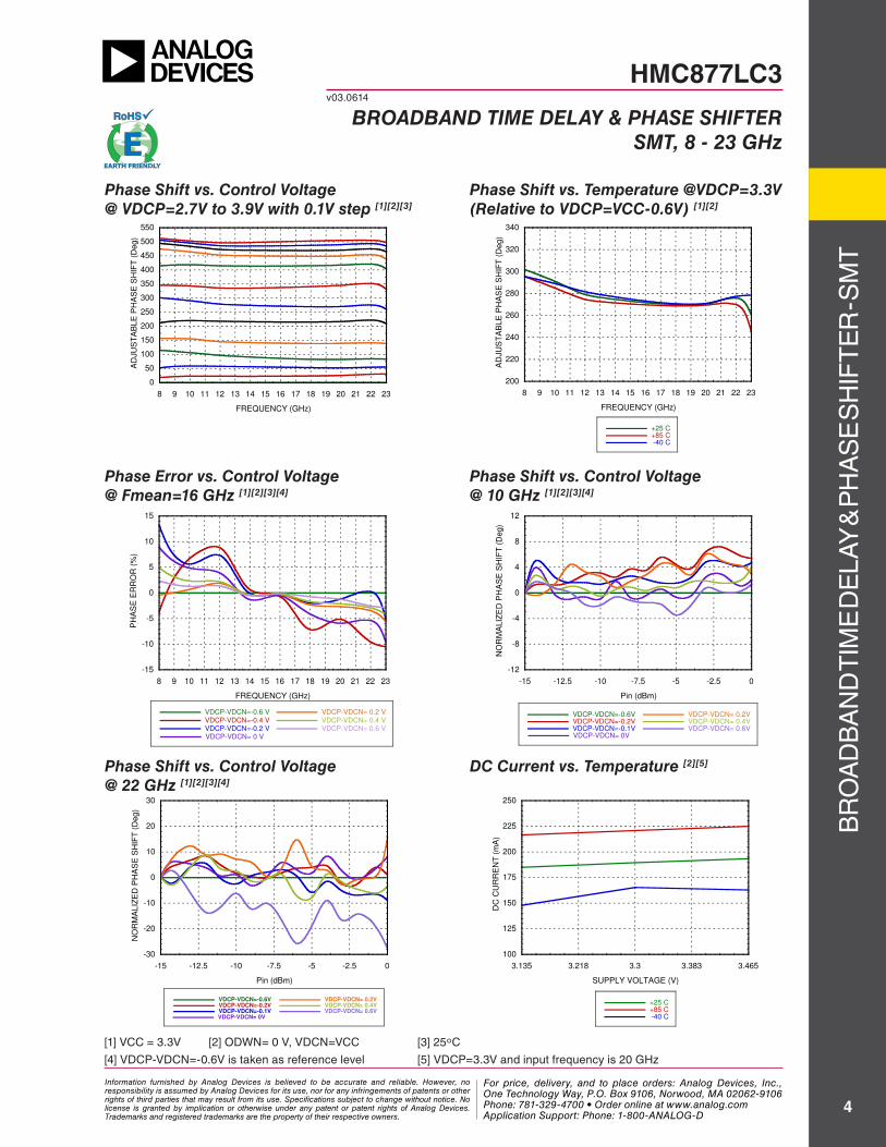
Phase Shift vs. Temperature @VDCP=3.3V (Relative to VDCP=VCC-0.6V) [1][2]
200
220
240
260
280
300
320
340
8 9 10 11 12 13 14 15 16 17 18 19 20 21 22 23
+25 C+85 C -40 C
AD
JU
ST
AB
LE
PH
AS
E S
HIF
T (
Deg)
FREQUENCY (GHz)
Phase Error vs. Control Voltage @ Fmean=16 GHz [1][2][3][4]
-15
-10
-5
0
5
10
15
8 9 10 11 12 13 14 15 16 17 18 19 20 21 22 23
VDCP-VDCN=-0.6 VVDCP-VDCN=-0.4 VVDCP-VDCN=-0.2 VVDCP-VDCN= 0 V
VDCP-VDCN= 0.2 VVDCP-VDCN= 0.4 VVDCP-VDCN= 0.6 V
PH
AS
E E
RR
OR
(%
)
FREQUENCY (GHz)
Phase Shift vs. Control Voltage @ 10 GHz [1][2][3][4]
-12
-8
-4
0
4
8
12
-15 -12.5 -10 -7.5 -5 -2.5 0
VDCP-VDCN=-0.6VVDCP-VDCN=-0.2VVDCP-VDCN=-0.1VVDCP-VDCN= 0V
VDCP-VDCN= 0.2VVDCP-VDCN= 0.4VVDCP-VDCN= 0.6V
NO
RM
ALIZ
ED
PH
AS
E S
HIF
T (
Deg)
Pin (dBm)
Phase Shift vs. Control Voltage@ 22 GHz [1][2][3][4]
-30
-20
-10
0
10
20
30
-15 -12.5 -10 -7.5 -5 -2.5 0
VDCP-VDCN=-0.6V
VDCP-VDCN=-0.2V
VDCP-VDCN=-0.1V
VDCP-VDCN= 0V
VDCP-VDCN= 0.2V
VDCP-VDCN= 0.4V
VDCP-VDCN= 0.6V
NO
RM
ALIZ
ED
PH
AS
E S
HIF
T (
Deg)
Pin (dBm)
[1] VCC = 3.3V [2] ODWN= 0 V, VDCN=VCC [3] 25°C
[4] VDCP-VDCN=-0.6V is taken as reference level [5] VDCP=3.3V and input frequency is 20 GHz
DC Current vs. Temperature [2][5]
100
125
150
175
200
225
250
3.135 3.218 3.3 3.383 3.465
+25 C+85 C -40 C
DC
CU
RR
EN
T (
mA
)
SUPPLY VOLTAGE (V)
Information furnished by Analog Devices is believed to be accurate and reliable. However, no responsibility is assumed by Analog Devices for its use, nor for any infringements of patents or other rights of third parties that may result from its use. Specifications subject to change without notice. No license is granted by implication or otherwise under any patent or patent rights of Analog Devices. Trademarks and registered trademarks are the property of their respective owners.
For price, delivery, and to place orders: Analog Devices, Inc., One Technology Way, P.O. Box 9106, Norwood, MA 02062-9106 Phone: 781-329-4700 • Order online at www.analog.com Application Support: Phone: 1-800-ANALOG-D

For price, delivery and to place orders: Hittite Microwave Corporation, 2 Elizabeth Drive, Chelmsford, MA 01824Phone: 978-250-3343 Fax: 978-250-3373 Order On-line at www.hittite.com
Application Support: Phone: 978-250-3343 or [email protected]
BR
OA
DB
AN
D T
IME
DE
LAY
& P
HA
SE
SH
IFT
ER
- SM
T
5
HMC877LC3v03.0614
BROADBAND TIME DELAY & PHASE SHIFTERSMT, 8 - 23 GHz
Single-Ended Output Swing vs. Frequency [1][3][4]
Single-Ended Output Swing vs. Supply Voltage [1][2][3]
340
360
380
400
420
440
460
480
500
3.135 3.3 3.465
+25 C+85 C -40 C
OU
TP
UT
VO
LT
AG
E (
mV
p-p
)
SUPPLY VOLTAGE (V)
300
350
400
450
500
550
600
8 9 10 11 12 13 14 15 16 17 18 19 20 21 22 23
+25 C+85 C -40 C
OU
TP
UT
VO
LT
AG
E (
mV
p-p
)
FREQUENCY (GHz)
Single-Ended Output Swing vs. Control Voltage [1][4][5]
250
300
350
400
450
500
550
600
-0.6 -0.4 -0.2 0 0.2 0.4 0.6
10 GHz16 GHz22 GHz
OU
TP
UT
VO
LT
AG
E (
mV
p-p
)
DIFFERENTIAL CONTROL VOLTAGE (V)
Duty Cycle Distortion @ 16 GHz [1][4][5]
40
45
50
55
60
-0.6 -0.4 -0.2 0 0.2 0.4 0.6
+25 C+85 C -40 C
DU
TY
CY
CLE
(%
)
DIFFERENTIAL CONTROL VOLTAGE (V)
[1] ODWN= 0V, VDCN=VCC [2] Input Frequency: 20 GHz [3] VDCP=3.3V [4] VCC=3.3V [5] On the x-axis differential control voltage represents VDCP-VDCN voltage[6] The input frequency is 10 GHz
Single-Ended Output Swing vs. Amplitude Control Voltage [1][3][4][6]
0
100
200
300
400
500
600
700
800
0.6 0.8 1 1.2 1.4 1.6 1.8
+25 C+85 C -40 C
OU
TP
UT
VO
LT
AG
E (
mV
p-p
)
AMPLITUDE CONTROL VOLTAGE (V)
Information furnished by Analog Devices is believed to be accurate and reliable. However, no responsibility is assumed by Analog Devices for its use, nor for any infringements of patents or other rights of third parties that may result from its use. Specifications subject to change without notice. No license is granted by implication or otherwise under any patent or patent rights of Analog Devices. Trademarks and registered trademarks are the property of their respective owners.
For price, delivery, and to place orders: Analog Devices, Inc., One Technology Way, P.O. Box 9106, Norwood, MA 02062-9106 Phone: 781-329-4700 • Order online at www.analog.com Application Support: Phone: 1-800-ANALOG-D

For price, delivery and to place orders: Hittite Microwave Corporation, 2 Elizabeth Drive, Chelmsford, MA 01824Phone: 978-250-3343 Fax: 978-250-3373 Order On-line at www.hittite.com
Application Support: Phone: 978-250-3343 or [email protected]
BR
OA
DB
AN
D T
IME
DE
LAY
& P
HA
SE
SH
IFT
ER
- SM
T
6
HMC877LC3v03.0614
BROADBAND TIME DELAY & PHASE SHIFTERSMT, 8 - 23 GHz
RMS Jitter vs. Temperature@ 16 GHz[1][2][3][4]
RMS Jitter vs. Bias Voltage@ 16 GHz [1][3][4]
0
0.1
0.2
0.3
0.4
0.5
0.6
0.7
0.8
0.9
-0.6 -0.4 -0.2 0 0.2 0.4 0.6
+25 C+85 C -40 C
RM
S J
ITT
ER
(ps)
DIFFERENTIAL CONTROL VOLTAGE (V)
0
0.1
0.2
0.3
0.4
0.5
0.6
0.7
0.8
0.9
-0.6 -0.4 -0.2 0 0.2 0.4 0.6
3.135 V 3.3 V
3.465 V
RM
S J
ITT
ER
(ps)
DIFFERENTIAL CONTROL VOLTAGE (V)
Fall Time vs.Temperature @ 16 GHz [1][2][3]
Rise Time vs.Temperature @ 16 GHz [1][2][3]
5
7.5
10
12.5
15
-0.6 -0.4 -0.2 0 0.2 0.4 0.6
+25 C+85 C -40 C
RIS
E T
IME
(ps)
DIFFERENTIAL CONTROL VOLTAGE (V)
5
7.5
10
12.5
15
-0.6 -0.4 -0.2 0 0.2 0.4 0.6
+25 C+85 C -40 C
FA
LL T
IME
(ps)
DIFFERENTIAL CONTROL VOLTAGE (V)
[1] ODWN= 0V, VDCN=VCC [2] VCC=3.3V [3] On the x-axis differential control voltage represents VDCP-VDCN voltage [4] Source jitter was not deembeded[5] fin is the fundemental frequency
Pfin-Pfin/2 Output Power Difference vs. Control Voltage [1][2][5]
0
10
20
30
40
50
8 9 10 11 12 13 14 15 16 17 18 19 20 21 22 23
VDCP-VDCN=-0.6VVDCP-VDCN=-0.4VVDCP-VDCN=-0.2VVDCP-VDCN= 0V
VDCP-VDCN= 0.2VVDCP-VDCN= 0.4VVDCP-VDCN= 0.6V
Pfin-P
fin/2 (d
Bc)
FREQUENCY (GHz)
Pfin-P3fin/2 Output Power Difference vs. Control Voltage [1][2][5]
0
10
20
30
40
50
60
8 9 10 11 12 13 14 15 16 17 18 19 20 21 22 23
VDCP-VDCN=-0.6VVDCP-VDCN=-0.4VVDCP-VDCN=-0.2VVDCP-VDCN= 0V
VDCP-VDCN= 0.2VVDCP-VDCN= 0.4VVDCP-VDCN= 0.6V
Pfin-P
3fin/2 (d
Bc)
FREQUENCY (GHz)
Information furnished by Analog Devices is believed to be accurate and reliable. However, no responsibility is assumed by Analog Devices for its use, nor for any infringements of patents or other rights of third parties that may result from its use. Specifications subject to change without notice. No license is granted by implication or otherwise under any patent or patent rights of Analog Devices. Trademarks and registered trademarks are the property of their respective owners.
For price, delivery, and to place orders: Analog Devices, Inc., One Technology Way, P.O. Box 9106, Norwood, MA 02062-9106 Phone: 781-329-4700 • Order online at www.analog.com Application Support: Phone: 1-800-ANALOG-D

For price, delivery and to place orders: Hittite Microwave Corporation, 2 Elizabeth Drive, Chelmsford, MA 01824Phone: 978-250-3343 Fax: 978-250-3373 Order On-line at www.hittite.com
Application Support: Phone: 978-250-3343 or [email protected]
BR
OA
DB
AN
D T
IME
DE
LAY
& P
HA
SE
SH
IFT
ER
- SM
T
7
HMC877LC3v03.0614
BROADBAND TIME DELAY & PHASE SHIFTERSMT, 8 - 23 GHz
Input Return Loss vs. Frequency [1][4]
-45
-40
-35
-30
-25
-20
-15
-10
-5
0
0 2 4 6 8 10 12 14 16 18 20 22 24 26 28 30
INNINP
RE
TU
RN
LO
SS
(dB
)
FREQUENCY (GHz)
Output Return Loss vs. Frequency [1][4]
-45
-40
-35
-30
-25
-20
-15
-10
-5
0
0 2 4 6 8 10 12 14 16 18 20 22 24 26 28 30
QNQP
RE
TU
RN
LO
SS
(dB
)
FREQUENCY (GHz)
[1] VCC= 3.3 V, ODWN=0V [2] fin is the fundemental frequency[3] -6.8 dBm input power was applied to VDCP, VDCN is 50 Ohms terminated and fin=15 GHz [4] VDCP=VDCN=VCC
Modulation Signal Bandwidthvs. Temperature [1][3]
0
0.2
0.4
0.6
0.8
1
1.2
100 1000 10000
+25 C+85 C -40 C
PH
AS
E M
OD
ULA
TIO
N A
MP
LIT
UD
E (
UI)
FREQUENCY (MHz)
Second Harmonic vs. Control Voltage [1][2]
0
5
10
15
20
25
30
35
40
45
8 9 10 11 12 13 14 15 16 17 18 19 20 21 22 23
VDCP-VDCN=-0.6VVDCP-VDCN=-0.4VVDCP-VDCN=-0.2VVDCP-VDCN= 0V
VDCP-VDCN= 0.2VVDCP-VDCN= 0.4VVDCP-VDCN= 0.6V
Pfin-P
2fin (d
Bc)
FREQUENCY (GHz)
Information furnished by Analog Devices is believed to be accurate and reliable. However, no responsibility is assumed by Analog Devices for its use, nor for any infringements of patents or other rights of third parties that may result from its use. Specifications subject to change without notice. No license is granted by implication or otherwise under any patent or patent rights of Analog Devices. Trademarks and registered trademarks are the property of their respective owners.
For price, delivery, and to place orders: Analog Devices, Inc., One Technology Way, P.O. Box 9106, Norwood, MA 02062-9106 Phone: 781-329-4700 • Order online at www.analog.com Application Support: Phone: 1-800-ANALOG-D

For price, delivery and to place orders: Hittite Microwave Corporation, 2 Elizabeth Drive, Chelmsford, MA 01824Phone: 978-250-3343 Fax: 978-250-3373 Order On-line at www.hittite.com
Application Support: Phone: 978-250-3343 or [email protected]
BR
OA
DB
AN
D T
IME
DE
LAY
& P
HA
SE
SH
IFT
ER
- SM
T
8
HMC877LC3v03.0614
BROADBAND TIME DELAY & PHASE SHIFTERSMT, 8 - 23 GHz
Output Eye Diagram Snapshot for 15 GHz Input SignalTime Scale: 10 ps/div
Amplitude Scale: 81.8 mV/div
Test Conditions:
VCC=3.3 V, ODWN=0 V
VDCP = 300 mVpp @ 1 MHz
VDCN is 50 Ohms terminated
Measurement Results:
RMS Jitter: 0.3 ps
Peak to peak Jitter: 1.78 ps
Rise Time: 11.78 ps
Fall Time: 11.78 ps
Output Eye Diagram Continuous Snapshot for 15 GHz Input Signal
Time Scale: 10 ps/div
Amplitude Scale: 81.8 mV/div
Test Conditions:
VCC=3.3 V, ODWN=0 V
VDCP = 300 mVpp @ 1 MHz
VDCN is 50 Ohms terminated
Measurement Result:
26.8 ps (0.4 UI )
Information furnished by Analog Devices is believed to be accurate and reliable. However, no responsibility is assumed by Analog Devices for its use, nor for any infringements of patents or other rights of third parties that may result from its use. Specifications subject to change without notice. No license is granted by implication or otherwise under any patent or patent rights of Analog Devices. Trademarks and registered trademarks are the property of their respective owners.
For price, delivery, and to place orders: Analog Devices, Inc., One Technology Way, P.O. Box 9106, Norwood, MA 02062-9106 Phone: 781-329-4700 • Order online at www.analog.com Application Support: Phone: 1-800-ANALOG-D

For price, delivery and to place orders: Hittite Microwave Corporation, 2 Elizabeth Drive, Chelmsford, MA 01824Phone: 978-250-3343 Fax: 978-250-3373 Order On-line at www.hittite.com
Application Support: Phone: 978-250-3343 or [email protected]
BR
OA
DB
AN
D T
IME
DE
LAY
& P
HA
SE
SH
IFT
ER
- SM
T
9
HMC877LC3v03.0614
BROADBAND TIME DELAY & PHASE SHIFTERSMT, 8 - 23 GHz
Absolute Maximum RatingsPower Supply Voltage (Vcc) -0.5V to +3.75V
Input Voltage (VIN),Output Voltage (VOUT)
Vcc -1.2V to Vcc+0.6V
Control Voltage (VDCP), Delay Control Voltage Range Adjustment (LC),Amplitude Control Voltage (VAC)
0 to Vcc+0.6V
Channel Temperature (Tc) 125 °C
Continuous Pdiss (T = 85 °C)(derate 35.8 mW/°C above 85 °C)
1.43 W
Thermal Resistance(junction to ground paddle)
27.9 °C/W
Storage Temperature -65 to +125 °C
Operating Temperature -40 to +85°C
ESD Sensitivity (HBM) Class 1A
ELECTROSTATIC SENSITIVE DEVICEOBSERVE HANDLING PRECAUTIONS
Information furnished by Analog Devices is believed to be accurate and reliable. However, no responsibility is assumed by Analog Devices for its use, nor for any infringements of patents or other rights of third parties that may result from its use. Specifications subject to change without notice. No license is granted by implication or otherwise under any patent or patent rights of Analog Devices. Trademarks and registered trademarks are the property of their respective owners.
For price, delivery, and to place orders: Analog Devices, Inc., One Technology Way, P.O. Box 9106, Norwood, MA 02062-9106 Phone: 781-329-4700 • Order online at www.analog.com Application Support: Phone: 1-800-ANALOG-D

For price, delivery and to place orders: Hittite Microwave Corporation, 2 Elizabeth Drive, Chelmsford, MA 01824Phone: 978-250-3343 Fax: 978-250-3373 Order On-line at www.hittite.com
Application Support: Phone: 978-250-3343 or [email protected]
BR
OA
DB
AN
D T
IME
DE
LAY
& P
HA
SE
SH
IFT
ER
- SM
T
10
HMC877LC3v03.0614
BROADBAND TIME DELAY & PHASE SHIFTERSMT, 8 - 23 GHz
Outline Drawing
NOTES:1. PACKAGE BODY MATERIAL: ALUMINA2. LEAD AND GROUND PADDLE PLATING: 30-80 MICROINCHES GOLD OVER 50 MICRO-INCHES MINIMUM NICKEL.3. DIMENSIONS ARE IN INCHES [MILLIMETERS].4. LEAD SPACING TOLERANCE IS NON-CUMULATIVE.5. CHARACTERS TO BE BLACK INK MARKED WITH .018”MIN to .030”MAX HEIGHT REQUIREMENTS. UTILIZE MAXIMUM CHARACTER HEIGHT BASED ON LID DIMENSIONS AND BEST FIT. LOCATE APPROX. AS SHOWN.6. PACKAGE WARP SHALL NOT EXCEED 0.05mm DATUM -C-7. ALL GROUND LEADS AND GROUND PADDLE MUST BE SOLDERED TO PCB RF GROUND.
Package Information
Part Number Package Body Material Lead Finish MSL Rating Package Marking [2]
HMC877LC3 Alumina, White Gold over Nickel MSL3 [1] H877XXXX
[1] Max peak reflow temperature of 260 °C[2] 4-Digit lot number XXXX
Information furnished by Analog Devices is believed to be accurate and reliable. However, no responsibility is assumed by Analog Devices for its use, nor for any infringements of patents or other rights of third parties that may result from its use. Specifications subject to change without notice. No license is granted by implication or otherwise under any patent or patent rights of Analog Devices. Trademarks and registered trademarks are the property of their respective owners.
For price, delivery, and to place orders: Analog Devices, Inc., One Technology Way, P.O. Box 9106, Norwood, MA 02062-9106 Phone: 781-329-4700 • Order online at www.analog.com Application Support: Phone: 1-800-ANALOG-D

For price, delivery and to place orders: Hittite Microwave Corporation, 2 Elizabeth Drive, Chelmsford, MA 01824Phone: 978-250-3343 Fax: 978-250-3373 Order On-line at www.hittite.com
Application Support: Phone: 978-250-3343 or [email protected]
BR
OA
DB
AN
D T
IME
DE
LAY
& P
HA
SE
SH
IFT
ER
- SM
T
11
HMC877LC3v03.0614
BROADBAND TIME DELAY & PHASE SHIFTERSMT, 8 - 23 GHz
Pin Number Function Description Interface Schematic
1, 4-5, 8-9,12 GNDSignal grounds should be connected to 0V.
Ground paddle must be connected to DC ground
2, 3, 6, 7
INPINN
VDCPVDCN
Differential signal inputs.
10, 11QNQP
Differential signal outputs.
13 VAC The output amplitude control pin.
14 ODWNEnable pin of the output. It should be connected to GND to enable the part. When it is connected to VCC or floated the output is set
to VCC.
15 VCC The supply voltage of the part.
Pin Descriptions
Information furnished by Analog Devices is believed to be accurate and reliable. However, no responsibility is assumed by Analog Devices for its use, nor for any infringements of patents or other rights of third parties that may result from its use. Specifications subject to change without notice. No license is granted by implication or otherwise under any patent or patent rights of Analog Devices. Trademarks and registered trademarks are the property of their respective owners.
For price, delivery, and to place orders: Analog Devices, Inc., One Technology Way, P.O. Box 9106, Norwood, MA 02062-9106 Phone: 781-329-4700 • Order online at www.analog.com Application Support: Phone: 1-800-ANALOG-D

For price, delivery and to place orders: Hittite Microwave Corporation, 2 Elizabeth Drive, Chelmsford, MA 01824Phone: 978-250-3343 Fax: 978-250-3373 Order On-line at www.hittite.com
Application Support: Phone: 978-250-3343 or [email protected]
BR
OA
DB
AN
D T
IME
DE
LAY
& P
HA
SE
SH
IFT
ER
- SM
T
12
HMC877LC3v03.0614
BROADBAND TIME DELAY & PHASE SHIFTERSMT, 8 - 23 GHz
Pin Number Function Description Interface Schematic
16 LC
This pin enables the control of the linearity level of Control Voltage vs. Phase Shift/Time Delay. Compromise is between linearity level
and wideness of the Phase Shift/Time Delay tuning range. For optimum tuning range and linearity balance, R2=R3 are chosen as
4.7 kOhms.
Pin Descriptions (Continued)
Application Circuit
Information furnished by Analog Devices is believed to be accurate and reliable. However, no responsibility is assumed by Analog Devices for its use, nor for any infringements of patents or other rights of third parties that may result from its use. Specifications subject to change without notice. No license is granted by implication or otherwise under any patent or patent rights of Analog Devices. Trademarks and registered trademarks are the property of their respective owners.
For price, delivery, and to place orders: Analog Devices, Inc., One Technology Way, P.O. Box 9106, Norwood, MA 02062-9106 Phone: 781-329-4700 • Order online at www.analog.com Application Support: Phone: 1-800-ANALOG-D

For price, delivery and to place orders: Hittite Microwave Corporation, 2 Elizabeth Drive, Chelmsford, MA 01824Phone: 978-250-3343 Fax: 978-250-3373 Order On-line at www.hittite.com
Application Support: Phone: 978-250-3343 or [email protected]
BR
OA
DB
AN
D T
IME
DE
LAY
& P
HA
SE
SH
IFT
ER
- SM
T
13
HMC877LC3v03.0614
BROADBAND TIME DELAY & PHASE SHIFTERSMT, 8 - 23 GHz
Evaluation PCB
The circuit board used in the application should use RF circuit design techniques. Signal lines should have 50 Ohm impedance while the package ground leads and exposed paddle should be con-nected directly to the ground plane similar to that shown. A sufficient number of via holes should be used to connect the top and bottom ground planes. The evaluation board should be mounted to an appropriate heat sink. The evaluation circuit board shown is available from Hittite upon request.
List of Materials for Evaluation PCB EVAL01-HMC877LC3[1]
Item Description
J1 - J2, J5-J6 K Connector
J3-J4 SMA Connector
TP1-TP5 DC Pin
C1-C3 1000 pF Capacitor, 0402 Pkg.
C5-C7 0.1 µF Capacitor, 0402 Pkg.
C8-C9 4.7 µF Capacitor, Tantalum
R2-R3 4.7 kOhm Resistor, 0402 Pkg.
U1HMC877LC3 Analog Phase Shifter/Broadband Time Delay
PCB [2] 600-00064-00 Evaluation Board
[1] Reference this number when ordering complete evaluation PCB
[2] Circuit Board Material: Rogers 4350 or Arlon 25 FR
Information furnished by Analog Devices is believed to be accurate and reliable. However, no responsibility is assumed by Analog Devices for its use, nor for any infringements of patents or other rights of third parties that may result from its use. Specifications subject to change without notice. No license is granted by implication or otherwise under any patent or patent rights of Analog Devices. Trademarks and registered trademarks are the property of their respective owners.
For price, delivery, and to place orders: Analog Devices, Inc., One Technology Way, P.O. Box 9106, Norwood, MA 02062-9106 Phone: 781-329-4700 • Order online at www.analog.com Application Support: Phone: 1-800-ANALOG-D

For price, delivery and to place orders: Hittite Microwave Corporation, 2 Elizabeth Drive, Chelmsford, MA 01824Phone: 978-250-3343 Fax: 978-250-3373 Order On-line at www.hittite.com
Application Support: Phone: 978-250-3343 or [email protected]
BR
OA
DB
AN
D T
IME
DE
LAY
& P
HA
SE
SH
IFT
ER
- SM
T
14
HMC877LC3v03.0614
BROADBAND TIME DELAY & PHASE SHIFTERSMT, 8 - 23 GHz
Information furnished by Analog Devices is believed to be accurate and reliable. However, no responsibility is assumed by Analog Devices for its use, nor for any infringements of patents or other rights of third parties that may result from its use. Specifications subject to change without notice. No license is granted by implication or otherwise under any patent or patent rights of Analog Devices. Trademarks and registered trademarks are the property of their respective owners.
For price, delivery, and to place orders: Analog Devices, Inc., One Technology Way, P.O. Box 9106, Norwood, MA 02062-9106 Phone: 781-329-4700 • Order online at www.analog.com Application Support: Phone: 1-800-ANALOG-D