Embed Size (px)
Citation preview

High Density, High Reliability Carbon Nanotube NRAM
Thomas Rueckes CTO
Nantero

Nantero Overview
§ Founded in 2001 to develop nonvolatile memory using carbon nanotubes (CNT) for high density standalone and embedded applications • CNT engineering in Boston • Circuit design, product, test, device & integration engineering in Sunnyvale • Government Business sold to Lockheed Martin in 2008 & successful NRAM test
on space shuttle mission • Commercial development partnerships with IDMs & fabless companies for
embedded and standalone memory applications in progress
§ Technology development & IP licensing business model • >133 US patents awarded, >205 US applications pending, plus more worldwide • WSJ patent score card:
– The only semiconductor start-up ranked (2009) – #2 ranked for scientific strength of IP (2010)
• IEEE Spectrum; Semiconductor Manufacturing Category – #5 worldwide (2009) – #2 worldwide and #1 in US (2010)

Nantero Timeline
2001 2002 2003 2004 2005 2006 2007 2008 2009 2010
First Patterned CNT Fabric
First NRAM Switch
First CMOS integration in production fab
First Fab compatible CNT formulation
First fully integrated CNT IC
First 22nm NRAM Switch
Nantero
GBU sold To LM
NRAM 4M IC on-board Space Shuttle Mission
Commercial produ
ct joint
developm
ent p
artnerships

NRAM: RRAM with CNT Resistance Change Material
ELECTRODE
ELECTRODE
-‐RESET (ON à OFF): CNT-‐to-‐CNT are not in physical contact = high resistance -‐SET (OFF à ON): CNT are in physical contact = low resistance
SET is an electrostaCc operaCon while RESET is phonon driven operaCon (phonon heaCng of CNT contacts)
OFF (‘0’)
ON (‘1’) W
W
TiN
CNT
Cross section

NRAM Mechanism
§ SET: electrostatic operation • Write voltage à electrostatic CNT-CNT attraction à CNT junction closure (ON)
• CNTs remain in ON state due to physical adhesion (Eact ~ 5eV)
+-
Electro-static SET
§ RESET: phonon driven operation • Voltage applied à CNT phonon excitation à CNT separation (OFF)
• CNTs remain in OFF state due to high mechanical (1TPa) stiffness (Eact>>5eV)
Phonon RESET
Phonon excitation

CNT Process Integration
-CNT Spin-on foundry capability at SVTC on 300mm & 200mm coat tracks
-Tracemetals meets typical BEOL contamination specs (TXRF: <1E11/cm2)
-CNT wafers being processed using 248nm,
193nm dry & immersion lithography -CNT Integration temperatures at standard 425C
BEOL and higher if W interconnect only -Conventional tooling for CNT RIE dry etch and
post etch cleaning -CNT density controllable for different technology
nodes
Aligned CNT film for <2X nm (top down SEM)
Spin-coated CNT film (top down SEM)
1M CORE
1M CORE
1M CORE
1M CORE
IO, COL SEL
ROW DEC
LOGIC, BUFFERS, TEST
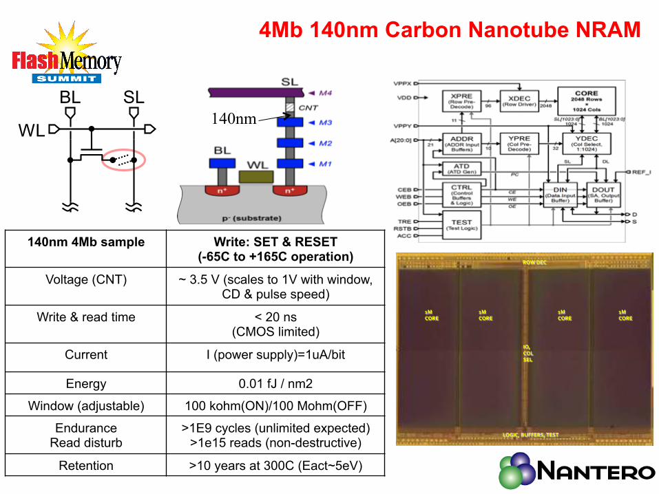
WL
BL SL
140nm 4Mb sample Write: SET & RESET (-65C to +165C operation)
Voltage (CNT) ~ 3.5 V (scales to 1V with window, CD & pulse speed)
Write & read time < 20 ns (CMOS limited)
Current I (power supply)=1uA/bit
Energy 0.01 fJ / nm2
Window (adjustable) 100 kohm(ON)/100 Mohm(OFF)
Endurance Read disturb
>1E9 cycles (unlimited expected) >1e15 reads (non-destructive)
Retention >10 years at 300C (Eact~5eV)
140nm
4Mb 140nm Carbon Nanotube NRAM

NRAM Devices at 99.997% Yield
• -93% of the word lines at 100% bit yield (complete 1Mb bank; 512WLs, 2kb each)
• only ~30 bits in 1Mb bank failing (all in 1st cycle)
• No bit fallouts during cycling
• Total bit yield is 99.997%
• Redundancy adequate to repair the device
Column number (0-2048)
row
num
ber (
0-51
2)

NRAM Data Retention: >10 Years @ 300C
Icell (in µA) at 1volt
T0= before bake T1= after 1 hour bake T4= after 4 hour bake T24= after 24 hour bake T48= after 48 hour bake T96= after 96 hour bake T168=after 168 hour bake *
32kbit / die for each temp
T0 T48
T0 T168
T0 T168
T0 T48
T0 T168
% b
its
85C 125C 200C 250C 300C
Data retention: >10years at 300C (3σ) Activation energy: 5.4eV(median), 4.5eV(3σ)

NRAM Endurance: >1E9 Cycles
Fixed Voltage & pulse width cycling: 3.5V / 20nsec (SET & RESET) >1 billion cycles without window degradation Unlimited endurance expected based on mechanism
Cycle #
Rea
d cu
rren
t at 1
V in
nA
Stable window through >1B cycles
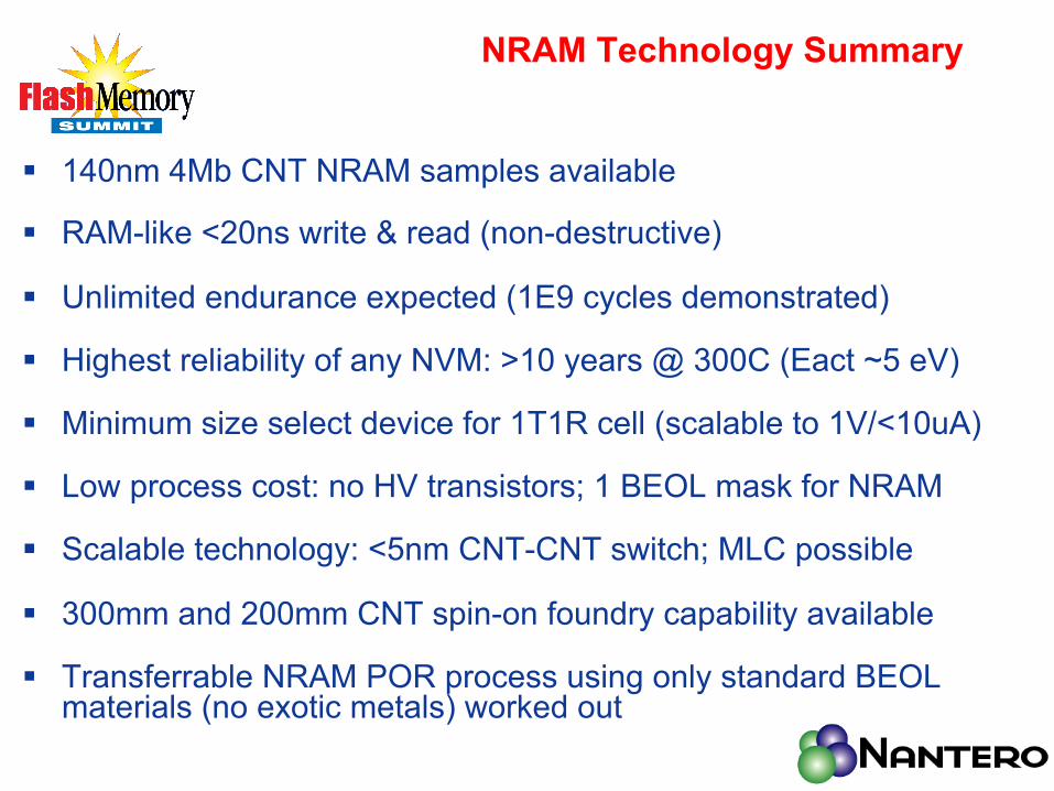
NRAM Technology Summary
§ 140nm 4Mb CNT NRAM samples available
§ RAM-like <20ns write & read (non-destructive)
§ Unlimited endurance expected (1E9 cycles demonstrated)
§ Highest reliability of any NVM: >10 years @ 300C (Eact ~5 eV)
§ Minimum size select device for 1T1R cell (scalable to 1V/<10uA)
§ Low process cost: no HV transistors; 1 BEOL mask for NRAM
§ Scalable technology: <5nm CNT-CNT switch; MLC possible
§ 300mm and 200mm CNT spin-on foundry capability available
§ Transferrable NRAM POR process using only standard BEOL materials (no exotic metals) worked out

NRAM Memory Applications
• NRAM for post-NAND • Scalability to
<5nm • Low write
current • Dense 1T1R
& 1D1R cells
• MLC capable
• NRAM for embedded NVM
• Low cost • Highest reliability • Competitive macro size • Scalability
• NRAM for post-DRAM • Scalability to
<5nm • High
endurance • Fast write
time • Low write
current