Embed Size (px)
Citation preview

5136-DNP-CPCI
Hardware Reference
Version 1.0
50 Northland Road, Waterloo, Ontario N2V 1N3(519) 725-5136 fax (519) 725-1515
© 1999 SST, a division of Woodhead Canada Limited.Printed in Canada
5136-DNP-CPCI Hardware Reference
© 1999 SST/Woodhead Canada Limited i
Publication Name : Publication Revision:
Date Printed:
dnp-cpci.doc1.07/21/99
© 1999 SST/Woodhead Canada LimitedSST is a trademark of Woodhead industries, Inc.
--This Document Applies To --5136-DNP-CPCI Interface Card

5136-DNP-CPCI Hardware Reference
© 1999 SST/Woodhead Canada Limited ii
Table of Contents
1. Introduction 1
1.1 Purpose of this Document 1
1.2 5136-DNP-CPCI Overview 1
2. Hardware Description 2
2.1 Overview 2
2.2 Connectors 2
2.2.1 CompactPCI Edge Connector 2
2.2.2 CAN Connector (CN1) 2
2.2.3 Test Points (TP1, TP2) 3
2.3 Indicators 3
2.3.1 Health Indicator 3
2.3.2 Health Indicator (Health) 3
2.3.3 Network Status Indicator (Comm) 3
3. Hardware Installation 4
3.1 Introduction 4
3.2 Installing the card 4
3.3 Connecting to a DeviceNet Network 4
3.3.1 Termination Resistor 4
3.4 Connecting to a CAN Network 5
3.4.1 Termination Resistor 5
3.4.2 Power 5
3.5 Grounding 5
4. Hardware Technical Information 6
4.1 Introduction 6
4.2 DeviceNet Pro Mode Register Interface 6
4.2.1 Card Command Register - CCM - Base Address + 0 6
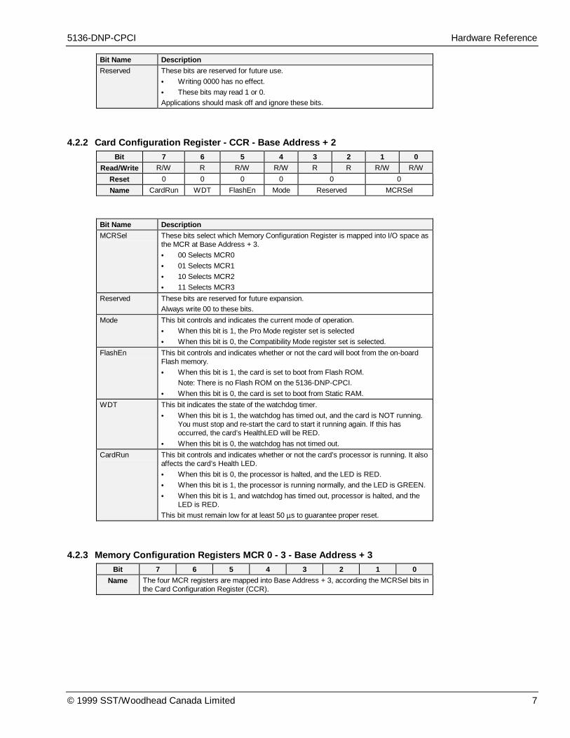
4.2.2 Card Configuration Register - CCR - Base Address + 2 7
4.2.3 Memory Configuration Registers MCR 0 - 3 - Base Address + 3 7
4.2.4 Memory Configuration Register 0 - MCR0 8
4.2.5 Memory Bank Selection 8
4.2.6 Memory Configuration Register 1 - MCR1 8
4.2.7 Memory Configuration Register 2 - MCR2 9
4.2.8 Memory Configuration Register 3 - MCR3 9
4.2.9 Interrupt Configuration Register - ICR - Base Address + 4 9
4.2.10 Identification Register - IDR - Base Address + 7 10
5136-DNP-CPCI Hardware Reference
© 1999 SST/Woodhead Canada Limited iii
4.3 DeviceNet Compatibility Mode I/O Registers 10
4.3.1 Main Board Control Register - BCR0 - Base Address + 0 10
4.3.2 Loader/Memory Configuration Register - BCR1 - Base Address + 1 11
4.3.3 Loader/Memory Configuration Register - BCR2 - Base Address + 2 11
4.3.4 Identification Register - IDR - Base Address + 7 12
4.4 PCI Configuration 12
4.5 Application Module Header 13
4.5.1 Data Type Descriptions 13
4.5.2 Byte Ordering 13
4.5.3 Application Module Header 14
4.6 Loading an Application Module in Compatible Mode 15
4.6.1 Test for 5136-DNP-CPCI at I/O port address specified 15
4.6.2 Check for conflicting RAM 15
4.6.3 Enable and test the card RAM 15
4.6.4 Load the application module 15
4.6.5 Configure Interrupts 16
4.6.6 Start the application module 16
4.6.7 Check module startup results 16
4.6.8 Test Interrupt Generation 16
4.6.9 Successful completion 16
4.6.10 If something goes wrong 16
Appendix A Specifications 17
Appendix B Card Error Messages 18
Appendix C Technical Support 20
Appendix D Warranty 21
5136-DNP-CPCI Hardware Reference
© 1999 SST/Woodhead Canada Limited 1
1. Introduction
1.1 Purpose of this Document
This document is a hardware reference manual for the 5136-DNP-CPCI interface card.
The 5136-DNP-CPCI has its own CPU that executes downloadable application software modules. Each of thesesoftware modules has an accompanying manual that describes its operation.
1.2 5136-DNP-CPCI Overview
The 5136-DNP-CPCI is a CompactPCI interface card for communication with DeviceNet and other CAN-basednetworks.
The main features of the 5136-DNP-CPCI are:
• 33 MHz, 32 bit CompactPCI interface (fully compliant with PCI 2.1 Spec and CompactPCI 2.0 R2.1 spec)
• 40 MHz AM186EM microprocessor with 256K RAM
• 256K shared RAM
• Optically isolated CAN interface
• DeviceNet compatible 5-pin CAN connector
• DeviceNet compatible Network Status bicolor indicator
• Supports connection to non-powered (3 wire) CAN networks with external 12-24 VDC supply
• Compatible with CAN specification 2.0 part A
• Supports CAN data rates up to 1 Mbaud
• Supports standard DeviceNet data rates 125, 250 and 500 Kbaud
5136-DNP-CPCI Hardware Reference
© 1999 SST/Woodhead Canada Limited 2
2. Hardware Description
2.1 Overview
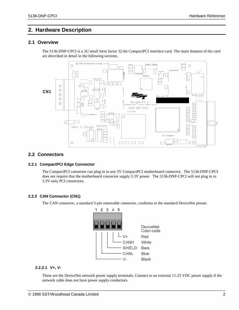
The 5136-DNP-CPCI is a 3U small form factor 32-bit CompactPCI interface card. The main features of the cardare described in detail in the following sections.
CN1
2.2 Connectors
2.2.1 CompactPCI Edge Connector
The CompactPCI connector can plug in to any 5V CompactPCI motherboard connector. The 5136-DNP-CPCIdoes not require that the motherboard connector supply 3.3V power. The 5136-DNP-CPCI will not plug in to3.3V-only PCI connectors.
2.2.2 CAN Connector (CN1)
The CAN connector, a standard 5-pin removable connector, conforms to the standard DeviceNet pinout.
2.2.2.1 V+, V-
These are the DeviceNet network power supply terminals. Connect to an external 11-25 VDC power supply if thenetwork cable does not have power supply conductors.
5136-DNP-CPCI Hardware Reference
© 1999 SST/Woodhead Canada Limited 3
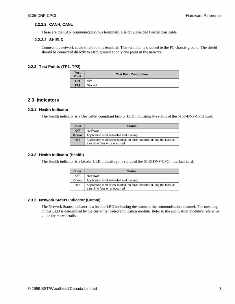
2.2.2.2 CANH, CANL
These are the CAN communication bus terminals. Use only shielded twisted pair cable.
2.2.2.3 SHIELD
Connect the network cable shield to this terminal. This terminal is snubbed to the PC chassis ground. The shieldshould be connected directly to earth ground at only one point in the network.
2.2.3 Test Points (TP1, TP2)TestPoint
Test Point Description
TP1 +5V
TP2 Ground
2.3 Indicators
2.3.1 Health Indicator
The Health indicator is a DeviceNet compliant bicolor LED indicating the status of the 5136-DNP-CPCI card.
Color Status
Off No Power
Green Application module loaded and running
Red Application module not loaded, an error occurred during the load, ora runtime fatal error occurred
2.3.2 Health Indicator ( Health)
The Health indicator is a bicolor LED indicating the status of the 5136-DNP-CPCI interface card.
Color Status
Off No Power
Green Application module loaded and running
Red Application module not loaded, an error occurred during the load, ora runtime fatal error occurred
2.3.3 Network Status Indicator (Comm)
The Network Status indicator is a bicolor LED indicating the status of the communication channel. The meaningof this LED is determined by the currently loaded application module. Refer to the application module’s referenceguide for more details.
5136-DNP-CPCI Hardware Reference
© 1999 SST/Woodhead Canada Limited 4
3. Hardware Installation
3.1 Introduction
This section describes the steps necessary to configure and install the 5136-DNP-CPCI.
The 5136-DNP-CPCI is plug-and-play compatible. No DIP-switches need to be set since all required memoryregions, I/O regions, and interrupts are automatically allocated by the Plug&Play BIOS.
3.2 Installing the card
To install the 5136-DNP-CPCI in your computer:
1. Turn the CompactPCI system off.
2. Wear an anti-static strap for the remaining steps.
If an anti-static strap is not available, leave the power cord connected and try to keep in contact with the metalcase of your CompactPCI system to eliminate the possibility of damaging the 5136-DNP-CPCI.
3. Locate an unused CompactPCI slot in your system.
4. Take the 5136-DNP-CPCI out of the anti-static bag, touching only the edges of the card. Do not touch theheader pins or the surface of the board.
5. Slide the 5136-DNP-CPCI card into an available slot in the CompactPCI system.
3.3 Connecting to a DeviceNet Network
Connect either a DeviceNet Trunk or Drop cable to the 5-pin connector according to the color code in section2.2.2. Make sure that all strands of wire go into the connector as bent strands may cause shorts to the adjacentterminal.
Directly connecting DeviceNet Trunk cable is not recommended due to the mechanical stress placed on theconnector by the heavy trunk cable. If you must attach trunk cable, secure it so no undue stress is placed on the5-pin connector.
3.3.1 Termination Resistor
The 5136-DNP-CPCI does not have a built-in termination resistor. If the card is at the extreme end of the network(end of trunk), connect a 120 ohm termination resistor from pin 2 to pin 4 of the 5-pin connector (providing thereare not already 2 terminators present on the network). This resistor can be inserted along with the DeviceNet cableprior to tightening the screws.
5136-DNP-CPCI Hardware Reference
© 1999 SST/Woodhead Canada Limited 5
3.4 Connecting to a CAN Network
Connect the CAN cable to the 5-pin connector and tighten all screws. Make sure that all strands of wire go into theconnector as bent strands may cause shorts to the adjacent terminal.
3.4.1 Termination Resistor
The 5136-DNP-CPCI does not have a built-in termination resistor. You must add termination in accordance withthe requirements of the target CAN network.
3.4.2 Power
If the CAN network does not supply 11-24 VDC power, connect an external power supply to the V+ and V- pinson the connector.
3.5 Grounding
The network shield should be connected directly to earth ground at only one point in the network.
5136-DNP-CPCI Hardware Reference
© 1999 SST/Woodhead Canada Limited 6
4. Hardware Technical Information
4.1 Introduction
This section provides technical hardware information. The information in this section is intended for programmersfamiliar with hardware-level PC programming.
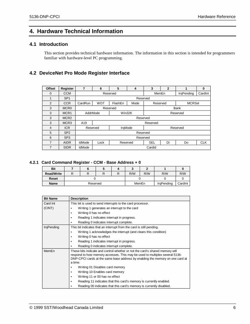
4.2 DeviceNet Pro Mode Register Interface
Offset Register 7 6 5 4 3 2 1 0
0 CCM Reserved MemEn IrqPending CardInt
1 SP1 Reserved
2 CCR CardRun WDT FlashEn Mode Reserved MCRSel
3 MCR0 Reserved Bank
3 MCR1 AddrMode Win32K Reserved
3 MCR2 Reserved
3 MCR3 A19 Reserved
4 ICR Reserved IrqMode Reserved
5 SP2 Reserved
6 SP3 Reserved
7 AIDR IdMode Lock Reserved SEL Di Do CLK
7 SIDR IdMode CardId
4.2.1 Card Command Register - CCM - Base Address + 0Bit 7 6 5 4 3 2 1 0
Read/Write R R R R R/W R/W R/W R/W
Reset 0 0 0 0
Name Reserved MemEn IrqPending CardInt
Bit Name Description
Card Int(CINT)
This bit is used to send interrupts to the card processor.
• Writing 1 generates an interrupt to the card
• Writing 0 has no effect
• Reading 1 indicates interrupt in progress.
• Reading 0 indicates interrupt complete.
IrqPending This bit indicates that an interrupt from the card is still pending.
• Writing 1 acknowledges the interrupt (and clears this condition)
• Writing 0 has no effect
• Reading 1 indicates interrupt in progress.
• Reading 0 indicates interrupt complete.
MemEn These bits indicate and control whether or not the card’s shared memory willrespond to host memory accesses. This may be used to multiplex several 5136-DNP-CPCI cards at the same base address by enabling the memory on one card ata time.
• Writing 01 Disables card memory
• Writing 10 Enables card memory
• Writing 11 or 00 has no effect
• Reading 11 indicates that this card’s memory is currently enabled.
• Reading 00 indicates that this card’s memory is currently disabled.
5136-DNP-CPCI Hardware Reference
© 1999 SST/Woodhead Canada Limited 7
Bit Name Description
Reserved These bits are reserved for future use.
• Writing 0000 has no effect.
• These bits may read 1 or 0.Applications should mask off and ignore these bits.
4.2.2 Card Conf iguration Register - CCR - Base Address + 2Bit 7 6 5 4 3 2 1 0
Read/Write R/W R R/W R/W R R R/W R/W
Reset 0 0 0 0 0 0
Name CardRun WDT FlashEn Mode Reserved MCRSel
Bit Name DescriptionMCRSel These bits select which Memory Configuration Register is mapped into I/O space as
the MCR at Base Address + 3.
• 00 Selects MCR0
• 01 Selects MCR1
• 10 Selects MCR2
• 11 Selects MCR3
Reserved These bits are reserved for future expansion.
Always write 00 to these bits.
Mode This bit controls and indicates the current mode of operation.
• When this bit is 1, the Pro Mode register set is selected
• When this bit is 0, the Compatibility Mode register set is selected.
FlashEn This bit controls and indicates whether or not the card will boot from the on-boardFlash memory.
• When this bit is 1, the card is set to boot from Flash ROM.Note: There is no Flash ROM on the 5136-DNP-CPCI.
• When this bit is 0, the card is set to boot from Static RAM.
WDT This bit indicates the state of the watchdog timer.
• When this bit is 1, the watchdog has timed out, and the card is NOT running.You must stop and re-start the card to start it running again. If this hasoccurred, the card’s HealthLED will be RED.
• When this bit is 0, the watchdog has not timed out.
CardRun This bit controls and indicates whether or not the card’s processor is running. It alsoaffects the card’s Health LED.
• When this bit is 0, the processor is halted, and the LED is RED.
• When this bit is 1, the processor is running normally, and the LED is GREEN.
• When this bit is 1, and watchdog has timed out, processor is halted, and theLED is RED.
This bit must remain low for at least 50 µs to guarantee proper reset.
4.2.3 Memory Configuration Regist ers MCR 0 - 3 - Base Address + 3Bit 7 6 5 4 3 2 1 0
Name The four MCR registers are mapped into Base Address + 3, according the MCRSel bits inthe Card Configuration Register (CCR).
5136-DNP-CPCI Hardware Reference
© 1999 SST/Woodhead Canada Limited 8
4.2.4 Memory Configuration Register 0 - MCR0
Bank Selection
Bit 7 6 5 4 3 2 1 0
Read/Write R R R R R/W R/W R/W R/W
Reset 0 0
Name Reserved Bank
Bit Name Description
Bank The 5136-DNP-CPCI has 256k of memory accessible to the host. These bits selectwhich bank of memory the host can access.
• In 16k mode the bank number may be 0 through 15 (or 0x0 - 0xF)
• In 32k mode the bank number may be 0 through 7.The primary host interface window is located in bank 0.Note that by setting the Bank to 0 and the Bank Size to 16K, all banks can be linearlyaccessed in the 256K window, Bank 0 being mapped to the lowest 16K through toBank 15 mapped to the highest 16K.See section 4.2.5.
Reserved These bits are reserved for future expansion.Always write 00 to these bits.
4.2.5 Memory Bank SelectionPro Mode Pro Mode Compatible
ModeCompatible
ModeComment*
16k Bank Size 32k Bank Size 16k Bank Size 32k Bank Size
0 0 3 0 Host Interface
1 0 2 0
2 1 1 1
3 1 0 1
4 2 N/A 2
5 2 N/A 2
6 3 N/A 3
7 3 N/A 3
8 4 N/A 4
9 4 N/A 4
10 5 N/A 5
11 5 N/A 5
12 6 4 6
13 6 5 6 Module Load
14 7 6 7 Region
15 7 7 7
*The shaded area is reserved for future use
4.2.6 Memory Configuration Register 1 - MCR1
Memory Mode
Bit 7 6 5 4 3 2 1 0
Read/Write R R R R/W R R R R
Reset 0 0 0 1 0
Name AddrMode Win32K Reserved
Bit Name Description

5136-DNP-CPCI Hardware Reference
© 1999 SST/Woodhead Canada Limited 9
Bit Name DescriptionReserved These bits are reserved for 32-bit address selection
Win32K These bits control and indicate the Memory Bank Size
• 00 Indicates a 16k Bank Size
• 01 Indicates a 32k Bank Size
• Other sizes are not supported by the 5136-DNP-CPCI at this time.
AddrMode These bits indicate the memory mode used by this card.
• 00 Indicates 20-bit addressing
• Other modes are not supported by the 5136-DNP-CPCI at this time.
4.2.7 Memory Configuration Register 2 - MCR2
Memory Address Selection
Bit 7 6 5 4 3 2 1 0
Read/Write R R R R R R R R
Reset 0
Name Reserved
Bit Name DescriptionReserved These bits are reserved for 32-bit and 24-bit address selection
4.2.8 Memory Configuration Register 3 - MCR3
Memory Address Selection
Bit 7 6 5 4 3 2 1 0
Read/Write R R/W R/W R/W R/W R/W R R
Reset 1 0 0 0 0 0 0 0
Name A19 Reserved
Bit Name DescriptionReserved These bits are reserved. Always write 0 to these locations.
A19 A19 must always be set to 1.
4.2.9 Interrupt Configuration Register - ICR - Base Address + 4Bit 7 6 5 4 3 2 1 0
Read/Write R R R/W R/W
Reset 0 0 0 0
Name Reserved IrqMode Reserved
Bit Name Description
IrqMode These bits determine the hardware interrupt mode
• 00 disables PCI interrupts
• 11 enables PCI interrupts
Reserved Reserved bits, always write 0.

5136-DNP-CPCI Hardware Reference
© 1999 SST/Woodhead Canada Limited 10
4.2.10 Identification Register - IDR - Base Address + 7Bit 7 6 5 4 3 2 1 0
Reset 1 0 1 0 0 0 0 0
Read/Write R/W R R R R R R R
SIDR Name IdMode CardId = 0x0D
Read/Write R/W R R R/W R/W R/W R R/W
AIDR Name IdMode Lock Reserved SEL Di Do CLK
Bit Name Description
IdMode This bit selects the functionality of the remaining bits in the ID Register.
• 1 selects Advanced ID Register (AIDR)
• 0 selects Simple ID Register (SIDR)
CardId This is a 7 bit unique card Identifier.
• A value of 0x0D indicates that this is a 5136-DNP-CPCI card.
CLK This bit controls the data clock to the card’s EEPROM.
Do This bit provides output data from the card’s EEPROM.
Di This bit is the input data to the card’s EEPROM.
Sel This bit controls the select pin on the card’s EEPROM. The Lock bit must be setbefore the Sel bit may be enabled.
Reserved These bits are reserved for future use. Always write 0.
Lock This bit is a semaphore between the card processor and the host. It determines whohas control of the EEPROM.
• Writing 1 indicates that the host would like control.
• Writing 0 indicates that the host no longer needs control.
• Reading 1 means that the host may have control.
• Reading 0 means that the host may NOT have control.
4.3 DeviceNet Compatibility Mode I/O Registers
Offset Register 7 6 5 4 3 2 1 0
0 BCR0 MemEn Bank IntEn IrqPending Reserved CardInt
1 BCR1 Win16K Reserved Reserved Reserved
2 BCR2 CardRun WDInh HealthGrn Mode Reserved
7 AIDR IdMode Lock Reserved SEL Di Do CLK
7 SIDR IdMode CardId
4.3.1 Main Board Control Register - BCR0 - Base Address + 0Bit 7 6 5 4 3 2 1 0
Read/Write R/W R/W R/W R/W R/W R/W R/W R/W
Reset 0 0 0 0 0 0
Name MemEn Bank IntEn IrqPending Reserved CardInt
Bit Name Description
CardInt(CINT)
This bit is used to send interrupts to the card processor.
• Writing 1 generates an interrupt to the card
• Writing 0 has no effect
• Reading 1 indicates interrupt in progress.
• Reading 0 indicates interrupt complete.

5136-DNP-CPCI Hardware Reference
© 1999 SST/Woodhead Canada Limited 11
Bit Name Description
Reserved This bit is read/write for backward compatibility.
This bit has no effect.
IrqPending
(IRQ) This bit indicates that an interrupt from the card is still pending.
• Writing 1 acknowledges the interrupt (and clears this condition)
• Writing 0 has no effect
• Reading 1 indicates interrupt in progress.
• Reading 0 indicates interrupt complete.
IntEn
(IRQE)• Writing 1 enables PCI interrupts
• Writing 0 disables PCI interrupts (the IrqPending flag still functions asdescribed)
Bank The 5136-DNP-CPCI has 256k of memory accessible to the host. These bits selectwhich bank of memory the host can access.
• In 16K mode the bank number may be 0 through 7.
• In 32K mode the bank number may be 0 through 7.
Note A: This means that in 16K mode, only one half of the card’s memory isaccessible. See the Memory Bank Selection table in section 4.2.5.
Note B: It is not necessary to use Memory Banks with the 5136-DNP-CPCI as theentire 256k can be linearly accessed. Banks are supported though for backwardcompatibility. See section 4.2.5.
MemEn
(MEN) These bits indicate and control whether or not the card’s shared memory willrespond to host memory accesses. This may be used to multiplex several5136-DNP cards at the same base address by enabling the memory on one card ata time.
• Writing 0 Disables card memory
• Writing 1 Enables card memory
4.3.2 Loader/Memory Configuration Register - BCR1 - Base Address + 1Bit 7 6 5 4 3 2 1 0
Read/Write R/W R/W R R/W R/W R/W R/W R/W
Reset 0 0 0 0 0 0 0 0
Name Win16K Reserved Reserved Reserved
Bit Name DescriptionReserved Bits 0-4 are are read/write for backward compatibility but perform no function. Bit 5
is read only, bit 6 is read/write for compatibility.
Win32K This bit controls and indicates the Memory Bank Size
• 0 indicates a 32K bank size
• 1 indicates a 16K bank size
4.3.3 Loader/Memory Configuration Register - BCR2 - Base Address + 2Bit 7 6 5 4 3 2 1 0
Read/Write R/W R/W R R/W R/W R/W R/W R/W
Reset 0 0 0 0 0
Name CardRun WDInh HealthGrn Mode Reserved
Bit Name DescriptionReserved These bits are Read/Write for backward compatibility, but perform no function on the
5136-DNP-CPCI.
Mode This bit controls and indicates the current mode of operation.
• When this bit is 1, the Pro Mode register set is selected
• When this bit is 0, the Compatibility Mode register set is selected.
5136-DNP-CPCI Hardware Reference
© 1999 SST/Woodhead Canada Limited 12
Bit Name Description
HealthGrn
(HLTH) This bit controls and indicates the state of the card’s health LED.
• When this bit is 1, and the watchdog has not timed out, the LED is green.
• When this bit is 0, the LED is red.
• When the watchdog has timed out, the LED is red.
WDInh
(WDI) This bit controls and indicates whether or not the card’s watchdog is enabled.
• When this bit is 0, the watchdog is enabled.
• When this bit is 1, the watchdog is inhibited.
CardRun
(RUN) This bit controls and indicates whether or not the card’s processor is running.
• When this bit is 0, the processor is halted.
• When this bit is 1, the processor is running, unless the watchdog has timedout.
This bit must remain low for at least 50 µs to guarantee proper reset.
4.3.4 Identification Register - IDR - Base Address + 7
IDR at Base Address + 7 is identical to that of ProMode. Refer to section 4.2.10.
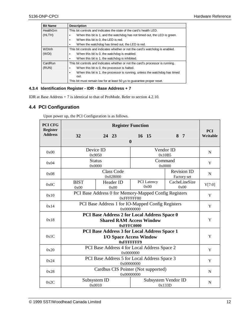
4.4 PCI Configuration
Upon power up, the PCI Configuration is as follows.
PCI CFGRegisterAddress
Register Function
32 24 23 16 15 8 70
PCIWritable
0x00 Device ID0x9050
Vendor ID0x10B5
N
0x04 Status0x0000
Command0x0000
Y
0x08 Class Code0x028000
Revision IDFactory set
N
0x0C BIST0x00
Header ID0x00
PCI Latency0x00
CacheLineSize0x00
Y[7:0]
0x10 PCI Base Address 0 for Memory-Mapped Config Registers0xFFFFFF80
Y
0x14 PCI Base Address 1 for IO-Mapped Config Registers0x00000000
Y
0x18PCI Base Address 2 for Local Address Space 0
Shared RAM Access Window0xFFFC0000
Y
0x1CPCI Base Address 3 for Local Address Space 1
I/O Space Access Window0xFFFFFFF9
Y
0x20 PCI Base Address 4 for Local Address Space 20x0000000
Y
0x24 PCI Base Address 5 for Local Address Space 30x00000000
Y
0x28 Cardbus CIS Pointer (Not supported)0x00000000
N
0x2C Subsystem ID0x0010
Subsystem Vendor ID0x133D
N
5136-DNP-CPCI Hardware Reference
© 1999 SST/Woodhead Canada Limited 13
PCI CFGRegisterAddress
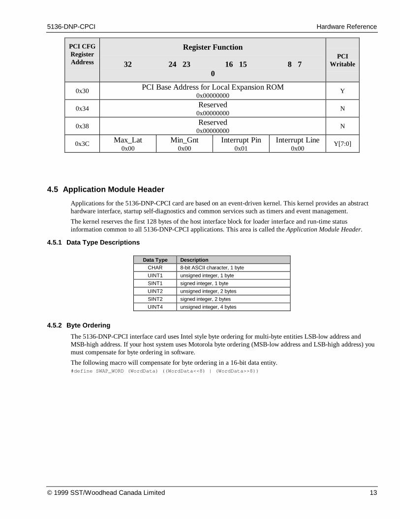
Register Function
32 24 23 16 15 8 70
PCIWritable
0x30 PCI Base Address for Local Expansion ROM0x00000000
Y
0x34 Reserved0x00000000
N
0x38 Reserved0x00000000
N
0x3C Max_Lat0x00
Min_Gnt0x00
Interrupt Pin0x01
Interrupt Line0x00
Y[7:0]
4.5 Application Module Header
Applications for the 5136-DNP-CPCI card are based on an event-driven kernel. This kernel provides an abstracthardware interface, startup self-diagnostics and common services such as timers and event management.
The kernel reserves the first 128 bytes of the host interface block for loader interface and run-time statusinformation common to all 5136-DNP-CPCI applications. This area is called the Application Module Header.
4.5.1 Data Type Descript ions
Data Type DescriptionCHAR 8-bit ASCII character, 1 byte
UINT1 unsigned integer, 1 byte
SINT1 signed integer, 1 byte
UINT2 unsigned integer, 2 bytes
SINT2 signed integer, 2 bytes
UINT4 unsigned integer, 4 bytes
4.5.2 Byte Ordering
The 5136-DNP-CPCI interface card uses Intel style byte ordering for multi-byte entities LSB-low address andMSB-high address. If your host system uses Motorola byte ordering (MSB-low address and LSB-high address) youmust compensate for byte ordering in software.
The following macro will compensate for byte ordering in a 16-bit data entity.#define SWAP_WORD (WordData) ((WordData<<8) | (WordData>>8))

5136-DNP-CPCI Hardware Reference
© 1999 SST/Woodhead Canada Limited 14
4.5.3 Application Module Header
The following table defines the layout of the Application Module Header. The non-shaded sections of the table arecommon to all application modules for the 5136-DNP-CPCI. The shaded areas are either optional or the function isdetermined by the application module. See the application module reference guide for details.
Offset Name Data Type Description
0000h ModuleType CHAR[2] "DN" (0444eh) = card OK"ER" (04552h) = fatal error
0002h WinSize UINT2 Set by loader to indicate host interface window size.0 = 16K, 1 = 32K, 2 = 64K, 3=128K
0004h CardId UINT2 For host application use
0006h Kernel Id UINT2 Kernel identification.0x01 = CAN 2.0A kernel0x02 = CAN 2.0B kernel
0008h Kernel Rev UINT2 Kernel Revision
000ah ModuleId UINT2 Module Id.
000ch ModuleRev UINT2 Module revision.
000eh NetSerial UINT4 DeviceNet serial number.
0012h CardType CHAR[16] Card type. (i.e. "5136-DNP-CPCI")
0022h CardSerial CHAR[8] Card Serial number.
002ah IrqControl1 UINT2 Card interrupt control.
002ch IrqStatusA1 UINT1 Card interrupt status.
002dh IrqStatusB1 UINT1
002eh MainCode1 UINT2 Main Application Error Code
0030h CanStatus UINT2 CAN status word.
0032h CanTx UINT2 CAN transmit counter. Incremented when messages aresubmitted to the CAN controller.
0034h CanAck UINT2 CAN ack error counter. Incremented when a transmit message isaborted due to lack of acknowledgment from other stations. WhenCanAck is incremented, CanTx is decremented to compensate formessages not actually transmitted.
0036h CanRx2 UINT2 CAN receive counter. Incremented when messages are received.Messages that fail the receive filter still increment CanRx.
0038h CanError UINT2 CAN communication error counter. Incremented when a CANframe error is detected.
003ah CanLost2 UINT2 CAN lost messages counter. Incremented when a CAN messageis received before the previous one is queued.
003ch CanOverrun2 UINT2 CAN receive queue overrun counter. Incremented when a CANmessage is lost due to a full receive queue.
003eh AddCode1 UINT2 Additional Application Error Code
0040h Message CHAR[60] When ModuleType is "DN", contains the module identificationstring. When ModuleType is "ER”, contains the kernel error string.
007ch MajorTickInterval UINT2 Major Tick Interval (equivalent of system timebase)
007eh MinorTickCount UINT2 Number of minor ticks per major tick interval
0080h Application1 Undefined Application host interface. The format of this area is defined by theapplication module.
1 Format / meaning defined by the application module, see module documentation2 May not be supported by the application module, see module documentation
5136-DNP-CPCI Hardware Reference
© 1999 SST/Woodhead Canada Limited 15
4.6 Loading an Application Module in Compatible Mode
The following sections describe the sequence of steps to load an application module into the 5136-DNP-CPCI card.The loader application provided with the software handles this process. For register descriptions, see section 4.3.
4.6.1 Test for 5136-DNP-CPCI at I/O port add ress specified
1. Write zero to each of the configuration registers (BCR0, BCR1 and BCR2) in case of a re-load condition.
2. Write 0x06 to BCR0.
3. Read BCR0. It should contain 0x02.
4. Write 0x00 to BCR0.
5. Read BCR0. It should contain 0x00.
6. (Optional) Read IDR. This register should contain 0x0D.
4.6.2 Check for conflict ing RAM
During these steps, disable operating system task switching, interrupts and any other processes that may be usingthe target memory.
1. Read a word from the target memory block and save it.
2. Write 0xAA55 to the target address.
3. Read the target address. It should not contain 0xAA55.
4. If the result is 0xAA55, restore the saved contents of the target address and abort the load procedure.
5. Refer to section 4.6.10 for further instructions.
6. Repeat steps 1-3 for the entire target memory block.
4.6.3 Enable and test the card RAM
1. Write MemBase in BCR1 to set the card RAM base address.
2. Set MemEn in BCR0 to enable card memory.
3. Select memory bank as required by writing to Bank in BCR0.
4. Fill the memory bank with a test pattern.
5. We recommend storing the byte offset as a 16-bit value in each word of memory (for example, write0x0000 to the first word, 0x0002 to the next word and so on).
6. Read and verify the test pattern written in step 4.
7. If the memory test fails, abort the load procedure.
8. Refer to section 4.6.10 for further instructions.
9. Fill the memory bank with 0.
10. Repeat steps 3-7 for all other memory banks.
4.6.4 Load the application module
Select the memory bank as required in the following steps by writing to Bank in BCR0.
1. Write the application module to banks 4, 5, 6 and 7.
2. The application binary file is 65535 bytes in length; the last byte of bank 7 is unused.
3. Calculate the sum of all of the bytes in banks 4, 5, 6 and 7 except the last byte of bank 7 (unused). Theleast significant byte of the result should be zero.
5136-DNP-CPCI Hardware Reference
© 1999 SST/Woodhead Canada Limited 16
4.6.5 Configure Interrupts
1. Set IrqPending in BCR0 to clear the interrupt latch.
2. If physical interrupts are required, write the interrupt level to IrqLevel in BCR2. See section 4.3.3.
3. If a physical interrupt test is required, perform the necessary initialization to receive the test interrupt andset IrqPending in BCR0 to enable physical interrupt generation.
4.6.6 Start the application module
1. Set WDInh in BCR2 to disable the watchdog timer.
2. The card self-diagnostic will fail if the watchdog is enabled during startup.
3. Toggle (clear, set) CardRun in BCR2 twice to start the card processor.
4. Start a timeout timer (typically 1-2 seconds).
5. Wait until ModuleType in the Application Module Header is set to either ‘DN’ or ‘ER’, or the timeouttimer expires.
4.6.7 Check m odule startup results
1. If ModuleType in the Application Module Header does not contain ‘DN’ or ‘ER’ the application modulefailed to start.
2. Refer to section 4.6.10 for further instructions.
3. If ModuleType contains ‘ER’, the card diagnostic has detected an error.
4. The error string in the Message area of the Application Module Header provides details. Refer to section4.6.10 for further instructions.
5. If ModuleType contains ‘DN’ , the card processor is operating correctly.
4.6.8 Test Interrupt Generation
The module startup process generates a test interrupt.
1. Read BCR0 and verify that IrqPending is set.
2. If an interrupt handler was installed, verify that the test interrupt was received.
3. Set IrqPending in BCR0 to clear the interrupt latch.
4.6.9 Successful completion
1. Clear WDInhibit in BCR2 to enable the watchdog timer.
2. Set HealthGrn in BCR2 to change the Health LED from red to green.
3. If interrupts are required, set IrqPending in BCR0 to enable physical interrupt generation.
4.6.10 If something goes wrong
1. Write 0x00 to each of the configuration registers (BCR0, BCR1 and BCR2).
2. Report the nature of the error to the user.
5136-DNP-CPCI Hardware Reference
© 1999 SST/Woodhead Canada Limited 17
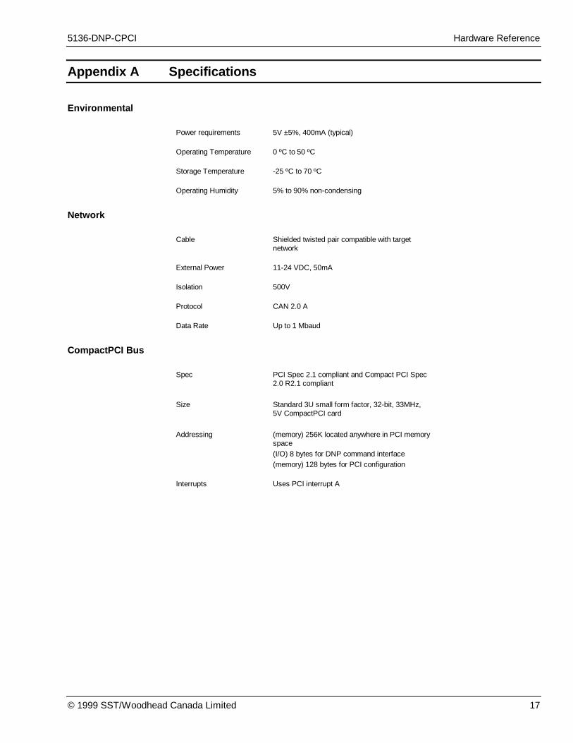
Appendix A Specifications
Environmental
Power requirements 5V ±5%, 400mA (typical)
Operating Temperature 0 ºC to 50 ºC
Storage Temperature -25 ºC to 70 ºC
Operating Humidity 5% to 90% non-condensing
Network
Cable Shielded twisted pair compatible with targetnetwork
External Power 11-24 VDC, 50mA
Isolation 500V
Protocol CAN 2.0 A
Data Rate Up to 1 Mbaud
CompactPCI Bus
Spec PCI Spec 2.1 compliant and Compact PCI Spec2.0 R2.1 compliant
Size Standard 3U small form factor, 32-bit, 33MHz,5V CompactPCI card
Addressing (memory) 256K located anywhere in PCI memoryspace(I/O) 8 bytes for DNP command interface(memory) 128 bytes for PCI configuration
Interrupts Uses PCI interrupt A
5136-DNP-CPCI Hardware Reference
© 1999 SST/Woodhead Canada Limited 18
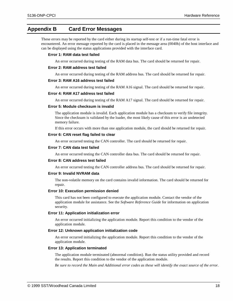
Appendix B Card Error Messages
These errors may be reported by the card either during its startup self-test or if a run-time fatal error isencountered. An error message reported by the card is placed in the message area (0040h) of the host interface andcan be displayed using the status applications provided with the interface card.
Error 1: RAM data test failed
An error occurred during testing of the RAM data bus. The card should be returned for repair.
Error 2: RAM address test failed
An error occurred during testing of the RAM address bus. The card should be returned for repair.
Error 3: RAM A16 address test failed
An error occurred during testing of the RAM A16 signal. The card should be returned for repair.
Error 4: RAM A17 address test failed
An error occurred during testing of the RAM A17 signal. The card should be returned for repair.
Error 5: Module ch ecksum is invalid
The application module is invalid. Each application module has a checksum to verify file integrity. Since the checksum is validated by the loader, the most likely cause of this error is an undetected memory failure.
If this error occurs with more than one application module, the card should be returned for repair.
Error 6: CAN reset flag failed to clear
An error occurred testing the CAN controller. The card should be returned for repair.
Error 7: CAN data test failed
An error occurred testing the CAN controller data bus. The card should be returned for repair.
Error 8: CAN address test failed
An error occurred testing the CAN controller address bus. The card should be returned for repair.
Error 9: Invalid NVRAM data
The non-volatile memory on the card contains invalid information. The card should be returned for repair.
Error 10: Execut ion p ermiss ion denied
This card has not been configured to execute the application module. Contact the vendor of the application module for assistance. See the Software Reference Guide for information on application security.
Error 11: Application initialization error
An error occurred initializing the application module. Report this condition to the vendor of the application module.
Error 12: Unknown application initialization code
An error occurred initializing the application module. Report this condition to the vendor of the application module.
Error 13: Application t erminated
The application module terminated (abnormal condition). Run the status utility provided and record the results. Report this condition to the vendor of the application module.
Be sure to record the Main and Additional error codes as these will identify the exact source of the error.
5136-DNP-CPCI Hardware Reference
© 1999 SST/Woodhead Canada Limited 19
Error 14: Application fatal error
A fatal runtime error occurred. Run the status utility provided and record the results. Report this condition to the vendor of the application module.
Be sure to record the Main and Additional error codes as these will identify the exact source of the error.
Errors 15 - 21: XXX interrupt
An unexpected interrupt was detected. This error should be reported to the vendor of the application module. Make note of the circumstances that caused this error.
Error 22: Event queue overflow
This error should be reported to the vendor of the application module. Make note of the circumstances that caused this error.
Error 23: Nested user timer interrupt
This error should be reported to the vendor of the application module. Make note of the circumstances that caused this error.
Error 24: Invalid CAN int errupt
This error should be reported to the vendor of the application module. Make note of the circumstances that caused this error.
Error 25: Nested system timer interrupt
This error should be reported to the vendor of the application module. Make note of the circumstances that caused this error.
Error 26: Imperfect interrupt
This error should be reported to the vendor of the application module. Make note of the circumstances that caused this error.
This error is caused by an incorrectly generated interrupt from the host to the card.
Error 27: Stack Overflow
This error should be reported to the vendor of the application module. Make note of the circumstances that caused this error.
Error 99: Unexpected condition encount ered
A fatal runtime error occurred. Run the status utility provided and record the results. Report this condition to the vendor of the application module.
Be sure to record the Main and Additional error codes as these will identify the exact source of the error
5136-DNP-CPCI Hardware Reference
© 1999 SST/Woodhead Canada Limited 20
Appendix C Technical Support
Before you call for help ...
Please ensure that you have the following information readily available before calling for technical support.
• Card type and serial number
• Computer’s make, model and hardware configuration (other cards installed)
• Operating system type and version
• Details of the problem you are experiencing: application module type and version, target network,circumstances that caused the problem
Getting Help
Technical support is available during regular business hours (eastern standard time) or by fax, mail, or e-mail.
Technical SupportSST, a division of Woodhead Canada Limited50 Northland RoadWaterloo, Ontario, CanadaN2V 1N3
Phone (519) 725-5136Fax (519) 725-1515
e-mail: [email protected] site: http://www.sstech.on.ca
5136-DNP-CPCI Hardware Reference
© 1999 SST/Woodhead Canada Limited 21
Appendix D Warranty
Warranty
SST warrants all new products to be free of defects in material and workmanship when applied in the manner forwhich they were intended and according to SST’s published information on proper installation. The Warrantyperiod is 1 year from the date of shipment.
SST will repair or replace, at its option, all products returned to it freight prepaid, which prove upon examinationto be within the Warranty definitions and time period.
The Warranty does not cover costs of installation, removal or damage to user's property or any contingent expensesor consequential damages. Maximum liability of SST is the cost of the product(s).
Product Returns
If it should be necessary to return or exchange items, please contact SST for a Return Authorization Code.
Inside SalesSST, a division of Woodhead Canada Limited50 Northland RoadWaterloo, Ontario, CanadaN2V 1N3
Phone (519) 725-5136Fax (519) 725-1515
e-mail: [email protected]