Embed Size (px)
Citation preview

Hard superconducting gap in InSb nanowires
Onder Gul,∗,†,‡ Hao Zhang,†,‡ Folkert K. de Vries,†,‡ Jasper van Veen,†,‡ Kun
Zuo,†,‡ Vincent Mourik,†,‡ Sonia Conesa-Boj,†,‡ Micha l P. Nowak,†,‡,¶ David J.
van Woerkom,†,‡ Marina Quintero-Perez,†,§ Maja C. Cassidy,†,‡ Attila Geresdi,†,‡
Sebastian Koelling,‖ Diana Car,†,‡,‖ Sebastien R. Plissard,‡,‖,⊥ Erik P.A.M.
Bakkers,†,‡,‖ and Leo P. Kouwenhoven∗,†,‡,#
†QuTech, Delft University of Technology, 2600 GA Delft, The Netherlands
‡Kavli Institute of Nanoscience, Delft University of Technology, 2600 GA Delft, The
Netherlands
¶Faculty of Physics and Applied Computer Science, AGH University of Science and
Technology, al. A. Mickiewicza 30, 30-059 Krakow, Poland
§Netherlands Organisation for Applied Scientific Research (TNO), 2600 AD Delft, The
Netherlands
‖Department of Applied Physics, Eindhoven University of Technology, 5600 MB
Eindhoven, The Netherlands
⊥CNRS-Laboratoire d’Analyse et d’Architecture des Systemes (LAAS), Universite de
Toulouse, 7 avenue du colonel Roche, F-31400 Toulouse, France
#Microsoft Station Q Delft, 2600 GA Delft, The Netherlands
E-mail: [email protected]; [email protected]
1
arX
iv:1
702.
0257
8v2
[co
nd-m
at.m
es-h
all]
10
Apr
201
7
Abstract
Topological superconductivity is a state of matter that can host Majorana modes,
the building blocks of a topological quantum computer. Many experimental platforms
predicted to show such a topological state rely on proximity-induced superconductivity.
However, accessing the topological properties requires an induced hard superconducting
gap, which is challenging to achieve for most material systems. We have systematically
studied how the interface between an InSb semiconductor nanowire and a NbTiN su-
perconductor affects the induced superconducting properties. Step by step, we improve
the homogeneity of the interface while ensuring a barrier-free electrical contact to the
superconductor, and obtain a hard gap in the InSb nanowire. The magnetic field sta-
bility of NbTiN allows the InSb nanowire to maintain a hard gap and a supercurrent
in the presence of magnetic fields (∼ 0.5 Tesla), a requirement for topological super-
conductivity in one-dimensional systems. Our study provides a guideline to induce
superconductivity in various experimental platforms such as semiconductor nanowires,
two dimensional electron gases and topological insulators, and holds relevance for topo-
logical superconductivity and quantum computation.
A topological superconductor can host non-Abelian excitations, the so-called Majorana
modes forming the basis of topological quantum computation.1–6 Both the non-Abelian prop-
erty and the topological protection of Majoranas crucially rely on the energy gap provided
by the superconducting pairing of electrons that separates the ground state from the higher
energy excitations. For most material systems that can support such a topological state,
pairing is artificially induced by proximity, where the host material is coupled to a supercon-
ductor in a hybrid device geometry.7–27 Accessing the topological properties in hybrid devices
requires a negligible density of states within the induced superconducting gap, i.e., an in-
duced hard gap, which can be attained by a homogeneous and barrier-free interface to the
superconductor.28–32 However, achieving such interfaces remains an outstanding challenge
for many material systems, constituting a major bottleneck for topological superconduc-
2

tivity. Here we engineer a high-quality interface between semiconducting InSb nanowires
and superconducting NbTiN resulting in an induced hard gap in the nanowire by improving
the homogeneity of the hybrid interface while ensuring a barrier-free electrical contact to
the superconductor. Our transport studies and materials characterization demonstrate that
surface cleaning dictates the structural and electronic properties of the InSb nanowires, and
determines the induced superconductivity together with the wetting of the superconductor
on the nanowire surface. We show that both the induced gap and the supercurrent in the
nanowire withstands magnetic fields (∼ 0.5 Tesla), a requirement for topological supercon-
ductivity in one-dimensional systems.
InSb nanowires have emerged as a promising platform for topological superconductiv-
ity7,10,11,15,16 owing to a large spin-orbit coupling,33,34 a large g factor,35,36 and a high mobil-
ity.36–39 These ingredients, together with a high-quality interface to a magnetic field resilient
s-wave superconductor, are necessary to maintain a finite topological gap in one dimen-
sion.4,5,40,41 The interface quality can be inferred using tunneling spectroscopy which re-
solves the induced superconducting gap for a tunnel barrier away from the interface. To
date, tunneling spectroscopy studies on proximitized InSb nanowires have reported a sig-
nificant density of states within the superconducting gap, a so-called soft gap, suggesting
an inhomogeneous interface.7,10,11,16 These subgap states destroy the topological protection
by allowing excitations with arbitrarily small energy. Soft gaps have been observed also in
other hybrid systems for cases where tunneling spectroscopy is applicable.8,12,42,43 For other
cases, interface inhomogeneity is indirectly inferred from a decreased excess current or su-
percurrent due to a deviation from Andreev transport,44 a common observation in hybrid
systems.17,18,24 A hard gap has recently been realized in epitaxial InAs-Al materials,29–32 and
in Bi2Se319 and Bi2Te3
20,21 epitaxially grown on NbSe2, where the interface inhomogeniety
can be minimized. However these studies do not provide further insight into the soft gap
problem in material systems for which either epitaxy remains a challenge or when a high
structural quality does not guarantee a barrier-free interface (e.g. due to carrier depletion).
3

Here we tackle the soft gap problem in InSb nanowire devices by focusing on the constituents
of a hybrid device realization which are crucial for the interface.
In general, realizing a hybrid device begins with surface preparation of the host material
followed by the deposition of a superconductor. In host materials with low surface electron
density or a small number of electronic subbands such as semiconductor nanowires, the
correct surface preparation is of paramount importance to ensure a barrier-free coupling to
the superconductor. Here we also adopt this procedure for our nanowires45 whose native
surface oxide forms an insulating layer that has to be removed. We describe the details of
the nanowire growth, fabrication, and measurement setup in the Supporting Information.
Figure 1a and b show a completed device with two lithographically defined superconduct-
ing electrodes having a small separation (∼ 150 nm) on an InSb nanowire. A degenerately
doped silicon substrate acts as a global back gate, tuning the carrier density in the wire. The
small electrode separation allows us to electrostatically define a tunnel barrier in the wire
section between the electrodes by applying negative gate voltages. Figure 1c and e show the
induced gaps measured by tunneling spectroscopy for two common realizations of an InSb
nanowire hybrid device. For the device in Figure 1c, a sulfur-based solution46 is used to
clean the wire surface followed by evaporation of Ti/Al with Ti the wetting layer, whereas
Figure 1e is from a device for which the wire surface is in-situ cleaned using an argon plasma
followed by sputtering of NbTiN. Figure 1d shows the conductance traces of the sulfur-Ti/Al
device indicating a hard induced gap 2∆ ∼ 0.3 meV for low gate voltages when decreased
transmission suppresses Andreev reflection. In contrast, Figure 1f demonstrates that the
argon-NbTiN device shows a soft induced gap even for the lowest gate voltages, but with a
gap 2∆ ∼ 1 meV inherited from NbTiN, a superconductor with a large gap and high critical
field. Both device realizations present a challenge towards topological protection. In the
first case, the magnetic field (∼ 0.5 T) required to drive the wire into the topological state
destroys the superconductivity of Al (Figure S1). Al can withstand such fields when it is
very thin (< 10 nm) in the field plane, however, such thin Al films contacting a nanowire
4

0.50
2
-2
0
10
Vgate (V)
dI/dV (2e2/h)
dI/dV (2e2/h)
V (m
V)V
(mV)
AV
Vgate
SiO2
Si++
I
1 μm
a
f
d
b
e
c
sulfur + Ti/Al
argon + NbTiN
-4.8-5.8 -5.3
1
0
-1
-7-8-10 -9 -2 0 2
0
0.2
0
0.2
0
0.04
V (mV)
dI/d
V (2
e2 /h) 0
0.4
-0.8 0 0.8
0
0.6
0
0.6
0
0.4
0
V (mV)
0.2
dI/d
V (2
e2 /h)
Vgate (V)
Figure 1: InSb nanowire hybrid device and induced superconducting gaps for different de-vice realizations. (a) Top-view false-color electron micrograph of a typical device consisting of an InSbnanowire (blue) with a diameter ∼ 80 nm coupled to two superconducting electrodes (yellow) with ∼ 150nm separation. (b) Schematic of the devices and the measurement setup with bias voltage V , monitoredcurrent I, and the voltage Vgate applied on back gate (Si++ substrate) that is separated from the device bya 285 nm thick SiO2 dielectric. (c), (d) Spectroscopy of a device realized using sulfur cleaning followed byevaporation of superconducting Ti/Al (5/130 nm) electrodes. T = 250 mK. Differential conductance dI/dVis plotted as a function of bias voltage V for varying gate voltages Vgate. dI/dV traces in (d) are verticalline cuts from (c) at gate voltages marked with colored bars. dI/dV is symmetric around zero bias with twoconductance peaks at V ∼ ±0.3 mV seen for all gate voltages that result from the coherence peaks in thesuperconducting density of states at the edge of the induced gap ∆. For our device geometry with two su-perconducting electrodes 2∆ ∼ 0.3 meV. For sufficiently low Vgate, where dI/dV 2e2/h at above-gap bias(V > 2∆), tunnelling is weak, which suppresses the Andreev reflection probability revealing a hard inducedgap. Larger gate voltages decrease the tunnel barrier height where increased Andreev reflection probabilityresults in finite subgap conductance. (e), (f) Spectroscopy of a device realized using argon cleaning followedby sputtering of superconducting NbTiN (90 nm) electrodes. T = 250 mK. We find 2∆ ∼ 1 meV, muchlarger than that of the Al-based InSb hybrid device shown above. dI/dV traces in (f) show an above-gapconductance comparable to those in (d). The induced gap is soft with a nonvanishing subgap conductanceeven for the weak tunnelling regime at low Vgate, indicating a deviation from Andreev transport.
5

have so far only been achieved by epitaxy.13,14,30 In the NbTiN device prepared with argon
cleaning, the subgap states render the topological properties experimentally inaccessible.
We now turn our attention to the surface of InSb nanowires prior to superconductor
deposition. To determine the effects of surface cleaning on transport, we characterized long-
channel nanowire devices with ∼ 1 µm electrode separation where the channel surface is
cleaned using different methods, along with control devices with pristine channels (details
in the Supporting Information). Figure 2 shows the measured conductance through the
nanowire as a function of gate voltage, with the traces representing an average over different
devices and the shades indicating the standard deviation. We find that the argon-cleaned
channel behaves strikingly different than sulfur-cleaned and pristine channels. First, the
argon-cleaned channel does not pinch off, showing a finite conductance even for lowest gate
voltages, indicating a deviation from a semiconducting gate response. Second, it shows a
lower transconductance ∝ dG/dVgate compared to sulfur-cleaned and pristine channels indi-
cating a low mobility. These observations are consistent with the formation of metallic In
islands on the InSb surface after argon cleaning.47 In contrast, the sulfur-cleaned channel
shows a gate response similar to the pristine channel apart from a shift of the threshold
voltage towards negative values. This behaviour indicates a surface electron accumulation
expected for III-V semiconductors treated with sulfur-based solutions.48–50 A close inspec-
tion of the cleaned channels reveals clear differences in nanowire surface morphology after
argon and sulfur cleaning (Figure 2 inset). While argon cleaning created a roughness easily
discernible under high-resolution electron microscope for different plasma parameters, we
find that sulfur cleaning, which removes ∼ 5 nm of the wire, leaves a smoother InSb surface.
TEM studies on the cleaned wire surface confirm this observation (Figure S2). Comparable
contact resistances between argon and sulfur cleaning were achievable (e.g. in Figure 1e and
f) when the argon plasma significantly etches the nanowire surface (> 15 nm), while differ-
ent plasma parameters resulting in less etching gave consistently higher contact resistances.
This indicates that a complete removal of the native oxide (∼ 3 nm) does not guarantee a
6

200 nm 200 nm
argon-cleanedchannel
sulfur-cleanedchannel
cleaned surface
50 nmcleanedsurface
uncleaned
sulfur-cleanedargon-cleaned
Vgate (V)
G (2
e2 /h)
-30 30-15 1500
2
1
Figure 2: Effects of different surface cleaning on transport properties. Gate voltage dependentconductance G of InSb nanowire devices with ∼ 1 µm electrode separation (channel length) for argon-cleaned (pink), sulfur-cleaned (orange), and uncleaned pristine (cyan) channels. T = 4 K. Traces representensemble-averaged conductance over 6 (argon-cleaned), 3 (sulfur-cleaned), and 2 (uncleaned) different devicesmeasured at bias voltage V = 10 mV, with the shades indicating the standard deviation (see the SupportingInformation for the details of averaging). Argon-cleaned channels do not pinch off, a deviation from asemiconducting gate response, and show a low transconductance ∝ dG/dVgate indicating a low mobility. Incontrast, sulfur-cleaned channels show a gate response similar to the pristine channel but with a shift of thethreshold voltage towards negative values. Insets show high-resolution electron micrographs of argon- andsulfur-cleaned channels. Argon cleaning typically rounds the otherwise hexagonal cross section of the InSbnanowire (bottom image) and leaves a rough surface (top image). A sulfur cleaning yielding comparablecontact resistances etches the InSb nanowire much less and leaves behind a smoother surface.
7

barrier-free interface to the superconductor for InSb nanowires, which could be related to
the surface depletion of InSb previously reported for a (110) surface,51 the orientation of our
nanowire facets. In the rest of the Letter we use sulfur cleaning to remove the native oxide
on the nanowire surface prior to superconductor deposition.
Next, we investigate the wetting of the superconductor on the nanowire surface. Figure
3a shows the conductance averaged over different nanowire devices realized with and without
a thin layer of NbTi (5 nm), a reactive metal deposited immediately before the NbTiN to
ensure its wetting on the wire. Inclusion of a NbTi wetting layer substantially improves
the contact resistance of the devices. Tunneling spectroscopy (Figure 3b-d) reveals the
differences in superconducting properties of the devices with and without the wetting layer.
Figure 3b shows an induced gap 2∆ ∼ 1 meV for a device with NbTi wetting layer. Low gate
voltages bring the device into the tunneling regime revealing a hard gap, shown in Figure
3c. In contrast, Figure 3d and e show that omitting the wetting layer results in no clearly
identifiable induced gap and a tunneling conductance dominated by Coulomb blockade with
irregular diamonds. Finally, to verify the importance of the wetting of the superconductor
on the wire surface we realized InSb-Al nanowire devices without a Ti wetting layer. These
devices also showed very high contact resistances, while inclusion of Ti wetting layer gave low
contact resistances and a finite supercurrent (Figure S3), in addition to a hard gap shown in
Figure 1c and d. In the Supporting Information we comprehensively discuss our observations
related to the improvement due to inclusion of a wetting layer.
The devices prepared with sulfur cleaning and NbTi/NbTiN electrodes in Figure 3 did
not show a supercurrent, a requirement for a nanowire-based topological quantum bit.52–55
We attribute the lack of a supercurrent to a residual interface barrier effective at small
bias. This could be related to the ex-situ nature of sulfur cleaning, leaving the wire surface
exposed to ambient which cannot exclude adsorbents at the interface. To improve the small
bias response of our devices we perform an additional in-situ argon cleaning of sufficiently
low-power to avoid a damage to the InSb nanowire surface. After including this low-power
8

V (m
V)
0
1.5
0
0.6
0
0.15
dI/d
V (2
e2 /h)
Vgate (V)0 10
0
2
4
6
8
0
2
-2
0
0.2
G (2
e2 /h)
2 0 2V (mV)
dI/dV (2e2/h)
2 0 2V (mV)
4.2 4 3.8 3.6Vgate (V)
Vgate (V)00.5
dI/d
V (2
e2 /h) V (m
V)
0
2
-2
1dI/dV (2e2/h) 0
0 0.3
with wetting layerwithout wetting layer
a
d
b
e
c
Figure 3: Effects of wetting layer on the transport and superconducting properties. (a) Gatevoltage dependent conductance G of InSb nanowires devices with ∼ 150 nm electrode separation realized withand without including a NbTi (5 nm) wetting layer between the nanowire and NbTiN (90 nm) electrodes.Native oxide on the nanowire surface is removed by sulfur cleaning prior to the deposition of the electrodes.Traces represent ensemble-averaged conductance over 4 (NbTi/NbTiN) and 7 (NbTiN) different devicesmeasured at a bias voltage V = 10 mV, with the shades indicating the standard deviation (see the SupportingInformation for the details of averaging). Inclusion of a NbTi wetting layer decreases the average contactresistance (including both contacts) from ∼ 100 kΩ to ∼ 1.6 kΩ (see the Supporting Information for theextraction of contact resistance). (b), (c) Spectroscopy of a device realized with NbTi/NbTiN electrodes.Differential conductance dI/dV is plotted as a function of bias voltage V for varying gate voltages Vgate.dI/dV traces in (c) are vertical line cuts from (b) at gate voltages marked with colored bars. dI/dV issymmetric in bias with two peaks at V ∼ ±1 mV seen for all gate voltages from which we find 2∆ ∼ 1 meV.For low Vgate and away from quantum dot resonances subgap conductance vanishes, revealing a hard inducedgap. Larger gate voltages decrease the tunnel barrier height, where increased Andreev reflection probabilityresults in finite subgap conductance. (d) Spectroscopy of a device realized with NbTiN electrodes withouta NbTi wetting layer. Tunneling conductance is dominated by Coulomb blockade with irregular diamonds.Induced gap cannot be clearly identified. (e) A vertical line cut from (d) at Vgate ∼ −0.08 V (indicatedby a blue bar) with a conductance similar to the middle panel in (c). dI/dV is not symmetric in bias andcoherence peaks are not visible. All data in this figure taken at T = 250 mK.
9

argon cleaning we find a high yield of devices showing a finite supercurrent measured at 250
mK (Figure S4). For another chip with 18 nanowire devices but measured at 50 mK, we
find a clear supercurrent for all devices (Figure S5) while obtaining an induced gap 2∆ ∼ 1
meV or larger (Figure S6 and S9).
Finally we study the magnetic field response of the optimized hybrid devices combining
sulfur cleaning followed by an in-situ low-power argon cleaning, and NbTi/NbTiN super-
conducting electrodes. Figure 4a and b show the differential conductance for varying gate
voltages at zero magnetic field measured at 50 mK (details in Figure S6). We find a hard gap
2∆ ∼ 1.5 meV which confirms the noninvasiveness of our low-power cleaning. The extracted
conductance suppression at small bias compared to the above-gap conductance at large bias
is ∼ 100 (Figure S7). Next, we choose a gate voltage where the device is in the tunneling
regime (orange trace in Figure 4b) and perform spectroscopy for increasing magnetic fields
along the wire axis, shown in Figure 4c. In Figure 4d we plot the conductance traces taken
at different magnetic fields showing an induced gap which remains hard up to ∼ 0.5 T (see
Figure S8 for a logarithmic plot). Increasing fields decrease the induced gap size and increase
the subgap conductance, but a gap feature can be identified up to 2 T revealing the large crit-
ical field of NbTiN. Figure 4e and f show the critical current of another device as a function
of magnetic field, measured at a large gate voltage when the nanowire is highly conducting
(details in Figure S9). We find a critical current of ∼ 40 nA at zero magnetic field which
remains finite up to greater than 1 T. The nonmonotonous magnetic-field evolution of the
critical current can be accounted for using a model which includes Zeeman effect, spin-orbit
coupling, and a realistic nanowire geometry in the few-channel, quasi-ballistic regime – the
transport regime of our devices.56
In conclusion, we have developed a method of obtaining a hard induced gap and super-
current in InSb nanowires in the presence of magnetic fields (∼ 0.5 Tesla) by combining a
noninvasive nanowire surface cleaning together with a wetting layer between the nanowire
and the NbTiN superconductor. Our results provide a guideline for inducing superconduc-
10

0.25 T0 T
0.75 T1 T
0.5 T
0 5-5 2.5-2.5
0 50-50 25-25
0
150
-150
0
-20
20
0 2.5-2.5
0 2.5-2.5
0.2
0.02
0.05
0
0
0
0.02
0.04
0.06
0
dI/d
V (2
e2 /h)
dI/d
V (2
e2 /h)
dI/dV (2e2/h)
dI/dV (2e2/h)
dV/dI (kΩ)
V (mV)
V (mV)
V (m
V)V
(mV)
Vgate (V)
B (T)
B (T) I (nA)
V (μ
V)
I (nA
)
Vgate = -0.88 V
Vgate = 20 V
0 1 2
0 1 2
-1.5 -1 -0.75-1.25
0
2.5
-2.5
0
2.5
-2.5
0
-25
25
50
0.060
0.40
200
a
fe
dc
b
0.5 1.5
0.5 1.5
Figure 4: Tunneling spectroscopy and magnetic field response of InSb nanowire hybrid deviceswith engineered interface. (a), (b) Spectroscopy of a device realized with NbTi/NbTiN electrodes usingsulfur cleaning followed by an in-situ low-power argon cleaning. Differential conductance dI/dV is plottedas a function of bias voltage V for varying gate voltages Vgate. dI/dV traces in (b) are vertical line cutsfrom (a) at gate voltages marked with colored bars. dI/dV is symmetric in bias with two peaks at V ∼ ±1.5mV seen for all gate voltages from which we find 2∆ ∼ 1.5 meV. The induced gap is hard with vanishingsubgap conductance in the tunneling regime. (c), (d) dI/dV of the same device is plotted as a function ofbias voltage V for an increasing magnetic field B along the nanowire. Gate voltage is set to Vgate = −0.88V, the same as in the middle panel in (b). dI/dV traces in (d) are vertical line cuts from (c) at magneticfields marked with colored bars. The induced gap remains hard up to ∼ 0.5 T. Increasing fields decreasethe induced gap size and increase the subgap conductance but induced superconductivity persists up to 2 Twhere dI/dV shows a gap feature with suppressed conductance at small bias and symmetrically positionedcoherence peaks. (e) Differential resistance dV /dI of an identical device is plotted as a function of biascurrent I for an increasing magnetic field B along the nanowire. Dark regions with vanishing resistanceindicate the supercurrent which remains finite up to 1 T. Gate voltage Vgate = 20 V. (f) Current-voltagetraces from (e) at magnetic fields marked with colored bars. We find a switching current of ∼ 40 nA at zeromagnetic field, which decreases to ∼ 10 nA at 0.25 T, and to ∼ 0.5 nA at 1 T. Both devices in this figurehave an electrode separation of ∼ 150 nm. Data taken at T = 50 mK.
11
tivity in semiconductor nanowires, two dimensional electron gases and topological insulators,
and hold relevance for topological superconductivity in various material systems.
Acknowledgement
We thank S. Goswami and J. Shen for stimulating discussions and critical reading of the
manuscript, and D.B. Szombati for assistance in device fabrication. This work has been
supported by the Netherlands Organisation for Scientific Research (NWO), Foundation for
Fundamental Research on Matter (FOM), European Research Council (ERC), Office of Naval
Research (ONR N00014-16-1-2270), and Microsoft Corporation Station Q.
References
(1) Read, N.; Green, D. Phys. Rev. B 2000, 61, 10267.
(2) Kitaev, A. Y. Phys.-Usp. 2001, 44, 131–136.
(3) Fu, L.; Kane, C. L. Phys. Rev. Lett. 2008, 100, 096407.
(4) Oreg, Y.; Refael, G.; von Oppen, F. Phys. Rev. Lett. 2010, 105, 177002.
(5) Lutchyn, R. M.; Sau, J. D.; Sarma, S. D. Phys. Rev. Lett. 2010, 105, 077001.
(6) Alicea, J.; Oreg, Y.; Refael, G.; von Oppen, F.; Fisher, M. P. Nat. Phys. 2011, 7,
412–417.
(7) Mourik, V.; Zuo, K.; Frolov, S. M.; Plissard, S.; Bakkers, E.; Kouwenhoven, L. Science
2012, 336, 1003–1007.
(8) Das, A.; Ronen, Y.; Most, Y.; Oreg, Y.; Heiblum, M.; Shtrikman, H. Nat. Phys. 2012,
8, 887–895.
(9) Rokhinson, L. P.; Liu, X.; Furdyna, J. K. Nat. Phys. 2012, 8, 795–799.
12

(10) Deng, M. T.; Yu, C. L.; Huang, G. Y.; Larsson, M.; Caroff, P.; Xu, H. Q. Nano Lett.
2012, 12, 6414–6419.
(11) Churchill, H. O. H.; Fatemi, V.; Grove-Rasmussen, K.; Deng, M. T.; Caroff, P.;
Xu, H. Q.; Marcus, C. M. Phys. Rev. B 2013, 87, 241401.
(12) Finck, A. D. K.; Van Harlingen, D. J.; Mohseni, P. K.; Jung, K.; Li, X. Phys. Rev. Lett.
2013, 110, 126406.
(13) Albrecht, S.; Higginbotham, A.; Madsen, M.; Kuemmeth, F.; Jespersen, T.; Nygard, J.;
Krogstrup, P.; Marcus, C. Nature 2016, 531, 206–209.
(14) Deng, M. T.; Vaitiekenas, S.; Hansen, E. B.; Danon, J.; Leijnse, M.; Flensberg, K.;
Nygard, J.; Krogstrup, P.; Marcus, C. M. Science 2016, 354, 1557–1562.
(15) Zhang, H.; Gul, O.; Conesa-Boj, S.; Zuo, K.; Mourik, V.; de Vries, F. K.; van Veen, J.;
van Woerkom, D. J.; Nowak, M. P.; Wimmer, M. et al. 2016, arXiv:1603.04069.
(16) Chen, J.; Yu, P.; Stenger, J.; Hocevar, M.; Car, D.; Plissard, S. R.; Bakkers, E. P.
A. M.; Stanescu, T. D.; Frolov, S. M. 2016, arXiv:1610.04555.
(17) Hart, S.; Ren, H.; Wagner, T.; Leubner, P.; Muhlbauer, M.; Brune, C.; Buhmann, H.;
Molenkamp, L. W.; Yacoby, A. Nat. Phys. 2014, 10, 638–643.
(18) Pribiag, V. S.; Beukman, A. J.; Qu, F.; Cassidy, M. C.; Charpentier, C.; Wegschei-
der, W.; Kouwenhoven, L. P. Nat. Nanotechnol. 2015, 10, 593–597.
(19) Wang, M.-X.; Liu, C.; Xu, J.-P.; Yang, F.; Miao, L.; Yao, M.-Y.; Gao, C. L.; Shen, C.;
Ma, X.; Chen, X. et al. Science 2012, 336, 52–55.
(20) Xu, J.-P.; Liu, C.; Wang, M.-X.; Ge, J.; Liu, Z.-L.; Yang, X.; Chen, Y.; Liu, Y.;
Xu, Z.-A.; Gao, C.-L. et al. Phys. Rev. Lett. 2014, 112, 217001.
13

(21) Xu, J.-P.; Wang, M.-X.; Liu, Z. L.; Ge, J.-F.; Yang, X.; Liu, C.; Xu, Z. A.; Guan, D.;
Gao, C. L.; Qian, D. et al. Phys. Rev. Lett. 2015, 114, 017001.
(22) Williams, J. R.; Bestwick, A. J.; Gallagher, P.; Hong, S. S.; Cui, Y.; Bleich, A. S.;
Analytis, J. G.; Fisher, I. R.; Goldhaber-Gordon, D. Phys. Rev. Lett. 2012, 109, 056803.
(23) Wiedenmann, J.; Bocquillon, E.; Deacon, R. S.; Hartinger, S.; Herrmann, O.; Klap-
wijk, T. M.; Maier, L.; Ames, C.; Brune, C.; Gould, C. et al. Nat. Commun. 2016, 7,
10303.
(24) Bocquillon, E.; Deacon, R. S.; Wiedenmann, J.; Leubner, P.; Klapwijk, T. M.;
Brune, C.; Ishibashi, K.; Buhmann, H.; Molenkamp, L. W. Nat. Nanotechnol. 2017,
12, 137–143.
(25) Wan, Z.; Kazakov, A.; Manfra, M. J.; Pfeiffer, L. N.; West, K. W.; Rokhinson, L. P.
Nat. Commun. 2015, 6, 7426.
(26) Pientka, F.; Keselman, A.; Berg, E.; Yacoby, A.; Stern, A.; Halperin, B. I. 2016,
arXiv:1609.09482.
(27) Hell, M.; Leijnse, M.; Flensberg, K. Phys. Rev. Lett. 2017, 118, 107701.
(28) Takei, S.; Fregoso, B. M.; Hui, H.-Y.; Lobos, A. M.; Sarma, S. D. Phys. Rev. Lett.
2013, 110, 186803.
(29) Chang, W.; Albrecht, S.; Jespersen, T.; Kuemmeth, F.; Krogstrup, P.; Nygard, J.;
Marcus, C. Nat. Nanotechnol. 2015, 10, 232–236.
(30) Krogstrup, P.; Ziino, N.; Chang, W.; Albrecht, S.; Madsen, M.; Johnson, E.; Nygard, J.;
Marcus, C.; Jespersen, T. Nat. Mater. 2015, 14, 400–406.
(31) Kjaergaard, M.; Nichele, F.; Suominen, H.; Nowak, M.; Wimmer, M.; Akhmerov, A.;
Folk, J.; Flensberg, K.; Shabani, J.; Palmstrøm, C. et al. Nat. Commun. 2016, 7,
12841.
14

(32) Shabani, J.; Kjaergaard, M.; Suominen, H. J.; Kim, Y.; Nichele, F.; Pakrouski, K.;
Stankevic, T.; Lutchyn, R. M.; Krogstrup, P.; Feidenhans’l, R. et al. Phys. Rev. B
2016, 93, 155402.
(33) van Weperen, I.; Tarasinski, B.; Eeltink, D.; Pribiag, V. S.; Plissard, S. R.; Bakkers, E.
P. A. M.; Kouwenhoven, L. P.; Wimmer, M. Phys. Rev. B 2015, 91, 201413.
(34) Kammhuber, J.; Cassidy, M. C.; Pei, F.; Nowak, M. P.; Vuik, A.; Car, D.; Plis-
sard, S. R.; Bakkers, E. P. A. M.; Wimmer, M.; Kouwenhoven, L. P. 2017,
arXiv:1701.06878.
(35) van Weperen, I.; Plissard, S. R.; Bakkers, E. P. A. M.; Frolov, S. M.; Kouwenhoven, L. P.
Nano Lett. 2012, 13, 387–391.
(36) Kammhuber, J.; Cassidy, M. C.; Zhang, H.; Gul, O.; Pei, F.; de Moor, M. W. A.;
Nijholt, B.; Watanabe, K.; Taniguchi, T.; Car, D. et al. Nano Lett. 2016, 16, 3482–
3486.
(37) Gul, O.; van Woerkom, D. J.; van Weperen, I.; Car, D.; Plissard, S. R.; Bakkers, E. P.
A. M.; Kouwenhoven, L. P. Nanotechnology 2015, 26, 215202.
(38) Li, S.; Kang, N.; Fan, D.; Wang, L.; Huang, Y.; Caroff, P.; Xu, H. Sci. Rep. 2016, 6,
24822.
(39) Gill, S.; Damasco, J.; Car, D.; Bakkers, E. P. A. M.; Mason, N. Appl. Phys. Lett. 2016,
109, 233502.
(40) Potter, A. C.; Lee, P. A. Phys. Rev. B 2011, 83, 184520.
(41) Sau, J. D.; Tewari, S.; Sarma, S. D. Phys. Rev. B 2012, 85, 064512.
(42) Irie, H.; Todt, C.; Kumada, N.; Harada, Y.; Sugiyama, H.; Akazaki, T.; Muraki, K.
Phys. Rev. B 2016, 94, 155305.
15
(43) Su, Z.; Zarassi, A.; Nguyen, B.-M.; Yoo, J.; Dayeh, S. A.; Frolov, S. M. 2016,
arXiv:1610.03010.
(44) Blonder, G.; Tinkham, M.; Klapwijk, T. Phys. Rev. B 1982, 25, 4515.
(45) Car, D.; Wang, J.; Verheijen, M. A.; Bakkers, E. P. A. M.; Plissard, S. R. Adv. Mater.
2014, 26, 4875–4879.
(46) Suyatin, D.; Thelander, C.; Bjork, M.; Maximov, I.; Samuelson, L. Nanotechnology
2007, 18, 105307.
(47) Bouslama, M.; Jardin, C.; Ghamnia, M. Vacuum 1995, 46, 143–146.
(48) King, P.; Veal, T. D.; Lowe, M. J.; McConville, C. F. J. Appl. Phys. 2008, 104, 083709.
(49) Petrovykh, D.; Yang, M.; Whitman, L. Surf. Sci. 2003, 523, 231–240.
(50) Ho, J. C.; Ford, A. C.; Chueh, Y.-L.; Leu, P. W.; Ergen, O.; Takei, K.; Smith, G.;
Majhi, P.; Bennett, J.; Javey, A. Appl. Phys. Lett. 2009, 95, 072108.
(51) Gobeli, G.; Allen, F. Phys. Rev. 1965, 137, A245.
(52) Hyart, T.; van Heck, B.; Fulga, I.; Burrello, M.; Akhmerov, A.; Beenakker, C. Phys.
Rev. B 2013, 88, 035121.
(53) Plugge, S.; Rasmussen, A.; Egger, R.; Flensberg, K. New J. Phys. 2017, 19, 012001.
(54) Vijay, S.; Fu, L. Phys. Rev. B 2016, 94, 235446.
(55) Karzig, T.; Knapp, C.; Lutchyn, R.; Bonderson, P.; Hastings, M.; Nayak, C.; Alicea, J.;
Flensberg, K.; Plugge, S.; Oreg, Y. et al. 2016, arXiv:1610.05289.
(56) Zuo, K.; Mourik, V.; Szombati, D. B.; Nijholt, B.; van Woerkom, D. J.; Geresdi, A.;
Chen, J.; Ostroukh, V. P.; Akhmerov, A. R.; Plissard, S. R. et al. in preparation.
16
Supporting Information: Hard superconducting gap in InSb
nanowires
Onder Gul1,2,∗, Hao Zhang1,2, Folkert K. de Vries1,2, Jasper van Veen1,2, Kun Zuo1,2,
Vincent Mourik1,2, Sonia Conesa-Boj1,2, Micha l P. Nowak1,2,3, David J. van Woerkom1,2,
Marina Quintero-Perez1,4, Maja C. Cassidy1,2, Attila Geresdi1,2, Sebastian Koelling5,
Diana Car1,2,5, Sebastien R. Plissard2,5,6, Erik P.A.M. Bakkers1,2,5,
Leo P. Kouwenhoven1,2,7,†
1QuTech, Delft University of Technology, 2600 GA Delft, The Netherlands2Kavli Institute of Nanoscience, Delft University of Technology, 2600 GA Delft, The Netherlands3Faculty of Physics and Applied Computer Science, AGH University of Science and Technology,
al. A. Mickiewicza 30, 30-059 Krakow, Poland4Netherlands Organisation for Applied Scientific Research (TNO), 2600 AD Delft, The
Netherlands5Department of Applied Physics, Eindhoven University of Technology, 5600 MB Eindhoven, The
Netherlands6CNRS-Laboratoire d’Analyse et d’Architecture des Systemes (LAAS), Universite de Toulouse, 7
avenue du colonel Roche, F-31400 Toulouse, France7Microsoft Station Q Delft, 2600 GA Delft, The Netherlands
∗E-mail: [email protected] †E-mail: [email protected]
Author contributions. OG, FKdV, KZ, and VM developed the noninvasive surface cleaning and
the inclusion of wetting layer. OG, HZ, and JvV optimized the noninvasive surface cleaning. SCB
did the TEM analysis. MPN did the theoretical analysis. DJvW contributed to device fabrication.
MQP and MCC optimized the NbTiN films. AG contributed to the data analysis. SK prepared
the lamellae for TEM analysis. DC, SRP, and EPAMB grew the InSb nanowires. OG wrote the
manuscript with contributions from all authors. LPK supervised the project.
17
List of supporting text and figures
Nanowire growth and device fabrication
Fabrication details of the long-channel devices in Figure 2
Measurement setup
Details of ensemble averaging
Extraction of contact resistance
Discussion of the wetting layer
Figure S1: Magnetic field response of the induced gap in InSb nanowire hybrid
device with Ti/Al electrodes
Figure S2: Cross-sectional transmission electron micrographs of the nanowire
surface cleaned using different methods
Figure S3: Additional transport properties of InSb nanowire hybrid devices with
Ti/Al electrodes
Figure S4: Supercurrent in InSb nanowire hybrid devices with NbTi/NbTiN
electrodes
Figure S5: Supercurrent in InSb nanowire hybrid devices with NbTi/NbTiN
electrodes at T = 50 mK
Figure S6: Additional transport properties of InSb nanowire hybrid device with
engineered interface (device A)
Figure S7: Figure 4b replotted in logarithmic conductance scale
Figure S8: Figure 4d replotted in logarithmic conductance scale
Figure S9: Additional transport properties of InSb nanowire hybrid device with
engineered interface (device B)
18

Nanowire growth and device fabrication. InSb nanowires have been grown by Au-
catalyzed Vapor-Liquid-Solid mechanism in a Metal Organic Vapor Phase Epitaxy reactor.
The InSb nanowire crystal direction is [111] zinc blende, free of stacking faults and dis-
locations.1 Nanowires are deposited one-by-one using a micro-manipulator2 on a p-Si++
substrate covered with 285 nm thick SiO2 serving as a dielectric for back gate. Superconduc-
tor deposition process starts with resist development followed by oxygen plasma cleaning.
For sulfur cleaning, the chip is immersed in a Sulfur-rich ammonium sulfide solution diluted
by water (with a ratio of 1:200) at 60C for half an hour.3 At all stages care is taken to ex-
pose the solution to air as little as possible. Ti/Al contacts are e-beam evaporated at a base
pressure < 10−7 mbar. In-situ argon plasma cleaning and NbTiN deposition is performed in
an AJA International ATC 1800 sputtering system with a base pressure ∼ 10−9 Torr. For
devices without sulfur cleaning, argon cleaning is performed using an argon plasma typically
at a pressure of 3 mTorr and a power of 100 Watts applied for 150 seconds, but different
plasma parameters removing a similar thickness of InSb from the nanowire surface (> 15
nm) gave similar transport properties. For devices with sulfur cleaning we used a much
milder argon plasma at a pressure of 10 mTorr and a power of 25 Watts applied for ∼ 5
seconds. For NbTiN deposition a Nb0.7Ti0.3 wt. % target with a diameter of 3 inches is used.
Reactive sputtering resulting in (NbTi) NbTiN films was performed in an Ar/N process gas
with (0) 8.3 at. % nitrogen content at a pressure of 2.5 mTorr using a dc magnetron sputter
source at a power of 250 Watts. An independent characterization of the NbTiN films gave
a critical temperature of 13.5 K for 90 nm thick films with a resistivity of 114 µΩ·cm and a
compressive stress on Si substrate.
Fabrication details of the long-channel devices in Figure 2. For the InSb nanowire
devices with sulfur-cleaned channels, the cleaning of the channel is performed after a complete
fabrication of the electrodes contacting the nanowire. For the devices whose transport data
is presented, sulfur cleaning is applied to the entire channel, while the inset shows a partially
cleaned channel to illustrate the mild etching of the wire. For the nanowire devices with
argon-cleaned channels, the cleaning of the channel is performed before the fabrication of the
contact electrodes. However, we obtained a similar result when argon cleaning was applied
after fabricating the contacts. For all long-channel devices we used argon cleaning to remove
the native oxide on the nanowire surface prior to contact deposition.
Measurement setup. All the data in this study is measured using RC, copper powder,
and π filters thermalized at different temperatures. Differential conductance measurements
are performed using standard ac lock-in techniques. Nanowire devices are kept in vacuum
during low temperature measurements.
Details of ensemble averaging. Conductance is averaged over different nanowire devices
19
for each value of gate voltage. Devices within an ensemble are fabricated simultaneously on
a single substrate, have identical geometries, and are measured during the same cool down.
Extraction of contact resistance. We extract contact resistances by fitting the conduc-
tance measured as a function of gate voltage using the method described in Ref. S4. Here
we leave the product of capacitance and mobility as a free fit parameter which is not taken
into consideration.
Discussion of the wetting layer. Throughout our study we have tried various etching
techniques (HF, lactic acid, sulfur solution, He ion beam, Ar plasma) in combination with dif-
ferent contact materials (Ti, Al, V, Cr - evaporation; Al, NbTi, NbTiN, MoRe - sputtering).
Our observations rule out a work function (W ) related explanation for the improvement due
to inclusion of a wetting layer: Ti (W = 4.33 eV)5 and Cr (W = 4.5 eV)5 gives significantly
lower contact resistances on our wires than Al (W = 4.06 – 4.26 eV)5 – known for its low
work function. (See Ref. S6 for Cr/Au contacts on our wires.) Consistent observation of
the improvement due to wetting layer both for evaporation (Al) and for reactive sputtering
(NbTiN) suggests that the mechanism of improvement is independent of the details of the
deposition environment, such as nitrogen plasma. We further note that sputtered Al contacts
also result in low contact transparency with large contact resistances (no difference observed
between evaporated and sputtered Al contacts without a wetting layer). Finally, a Ti wetting
layer provides improvement for Al contacts on InAs nanowires as well7 – consistent with our
observations. However, it is possible to realize transparent contacts of Al on InAs when the
Al-InAs interface is homogeneous (epitaxial).7 This suggests that the nucleation of the Al
film deposited on the wire is a key factor which determines the transparency.
20
B (mT)
V (m
V)dI/dV (2e2/h)
0
-0.520 40
0.50.50
0
Figure S1: Magnetic field response of the induced gap in InSb nanowire hybrid
device with Ti/Al electrodes. Differential conductance dI/dV is plotted as a function of
bias voltage V for increasing magnetic fieldB along the nanowire axis. The nanowire device is
in the tunneling regime with dI/dV 2e2/h for above-gap bias (V > 2∆). At zero magnetic
field dI/dV shows two conductance peaks at V ∼ ±0.3 mV symmetric around zero bias
giving 2∆ ∼ 0.3 meV. Increasing the magnetic field decreases the size of the superconducting
gap ∆ which completely vanishes at ∼ 25 mT. The device shows no superconductivity at
larger magnetic fields. Device realized by sulfur cleaning. Ti/Al electrodes have a thickness
of 5/130 nm and a separation of ∼ 150 nm on the nanowire. T = 50 mK.
21

a b
InSb
substrate
InSb20 nm 20 nm
cleanedsurface
cleanedsurface
Figure S2: Cross-sectional transmission electron micrographs of the nanowire sur-
face cleaned using different methods. The cuts were performed along the nanowire
axis. (a) InSb nanowire surface after argon plasma cleaning. Argon cleaning leaves a rough
nanowire surface. Nanowire appears thinner due to substantial etching. (b) InSb nanowire
surface after sulfur cleaning followed by a low-power argon cleaning (see main text for de-
tails). Sulfur cleaning leaves a smoother nanowire surface.
22

-10 0 100
2
4
6
10
G(2
e2 /h)
Vgate (V)
8
-10 0 10-25
0
25
V (µ
V)
I (nA)
Figure S3: Additional transport properties of InSb nanowire hybrid devices with
Ti/Al electrodes. Conductance G of InSb nanowire devices is plotted as a function of gate
voltage Vgate. The trace represents ensemble-averaged conductance over 6 different devices
on a single chip and the shade indicates the standard deviation. Taken at a bias voltage
V = 10 mV. Average contact resistance (including both contacts) is ∼ 1 kΩ. Inset shows
voltage drop V as a function of bias current I for one of the 6 devices. We find a clear
supercurrent up to ∼ 10 nA. Red trace shows the current-voltage response when the bias
current is swept in positive direction, black trace the negative direction. Gate voltage is set
to Vgate = 9 V. Ti/Al electrodes have a thickness of 5/130 nm and a separation of ∼ 150 nm
on the nanowire. All data in this figure taken at T = 250 mK.
23
-20 -10 0 10 20 30
-0.1
0.0
0.1
V (m
V)
I (nA)
device 1 device 2 device 4device 5device 6
device 3
Figure S4: Supercurrent in InSb nanowire hybrid devices with NbTi/NbTiN elec-
trodes. Devices realized using sulfur cleaning followed by an in-situ low-power argon clean-
ing. T = 250 mK. Voltage drop V is plotted as a function of bias current I for different
devices on a single chip with 8 devices in total. An in-situ low-power argon cleaning improves
the small bias response allowing to resolve a supercurrent for a high yield of devices. Gate
voltage is set to Vgate = 18 V. NbTi/NbTiN electrodes have a thickness of 5/90 nm and a
separation of ∼ 150 nm on the nanowire.
24

-40 -20 0 20 40
0
-40 -20 0 20 40
0
-40 -20 0 20 40
0
-40 -20 0 20 40
0
-40 -20 0 20 40
0
-40 -20 0 20 40
0
-0.1
0.1
-0.1
0.1
-0.1
0.1
-0.1
0.1
-0.2
0.2
-0.1
0.1
I (nA)
V (m
V)V
(mV)
V (m
V)V
(mV)
V (m
V)V
(mV)
-40 -20 0 20 40
0
-40 -20 0 20 40
0
-50 -25 0 25 50
0
-40 -20 0 20 40
0
-40 -20 0 20 40
0
-40 -20 0 20 40
0
-0.2
0.2
-0.2
0.2
-0.1
0.1
-0.1
0.1
-0.2
0.2
-0.1
0.1
I (nA)
device B
0
-40 -20 0 20 40
0
-40 -20 0 20 40
0
-40 -20 0 20 40
0
-40 -20 0 20 40
-40 -20 0 20 40
0
-40 -20 0 20 40
0
-0.1
0.1
-0.1
0.1
-0.1
0.1
-0.1
0.1
-0.3
0.3
-0.05
0.05
I (nA)
device A
Figure S5: Supercurrent in InSb nanowire hybrid devices with NbTi/NbTiN elec-
trodes at T = 50 mK. Devices realized using sulfur cleaning followed by an in-situ low-
power argon cleaning. Voltage drop V is plotted as a function of bias current I for all
devices on a single chip. We find a clear supercurrent in every device. Red traces show the
current-voltage response when the bias current is swept in positive direction, black traces the
negative direction. We relate the origin of the hysteresis to electron heating.8 Gate voltage
is set to Vgate = 20 V. NbTi/NbTiN electrodes have a thickness of 5/90 nm and a separation
of ∼ 150 nm on the nanowire. Data in Figure 4a-d is taken from Device A, data in Figure
4e,f taken from Device B.
25

2.5
device A
Vgate (V)
V (m
V)
-2.5
0
dI/dV (2e2/h)
0
1
2
3
Vgate = 0.315 V
G (2
e2 /h)
Vgate (V)
experimentfit
V (mV)Vgate (V)
Tran
smis
sion
I (nA
)
-1 -0.5 0 0.5 0 1 2
50
100
0
1
0.5
00 10 20
a b
c d
Figure S6: Additional transport properties of InSb nanowire hybrid device with
engineered interface (device A). All data in this figure is taken from device A, the device
in Figure 4a-d. (a) Conductance G of InSb nanowire device is plotted as a function of gate
voltage Vgate, taken at a bias voltage V = 10 mV. Extracted contact resistance (including
both contacts) ∼ 1.6 kΩ. (b) Differential conductance dI/dV is plotted as a function of
bias voltage V for a large gate voltage Vgate range. (c) Transmission T extracted from (b)
by fitting the measured current I using Averin-Bardas model.9,10 Best fit is obtained for a
single channel transport through the nanowire. Transmission reaches ∼ 0.9 giving a lower
bound on contact transparency assuming a single channel transport. We note that our model
does not account for the observed finite contact transparencies and conductance resonances,
decreasing the certainty of our estimate. (d) The measured current I and the corresponding
fit is plotted for Vgate = 0.315 V.
26

V (mV)0-3 -1.5 31.5
1
10-2
10-3
10-4
10-5
dI/d
V (2
e2 /h)
10-1
-0.75-0.88-1.02
Vgate (V)
Figure S7: Figure 4b replotted in logarithmic conductance scale. Differential con-
ductance dI/dV is plotted as a function of bias voltage V for varying gate voltages Vgate. The
extracted conductance suppression at small bias compared to the above-gap conductance at
large bias is ∼ 100.
27

00.51
B (T)
V (mV)0-3 -1.5 31.5
10-1
10-2
10-3
10-4
10-5
dI/d
V (2
e2 /h)
Figure S8: Figure 4d replotted in logarithmic conductance scale. Differential con-
ductance dI/dV is plotted as a function of bias voltage V for varying magnetic fields B
along the wire axis. The induced gap remains hard up to ∼ 0.5 T.
28
G (2
e2 /h)
Vgate (V)
a
B (T)
4
3
2
1
00 20 0 1.50.5 2110
-2.5
0
2.5dI/dV (2e2/h)
V (m
V)
device B
c 0 0.5
2.5
Vgate (V)
-2.5
V (m
V)
dI/dV (2e2/h)0 1
device B
b
0
0 1.50.5 1
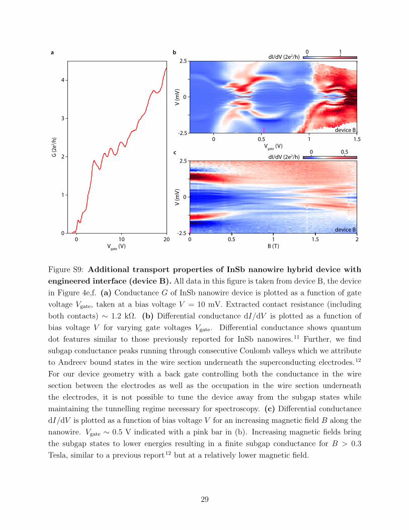
Figure S9: Additional transport properties of InSb nanowire hybrid device with
engineered interface (device B). All data in this figure is taken from device B, the device
in Figure 4e,f. (a) Conductance G of InSb nanowire device is plotted as a function of gate
voltage Vgate, taken at a bias voltage V = 10 mV. Extracted contact resistance (including
both contacts) ∼ 1.2 kΩ. (b) Differential conductance dI/dV is plotted as a function of
bias voltage V for varying gate voltages Vgate. Differential conductance shows quantum
dot features similar to those previously reported for InSb nanowires.11 Further, we find
subgap conductance peaks running through consecutive Coulomb valleys which we attribute
to Andreev bound states in the wire section underneath the superconducting electrodes.12
For our device geometry with a back gate controlling both the conductance in the wire
section between the electrodes as well as the occupation in the wire section underneath
the electrodes, it is not possible to tune the device away from the subgap states while
maintaining the tunnelling regime necessary for spectroscopy. (c) Differential conductance
dI/dV is plotted as a function of bias voltage V for an increasing magnetic field B along the
nanowire. Vgate ∼ 0.5 V indicated with a pink bar in (b). Increasing magnetic fields bring
the subgap states to lower energies resulting in a finite subgap conductance for B > 0.3
Tesla, similar to a previous report12 but at a relatively lower magnetic field.
29

References
(S1) Car, D.; Wang, J.; Verheijen, M. A.; Bakkers, E. P. A. M.; Plissard, S. R. Adv. Mater.
2014, 26, 4875.
(S2) Flohr, K.; Liebmann, M.; Sladek, K.; Gunel, H. Y.; Frielinghaus, R.; Haas, F.; Meyer,
C.; Hardtdegen, H.; Schapers, T.; Grutzmacher, D. et al. Rev. Sci. Instrum. 2011,
82, 113705.
(S3) Suyatin, D.; Thelander, C.; Bjork, M.; Maximov, I.; Samuelson, L. Nanotechnology
2007, 18, 105307.
(S4) Gul, O.; van Woerkom, D. J.; van Weperen, I.; Car, D.; Plissard, S. R.; Bakkers, E.
P. A. M.; Kouwenhoven, L. P. Nanotechnology 2015, 26, 215202.
(S5) Haynes, W. M. (ed.) CRC Handbook of Chemistry and Physics, 2017, 97th Edition
(Internet Version), CRC Press/Taylor & Francis.
(S6) Kammhuber, J.; Cassidy, M. C.; Zhang, H.; Gul, O.; Pei, F.; de Moor, M. W. A.;
Nijholt, B.; Watanabe, K.; Taniguchi, T.; Car, D. et al. Nano Lett. 2016, 16, 3482.
(S7) Chang, W.; Albrecht, S.; Jespersen, T.; Kuemmeth, F.; Krogstrup, P.; Nygard, J.;
Marcus, C. Nat. Nanotechnol. 2015, 10, 232.
(S8) Courtois, H.; Meschke, M.; Peltonen, J. T.; Pekola, J. P. Phys. Rev. Lett. 2008, 101,
067002.
(S9) Averin, D.; Bardas, A. Phys. Rev. Lett. 1995, 75, 1831.
(S10) Kjaergaard, M.; Suominen, H. J.; Nowak, M. P.; Akhmerov, A. R.; Shabani, J.;
Palmstrøm, C. J.; Nichele, F.; Marcus, C. M. 2016, arXiv:1607.04164.
(S11) Li, S.; Kang, N.; Caroff, P.; Xu, H. Q. Phys. Rev. B 2017, 95, 014515.
(S12) Deng, M. T.; Vaitiekenas, S.; Hansen, E. B.; Danon, J.; Leijnse, M.; Flensberg, K.;
Nygard, J.; Krogstrup, P.; Marcus, C. M. Science 2016, 354, 1557.
30


![Strained -Sn on InSb(001) · InSb, is likewise a heteroepitaxial strained system. The use of InSb as a template for high quality crystals is well established [18{20]. It induces a](https://img.dokumen.tips/doc/110x75/5f63835e50764f10ad37eb67/strained-sn-on-insb001-insb-is-likewise-a-heteroepitaxial-strained-system-the.jpg)


![InSb, ) InAsSb InSb. II 32advance.orion-ir.ru/UPF-17/3/UPF-5-3-271.pdfного» InSb, ЭС InSb, ЭС InAsSb и nBn-бариода на InAsSb [23]. В области низких](https://img.dokumen.tips/doc/110x75/5f63839e4bcb9c59cf1945e8/insb-inassb-insb-ii-insb-insb-inassb-nbn-.jpg)