Embed Size (px)
Citation preview

Growth, Structure, and Electronic Properties of Epitaxial BismuthTelluride Topological Insulator Films on BaF2 (111) SubstratesO. Caha,† A. Dubroka,† J. Humlícek,† V. Holy,‡ H. Steiner,§ M. Ul-Hassan,§ J. Sanchez-Barriga,∥
O. Rader,∥ T. N. Stanislavchuk,⊥ A. A. Sirenko,⊥ G. Bauer,§ and G. Springholz*,§
†Department of Condensed Matter Physics and CEITEC, Masaryk University, Kotlarska 2, 61137 Brno, Czech Republic‡Department of Electronic Structures, Charles University, Praha, Czech Republic§Institut fur Halbleiter- und Festkorperphysik, Johannes Kepler Universitat, Altenbergerstrasse 69, 4040 Linz, Austria∥Helmholtz-Zentrum Berlin fur Materialien und Energie, Elektronenspeicherring BESSY II, Albert-Einstein-Straße 15, 12489 Berlin,Germany⊥Department of Physics, New Jersey Institute of Technology, Newark, New Jersey 07102, United States
*S Supporting Information
ABSTRACT: Epitaxial growth of topological insulatorbismuth telluride by molecular beam epitaxy onto BaF2(111) substrates is studied using Bi2Te3 and Te as sourcematerials. By changing the beam flux composition, differentstoichiometric phases are obtained, resulting in high qualityBi2Te3 and Bi1Te1 epilayers as shown by Raman spectroscopyand high-resolution X-ray diffraction. From X-ray reciprocalspace mapping, the residual strain, as well as size of coherentlyscattering domains are deduced. The Raman modes for thetwo different phases are identified and the dielectric functionsderived from spectroscopic ellipsometry investigations.Angular resolved photoemission reveals topologically pro-tected surface states of the Bi2Te3 epilayers. Thus, BaF2 is aperfectly suited substrate material for the bismuth telluride compounds.
■ INTRODUCTION
Recent discovery of a new class of materials, called topologicalinsulators, has opened up a whole new research arena.1−5
Topological insulators behave in the bulk like ordinaryinsulators but support in addition a conducting two-dimen-sional topological surface state with linear energy-momentumdispersion shaped like a Dirac cone.2,6,7 Because of strongspin−orbit coupling, the electron momentum in these surfacestates is locked to the spin orientation and spin-flip scattering isprohibited by time reversal symmetry.1,8 As a result, spinpolarized currents can be produced without the needs ofexternal magnetic fields, which offers great advantages forspintronic or quantum computation applications.1,5,9 Thehelical spin structure of the topological surface states alsoprovides a basis for fundamental new physics such as magneticmonopoles and Majorana fermions.1,2
Among the new materials exhibiting three-dimensionaltopological insulating properties, the bismuth chalcogenidesBi2Te3 and Bi2Se3 have attracted most attention because asingle Dirac cone is formed at the Γ-point of the Brillouin zonewithin the bulk band gap, as has been revealed by angularresolved photoemission6,7 and scanning tunneling spectroscopystudies.10,11 Bi2Te3 is also a superior thermoelectric material forenergy harvesting applications, since it exhibits the highest
thermoelectric figure of merit at room temperature among allbulk materials.12,13 Up to now, most studies of the topologicalproperties of Bi2Te3 have been performed on bulk singlecrystals cleaved under ultrahigh vacuum conditions.3,7,14 Forpractical device applications, however, epitaxial layers aredesired15 for monolithic integration in multilayers and gatedheterostructures that would allow tuning of the Fermi level tothe Dirac point and control spin polarized currents indevices.15,16 Considerable efforts have been made to growBi2Te3 epitaxially on substrates like Si17−21 or GaAs,22−26
which, however, exhibit a very large lattice mismatch of up to14% to Bi2Te3.Bismuth telluride can crystallize in several different crystal
structures in dependence of its stoichiometric composition. Thecrystal structure of the most common Bi2Te3 phase consists ofof three Te1−Bi−Te2−Bi−Te1 quintuplet layers (QL) asfundamental building block (see Figure 1a). These are stackedon top of each other in an ABCABC stacking sequence. Inaddition, several alternative phases with lower Te concentrationexist, including Bi1Te1 (called tsumoite), as well as Bi3Te4 and
Received: January 9, 2013Revised: May 15, 2013Published: July 12, 2013
Article
pubs.acs.org/crystal
© 2013 American Chemical Society 3365 dx.doi.org/10.1021/cg400048g | Cryst. Growth Des. 2013, 13, 3365−3373

Bi4Te3 (pilsenite) among others.27 The different phases sharethe same hexagonal structure of R3m space group symmetry,but show a different stacking of the Bi and Te layers.28,29 TheBi1Te1 structure, depicted in Figure 1b, consists of twelveatomic Te1−Bi1−Te2−Bi2−Te3−Bi3−Bi3−Te3−Bi2−Te2−Bi1−Te1 lattice planes30 that can be split into two mirrored hextuplelayers (HL). The unit cells of Bi4Te3 and Bi3Te4 consist even of21 lattice planes grouped in three blocks of septuplet layers,comprising each of seven lattice planes. While Bi2Te3 has beenintensely studied over the past few years, the properties of theother phases have remained rather unexplored. In particular,
BiTe has been available only in the form of bulk crystals30 orpolycrystalline films,31 that is, to the best of our knowledge nowork on epitaxial BiTe layers has been published so far.In the present work, we report on molecular beam epitaxy
(MBE) of single phase Bi2Te3 and BiTe epilayers and weprovide detailed insight in their structural and electronicproperties. Contrary to most previous studies, epitaxial growthis carried out on BaF2 (111) substrates,32 which exhibit analmost perfect matching of the in-plane lattice constant to thoseof the bismuth telluride compounds (see Table 1). In fact, thelattice-misfit to Bi2Te3 of Δa||/a = 0.04% is particularly small,that is, BaF2 is practically lattice-matched. BaF2 also featuresseveral additional advantages. First of all, BaF2 is highlyinsulating and optically transparent, which is favorable fortransport measurements and optical spectroscopy. Second,because of the perfect (111) orientation, cleaved BaF2substrates are virtually step free over tens of square micrometersurface areas, contrary to the usual miscut steps with spacingsmaller than 100 nm present on standard Si or GaAs substratesurfaces. As the lattice plane stacking and the height of thesesteps differs from those of the bismuth tellurides, these steps actas sources for stacking faults and antiphase domain boundariesin epilayers. BaF2 also shows a better matching of the in-planethermal expansion coefficient of 18.7 × 10⁻⁶ K−1 to that ofBi2Te3 of 14 × 10−6 K−1 at 300 K33 compared to Si (2.6 × 10⁻⁶
K−1) or GaAs (5.73 × 10⁻⁶ K−1). As shown in this work, thisleads to rather low values of thermal stress within the epilayers.The thermal expansion coefficient of bulk BiTe has not beenreported so far, but one can assume that it is similar to that ofBi2Te3.In terms of growth, we show that by tuning of the beam flux
composition, that is, the tellurium to bismuth flux ratio, singlephase Bi2Te3 and BiTe epilayers are obtained. Their excellentstructural perfection is demonstrated by high resolution X-raydiffraction and the optimum growth conditions for the differentphases are derived. Quantitative evaluation of reciprocal spacemaps yields the strain as well as size of coherently scatteringdomains and by Raman scattering the active phonons in bothcompounds are identified. Raman experiments carried out inbackscattering geometry from the surface as well as from thelayer/substrate interface show that the entire epilayers aresingle phase even for thicknesses as large as 830 nm. By infraredand far-infrared spectroscopy we determine the plasmafrequencies and thus, the free carrier concentrations of the
Figure 1. Hexagonal unit cell of (a) Bi2Te3 and (b) BiTe with the basevectors indicated by the black arrows. For Bi2Te3, the unit cell consistof 15 atomic lattice planes that are grouped in three quintuple layers(QL) with Te1−Bi−Te2−Bi−Te1 stacking. The quintuple layers arevan der Waals bonded to each other by a Te−Te double layer (van derWaals gap). For BiTe, the unit cell consists of 12 atomic lattice planeswith Te1−Bi1−Te2−Bi2−Te3−Bi3−Bi3−Te3−Bi2−Te2−Bi1−Te1 stack-ing sequence that can be split in two hextuple layer (HL) blocks. Thegreen arrows indicate an alternative definition of the crystal structureusing rhombohedral base vectors. The lattice parameters of Bi2Te3 andBiTe are listed in Table 1.
Table 1. Structural Properties of the BiTe and Bi2Te3 Epilayers Grown on BaF2 (111) Substrates Determined by X-rayReciprocal Space Mapping Compared to Results for Bulk Materials Reported in Literaturea
composition sample d (nm) a (Å) c (Å) RL (nm) RV (nm) Δϕ (deg)
Bi2Te3-epilayers M2780 830 4.3804 30.53 6000 200 0.08M2704 250 4.382 30.51 1300 80 0.05
Bi2Te3-bulk ref 34 4.3835 30.487ref 35 4.386 30.497ref 36 4.3852 30.483
BiTe-epilayers M2777 400 4.402 24.202 200 40 0.18M2732 250 4.400 24.229 100 40 0.2
BiTe-bulk ref 30 4.423 24.002ref 37 4.422 24.052ref 38 4.40 23.97
BaF2 (111) ref 39 4.384 10.739
aAlso listed are the in- and out-of-plane lattice constant of the (111) BaF2 substrates, with cubic lattice constants of a0 = 6.200 Å. The average lateraland vertical mosaic block sizes RL,V and the root mean square angular lattice misorientation Δϕ of the epilayers were obtained from Figure 4.
Crystal Growth & Design Article
dx.doi.org/10.1021/cg400048g | Cryst. Growth Des. 2013, 13, 3365−33733366

layers. By angular resolved photoemission, the surface bandstructure of the Bi2Te3 epilayers is established, showing a well-resolved Dirac cone with pronounced hexagonal warping. Thus,these layers are very well suited for further studies of thetopological properties of this material.
■ EXPERIMENTAL SECTIONBismuth telluride epilayers were grown by molecular beam epitaxy in aRiber 1000 system under ultrahigh vacuum conditions at a backgroundpressure of 5 × 10⁻¹⁰ mbar. The molecular beams were generatedusing a compound bismuth telluride effusion cell (nominalcomposition of Bi2Te3) operated at around 500 °C, and a separatetellurium cell operated at 280−330 °C for stoichiometry control. Theflux rates were 1−2 Å/s for bismuth telluride and 0−2 Å/s for excesstellurium, which was controlled by a quartz crystal microbalance. Thelayers were deposited on cleaved BaF2 (111) substrates at substratetemperatures between 300−400 °C measured with an infrared opticalpyrometer. The surface structure of the films was monitored by in situreflection high-energy electron diffraction as well as atomic forcemicroscopy (AFM). X-ray diffraction experiments were performedusing a high-resolution X-ray diffractometer equipped with a Cu tube,parabolic mirror and four-bounce Ge (220) Bartels monochromatoron the primary side, and a channel-cut Ge (220) analyzer on thesecondary side. Unpolarized Raman spectra were acquired with aRenishaw InVia spectrometer at room temperature in backscatteringgeometry. The exciting beam of a 632.8 nm HeNe laser was focusedeither on the front side surface or backside of the films through thetransparent BaF2 substrate. The spot size was about 2 μm and the laserpower was low enough to avoid local heating.The optical properties were determined by ellipsometric measure-
ments using a home-built ellipsometer attached to a Bruker IFS55EQUINOX mid-infrared Fourier spectrometer. In the near-infrared,visible, and ultraviolet range, ellipsometric spectra were acquired with aWoollam M-2000 and Jobin Yvon UVISEL ellipsometer. This wascomplemented by reflectance measurements in the 0.01−0.2 eV rangeusing a Bruker IFS 66v/S spectrometer as well as far-infraredellipsometric measurements at the NSLS synchrotron light source inBrookhaven. The Hall conductivity was determined by van der Pauwmeasurements. The electronic structure was determined by angleresolved photoemission spectroscopy (ARPES) at the UE112-PGM2abeamline of BESSY II, Berlin using a Scienta R8000 electron analyzerand linearly polarized light with 21 eV photon energy. For thesemeasurements, the epilayers were protected after growth by a Tecapping layer deposited in the MBE system. This layer was desorbed inthe ultrahigh vacuum ARPES chamber just before the photoemissionexperiments.
■ RESULTS AND DISCUSSION
Molecular Beam Epitaxy. Epitaxial growth of bismuthtelluride onto (111) BaF2 substrates proceeds in a 2D growthmode at substrate temperatures above 300 °C independent ofthe beam flux composition, i.e., independent of the excess Teflux. This is evidenced by the streaked RHEED diffractionpatterns observed during growth presented in Figure 2 for twosamples grown with a Te flux of (a) 2 and (b) 0 Å/s,respectively. At substrate temperatures below 300 °C, asignificant roughening of the surface due to limited surfacediffusion occurs. For high excess Te flux greater than 2 Å/s,which is a factor of 2 larger compared to the bismuth tellurideflux, the stoichiometric composition of the epilayers corre-sponds to Bi2Te3 as proven by the X-ray analysis describedbelow. Without or with only very small excess Te flux, the Tecontent of the epilayers is reduced such that more Bi richepilayers are formed with a stoichiometry close to the Bi1Te1phase. For both types of samples, atomic force microscopymeasurements reveal smooth, that is, atomically flat surfaces as
shown by Figure 2c and d, respectively. On the Bi2Te3 layers,surface steps of predominantly one quintuple unit thickness,that is, 10.1 Å height, are found, meaning that the surface istellurium terminated at the van der Waals gaps, in agreementwith previous studies.40 For the BiTe layers, a broader variationof step heights from 4 Å corresponding to single BiTe bilayers,up to 24 Å equivalent to the 12 atomic layers of the hexagonalunit cell are observed. This arises from the fact that the unit cellof BiTe includes only one weakly bonded van der Waals Te−Te double layer (DL), that is repeated only every 12 atomiclattice planes (see Figure 1b). On a 10 μm length scale, theroot-mean-square roughness of the epilayers is less than a fewnm in both cases.Apart from single phase Bi2Te3 and BiTe layers obtained
with high, respectively, low excess Te flux, epilayers with mixedbismuth telluride phases are formed at intermediate Te fluxrates. These layers show multiple X-ray diffraction peaks arisingfrom several bismuth telluride phases and were not consideredfor further analysis. The RHEED patterns of these layers,however, are almost indistinguishable from those of the singlephase layers as the different bismuth telluride phases differ onlyin their Bi−Te layer stacking sequence, whereas the overallhexagonal in-plane lattice structure and lattice constant is nearlypreserved.27The AFM images of such layers exhibit a broaderrange of step heights because of the variation of the verticallattice plane stacking of the different regions. This indicates thatthe coexistence of the different phases is mainly accommodatedby stacking faults in the layers. In order to study and comparein detail the structural and electronic properties of the two mainbismuth telluride phases, only single phase epilayers consistingof pure BiTe and Bi2Te3 were employed for further analysis.The corresponding sample parameters are indicated in Table 1and the layer thicknesses ranged from 250 to 830 nm.
Structure Analysis. The crystal structures of the bismuthtellurides with the R3 m space group can be described by two
Figure 2. Reflection high-energy electron diffraction patterns observedin situ during molecular beam epitaxy of (a) Bi2Te3 and (b) Bi1Te1along the [1100] azimuth direction. Corresponding atomic forcemicroscopy surface images of 400 nm thick epilayers are shown inpanels c and d, respectively. The growth conditions differ only in theexcess Te flux supplied during growth of 2 and 0 Å/s for panels a and cand panels b and d, respectively. The substrate temperature was 350°C.
Crystal Growth & Design Article
dx.doi.org/10.1021/cg400048g | Cryst. Growth Des. 2013, 13, 3365−33733367

equivalent definitions of the base vectors in rhombohedral orhexagonal axes, as indicated by the black and green arrows inFigure 1, respectively. In this paper, we use the hexagonaldefinition of the base vectors a and c perpendicular,respectively, parallel to the hexagonally ordered atomic(Te,Bi) planes, where the c-axis is equivalent to the [0001]hexagonal or [111] rhombohedral direction. As illustrated byFigure 1, the structures of Bi2Te3 and BiTe mainly differ bytheir different stacking sequence. For Bi2Te3, the hexagonal unitcell consists of three quintuple layers, that is, five atomic Te1−Bi−Te2−Bi−Te2 planes stacked on top of each other,corresponding in total to 15 lattice planes per unit cell. Thequintuple layers are weakly bonded together by van der Waalsforces between the Te−Te double layer, for which the latticeplane spacing is increased by ∼36% compared to the averagevalue of 2.032 Å = c/15. The unit cell of BiTe consists of asingle block of twelve atomic planes with Te1−Bi1−Te2−Bi2−Te3−Bi3−Bi3−Te3−Bi2−Te2−Bi1−Te1 stacking sequence.30 Asshown by Figure 1, it contains only one weakly bonded Te−Tevan der Waals double layer, but an additional metallic Bi−Bidouble layer in the middle of the cell that joins together twohextuplet layers with inverse stacking sequence. The nominallattice parameters of Bi2Te3 are a = 4.384 Å and c = 30.487Å,34−36 and for BiTe, they are around 4.423 and 24.002 Å withsome variation in literature30,37,38 (see Table 1). Thus, the in-plane atomic distances in BiTe are slightly larger and theaverage vertical lattice-plane spacing slightly smaller comparedto Bi2Te3. For both compounds, the in-plane hexagonal latticeparameter a fits well to the in-plane lattice constant a∥ = 4.384Å = a0/√2 of (111) BaF2 substrates. In fact, Bi2Te3 ispractically lattice matched to BaF2 with a lattice misfit Δa∥/a <0.04%. For BiTe, the lattice-mismatch is somewhat larger, but itis still less than 0.9%, depending on the used bulk latticeparameter.Phase analysis of the samples was assessed using X-ray
diffraction along the symmetric truncation rod perpendicular tothe epilayer surface. The resulting diffraction curves of Bi2Te3and BiTe epilayers are presented in Figure 3 in red and blue
color, respectively. Evidently, the layers show only the (000l)Bragg peaks of Bi2Te3 and BiTe as indicated by the vertical redand blue lines. Thus, the layers grow in c-axis orientation on theBaF2 substrates for which the (111) and (222) peaks areindicated by the black dotted lines. For Bi2Te3, because of the3-fold quintuple layer stacking, only the Bragg peaks with l = 3,6, 9, 12, ... appear in the diffraction spectra, whereas no suchsimple selection rule exists for BiTe due to its twelve atomiclayer stacking. As indicated by the crosses and triangles, forboth samples the positions and intensities of the diffractionpeaks correspond very well to the calculated values, and noother secondary phases are observed. This demonstrates that byappropriate choice of the MBE growth conditions single phaseepilayers can be obtained.Detailed structural information of the epilayers were derived
by X-ray diffraction reciprocal-space mapping.41 In thistechnique, the diffusely scattered intensity is measured as afunction of the scattering vector Q = Kfinal − Kincident in thevicinity of various reciprocal-lattice vectors h (diffractionvector). For a structurally perfect layer, the reciprocal-spacemap (RSM) consists of a narrow vertical rod of lateral widthΔQx determined only by the experimental resolution. Its widthalong Qz is inversely proportional to the layer thickness daccording to ΔQz ≈ 2π/d. On the contrary, a layer withstructural defects produces a broader RSM maximum, the shapeof which depends on the nature and density of defects whereasits position depends on the composition and strain state of thelayer.For all samples, reciprocal space maps were recorded around
the symmetric and asymmetric reciprocal lattice points (RLP)hsym = (00012) and hasym = (11 016) for BiTe and hsym =(00015) and hasym = (11 020) for Bi2Te3. The results arepresented in Figure 4a−d, respectively. For the two phases, thechosen RLPs are approximately at the same positions in
Figure 3. Symmetric X-ray diffraction scans along qz perpendicular tothe surface of Bi2Te3 (red line, sample M2780) and BiTe (blue line,sample M2777) epilayers grown on BaF2 (111) substrates. The verticallines denote the calculated (hkl) Bragg positions of the layer andsubstrate peaks, and the crosses and diamonds the intensity, that is,structure factors computed for the Bi2Te3, respectively, BiTe latticestructures shown in Figure 1. The sample parameters are listed inTable 1.
Figure 4. Reciprocal space maps of the 400 nm BiTe epilayer M2777(top) and 800 nm Bi2Te3 epilayer M2780 (bottom) on BaF2 (111),measured around the symmetric (00012) (a) and (00015) (c) as wellas asymmetric (11 016) (b) and (11020) (d) reciprocal lattice points.The simulation of the measured intensity distributions using a mosaic-block model is represented by the black contour lines and the resultingstructure parameters are listed in Table 1.
Crystal Growth & Design Article
dx.doi.org/10.1021/cg400048g | Cryst. Growth Des. 2013, 13, 3365−33733368

reciprocal space, which allows a direct comparison of thescattered intensity distributions. Evidently the intensitydistribution is considerably broader for the BiTe compared tothe Bi2Te3 epilayer, but in both cases the widths are larger thanfor a perfect epilayer. For the BiTe layer (upper part of Figure4) the vertical and lateral full width at half-maximum (fwhm) isΔQx = 0.1299 nm−1 and ΔQz = 0.0823 nm−1, respectively, andfor the Bi2Te3 layer (lower part of Figure 4) ΔQx = 0.0328nm−1 and ΔQz = 0.0397 nm−1. To account for this broadening,the defect structure was approximated by a mosaic model inwhich the layers consist of randomly placed and randomlyrotated coherent domains (mosaic blocks).41,42 For simulationof the reciprocal space maps, the coherent domains areassumed as uniaxial ellipsoids with mean lateral and verticalradii RL and RV, respectively, and root-mean square (rms)angular lattice misorientations Δϕ. The domain size is randomand the radii are distributed according to the Gammadistribution with order mR, so that the rms deviations of theradii are σL,R = RL,V/√mR.The calculated reciprocal space maps for both samples are
represented as solid iso-intensity contour lines in Figure 4 thatare superimposed on the measured data and the best fitstructure parameters are listed in Table 1. Evidently, thesimulations are in nice agreement with both the symmetric andasymmetric RSMs for both phases. For the BiTe layer, themosaic block parameters are derived as RL = (200 ± 10) nm, RV= (40 ± 5) nm, and Δϕ = (0.18 ± 0.02)°. The simulations arenot much sensitive to the order mR in the range between 5 and20. We have performed a similar analysis also on the thinner d= 250 nm BiTe layer and the resulting parameters are RL =(100 ± 10) nm, RV = (40 ± 5) nm, and Δϕ = (0.20 ± 0.02)° aslisted in Table 1. The values are very similar for both samplesexcept for the lateral size of coherent domains, which in bothcases roughly equals half of the layer thickness, whereas thelattice misorientations Δϕ and vertical coherent domain size RVare independent of thickness. From the fit of the diffractionmaxima, we obtain the BiTe lattice parameters as a = (4.401 ±0.002) Å and c = (24.21 ± 0.01) Å, which are identical for bothsamples within the experimental precision. The latticeparameters differ somewhat from the bulk values listed inTable 1. This may arise from a residual epitaxial strain in theepilayers due to the nominal 0.9% mismatch to the BaF2substrate. However, given the uncertainty in the bulk latticeparameters, this could also be due to a deviation from the exactstoichiometric composition that also influences the latticeparameters.29
The same analysis was performed for the Bi2Te3 samples.The resulting fit of the symmetric and asymmetric RSMs aredisplayed in Figure 4c and d, which yields a mean vertical andlateral radius of coherent domains of RV = (100 ± 30) nm andRL ≈ (6000 ± 200)nm, where the latter exceeds the ∼1 μmcoherence width of the primary X-ray beam. The rms domainmisorientation of Δϕ = (0.08 ± 0.02)° is significantly smallerthan for the BiTe epilayers, and the same result was also foundfor the thinner 250 nm Bi2Te3 layer (see Table 1) with domainradii of RL = (130 ± 50) nm and RV = (80 ± 30) nm and anrms misorientation of Δϕ = (0.05 ± 0.03)°. This evidences ahigher structural perfection of the Bi2Te3 layers resulting fromthe almost perfect lattice matching to the BaF2 substrates.Similar results were recently obtained for Bi2Se3,
43,44 where asignificant improvement of the structural quality was found forgrowth on nearly lattice matched InP (111) substratescompared to Si (111).
From the fit of the RSMs, the lattice parameters of the Bi2Te3epilayers were determined as a = (4.380 ± 0.001) Å and c =(30.53 ± 0.01) Å, which are identical to the bulk values (seeTable 1) with a deviation of less than −0.08%, respectively,+0.14%. Essentially the same was also obtained for the thinnerepilayer. Considering the bulk lattice constant of a = 4.3835 Åreported by Wyckoff,34 a minute residual in-plane strain of−0.08% is inferred in the epilayers, corresponding to an in-plane stress of ∼40 MPa using the elastic coefficients of Jenkinset al.45 The ratio between the in-plane and out-of-plane strainvalues also agrees with the reported Poisson’s ratio of Bi2Te3.
45
It is noted that the residual strain has actually the opposite signof the +0.04% layer/substrate lattice mismatch. This can beexplained by the thermal expansion coefficient mismatchbetween BaF2 and Bi2Te3 of 18.7 × 10⁻⁶ K−1 versus 14 ×10−6 K−1, which induces a small compressive in-plane strain of−0.15% in the layers upon cooling from 350 °C to roomtemperature after growth. For thin Bi2Te3 epilayers on Si (111)a significantly larger out-of-plane strain value of −1% wasrecently reported.21
The epitaxial relationship of the samples was determined byazimuthal scans at the asymmetric (11 016) and (11 020)reciprocal lattice points of Bi2Te3, respectively, BiTe, where thesamples were rotated around the surface normal vector at fixedX-ray incidence and exit angles. The results are displayed inFigure 5, where the azimuth angle ϕ is measured relative to the
[112 ] surface direction of the (111) BaF2 substrate. Evidently,for both samples the main layer peaks denoted by “A” appear atazimuths angles ϕ = 0°, 120°, 240°, and 360°, indicating thatthe [1100] direction of the hexagonal layer lattice is parallel tothe [112 ] substrate direction. The appearance of equivalentpeaks in azimuth directions differing by 120° is in agreementwith the 3-fold R3 m symmetry of the BiTe and Bi2Te3 latticestructures. However, the azimuthal scans also show weakadditional secondary peaks denoted by “B” at azimuthalpositions of 60°, 180° and 300°, indicating the presence of asmall number of twinned domains for which the [1100]
Figure 5. Azimuthal diffraction scans in the asymmetric diffractionmaxima at h = (11020) for the Bi2Te3 epilayer (upper curve) and at h= (11 016) for the BiTe layer (lower curve) on BaF2 (111) substrates.The azimuthal angle φ is measured relative to the in-plane [112]substrate direction. The major peaks in the positions ϕ = 0°, 120°, and240° denoted by “A” correspond to the 3-fold symmetry along the c-axis with alignment of the [1100] crystallographic direction of the layerto the [112] direction of the BaF2 substrate. The hundred timesweaker secondary peaks at the intermediate azimuthal directionsdenoted by “B”, correspond to twinned domains rotated by 180°.
Crystal Growth & Design Article
dx.doi.org/10.1021/cg400048g | Cryst. Growth Des. 2013, 13, 3365−33733369
direction is antiparallel to the [112 ] substrate direction, that is,the domain lattice is rotated by 180°. Reciprocal space mapsmeasured in the vicinity of the secondary domain peaks showthat the peak widths do not differ from those of the untwinneddomains, i.e., the coherent size and rms misorientation is thesame as that of the untwinned ones. Moreover, the intensityratio of the twinned peaks does not show any dependence onthe epilayer thickness. This indicates that the formation of thesecondary twin domains occurs already in the early nucleationstage of growth. Since the intensity of the twinned domainpeaks is only about 1/100 of the untwined ones, the probabilityof twin formation on BaF2 (111) is very low for both Bi2Te3and BiTe epilayers, which is contrary to the growth on Si (111)where a much higher twinning ratio was reported.19 This isanother indication for the superior quality of our layers.Raman Scattering. For further assessment of the layer
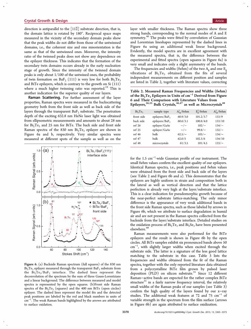
properties, Raman spectra were measured in the backscatteringgeometry both from the front side as well as back side of thelayers through the transparent BaF2 substrate. The penetrationdepth of the exciting 632.8 nm HeNe laser light was obtainedfrom ellipsometric measurements and amounts to about 28 nmfor Bi2Te3 and 25 nm for BiTe. The back side and front sideRaman spectra of the 830 nm Bi2Te3 epilayer are shown inFigure 6a and b, respectively. Very similar spectra weremeasured at different spots of the sample as well as on the
layer with smaller thickness. The Raman spectra show threestrong bands, corresponding to the normal modes of A and Esymmetry.46 The peaks were fitted by convolution of Gaussianand Lorentzian lineshapes represented by the dashed lines inFigure 6a using an additional weak linear background.Evidently, the model spectra are in excellent agreement withthe measured spectra, that is, the difference between theexperimental and fitted spectra (open squares in Figure 6a) isvery small and indicates only a slight asymmetry of the bands.The frequencies and widths (fwhm) of the two Ag and one Eg
vibrations of Bi2Te3 obtained from the fits of severalindependent measurements on different position and samplesare listed in Table 2, together with literature values, correcting
for the 1.5 cm−1-wide Gaussian profile of our instrument. Thesmall fwhm values confirm the excellent quality of our epilayers.Identical Raman spectra, i.e., peak positions and fwhm valueswere obtained from the front side and back side of the layers(see Table 2 and Figure 6b and a). This demonstrates that theepilayers are highly uniform in strain and composition both inthe lateral as well as vertical direction and that the latticeperfection is already very high at the layer/substrate interface.This is a clear indication for pseudomorphic growth because ofthe near-perfect substrate lattice-matching. The only minordifference is the appearance of very weak additional bands inthe front side Raman spectra, such as those labeled by arrows inFigure 6b, which we attribute to surface degradation in humidair and are not present in the Raman spectra collected from thebackside from the layer/substrate interface. Detailed studies onthe oxidation process of Bi2Te3 and Bi2Se3 have been presentedelsewhere.49
Raman measurements were also performed for the BiTeepilayers and the result is shown in Figure 6b by the opencircles. All BiTe samples exhibit six pronounced bands above 50cm−1, with slightly larger widths when excited through thesubstrate side. The latter is a signature of the less good latticematching to the substrate in this case. Table 3 lists thefrequencies and widths obtained from the fit of the Ramanspectra, together with the only reported literature data obtainedfrom a polycrystalline BiTe film grown by pulsed laserdeposition (PLD) on silicon substrate.31 Since 12 differentRaman−active bands are expected for the rather complex BiTestructure31 in a fairly narrow frequency interval, the relativelysmall widths of the Raman peaks of our samples (see Table 3)confirm the high quality of the layers found by our x−raystudies. The additional weak features at 72 and 75 cm−1 ofvariable strength in the spectrum from the film surface (arrowsin Figure 6b) are again attributed to surface oxidization.
Figure 6. (a) Backside Raman spectrum (full squares) of the 830 nmBi2Te3 epilayer measured through the transparent BaF2 substrate fromthe Bi2Te3/BaF2 interface. The dashed lines represent thedeconvolution of the spectrum by the sum of three Gauss-Lorentziansand a linear background. The difference between measured and modelspectra is represented by the open squares. (b)Front side Ramanspectra of the Bi2Te3 (squares) and the 400 nm BiTe (open circles)epilayer. The dashed lines represent the model fits and the detectedpeak positions are labeled by the red and black numbers in units ofcm−1. The weak Raman bands highlighted by the arrows are attributedto surface oxidation.
Table 2. Measured Raman Frequencies and Widths (fwhm)of the Bi2Te3 Epilayers in Units of cm−1 Derived from Figure6 and Their Comparison with Literature Values fromEpilayers,26,25 Bulk Crystals,46,47 as well as Microcrystals48
Bi2Te3 sample type A1g1 /fwhm Eg
2/fwhm A1g2 /fwhm
front side epilayers/BaF2 60.9/3.0 101.2/3.7 133/9back side epilayers/BaF2 60.6/3.1 100.8/4.0 133/10ref 26 epilayer/GaAs −/− 102/− 134/−ref 25 epilayer/GaAs −/− 99.8/− 132/−ref 46 bulk 62.5/− 103/− 134/−ref 47 bulk 62.0/5 102.3/6 134/10ref 48 microcrystals 61/3.5 101/4.5 133/−
Crystal Growth & Design Article
dx.doi.org/10.1021/cg400048g | Cryst. Growth Des. 2013, 13, 3365−33733370
Optical and Electronic Properties. The optical constantsof the Bi2Te3 and BiTe epilayers were determined over a widespectral range from the far-infrared to the ultraviolet (UV),combining spectroscopic ellipsometry and reflectivity measure-ments including synchrotron data acquired at NSLSBrookhaven. The near-normal incidence infrared reflectivitywas analyzed with the standard model of coherent interferenceswithin a layer on a substrate,50 assuming the dielectric functionof the layer in the Drude-Lorentz form as described in detail inthe Supporting Information.Figures 7a and b show the real part of the optical
conductivity σ1(ω) = −iωε0(ε(ω) − 1) derived for the BiTe
(black solid lines) and Bi2Te3 epilayers (blue dash-dottedlines), and Figure 7c and d the real part of the dielectricfunction ε1(ω). The dispersion of the optical constants wasobtained by the combination of reflectivity in the far-infrared,and ellipsometry at higher frequencies, using the variationaldielectric function approach.51 The Bi2Te3 sample is trans-parent in the energy range below about 0.2 eV and from theresulting interference fringes the layer thickness wasdetermined as 830 nm. The BiTe epilayer is only slightlytransparent below 0.2 eV because of much stronger free carrierabsorption. The corresponding thickness was obtained as (390± 5) nm close to the nominal value of 400 nm. The derivedpseudodielectric function of Bi2Te3 in the 0.6−6 eV range didnot exhibit any detectable angular dependence. Consequently,
it represents the in-plane response E ⊥ c. At these photonenergies the reported anisotropy of bulk Bi2Te3 is small.
52 Thecharacteristic energies of the spectral features seen in Figure 7bare in good agreement with those of bulk Bi2Te3 reported in ref52.For BiTe, the absorption above 0.3 eV is due to interband
transitions, dominated by the strong band at 1.35 eV, and sidebands at 0.42 and 2.7 eV as indicated by the arrows in Figure7b. This structure is similar to that of Bi2Te3, which isrepresented by the blue dash-dotted line for comparison. Theinterband transitions are likely related to the Bi−Te bilayer,which is the basic building block of both the Bi2Te3 and BiTestructure (see Figure 1). The weaker band at 0.18 eV in BiTe(see Figure 7a) is related to the 0.15 eV structure in Bi2Te3reported in ref 52. At lower energies, the increase of the realpart of conductivity and the decrease of the real part of thedielectric function with the decreasing photon frequency arisesfrom the strong contribution of conducting electrons. Theanalysis of the spectra using the Drude model yields ωpl = 1.58± 0.04 eV and γ = 0.09 ± 0.01 eV. Using
ωε
=*
nqmpl
22
0 (1)
where n is the carrier concentration and q and m* the chargeand effective mass, the free carrier concentration in BiTe isfound to be about 20 times larger than in Bi2Te3, assuming theeffective masses are roughly the same. Since our X-ray andRaman measurements have revealed a high crystallineperfection of the samples and no signatures of increasedbroadening is found in the optical spectra, this high carrierconcentration in BiTe is probably not caused by extrinsic effectslike vacancies but rather by a metal-like band structure,involving a band that crosses the Fermi level. This conclusion issupported by the analysis of the second BiTe sample thatyielded also a large value of the plasma frequency (1.45 eV). Toour knowledge, no calculations of the BiTe band structure havebeen available; however, calculations of the isostructural BiSecompound53 show several bands crossing the Fermi level in thedirection perpendicular to the c-axis, which supports ourconclusion.To confirm the large difference in the carrier concentration
of the BiTe and Bi2Te3 layers, we have measured the DCelectric and Hall conductivities by the Van der Pauw method.The DC conductivity of BiTe amounts to 3700 ± 200 ω−1
cm−1. The Hall effect measurement revealed n-type con-ductivity with a carrier concentration of 7 ± 1 × 1020 cm−3
using a Hall factor of unity. From this carrier concentration andthe measured plasma frequency, we derive the effective electronmass to be about 0.37 ± 0.05 me in BiTe. Since the Hall effectmeasurement on the Bi2Te3 samples were hampered by theEttingshausen effect, we have measured the thermoelectricSeebeck coefficient instead, giving S = 170 ± 20 mV K−1 at 300K, which yields a free electron concentration of 1.3 ± 0.3 ×1019 cm−3 (see ref 54), which is more than 1 order ofmagnitude lower than for the BiTe epilayer, in agreement with
Table 3. Measured Raman Frequencies and Widths (fwhm) of the Bi1Te1 Epilayers in Units of cm−1 Derived from Figure 6bCompared to Literature Values Obtained for Polycrystalline Pulsed Laser Deposited (PLD) Films31
BiTe sample type ν/fwhm ν/fwhm ν/fwhm ν/fwhm ν/fwhm ν/fwhm
front side epilayers/BaF2 60.0/3.3 83/2.8 92.3/4.7 101.6/9 122/6 128/7back side epilayers/BaF2 59.0/4.5 83/10 90.8/6 101.9/11 120/7 126/17ref 31 PLD films 88/− 117/−
Figure 7. Real part of conductivity (top) and real part of the dielectricfunction (bottom) of BiTe (black solid lines) and of Bi2Te3 (bluedash-dotted lines) added for comparison. For clarity the spectra for thefar-infrared (left) and near-infrared−ultraviolet ranges (right) aredisplayed on different scales. The dots in panel a correspond to themeasured dc conductivity measured in van der Pauw geometry.
Crystal Growth & Design Article
dx.doi.org/10.1021/cg400048g | Cryst. Growth Des. 2013, 13, 3365−33733371

the optical data. The DC conductivity of Bi2Te3 amounts to160 ± 30 ω−1 cm−1. The DC conductivities derived from theelectrical measurements are indicated in Figure 7a by the black,respectively, and blue dot on the ordinate axis. Clearly, thevalues agree well with the low-energy extrapolation of theinfrared conductivity measurements, demonstrating a goodconsistency of our data.To further assess the quality of the epilayers, we have
performed angle resolved photoemission (ARPES) measure-ment of the electronic dispersion at the UE112-PGM2abeamline of BESSY II in Berlin under ultrahigh vacuumconditions at room temperature. For protection of the samples,the surface was capped in situ after by a 100 nm Te cappinglayer, which was desorbed in the photoemission chamber atBESSY just before the ARPES experiments. The resultingthree-dimensional band dispersion is presented in Figure 8 for
Bi2Te3 grown under the same conditions as described above.Identical ARPES spectra were obtained from different places ofthe sample, indicating a high uniformity of the samples in thelateral direction. The topologically protected surface state(TSS) indicated by the dashed line in Figure 8b shows theexpected linear dispersion with the Dirac point overlappingwith the bulk valence band (BVB). The dispersion of thesurface state deviates from the simple isotropic Dirac cone ofBi2Se3,
6 showing a significant hexagonal warping of the banddispersion at the Fermi level, as can be seen at the top of theARPES map displayed in Figure 8a. According to the ARPESmeasurements, the bottom of the bulk conduction band (BCB)lies about ∼130 meV below the Fermi level (see Figure 8b),which compares very well to the value of 120 meV calculatedfrom the bulk electron concentration 1.3 × 1019 cm−3. Thisindicates that the free electron concentration at the surfaceassessed by ARPES does not differ significantly from the bulkconcentration. Therefore, the Se capping and subsequentpreparation of the clean surface for ARPES measurement by
annealing does not produce a charge density on the surface.The ARPES results are in nice agreement with previoustheoretical and experiments on the electronic band structure ofBi2Te3.
7 This demonstrates that the structural quality of theepitaxial bismuth telluride layers is very well suited for studiesof the band structure of both bulk and topological surfacestates. Preliminary ARPES measurements on BiTe epilayers donot show a 2D surface state, which is an indication that BiTe isnot a topological insulator.
■ CONCLUSIONIn summary, we have demonstrated heteroepitaxial growth ofdifferent bismuth telluride phases onto BaF2 (111) substratesusing molecular beam epitaxy. The stoichiometric compositionof the layers was adjusted by control of the Te flux providedduring growth and single phase hexagonal BiTe and Bi2Te3epilayers were obtained at low and high excess Te flux,respectively. The layers grow with their c-axis perpendicular tothe surface and due to the good lattice matching to the BaF2substrate, a high structural perfection was obtained. The strain,size and tilts of the coherently scattering domains weredetermined by high resolution X-ray reciprocal space mapping,revealing a better structural perfection of Bi2Te3 compared toBiTe due to the almost perfect substrate lattice matching. Thisis supported by Raman measurements that show a low defectconcentration and high crystalline quality present at theBi2Te3/BaF2 interface. This suggests that the layer/substratelattice-mismatch is an important parameter for heteroepitaxialgrowth of bismuth telluride epilayers, in spite of the van derWaals bonding present in the crystal structure.For both bismuth telluride phases, the Raman modes,
electronic structure, and optical properties were derived fromspectroscopic measurements and the plasma frequency of freeelectrons as well as the interband transitions were deduced. Byangular resolved photoemission spectroscopy, the three-dimen-sional dispersion of the topologically protected surface statewas measured for Bi2Te3 epilayers, revealing the Dirac point atthe top of the bulk valence band and a strong hexagonalwarping of the surface state at higher energies. The position ofthe Fermi level probed by photoelectron spectroscopy wasfound to be in good agreement with the carrier concentrationin the bulk derived from transport measurements. Thus, theemployed sample preparation produces very clean surfaces forphotoemission studies. Infrared and transport measurementsindicate a bulk metallic character of the BiTe material with amore than one order of magnitude higher carrier concentrationas compared to Bi2Te3. To the best of our knowledge, thegrowth of epitaxial layers and infrared optical measurements ofthe BiTe phase was demonstrated for the first time. The smalllattice mismatch between BiTe and Bi2Te3 provides goodconditions for fabrication of heterostructures and superlatticesof the two phases. This may open a new pathway for realizationof topological insulator structures.
■ ASSOCIATED CONTENT*S Supporting InformationAdditional information and figures showing optical properties,This material is available free of charge via the Internet athttp://pubs.acs.org.
■ AUTHOR INFORMATIONCorresponding Author*E-mail: [email protected].
Figure 8. Band dispersion of the Bi2Te3 epilayers measured by angularresolved photoemission (ARPES). Panel (a) on the left shows thethree-dimensional map of the photoemission intensity in the vicinity ofthe Γ point. The Fermi level is at 0 eV, and the kx axis corresponds tothe Γ−K direction in the hexagonal two-dimensional surface Brillouinzone and the ky axis to Γ−M direction. Panel b shows the 2Ddispersion (first derivative of the photoemission intensity with respectto energy) in the kx direction. The dashed line indicates thetopologically protected surface state (TSS). BCB denotes the bulkconduction band and BVB the bulk valence band. The measurementswere performed using ℏν = 21 eV photons for excitation.
Crystal Growth & Design Article
dx.doi.org/10.1021/cg400048g | Cryst. Growth Des. 2013, 13, 3365−33733372

FundingThe work was supported by the CSF grant P204/12/0595. Useof the National Synchrotron Light Source, BrookhavenNational Laboratory, was supported by the U.S. Departmentof Energy, Office of Science, Office of Basic Energy Sciences,under Contract No. DE-AC02-98CH10886. Near-IR-VISellipsometry measurements at the Center for FunctionalNanomaterials, Brookhaven National Laboratory, have beensupported by DOE DE-AC02-98CH10886.
NotesThe authors declare no competing financial interest.
■ REFERENCES(1) Hasan, M. Z.; Kane, C. L. Rev. Mod. Phys. 2010, 82, 3045.(2) Zhang, H.; Liu, C.; Qi, X.; Dai, X.; Fang, Z.; Zhang, S. Nat. Phys.2009, 5, 438.(3) Hsieh, D.; Xia, Y.; Qian, D.; Wray, L.; Meier, F.; Dil, J.;Osterwalder, J.; Patthey, L.; Fedorov, A.; Lin, H.; et al. Phys. Rev. Lett.2009, 103, 146401.(4) Qu, D.; Hor, Y.; Xiong, J.; Cava, R.; Ong, N. Science 2010, 329,821.(5) Qi, X.-L.; Zhang, S.-C. Rev. Mod. Phys. 2011, 83, 1057.(6) Xia, Y.; Wray, L.; Qian, D.; Hsieh, D.; Pal, A.; Lin, H.; Bansil, A.;Grauer, D.; Hor, Y.; Cava, R.; et al. Nat. Phys. 2009, 5, 398.(7) Chen, Y. L.; Analytis, J. G.; Chu, J.-H.; Liu, Z. K.; Mo, S.-K.; Qi,X. L.; Zhang, H. J.; Lu, D. H.; Dai, X.; Fang, Z.; et al. Science 2009,325, 178.(8) Roushanm, P.; Seo, J.; Parker, C. V.; Hor, Y. S.; Hsieh, D.; Qian,D.; Richardella, A.; Hasan, M. Z.; Cava, R. J.; Yazdani, A. Nature 2009,460, 1106.(9) Moore, J. E. Nature 2010, 464, 194.(10) Alpichshev, Z.; Analytis, J. G.; Chu, J. H.; Fisher, I. R.; Chen, Y.L.; Shen, Z. X.; Fang, A.; Kapitulnik, A. Phys. Rev. Lett. 2010, 104,016401.(11) Zhang, T.; Cheng, P.; Chen, X.; Jia, J.-F.; Ma, X.; He, K.; Wang,L.; Zhang, H.; Dai, X.; Xie, Z. F. X.; et al. Phys. Rev. Lett. 2009, 103,266803.(12) Tritt, T. Science 1999, 283, 804.(13) Snyder, G. J.; Toberer, E. S. Nat. Mater. 2008, 7, 195.(14) Hsieh, D.; Xia, Y.; Qian, D.; Wray, L.; Dil, J. H.; Meier, F.;Osterwalder, J.; Patthey, L.; Checkelsky, J. G.; Ong, N. P.; et al. Nature2009, 460, 1101.(15) He, L.; Kou, X.; Wang, K. L. Phys. Status Solidi RRL 2013, 7, 50.(16) He, X.; Guan, T.; Wang, X.; Feng, B.; Cheng, P.; Chen, L.; Li,Y.; Wu, K. Appl. Phys. Lett. 2012, 101, 123111.(17) Liu, H. W.; Yuan, H. T.; Fukui, N.; Zhang, L.; Jia, J. F.; Iwasa, Y.;Chen, M. W.; Hashizume, T.; Sakurai, T.; Xue, Q. K. Cryst. GrowthDesign 2010, 10, 4491.(18) Chen, X.; Ma, X.-C.; Jia, J.-F.; Xue, Q.-K. Adv. Mater. 2011, 23,1162.(19) Krumrain, J.; Mussler, G.; Borisova, S.; Stoica, T.; Plucinski, L. J.Cryst. Growth 2011, 324, 115.(20) Borisova, S.; Krumrain, J.; Luysberg, M.; Mussler, G.;Grutzmacher, D. Cryst. Growth Design 2012, 12, 6098.(21) Fukui, N.; Hirahara, T.; Shirasawa, T.; Takahasi, T.; Kobayashi,K.; Hasegawa, S. Phys. Rev. B 2012, 85, 115426.(22) Li, Y.-Y.; Wang, G.; Zhu, X.-G.; Liu, M.-H.; Ye, C.; Chen, X.;Wang, Y.-Y.; He, K.; Wang, L.-L.; Ma, X.-C.; et al. Adv. Mater. 2010,22, 4002.(23) Plucinski, L.; Mussler, G.; Krumrain, J.; Herdt, A.; Suga, S.;Grutzmacher, D.; Schneider, C. M. Appl. Phys. Lett. 2011, 98, 222503.(24) Zhang, S. X.; Yan, L.; Qi, J.; Zhuo, M.; Wang, Y.-Q.;Prasankumar, R.; Jia, Q.; Picraux, S. Thin Solid Films 2012, 21, 6459.(25) Cao, H.; Venkatasubramanian, R.; Liu, C.; Pierce, J.; Yang, H.;Hasan, M. Z.; Wu, Y.; Chen, Y. P. Appl. Phys. Lett. 2012, 101, 132104.
(26) Liu, X.; Smith, D. J.; Fan, J.; Zhang, Y.-H.; Cao, H.; Chen, Y. P.;Leiner, J.; Kirby, B. J.; Dobrowolska, M.; Furdyna, J. K. Appl. Phys. Lett.2011, 99, 171903.(27) Massalski, T. B.; Okamoto, H. Binary Alloy Phase Diagrams;ASM International: Materials Park, OH, 1996.(28) Kim, Y.; Cho, S.; DiVenere, A.; Wong, G. K. L.; Ketterson, J. B.Phys. Rev. B 2001, 63, 155306.(29) Bos, J. W. G.; Zandbergen, H. W.; Lee, M.-H.; Ong, N. P.; Cava,R. J. Phys. Rev. B 2007, 75, 195203.(30) Yamana, K.; Kihara, K.; Matsumoto, T. Acta Crystallogr. B 1979,35, 147.(31) Russo, V.; Bailini, A.; Zamboni, M.; Passoni, M.; Conti, C.;Casari, C. S.; Bassi, A. L.; Bottani, C. E. J. Raman Spectrosc. 2008, 39,205.(32) Peranio, N.; Eibl, O.; Nurnus, J. J. Appl. Phys. 2006, 100,114306.(33) Madelung, O. Semiconductors: Data Handbook; Springer-Verlag:Berlin, 2004.(34) Wyckoff, R. W. G. Crystal Structures, Vol. 2; Wiley, New York,1964.(35) Nakajima, S. J. Phys. Chem. Sol. 1963, 24, 479.(36) Natl. Bur. Stand. (U.S.) Monogr. 1964, 253, 16.(37) Shimazakí, H.; Ozawa, T. Am. Mineral. 1978, 63, 1162.(38) Stasova, M. M.; Strukt., Zh. Khim 1967, 8, 655.(39) Hayes, W. Crystals with Fluoride Structure; Clarendon: Oxford,U.K., 1974.(40) Teweldebrhan, D.; Goyal, V.; Balandin, A. A. Nano Lett. 2010,10, 1209.(41) Pietsch, U.; Holy, V.; Baumbach, T. High-Resolution X-RayScattering From Thin Films to Lateral Nanostructures; Springer-Verlag:Berlin, 2004.(42) Holy, V.; Kubena, J.; Abramof, E.; Lischka, K.; Pesek, A.;Koppensteiner, E. J. Appl. Phys. 1993, 74, 1736.(43) Tarakina, N. V.; Schreyeck, S.; Borzenko, T.; Schumacher, C.;Karczewski, G.; Brunner, K.; Gould, C.; Buhmann, H.; Molenkamp, L.W. Cryst. Res. Design 2012, 12, 1913.(44) Schreyeck, S.; Tarakina, N. V.; Karczewski, G.; Schumacher, C.;Borzenko, T.; Brune, C.; Buhmann, H.; Gould, C.; Brunner, K.;Molenkamp, L. W. Appl. Phys. Lett. 2013, 102, 041914.(45) Jenkins, J. O.; Rayne, J. A.; Ure, J. R. W. Phys. Rev. B 1972, 3,3171.(46) Richter, W.; Kohler, H.; Becker, C. Phys. Status Solidi B 1977,84, 619.(47) Kullmann, W.; Geurts, J.; Richter, W.; Lehner, N.; Rauh, H.;Steigenberger, U.; Eichhorn, G.; Geick, R. Phys. Status Solidi B 1984,125, 131.(48) Atuchin, V.; Gavrilova, T.; Kokh, K.; Kuratieva, N.; Pervukhina,N.; Surovtsev, N. Solid State Commun. 2012, 152, 1119.(49) Yashina, L. V.; Sanchez-Barriga, J.; Scholz, M. R.; Volykhov, A.A.; Sirotina, A. P.; Neudachina, V. S.; Tamm, M. E.; Varykhalov, A.;Marchenko, D.; Springholz, G.; Bauer, G.; Knop-Gericke, A.; Rader, O.ACS Nano 2013, 7, 5181.(50) Azzam, R. M. A.; Bashara, N. M. Ellipsometry and PolarizedLight; Elsevier Science Publisher: Amsterdam, 1987.(51) Kuzmenko, A. B. Rev. Sci. Instrum. 2005, 76, 083108.(52) Greenaway, D. L.; Harbeke, G. J. Phys. Chem. Solids 1965, 26,1585.(53) Gaudin, E.; Jobic, S.; Evain, M.; Brec, R.; Rouxel, J. Mater. Res.Bull. 1995, 30, 549.(54) Mishra, S. K.; Satpathy, S.; Jepsen, O. J. Phys.: Condens. Matter1997, 9, 461.
Crystal Growth & Design Article
dx.doi.org/10.1021/cg400048g | Cryst. Growth Des. 2013, 13, 3365−33733373


![Structure and functional properties of epitaxial PbZrxTi O3 films...epitaxial films[11][12]. Once the high quality epitaxial PZT films are made these can be used to better understand](https://img.dokumen.tips/doc/110x75/60df425bb5812e17d635303f/structure-and-functional-properties-of-epitaxial-pbzrxti-o3-films-epitaxial.jpg)


