Embed Size (px)
Citation preview

Graphic LCD Display 240*128
Model No: LCD240128A
LEDSEE electronics Website: www.ledsee.com
Email: [email protected]
April 8, 2007 Version 1.0

LEDSEE electronics
Website: www.ledsee.com Email: [email protected]
CONTENTS
1. FEATURES- - - - - - - - - - - - - - - - - - - - - - - - - - - - - - - - - - - - - - - - - - - - - - - - 1
2. BLOCK DIAGRAM &APPLICATION CIRCUIT - - - - - - - - - - - - - - - - - - - - - - - 1
3. OUTLINE DIMENSIONS- - - - - - - - - - - - - - - - - - - - - - - - - - - - - - - - - - - - - - 3
4. ABSOLUTE MAXIMUM RATING - - - - - - - - - - - - - - - - - - - - - - - - - - - - - - - - 4
5. ELECTRICAL CHARACTERISTICS - - - - - - - - - - - - - - - - - - - - - - - - - - - - - - 4
6. OPTICAL CHARACTERISTICS- - - - - - - - - - - - - - - - - - - - - - - - - - - - - - - - - - 5
7. TIMING CHARACTERISTICS - - - - - - - - - - - - - - - - - - - - - - - - - - - - - - - - - - 6
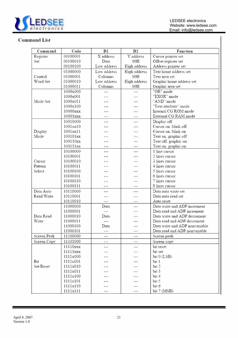
8. DISPLAY CONTROL INSTRUCTION- - - - - - - - - - - - - - - - - - - - - - - - 8
9. INTERFACE PIN CONNECTIONS- - - - - - - - - - - - - - - - - - - - - - - - - - - 23
10. RELIABILITY- - - - - - - - - - - - - - - - - - - - - - - - - - - - - - - - - - - - - - - - - - - - 25
11. QUALITY GUARANTEE- - - - - - - - - - - - - - - - - - - - - - - - - - - - - - - - - - - 26
12. INSPECTION CRITERIA- - - - - - - - - - - - - - - - - - - - - - - - - - - - - - - - - - - 27
13. PRECAUTIONS FOR USING LCD MODULES- - - - - - - - - - - - - - - - - 30
14. USING LCD MODULES- - - - - - - - - - - - - - - - - - - - - - - - - - - - - - - - - - - - 31
April 8, 2007 Version 1.0

LEDSEE electronics Website: www.ledsee.com Email: [email protected]
April 8, 2007 Version 1.0
1
1. FEATURES: ITEM STANDARD VALUE UNIT
Display Type 240 *128 dots - LCD Type ■STN, BLUE, Transflective, Negative, Extend TEMP - □STN, GREY, Transflective, Position, Extend TEMP □STN, YELLOW-GREEN, Transflective, Position, Extend
TEMP
□FSTN, Position, Extend TEMP LCD Duty 1/128 - LCD Bias 1/12 - Viewing Direction 6:00 - Backlight Type ■LED(White) - □LED(Yellow-Green) Interface 6800 Series or 8080 series - Driver IC ■ T6963 - □ T6A39,T6A40 (No controller) Module Dimension 144.0(W) X 104.0 (H) X12.0 (MAX)(T) mm Effective Display Area 107.95 (W) X57.55 (H) mm Dot Size 0.40 (W) X 0.40 (H) mm Dot Pitch 0.45 W) X 0.45 (H) mm
2. BLOCK DIAGRAM & APPLICATION CIRCUIT:

LEDSEE electronics Website: www.ledsee.com Email: [email protected]
April 8, 2007 Version 1.0
2
Bulit-in T6963 Application
T6A39/T6A40 (No controller) Application

LEDSEE electronics Website: www.ledsee.com Email: [email protected]
April 8, 2007 Version 1.0
3
3. OUTLINE DIMENSIONS

LEDSEE electronics Website: www.ledsee.com Email: [email protected]
April 8, 2007 Version 1.0
4
4. ABSOLUTE MAXIMUM RATING
STANDARD VALUE ITEM SYMBOL CONDITION MIN TYP MAX
UNIT
POWER SUPPLY FOR LOGIC VDD Ta=25℃ -0.3 - 7.0 V INPUT VOLTAGE VIN Ta=25℃ -0.3 - VDD+0.3 V Module OPERATION TEMPERATURE TOPR --- -20 - +70 ℃
Module STORAGE TEMPERATURE TSTG --- -30 - +80 ℃
Storage Humidity HD Ta < 40 °C - 90 %RH
5. ELECTRICAL CHARACTERISTICS
ITEM SYMBOL CONDITION MIN TYP MAX UNIT Supply Voltage (logic) VDD-VSS - 4.5 5 5.5 V
Supply Voltage (LCD) VDD-V0 Ta= +25℃ Blue
Ta= +25℃ Y-G - -18.5 -18.5 - V
V-IH “H” level VDD-2.2 - VDD V Input signal voltage
V-IL “L” level 0 - 0.8 V V-OH “H” level VDD-0.3 - VDD V
Output signal voltage VOL “H” level 0 - 0.3 V
Supply Current (logic) IDD VDD=5.0V - - - mA
Backlight Voltage V-BL LED(Yellow-Green) LED(White) -
4.2V 3.1 - V
Backlight Current I-BL LED(Yellow-Green) LED(White) -70
200 130 -150 mA
Backlight Driver Wave - - - kHz Backlight Brightness Backlight Life Time
LEDSEE electronics Website: www.ledsee.com Email: [email protected]
April 8, 2007 Version 1.0
5
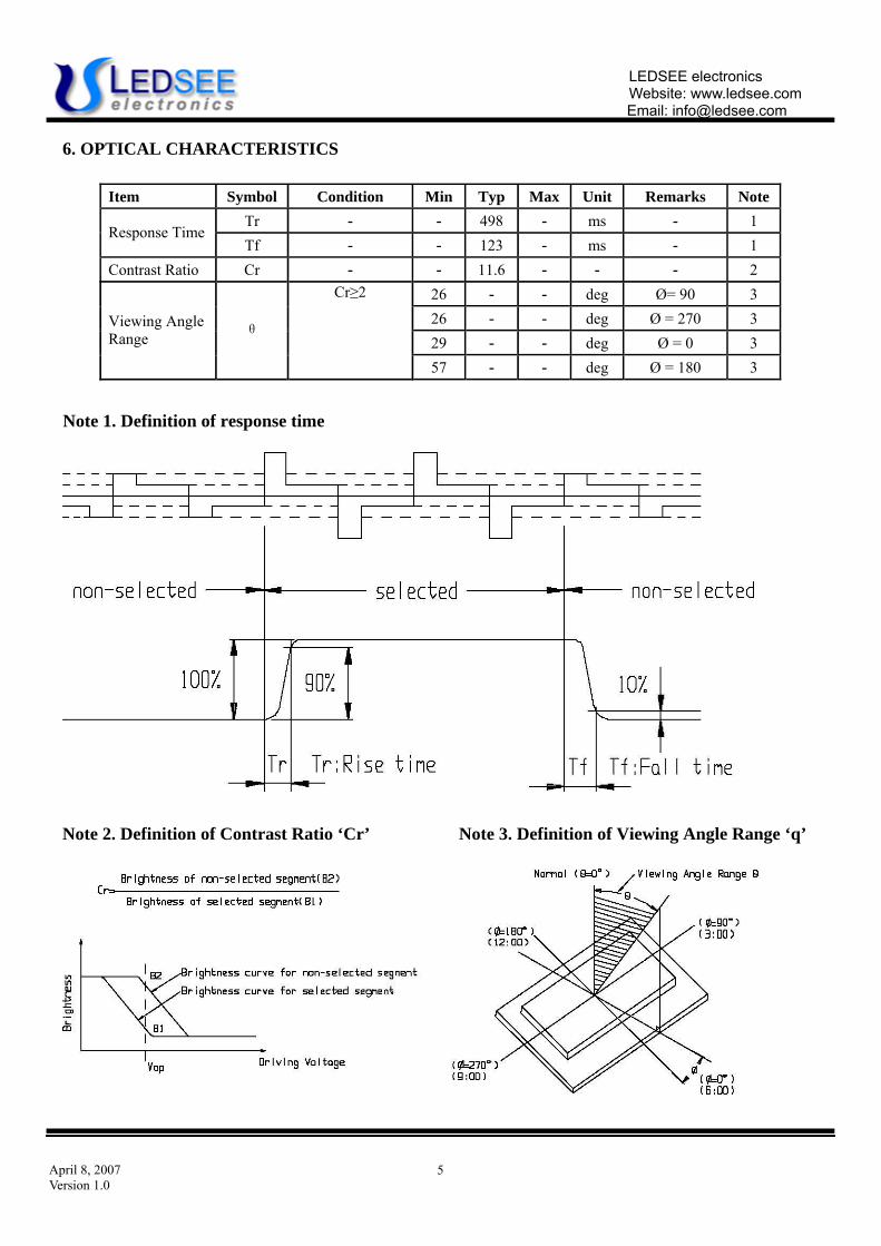
6. OPTICAL CHARACTERISTICS
Item Symbol Condition Min Typ Max Unit Remarks Note Tr - - 498 - ms - 1
Response Time Tf - - 123 - ms - 1
Contrast Ratio Cr - - 11.6 - - - 2 26 - - deg Ø= 90 3 26 - - deg Ø = 270 3 29 - - deg Ø = 0 3
Viewing Angle Range θ
Cr≥2
57 - - deg Ø = 180 3
Note 1. Definition of response time
Note 2. Definition of Contrast Ratio ‘Cr’ Note 3. Definition of Viewing Angle Range ‘q’

LEDSEE electronics Website: www.ledsee.com Email: [email protected]
April 8, 2007 Version 1.0
6
7. TIMING CHARACTERISTICS
7.1 T6963 Timing
LEDSEE electronics Website: www.ledsee.com Email: [email protected]
April 8, 2007 Version 1.0
7
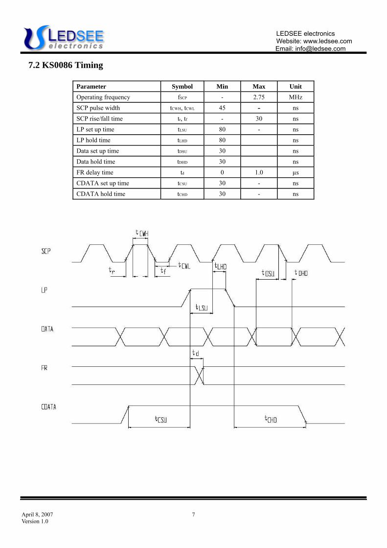
7.2 KS0086 Timing
Parameter Symbol Min Max Unit Operating frequency fSCP - 2.75 MHz
SCP pulse width tCWH, tCWL 45 - ns
SCP rise/fall time tr, tf - 30 ns
LP set up time tLSU 80 - ns
LP hold time tLHD 80 ns
Data set up time tDSU 30 ns
Data hold time tDHD 30 ns
FR delay time td 0 1.0 µs
CDATA set up time tCSU 30 - ns
CDATA hold time tCHD 30 - ns
LEDSEE electronics Website: www.ledsee.com Email: [email protected]
April 8, 2007 Version 1.0
8
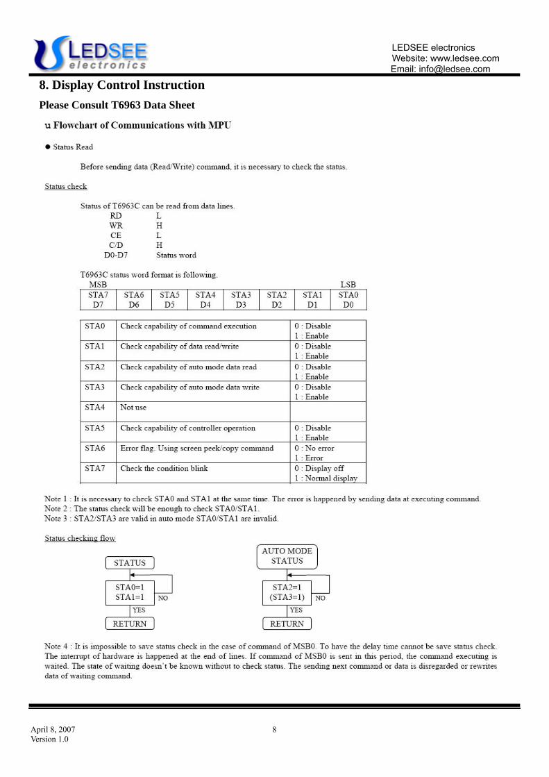
8. Display Control Instruction Please Consult T6963 Data Sheet

LEDSEE electronics Website: www.ledsee.com Email: [email protected]
April 8, 2007 Version 1.0
23
9. INTERFACE PIN CONNECTIONS
PIN SYMBOL I/O FUNCTION 1 FG Frame Ground 2 VSS I Ground pin, connected to 0V 3 VDD I Power supply pin for logic .(+5V) 4 V0 I Contrast control (VDD~VOUT) 5 /WR I Data write:
Write data into T6963 when /WR is L. 6 /RD I Data Read:
Read data from T6963 when /RD is L. 7 /CE I Chip enable for T6963:
/CE must be L when CPU communicates with T6963 C/D /WR=L /RD =L L Data Write Data Read
8 C/D I
H Command Write Status Read 9 RESET I Reset signal:
H: Normal (T6963 has internal pull-up resistor)
L: Initialize T6963. Text and graphic have address and text and graphic area setting are retained.
10 DB0 I/O Data I/O pins for display memory. 11 DB1 I/O Data I/O pins for display memory. 12 DB2 I/O Data I/O pins for display memory. 13 DB3 I/O Data I/O pins for display memory. 14 DB4 I/O Data I/O pins for display memory. 15 DB5 I/O Data I/O pins for display memory. 16 DB6 I/O Data I/O pins for display memory. 17 DB7 I/O Data I/O pins for display memory. 18 FS I- Pin for selection of font: FS=H: 7×8 dots FS=L: 8×8 dots 19 VOUT O Power output , LCD power supply 20 LEDA I LED anode (+5V) 21 LEDK I LED cathode (0V) 22 NC No connect 23 ED Display data input 24 CDATA Frame signal 25 FR AC signal for LCD driver output
Alternate signal input pin for LCD driving. Normal frame inversion signal is input in to this pin.
26 LP Data latch clock
LEDSEE electronics Website: www.ledsee.com Email: [email protected]
April 8, 2007 Version 1.0
24
this signal is used for latching the shift register contents at the falling edge of this
clock pulse. CL1 pulse "High" level initializes power-down function block.
27 HSCP Clock pulse input for the bi-directional shift register. the data is shifted to 20 x 4-bit segment data shift The clock pulse, which was input when the enable bit (ELB/ERB) is in not active condition, is invalid.
28 NC No connect 29 VDD Power supply pin for logic .(+5V) 30 VSS Ground pin, connected to 0V 31 V0 Contrast control (VDD~VOUT) 32 VOUT Power output , LCD power supply 33 LEDA LED anode (+5V) 34 LEDK LED cathode (0V)

LEDSEE electronics Website: www.ledsee.com Email: [email protected]
April 8, 2007 Version 1.0
25
10. RELIABILITY
Content of Reliability Test Environmental Test
No. Test Item Content of Test Test Condition Applicable
Standard 1 High temperature
storage Endurance test applying the high storage temperature for a long time. 80℃ 200 hrs
2 Low temperature storage
Endurance test applying the low storage temperature for a long time. -30℃ 200 hrs
3 High temperature operation
Endurance test applying the electric stress (Voltage & Current) and the thermal stress to the element for a long time.
70℃ 200 hrs
4 Low temperature operation
Endurance test applying the electric stress under low temperature for a long time. -20℃ 200 hrs
5 High temperature Humidity storage
Endurance test applying the high temperature and high humidity storage for a long time.
50 ℃ , 90 96 hrs
RH MIL-202E-103B JIS-C5023
6 High temperature Humidity operation
Endurance test applying the electric stress (Voltage & Current) and temperature humidity stress to the element for a long time.
50 ℃ , 90 96 hrs
RH MIL-202E-103B JIS-C5023
7 Temperature cycle Endurance test applying the low and high temperature cycle.
-20℃ -70℃10 cycles
Mechanical Test
8 Vibration test Endurance test applying the vibration during transportation and using. 10-22Hz→1.5mmp-p
MIL-202E-201A JIS-C5025
22-500Hz →1.5G
JIS-C7022-A-10
Total 0.5hrs
9 Shock test Constructional and mechanical endurance test 50G half sign wave 1l MIL-202E-213B
applying the shock during transportation. msedc 3 times of each direction 10 Atmospheric
pressure test Endurance test applying the atmospheric pressure during transportation by air.
115 mbar 40 hrs MIL-202E-105C
Others
11 Static electricity test
Endurance test applying the electric stress to the terminal.
VS=800V, RS=1.5 k CS=100 pF
MIL-883B-3015.1
1 time
∗∗∗ Supply voltage for logic system = 3V. Supply voltage for LCD system = Operating voltage at 25℃.

LEDSEE electronics Website: www.ledsee.com Email: [email protected]
April 8, 2007 Version 1.0
26
Failure Judgement Criterion
Test Item No. Failure Judgment Criterion Criterion Item
1 2 3 4 5 6 7 8 9 10 11 Basic specification Out of the Basic Specification
Electrical characteristic Out of the DC and AC Characteristic
Mechanical characteristic
Out of the Mechanical Specification Color change: Out of Limit Appearance Specification
Optical characteristic Out of the Appearance Standard
11. QUALITY GUARANTEE Acceptable Quality Level
Each lot should satisfy the quality level defined as follows. - Inspection method: MIL-STD-105E LEVEL II Normal one time sampling - AQL
Partition AQL Definition A: Major 0.4% Functional defective as product B: Minor 1.5% Satisfy all functions as product but not satisfy cosmetic standard
Definition of ‘LOT’
One lot means the delivery quantity to customer at one time.
Conditions of Cosmetic Inspection Environmental condition
The inspection should be performed at the 1cm of height from the LCD module under 2 pieces of
40W white fluorescent lamps (Normal temperature 20∼25℃and normal humidity 60±15%RH).
Inspection method The visual check should be performed vertically at more than 30cm distance from the LCD panel.
Driving voltage The VO value which the most optimal contrast can be obtained near the specified VO in the
specification. (Within ±0.5V of typical value at 25℃.).
LEDSEE electronics Website: www.ledsee.com Email: [email protected]
April 8, 2007 Version 1.0
27
12. INSPECTION CRITERIA
12.1 Module Cosmetic Criteria
No. Item Judgement Criterion Partition 1 Difference in Spec. None allowed Major 2 Pattern peeling No substrate pattern peeling and floating Major 3 Soldering defects No soldering missing Major
No soldering bridge Major No cold soldering Major
4 Resist flaw on substrate
Invisible copper foil (′0.5mm or more) on substrate pattern Minor
5 Accretion of metallic No soldering dust No accretion of metallic foreign matters Minor Foreign matter (Not exceed ′0.2mm) Minor
6 Stain No stain to spoil cosmetic badly Minor 7 Plate discoloring No plate fading, rusting and discoloring Minor 8 Solder amount a. Soldering side of PCB Minor
Solder to form a ‘Filet’ all around the lead. Solder should not hide the 1. Lead parts lead form perfectly. (too much) b. Components side ( In case of ‘Through Hole PCB’ )
Solder to reach the Components side of PCB.
2. Flat packages Either ‘Toe’ (A) or ‘Seal’ (B) of the lead to be covered by ‘Filet’.
Minor
Lead form to be assume over solder. A B
3. Chips (3/2) H≥h ≥(1/2) H Minor

LEDSEE electronics Website: www.ledsee.com Email: [email protected]
April 8, 2007 Version 1.0
28
12.2 Screen Cosmetic Criteria (Non-Operating)
No. Defect Judgement Criterion Partition 1 Spots In accordance with Screen Cosmetic Criteria (Operating) No.1. Minor 2 Lines In accordance with Screen Cosmetic Criteria (Operating) No.2. Minor 3 Bubbles in Minor
polarizer
4 Scratch In accordance with spots and lines operating cosmetic criteria. Minor When the light reflects on the panel surface, the scratches are not to be remarkable.
5 Allowable density Above defects should be separated more than 30mm each other. Minor
6 Coloration Not to be noticeable coloration in the viewing area of the LCD Minor panels. Back-lit type should be judged with back-lit on state only. 7 Contamination Not to be noticeable. Minor
12.3. Screen Cosmetic Criteria (Operating)
No. Defect Judgement Criterion Partition 1 Spots A) Clear Note: Minor
Including pin holes and defective dots which must be within one pixel size. B) Unclear Size:

LEDSEE electronics Website: www.ledsee.com Email: [email protected]
April 8, 2007 Version 1.0
29
2 Lines A) Clear Minor
Note: ( ) - Acceptable Qty in active area L
-Length (mm) W - Width (mm) ∞ - Disregard
B) Unclear
‘Clear’ = The shade and size are not changed by VO. ‘Unclear’ = The shade and size are changed by VO.
12.4. Screen Cosmetic Criteria (Operating) (Continued) No. Defect Judgement Criterion Partition 3 Rubbing line Not to be noticeable. 4 Allowable density Above defects should be separated more than 10mm each other. Minor 5 Rainbow Not to be noticeable. Minor 6 Dot size To be 95% ∼105%of the dot size (Typ.) in drawing. Partial
defects of each dot (ex. pin-hole) should be treated as ‘Spot’. (see Screen Cosmetic Criteria (Operating) No.1)
Minor
7 Uneven brightness (only back-lit type module)
Uneven brightness must be BMAX / BMIN ≤ 2 - BMAX: Max. value by measure in 5 points - BMIN: Min. value by measure in 5 points
Divide active area into 4 vertically and horizontally. Measure 5 points shown in the following figure.
Minor

LEDSEE electronics Website: www.ledsee.com Email: [email protected]
April 8, 2007 Version 1.0
30
Note: (1) Size: d = (long length + short length) / 2 (2) The limit samples for each item have priority. (3) Complexed defects are defined item by item, but if the number of defects are defined in above
table, the total number should not exceed 10. (4) In case of ‘concentration’, even the spots or the lines of ‘disregarded’ size should not allowed.
Following three situations should be treated as ‘concentration’. - 7 or over defects in circle of ′5mm. - 10 or over defects in circle of ′10mm. - 20 or over defects in circle of ′20mm.
13. PRECAUTIONS FOR USING LCD MODULES
Handing Precautions (1) The display panel is made of glass. Do not subject it to a mechanical shock by dropping it or impact. (2) If the display panel is damaged and the liquid crystal substance leaks out, be sure not to get any in
your mouth. If the substance contacts your skin or clothes, wash it off using soap and water. (3) Do not apply excessive force to the display surface or the adjoining areas since this may cause the
color tone to vary. (4) The polarizer covering the display surface of the LCD module is soft and easily scratched. Handle this
polarizer carefully. (5) If the display surface becomes contaminated, breathe on the surface and gently wipe it with a soft dry
cloth. If it is heavily contaminated, moisten cloth with one of the following solvents: - Isopropyl alcohol - Ethyl alcohol (6) Solvents other than those above-mentioned may damage the polarizer. Especially, do not use the
following. - Water - Ketone - Aromatic solvents (7) Exercise care to minimize corrosion of the electrode. Corrosion of the electrodes is accelerated by
water droplets, moisture condensation or a current flow in a high-humidity environment. (8) Install the LCD Module by using the mounting holes. When mounting the LCD module make sure it is
free of twisting, warping and distortion. In particular, do not forcibly pull or bend the IO cable or the backlight cable.
(9) Do not attempt to disassemble or process the LCD module. (10) NC terminal should be open. Do not connect anything. (11) If the logic circuit power is off, do not apply the input signals. (12) To prevent destruction of the elements by static electricity, be careful to maintain an optimum work
environment. - Be sure to ground the body when handling the LCD modules.

LEDSEE electronics Website: www.ledsee.com Email: [email protected]
April 8, 2007 Version 1.0
31
- Tools required for assembling, such as soldering irons, must be properly grounded. - To reduce the amount of static electricity generated, do not conduct assembling and other work under
dry conditions. - The LCD module is coated with a film to protect the display surface. Exercise care when peeling off this
protective film since static electricity may be generated.
Storage Precautions When storing the LCD modules, avoid exposure to direct sunlight or to the light of fluorescent lamps. Keep
the modules in bags (avoid high temperature high humidity and low temperatures below 0°C). Whenever possible, the LCD modules should be stored in the same conditions in which they were shipped from our company.
Others Liquid crystals solidify under low temperature (below the storage temperature range) leading to defective
orientation or the generation of air bubbles (black or white). Air bubbles may also be generated if the module is subject to a low temperature.
If the LCD modules have been operating for a long time showing the same display patterns, the display patterns may remain on the screen as ghost images and a slight contrast irregularity may also appear. A normal operating status can be regained by suspending use for some time. It should be noted that this phenomenon does not adversely affect performance reliability.
To minimize the performance degradation of the LCD modules resulting from destruction caused by static electricity etc., exercise care to avoid holding the following sections when handling the modules.
- Exposed area of the printed circuit board. - Terminal electrode sections.
14. USING LCD MODULES
Liquid Crystal Display Modules LCD is composed of glass and polarizer. Pay attention to the following items when handling.
(1) Please keep the temperature within specified range for use and storage. Polarization degradation, bubble generation or polarizer peel-off may occur with high temperature and high humidity.
(2) Do not touch, push or rub the exposed polarizers with anything harder than an HB pencil lead (glass, tweezers, etc.).
(3) N-hexane is recommended for cleaning the adhesives used to attach front/rear polarizers and reflectors made of organic substances which will be damaged by chemicals such as acetone, toluene, ethanol and isopropyl alcohol.
(4) When the display surface becomes dusty, wipe gently with absorbent cotton or other soft material like chamois soaked in petroleum benzin. Do not scrub hard to avoid damaging the display surface.
(5) Wipe off saliva or water drops immediately, contact with water over a long period of time may cause deformation or color fading.
(6) Avoid contacting oil and fats. (7) Condensation on the surface and contact with terminals due to cold will damage, stain or dirty the
polarizers. After products are tested at low temperature they must be warmed up in a container before coming

LEDSEE electronics Website: www.ledsee.com Email: [email protected]
April 8, 2007 Version 1.0
32
is contacting with room temperature air. (8) Do not put or attach anything on the display area to avoid leaving marks on. (9) Do not touch the display with bare hands. This will stain the display area and degradate insulation
between terminals (some cosmetics are determinated to the polarizers). (10) As glass is fragile. It tends to become or chipped during handling especially on the edges. Please avoid
dropping or jarring.
Installing LCD Modules The hole in the printed circuit board is used to fix LCM as shown in the picture below. Attend to the following
items when installing the LCM. (1) Cover the surface with a transparent protective plate to protect the polarizer and LC cell.
(2) When assembling the LCM into other equipment, the spacer to the bit between the LCM and the fitting plate should have enough height to avoid causing stress to the module surface, refer to the individual specifications for measurements. The measurement tolerance should be 0.1mm.
Precaution for Handing LCD Modules Since LCM has been assembled and adjusted with a high degree of precision, avoid applying excessive
shocks to the module or making any alterations or modifications to it. (1) Do not alter, modify or change the shape of the tab on the metal frame. (2) Do not make extra holes on the printed circuit board, modify its shape or change the positions of
components to be attached. (3) Do not damage or modify the pattern writing on the printed circuit board. (4) Absolutely do not modify the zebra rubber strip (conductive rubber) or heat seal connector. (5) Except for soldering the interface, do not make any alterations or modifications with a soldering iron. (6) Do not drop, bend or twist LCM.
Electro-Static Discharge Control Since this module uses a CMOS LSI, the same careful attention should be paid to electrostatic discharge as
for an ordinary CMOS IC. (1) Make certain that you are grounded when handing LCM. (2) Before remove LCM from its packing case or incorporating it into a set, be sure the module and your
body have the same electric potential. (3) When soldering the terminal of LCM, make certain the AC power source for the soldering iron does not
leak.

LEDSEE electronics Website: www.ledsee.com Email: [email protected]
April 8, 2007 Version 1.0
33
(4) When using an electric screwdriver to attach LCM, the screwdriver should be of ground potentiality to minimize as much as possible any transmission of electromagnetic waves produced sparks coming from the commutator of the motor.
(5) As far as possible make the electric potential of your work clothes and that of the work bench the ground potential.
(6) To reduce the generation of static electricity be careful that the air in the work is not too dried. A relative humidity of 50% 60% is recommended.
Precaution for soldering to the LCM (1) Observe the following when soldering lead wire, connector cable and etc. to the LCM. - Soldering iron temperature: 280°C +/- 10°C. - Soldering time: 3-4 sec. - Solder: eutectic solder.
If soldering flux is used, be sure to remove any remaining flux after finishing to soldering operation. (This does not apply in the case of a non-halogen type of flux.) It is recommended that you protect the LCD surface with a cover during soldering to prevent any damage due to flux spatters.
(2) When soldering the electroluminescent panel and PC board, the panel and board should not be detached more than three times. This maximum number is determined by the temperature and time conditions mentioned above, though there may be some variance depending on the temperature of the soldering iron.
(3) When remove the electroluminescent panel from the PC board, be sure the solder has completely melted, the soldered pad on the PC board could be damaged.
Precautions for Operation (1) Viewing angle varies with the change of liquid crystal driving voltage (VO). Adjust VO to show the best
contrast. (2) Driving the LCD in the voltage above the limit shortens its life. (3) Response time is greatly delayed at temperature below the operating temperature range. However,
this does not mean the LCD will be out of the order. It will recover when it returns to the specified temperature range.
(4) If the display area is pushed hard during operation, the display will become abnormal. However, it will return to normal if it is turned off and then back on.
(5) Condensation on terminals can cause an electrochemical reaction disrupting the terminal circuit. Therefore, it must be used under the relative condition of 40°C, 50% RH.
(6) When turning the power on, input each signal after the positive/negative voltage becomes stable.

LEDSEE electronics Website: www.ledsee.com Email: [email protected]
April 8, 2007 Version 1.0
34
Storage When storing LCDs as spares for some years, the following precaution are necessary.
(1) Store them in a sealed polyethylene bag. If properly sealed, there is no need for desiccant. (2) Store them in a dark place. Do not expose to sunlight or fluorescent light, keep the temperature
between 0°C and 35°C. (3) The polarizer surface should not come in contact with any other objects. (We advise you to store them
in the container in which they were shipped.) Safety
(1) It is recommended to crush damaged or unnecessary LCDs into pieces and wash them off with solvents such as acetone and ethanol, which should later be burned.
(2) If any liquid leaks out of a damaged glass cell and comes in contact with the hands, wash off thoroughly with soap and water.