Embed Size (px)
Citation preview

32
S C I E N C E & T E C H N O L O G Y T R E N D S
3
Global Trend in Aberration Correction Technology for Electron Microscopes and the Current Status in Japan
Eiji ABEAffiliated Fellow
Introduction
Everyone who reads this report has, at least once, used an optical microscope in the science lab at school. By magnifying a tiny piece of a plant and seeing a “cellula” (meaning a small room; the origin of the word “cell”), children come to a realization of the world of small things beyond the reach of the naked eye. More than 300 years ago, Leeuwenhoek made the fi rst microscope, using the lenses of his own polishing, and he rapidly discovered many microbes. However, no matter how precisely its lenses are polished, such a microscope encounters a limit to resolving tiny objects. The optical microscope, which uses visible light (wavelength range: 380–750 nm) as the detecting agent cannot capture objects whose dimensions are smaller than the wavelength of such light; around 1μm is the limit of resolution in principle (Figure 1[1]). The fact that an electron is a particle that behaves as a wavelet was a discovery brought about by quantum mechanics, and was a highlight of the 20th century science. Electron microscopy is one of the most immediate examples of unfolding and utilizing the benefits of the wave-like nature of the electron as revealed by quantum mechanics. In the early part of the 20th century, Ruska in Germany constructed the world’s first electron microscope and broke through the resolution barrier of optical microscopes (Figure 1). In recognition of his achievement, Ruska was awarded the Nobel Prize in physics in 1986. Already in the infancy of electron microscopy development, Japan started an industry-academia-government project (Committee 37, Japan Society for the Promotion of Science) and succeeded in establishing the leading position in the subsequent growth in this area on a worldwide basis. In the 1970s, four items from Japan were rated among the “100 technologies that most
1affected society” published by OECD (Organization for Economic Co-operation and Development), and the electron microscope was one of them, in addition to the Shinkansen bullet train, the transistor radio, and the video camera. In 1980 and subsequent years, the electron microscopes delivered by Japanese companies enabled high-resolution observations of such objects as biomolecules and atomic arrays one after the other, paving the way to almost ubiquitous installation among major research institutes around the world. The development of electron microscopes marked a remarkable success in the history of Japanese science, and the good reputation of “electron microscopes made in Japan” resounded throughout the world.
Towards the end of the 20th century, a new revolution was brought about in Germany, the birthplace of the electron microscope. A new “spherical aberration corrector” for EM magnetic lenses was developed,[2] providing a breakthrough upgrade of resolving power, which had seemed to be hitting a ceiling, in a cost-effective manner (Figure 1). The world was quick to respond to the arrival of the new technology, and projects for developing an EM with aberration correction capability started in quick succession in Europe and the USA. Especially worth noting was that the USA, which had hitherto been an onlooker in this technological area, started to make moves to gain initiatives in the research and development of electron microscopes through unprecedented investment in this area under the leadership of the federal government.This was an unexpected turn of events to Japan, leading to its falling one step behind other countries, at least in the early stages of the development of aberration correctors. In this report, the author reviews the development history of the electron microscope, and presents an overview of the current development trends
Q U A R T E R L Y R E V I E W N o . 3 9 / A p r i l 2 0 1 1
33
in aberration-corrected electron microscopes in Japan and the world. The author also describes the trend toward multifunctional, versatile electron microscopes, which was triggered by the arrival of aberration correction technology. Finally, the author intends to express his personal view on the measures Japan should take, from a long-term perspective, to regain the true “specialty” status.
Development—Pre-aberration correction era
2-1 The Invention of the Electron Microscope Quantum mechanics taught us that the electron has a wave nature, as well as being an elementary particle, and the relation between momentum and wavelength was formulated by the concept of the “matter wave” as propounded by de Broglie. The immediate conclusion derived from this relationship is that an electron, in motion accelerated under the infl uence of a fi xed voltage, can have a much shorter wavelength than that of visible light. This means that, if given a lens that can operate using electrons, a microscope with a much higher resolution can be constructed. As the magnetic field produced by a solenoid (a coil of conductive wire) has an electron convergence effect, corresponding to the convex lenses in an optical
system, attempts were made immediately to develop a “super microscope” using a combination of the electron and magnetic lenses. The magnifi cation factor attained by the first prototype, however, remained only in the level of 10 to 20, rendering it practically useless (Table 1). This failure was ascribed to the fact that the performance of magnetic lenses fell far short of expectations. Ernst Ruska came up with the final solution to this challenge: he invented a part called a “pole piece” (Figure 2) to converge the magnetic flux generated by the coil more effectively, and the magnetic lens incorporating it proved quite effective for realizing much higher electron convergence (lens magnification) characteristics. In 1934, a super microscope that incorporated two stages of pole-piece magnetic lenses became the fi rst electron microscope to exceed the resolution attainable with optical microscopes. Ruska continued his efforts for further development of electron microscopes at Siemens AG. His contribution includes the introduction of the first commercial instrument in 1939, and the high-resolution commercial instrument in 1954 (Elemiskop I: resolution approximately 1 nm), which is the prototype of current models (Table 1). Ruska’s success largely came down to his manufacture of a high-performance magnetic lens. It is said that he was not keenly aware of quantum
�����
������������� ��
���� �������������
������� �������� ���
��� �����������
�������������
�����
����
������������������ ����� �
��������������
!�����"#��������
$�"# �%����������� �
&���
%�������������
������� � ������ ���
���� �
����
����
�����'( ���
���� �������������
�� ��� ������� �������� ��
����
���
����
�)�"�
�**�
�����'(����
�� �������������
���� ���� ���� ���� ���� ����
��
��
Labels indicate the developer/ team name. Numerals in parentheses designate the acceleration voltage.
Source: Reference[1], Copyright© Macmillan Publishers Ltd.Figure 1: Evolution of Microscope Resolution: from the Optical to Electron Microscope
2

34
S C I E N C E & T E C H N O L O G Y T R E N D S
mechanics (i.e. the wave nature of electrons); rather, he presumably designed the magnetic lens simply according to the theory of his time and tried to upgrade its performance by putting his technological ingenuity into full use. His attitude reminds us of Leeuwenhoek, who engaged in a single-minded effort to polish lenses more than 300 years ago.
2-2 Japan’s Surge—Brilliant Success of the Industry-Academia-Government Project
The development of electron microscopes in Japan began in 1939,[5] when committee 37 of the Japan Society for the Promotion of Science (hereafter referred to as JSPS committee 37), chaired by Mr. Seto (Tokyo University), was established. Scholars and researchers from a wide spectrum of academic
���� ����� ��� ��� ����� ���� ��
������� ���
���� � � ���� ������� ���� ��� ���� ��������� ����� ���� ��
���� � ������� � ������������ ������� ��
!"#� $%��&�'���� �� ��%���������������#(�#)
���* +������������������ ���������������#�
������ ��
!� �������� �� �����,���� �� # " -� &� ������� � ��� ��
�� � ���� � � ���� �����������' � � ������� '��������������
���.����
���� � � ���� ����������� ����� � ������������ ����/� � ��
!����� �%���� �%� ����0��##� $%�� ��������������,���� ����#���)
���� 1�������2/3/������� ��4�!��� �����3���0�/0�/ ��)
!� �����������������,���� ���#0"�-�%�&��������� ���������
�������������� �)
���� ��*� � � ���� ������5�����56'��
!���������� �� ���� �����.����� ����0)����
��*� � � ���� ������5�����56'��
!��������� ����� 7���� ������2�����
���������� ����0)
! � �� � � )
��*� 8�������� ��������� ���2891����
.�:���� ����0
��"* 8� � ; � /�
����
��*� � � ���� ������2891�28+'�
��*� 1�������� �2���� � �/�� ������
8� �����+�������
��"* 8� ��� ���;����/� � ���
!�##� $%�� ��������������,���� ������)
����
����������
� ��������
+�,� -��"�
�� ����
+�,��-��"��
��-�-�,��
����
������������
�����+�,��-��"��
*����)�-�,��
�������������
- �
Prepared by STFC. The photograph on the left is reprinted from reference4]. The photographs on the right are provided by Hitachi and JEOL.
Table 1: Electron Microscopy Development History: Early Years in Germany and Japan
Prepared by STFCFigure 2: Schematic Cross-sectional View of the Pole Piece Insertion Type Magnetic Lens
To prevent a magnetic fi eld leak, the entire coil is covered by a soft iron yoke. The magnetic fl ux generated by the coil is converged effectively at the top of the pole piece, enabling the electron beam to come into a focus in a short distance.

Q U A R T E R L Y R E V I E W N o . 3 9 / A p r i l 2 0 1 1
35
fields—electronic engineering, physics, chemistry, medicine—made up this committee, as well as engineers from major manufacturers, such as Tokyo Shibaura Denki (current Toshiba), Hitachi, Shimazu Corporation, and NEC. They got together under industry-academia-government collaboration with the common aim of developing a Japanese electron microscope. An open policy was adopted in managing the committee, in which all the data obtained was available to all members irrespective of the boundaries of universities and companies. The period coincided with the outbreak of the Second World War, making it impossible to import the brand-new electron microscopes developed in Germany. It is said that this diffi culty actually had a benefi cial effect in promoting independent development efforts. As these conditions as a whole worked positively, the development of electron microscopes achieved a brilliantly successful outcome in the history of Japanese science. It may be difficult to create these situations in modern-day Japan, where, although we are saturated with information from around the world, ironically, secrecy in research is rampant. In the early era of the electron microscope, Kasai (from the Electric Test Institute National Institute for Electrical Engineering: currently National Institute of Advanced Industrial Science and Technology), one of the core members of JSPS committee 37, was engaged in the development of a cathode-ray (electron beam) oscillograph, which was, although its purpose was different, substantially the same device as the electron microscope (Table 1). Acknowledging quickly the importance of the electron microscope, he moved to Hitachi and wasted little time in playing an important role as the driving force behind the development of the first prototype (HU-1) and the first Japan-made commercial electron microscope (HU-2). Japan embarked on the development of electron microscopes about ten years after Germany, and, in a matter of several years after the launch of the committee, accomplished an equipment development that was rated on par with the fi nest in the world. The success can be attributed to the following: 1) Japan already had the set of basic technologies in the fi eld of electron optics, and 2) the committee functioned substantially at a high level to link together the efforts in academia, industry, and government, while maintaining a well-disciplined sharing of the latest data. As Japan entered the post-war restoration period, Kazato
and others established the Japan Electron Optics Laboratory Co., Ltd (currently JEOL), whose main business was manufacturing electron microscopes. The first commercial instrument it developed (JEM-1) was a microscope that could also measure electron diffraction, making it a precursor of modern multi-functional electron microscopes. Until the latter half of the 1950s, Toshiba also walked its own independent path in developing electron microscopes (electrostatic lens), but it later pulled out of this area. The reason for its withdrawal from the business seemed to stem partly from technical reasons, including the technical barrier of the electrostatic lens. The major reason was, however, presumably the need for more engineers in other areas of technology, in particular, the area of semiconductors, which showed rapid growth in the post-war era. Such need is inevitable for multifaceted giants. Siemens AG, the company that gave birth to the electron microscope, also stopped its production, presumably for similar reasons. After the initial development, the electron microscope treaded a path toward higher performance and higher resolution in response to users’ demands. Japanese companies made remarkable progress during this period, owing to the high technological basis established in a comprehensive manner through the activities of JSPS committee 37. The electron microscopes manufactured by Japanese companies, Hitachi and JOEL in particular, were rapidly gaining ascendancy over the world market. By around 1966, when the convention of the International Electron Microscopy Society was held in Kyoto, more than 2,500 electron microscopes were produced in Japan, and apparently over half of them were exported.[5] The development of the electron microscope during this period reached a stage of being hailed as a “Japanese specialty.” From 1970 onward, the further advancement of electron microscopes, especially in terms of resolution, enabled them even to capture images of biomolecules and atoms in materials. The mainstream technology for attaining higher resolution, in this period, was to increase the acceleration voltage of electrons: the larger the electron momentum, the shorter the wavelength, thus resulting in resolution upgrade. Entering 1990, the high-voltage and ultra-high-voltage electron microscopes (acceleration voltage: 400–1250 kV) developed in Japan, supported by its high technical standards, and attained a maximum resolution close to 0.1 nm (Figure

36
S C I E N C E & T E C H N O L O G Y T R E N D S
1). Many of these electron microscopes were installed in major research institutes around the world as their fl agship instruments (Figure 3).
Arrival of the Aberration Correction Electron Microscope
Through the development of ultra-high voltage instruments, the resolution of electron microscopes reached the level of 0.1nm by around 1990. However, a review of Figure1 reminds us of the fact that the resolution upgrade showed signs of leveling off in the 1990s. As described earlier, the resolution of the optical microscope reached a ceiling of about 1μm, and this was caused by the principle behind this device (i.e. the wavelength of visible light). The wavelength of an electron accelerated by 1.25 million volts is estimated, based on the material wave concept, to reach the order of 1 pm (1 picometer: 10-12 m). That is, the 0.1 nm resolution is far lower than the value dictated by the principle (102–103 times as low). The resolution of the electron microscope in those times was severely restricted by the effect of the large spherical aberration of magnetic lenses, and its reduction and elimination
had been a long-standing wish of the electron microscope researchers. In this chapter, the author describes the principle of the magnetic lens aberration corrector, which was introduced in the latter half of the 1990s and brought about a breakthrough upgrade of resolution surpassing the 0.1nm barrier, and also the course of events leading to its development.
3-1 What is Spherical Aberration? In order to approach the resolution dictated by the working principle (i.e. the order of the wavelength), the range of incident waves into the lens must be expanded as wide as possible (resolution determined by the diffraction limit∝wavelength/lens aperture). The waves that impinge a convex lens on its near edge area have a larger deviation from the ideal focal point in the focal position (Figure 4: left), and this effect restricts the range of waves available for imaging. The origin of the deviation is ascribed to the spherical aberration of the lens. The effect of spherical aberration (Cs) is more apparent in the near edge area of the lens, where a wave propagates at a larger converging angle, α, and the magnitude of deviation from the ideal focal point is known to be proportional to Csα3 (in optics, spherical aberration is referred to as 3rd order aberration). In a general optical system, spherical aberration can be corrected using a combination of concave and convex lenses (Figure 4: right). It would be better if the magnetic lens used in an electron microscope could also be corrected by a concave lens, but, because the magnetic lens has an inherent rotational symmetry around the incidence axis of electrons (see Figure 2), it can exert fundamentally only the action of a convex lens. The aberration correction technique that came
Photograph: by courtesy of Tokyo University (graduate school, engineering)
Figure 3: JEOL’s ultra-high voltage electron microscope (acceleration voltage: 125 × 104 volts)
3
���� ���� ���� ����
����������
�
Prepared by STFC
Figure 4: Schematic diagram of spherical aberration, and its correction by a combination of convex and concave lenses

Q U A R T E R L Y R E V I E W N o . 3 9 / A p r i l 2 0 1 1
37
into practical use in recent years utilizes non-rotation symmetric lenses to effect a convex lens action, whose theoretical basis was already given back in the 1940s.
3-2 Development of Aberration Correction Using Multipole Lenses
In the latter half of the 1940s, when the electron microscope was still in the very early stage of development, physicist Scherzer at the Technical University of Darmstadt (Germany) was conducting a far-sighted series of research projects that was to trigger broad consequences. For example, he proposed the theoretical optical condition required for imaging an atomic array with the electron microscope, now commonly knows as the “Scherzer condition,” long before the equipment performance reached the level to do so.[6] He had far-reaching insight into lens characteristics from the early years: he showed theoretically that an axisymmetrical (rotational symmetrical) magnetic lens could not generate negative aberration (concave lens effect), and was also the first researcher that proposed the possibility of spherical aberration correction by means of a multi-staged combination of multipole lenses. Multipole lenses consist of several magnetic poles arranged in a non-axisymmetric manner in a plane, and are classified into quadrupole, hexapole, and octapole construction depending on the number of magnetic poles. The aberration correction techniques based on the use of multipole lenses fall into two main approaches: a combination of quadrupoles and
����������� �������������� �������� ����������������������� ��������
./' �"#��0���-��-��������*���������"����"�����1��#����2�3��4))����"�)�,��-�,��,�����
.( ���,��� ��� �"#��0�� ��5�,�-�� � -�����4-� 1��# � "�)*������� �6 � "4,�����"�, ,��� ��� �� �"��-�,�
����
.7/ �3-���)����,�5���6�"�������6��*���������"����"�����1��#���8�����-�,�2�"��-�,��,�����4���)�*4�!�,���-
.(7 ��"#����-��-������*���������"����"�����1��#���8�����-�,�2�"��-�,��,�����4���)
����
.( ���,���������"#��0�����5�,�-�����-�����4-��1��#���"�)*���������6���"4,�����"�,�,������������"��-�,�
.7( % � � * �� �� 66 � 6 # , ,
.'� ������������������� � ����� ���������� ����� �� ����������������� �� ���� ��� ������ �������������
���� ��� ���������������������� ��� ������ ������� �����������
����
.7( %�1����-��-���������*���������"����"������66�"���6���#�3�-�,��,���
.'. ��"��-��-������*���������"����"�����1��#��1��#�3�-�,��,�����
.9� ���1��-��-������*���������"����"�����1��#�������,��#�3�-�,��,���
.9� :��4�)������;�1�������-��-������#����,62�������8�����-�,��,��������"����"�����3-���)����,�5���6�"�����
..� � ����� � ������������ ��� ������ ���������� ������ �� ��������� �������������������
��������������� ������������������ �� ���������� ��� ������ ��
..( ���� �� � ��!� ��� �� ����� � ��� �� �� ���� � � ������� �������� � � ������ � ��� �������
... "��!���#��������!� ������������� ����� �� ����������������� �� ���� ���������� ��� ������ ��������������
���� ��� ������������������������������ ��� ������ ������
���7 ;��5���������,���5�,�-���#��#����������*���������"����"�������������8�����-�,�2�"��-�,���*���������"����"�����,���
..( ������������!� ������������ ����� �� ����������� �� ������������� ��� ������ ��������������
������������������������� �� ����� ��� ��������������������� ��� ������ ��
- � � 8 - -
6���#�������,�������-������*4�(�#2�������-#���"�,��*���������"����"�����
���. ��1��������,����,�0���#��#��2�������*���������"����"�����1��#�8�����-�,�2�"��-�,���*���������,����
6���#�������,�������-������*4�)������6�(�#2��������326�,�������)����)�"����"�����
Prepared by STFC
Table 2: Development history of aberration correction with multipole lenses
� ��������
Prepared by STFC
Figure 5: Defl ection of incident electron beam by a non-axisymmetric quadrupole lens

38
S C I E N C E & T E C H N O L O G Y T R E N D S
octapoles based on Scherzer’s idea, and a hexapole approach that started with a proposal by Hawkes (French Center National de la Recherche Scientifi que). The historical development of each of these approaches is outlined in Table 2. In the following sections, a brief description of working principles will be presented for the quadrupole-octapole and hexapole approaches. For further technical details, please refer to the references.[7-9]
3-2-1 Aberration Correction by Quadrupole-Octapole Lenses An electron beam that passes through a multipole lens is either defl ected from, or converged toward the beam axis, depending on the symmetry determined by the number of magnetic poles that constitute the lens. As an example, the cross sectional deformation of an electron beam caused by a quadrupole lens is schematically shown in Figure 5. In the octapole fi eld, the deflection it causes diverges the beam (concave lens action) to one direction, producing an aberration whose effect has, like spherical aberration, a third-
order dependency to α, thus enabling it to correct aberration to this direction. Directional control of correction can be performed by taking advantage of the characteristics of multipole lenses: the deflective force is stronger in the vicinity of the magnetic pole, and becomes weaker toward the center. To be specifi c, the beam is converged strongly only in the X-direction while passing through a quadrupole field, and then it passes through an octapole fi eld in such a way that the expanded Y-direction coincides with the diverging direction of the octapole field: these two steps accomplish aberration correction in the Y-direction. Allowing the beam to pass through a polarity-inverted quadrupole lens, the beam regains a circular cross-section (aberration correction accomplished only in the Y-direction). Subsequent and similar steps in the X-direction complete the overall correction of spherical aberration. The sequence of these processes is shown schematically in Figure 6. Obviously, the aberration corrector can only be realized by using a complex confi guration with several lenses. Spherical correction can only be corrected
Prepared by STFC
Figure 6: Divergence and convergence effect of quadrupole and octapole lenses. Schematic diagram of aberration correction effect by a multi-stage lens configuration (4-stage quadrupoles and 3-stage octapoles)
�������� �� ����������� �� ���
�����������
����������� ����������������� ��������� ��
� �
�����������
����������� ����������������� ��������� ��
� �
��������������
�� ���
��������������
�� ���
�������
�������
�������
�������
������������
��� � ������
������������
��� � ��������� � ��������� � ������

Q U A R T E R L Y R E V I E W N o . 3 9 / A p r i l 2 0 1 1
39
by passing the incident beam through multi-staged, repetitive processes: deformation of the incident beam, followed by the recovery of the original shape. A very high level of precision control is required throughout these processes, because each of the magnetic poles in all stages of magnetic lenses must maintain exact correlation with each other. In comparison with the conventional electron microscopes that required basically the control and adjustment of only one lens, the level of control required for the aberration correction lens is much higher and complex. In the early 1970s, Crewe, who had made an outstanding accomplishment in the fi led of particle beam control, constructed an aberration collector at the University of Illinois. Although this device had a suffi cient design performance, it failed to attain the expected resolution upgrade on the actual equipment. His failure is ascribed basically to the insufficient maturity level of technologies at that time including: flaws of the multipole action due to the lack of homogeneity of magnetic materials used for the device construction, and the technological immaturity in performing precise control and fine adjustment of the lenses simultaneously. Subsequent advancement of these basic technologies changed the situation. The Rose-Haider type corrector, described in the following section, achieved a successful outcome, and a practical application of a quadrupole-octapole aberration correction device followed in 1999 by Krivanke and others (at Cambridge University). Through their subsequent research, they have developed an even higher resolution aberration corrector (5th order spherical aberration).[11] Note here that the quadrupole-octapole corrector cannot be applied to the transmission electron microscope (TEM): the correction device only has the effect of converging the electron beam impinging the sample, while a TEM requires aberration correction of the electron wave surface after the beam has passed through the sample. Partly because of this fundamental limitation, the quadrupole-octapole aberration correction device was first brought into practical use in a low acceleration scanning electron microscope (SEM: acceleration voltage 1 kV) that was relatively easy to control (1994: see Figure 1).
3-2-2 Aberration Correction by Hexapole Lenses In a hexapole lens, unlike the quadrupole-octapole
configuration described above, the magnetic poles are arranged so that they face a magnetic pole of opposite polarity (Figure 7, upper left). Thus, the two electron beams traveling in axially opposite locations, near either one of the face-to-face magnetic poles, are deflected in the same directions. As described in the previous section, the deflection action of a multipole lens is stronger near the pole, and becomes weaker toward the center. Incident beam A in Figure 9 (upper) is subject to a force that defl ects it away from the optical axis, and the deflecting force becomes stronger as it passes through the hexapole field. On the other hand, the incident beam B, subject to a force deflecting it toward the optical axis, experiences a decreasing deflecting force as it passes through the hexapole field. The overall effect of the hexapole field deflects the beam away from the optical axis, i.e. concave lens action. The effect of this diverging defl ection has a 3rd order dependency on α, meaning that it can be used to correct spherical aberration. The hexapole lens, by its nature, does not require a beam deformation process to one particular direction (Figure 5), which is a clear advantage over the quadrupole-octapole lens. However, it generates a very signifi cant three-fold astigmatism (2nd order aberration on α) that deforms the beam cross section into a triangular shape, which can be a fatal drawback (Figure 7, upper right). Although many theoretical attempts were made to exploit the hexapole field, a negative view on its applicability was gaining momentum because of this drawback. Rose, the successor to Scherzer’s laboratory, came up with a brilliant idea to solve this problem: the insertion of a transfer-lens,[13] which led the hexapole directly to practical application. Figure 7 (lower) shows the confi guration of a Rose-type hexapole correction system. Two hexapole lenses (hexapole I and II) are installed in tandem in such an orientation that the second has a reverse polarity arrangement in comparison with the first, so that the second cancels out the three-fold astigmatism created by the fi rst. This cancellation can be enabled through the use of a set of transfer-lenses: one of them transfers the rear focal plane of the objective lens to be aberration corrected to the optical principal surface of the first hexapole lens, and then to the next hexapole. The series of lens actions, including the brilliant assistance by the transfer lenses, enable the hexapole system to achieve 3rd order spherical aberration correction. The Rose-type corrector

40
S C I E N C E & T E C H N O L O G Y T R E N D S
was first incorporated in 1995 into the instrument developed by CEOS[14] (a company established by a student of Rose’s named Haider), which was the fi rst successful realization of resolution upgrade of the electron microscope through aberration correction. The hexapole corrector has become the mainstream correcting device in modern electron microscopes, owing to its applicability to both the electron beam convergence type (STEM) and transmitted wave correction type (TEM) electron microscopes.
3-3 The Keys to the Development of Aberration Correction—Why They Were not Invented in Japan
The aberration correction technique by means of the multipole lens became feasible at the end of the 20th century, after about 50 years since its principle was propounded. This has been one of the common situations we have witnessed many times in many fields, where immature technology hindered the process of theoretical feasibility into the development of actual equipment. It is only natural for people to think that, given that Japan had the most advanced basis technologies of the electron microscope it should have been the fi rst country to develop the aberration correction technology. Some of the key factors and
backdrops underlying the development of aberration correction are reviewed as below.
1) The development of automatic control software The operation of multi-pole, multi-staged lenses requires sophisticated precision control. The development of automatic optical tuning software was the ultimate key to the realization of a commercial instrument. It is a noteworthy backdrop of modern times, where the calculating power of computers has achieved breakthrough growth, upon which the abundant availability of computer power worked strongly in favor of the development of aberration correctors. Japanese manufacturers generally had a tendency to place more emphasis on improvement of hardware performance (equipment itself) rather than software development. It seemed that this posture worked as a hindrance.
2) Venture entrepreneurship Both CEOS (Germany) and Nion (USA),[15] the developers of aberration correctors, were the venture enterprises that had a small personal organization and operated to exploit the idea propounded by an individual. Most of the engineers working with Nion
������������������������
���� ����������������
��� �����
�
�
���
� �� ���
�
!�� "����� �
� � ��� � �#�$ ��� � �#�$$
%�&���'%�&���'�
�#������������� ��������������
Prepared by STFC
Figure 7: Divergence and convergence effect of a hexapole lens, and a schematic diagram of Rose-Haider aberration corrector (multi-staged hexapole-transfer lens confi guration)

Q U A R T E R L Y R E V I E W N o . 3 9 / A p r i l 2 0 1 1
41
are doctoral degree holders, and the high standard of professional ability of each engineer underlies the company’s technical development. The persistent difficulties discouraging entrepreneurial ventures in Japan can be pointed out as a factor preventing the development of a Japanese aberration corrector, as well as the general disinclination found in Japanese companies to hire doctoral degree holders.
3) Basic research and human resources As described earlier, the development of the aberration corrector, centered in UK and Germany, was the fruit of long-standing basic research over several generations in their universities. Rose’s idea, i.e. the transfer lens, was a breakthrough as decisive as Ruska’s pole piece and paved the way to practical realization. Looking back on these 50 years, there were several instances of germinal basic research on electron optics and aberration correction in Japan, such as the corrector for SEM (30 kV) by Okayama,[16] and the modulation imaging type aberration correction by Shimizu, Takai et al (a group centered in Osaka University).[17] However, as evidenced from the fact that continuous research on a multipole corrector for a high energy beam was not undertaken by Japanese academia, we must admit that we had a poor breeding ground for a decisive idea for the realization of an aberration corrector.
Items 1) and 2) are often discussed in conjunction with the character of Japanese enterprises and industries. According to the author’s view, although Japan’s delay in developing an aberration corrector was partly due to these factors, the main and direct causes probably reside elsewhere.Rose’s idea that triggered a technical breakthrough, i.e. the transfer lens, was an unexpectedly neat solution to the researchers engaged in electron optics. Many of those concerned in this scientific field, including the author, probably considered it a typically German product, characterized by steadily enduring, continuous effort in basic research. The aberration correction technology was never a single-day conception. The researchers and engineers in Japan at that time, although they may have had the theoretical aspects of aberration correction somewhere in their mind and, at least potentially, a sufficient ability to develop it, assumed its technical realization unlikely, or that it would take a long period of time. This
mindset naturally deprived Japan of the chance to attain commercial realization of this technology. Japan had long enjoyed almost across-the-board dominance in the global electron microscopy market. What those who were engaged in this fi eld lost sight of at that time might have been the challenging spirit and enthusiasm seen in the time of JSPS committee 37.
Global Evolution of Aberration-corrected Microscopes (2000 and after)
Since the proposal of the National Nanotechnology Initiative (NNI) by the USA in 2000, the presence of electron microscopes as a required tool for nanotechnology research had been increasing. The arrival of the aberration corrector amid this enthusiasm naturally captured international attention. The previous generation of electron microscopes depended heavily on higher acceleration voltage to attain higher resolution, but the high-energy electron beam would severely damage the sample under observation, significantly limiting its applicability in such important areas as semiconductors and biological samples. Lens aberration correction could conduce much higher resolution than before using a relatively low acceleration voltage (low energy), promising a breakthrough expansion of the range of samples observable with the electron microscope. In quick response to the importance of this development, European countries and the USA launched a cascade of projects relating to the aberration-corrected electron microscope.
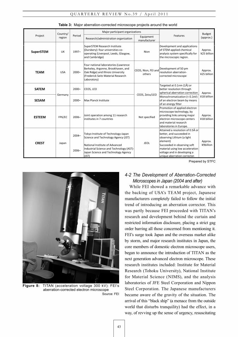
4-1 Global Trend of Aberration Correction Projects Major projects deployed in the world for the development of aberration-corrected microscopes are summarized in Table 3. The following is an overview of each of these projects.- SuperSTEM (UK) The UK has been the leader when it comes to the type of transmission electron microscope that scans converged electron beams (STEM), both in terms of theoretical basis and practical development. It is now advancing the SuperSTEM project, aiming at a further performance upgrade of STEM. The system uses a high-luminance, high-interference electron beam converged to a diameter of 0.1 nm or less by means of aberration correction lenses, and is tagged
4

42
S C I E N C E & T E C H N O L O G Y T R E N D S
as “A Synchrotron in a Microscope” because it is associated with the synchrotron radiation facilities that have shown remarkable progress in recent years. SuperSTEM is one of the earliest starters among the projects related to aberration correction around the world.- TEAM (USA) The USA launched the TEAM (Transmission Electron Aberration-corrected Microscope) project in 2000 under the initiative of the Department of Energy (DOE), and started moves in view of gaining the lead in equipment development, while constructing a wide installation base of aberration-corrected microscopes among the major national laboratories.[3] The project tried to establish a closer link with such manufacturers as FEI, JEOL, and Hitachi (the latter two have bases in the USA), and purchased state-of-the-art equipment on an as-needed basis. The TEAM project especially provided the driving force behind the surge of FEI.- SATEM/SESAM (Germany) Germany launched two projects, starting around 2000, whose activities were centered in CEOS (the company that developed the aberration corrector) and LEO (a national policy concern). One of the projects is called SATEM (Sub-Ångstrom-TEM) and is aimed at developing high-resolution electron microscopes, and the other, SESAM (Sub-Electronvolt and Sub-Ångstrom Microscope), aims at the development of higher resolution spectroscopic measurement as well as electron microscopes. - ESTEEM (EU) In 2006, EU countries launched ESTEEM (Enabling Science and Technology for European Electron Microscopy) as a countermeasure to USA’s TEAM, and started the development of element technologies in close cooperation among EU countries.19] As the project name indicates, its major objective goes beyond developing equipment technology, and holds in view a germination and deployment of new science.In this regard, the project places emphasis on constructing the network that connects researchers. Amid the global unfolding of electron microscope projects triggered by the actual realization of the aberration corrector, a move that deserved special attention was the full-fledged entry of the USA into this area with an unprecedented investment, which came as a considerable shock to those involved in this area in Japan. The USA had long been sitting on the sidelines in regard to electron microscope
development. As described earlier, the launch of a nanotechnology initiative served as a backdrop to the USA’s TEAM project. When President Clinton, the incumbent at the time, advocated the promotion of nanotechnology, he quoted Dr. Feynman’s now-famous 1959 lecture, “Plenty of room at the bottom,”[20] in which Dr. Feynman clearly pointed out the importance of the electron microscope. This likely served as the catalyst for the launch of the TEAM project. In comparison with ultra-high voltage electron microscopes, which normally required several billion yen per installation, aberration-corrected microscopes are much more cost effective, requiring around 300 to 600 million yen per installation. The total cost was around 2 billion yen per installation, which is a relatively low price tag for a project managed under the initiative of the government. Therefore, a relatively good overall return on investment was expected. Amid the surge of demand, FEI was very quick to introduce an aberration corrector and strengthen its level of base technology and the productivity of electron microscopes, triggering a drastic realignment of the world market, which had almost been the exclusive territory of Japanese manufacturers. FEI was once an electron microscope business unit of the general electric giant Philips (the Netherlands). When separated from Philips, the business unit purchased the ion beam company FEI (USA) to attain technological independence. When it was still a business unit of Philips, the engineers were mainly engaged in the development of electron microscopes with an emphasis on general versatility, and they did not embark on the development of high performance instruments that might threaten Japanese manufactures. Once unfettered by the general product giant, the engineers at FEI grabbed the opportunity to pursue high performance without restraint and to manufacture an aberration-corrected microscope. This is another example of a venturing spirit that worked in favor of the business. The fl agship equipment thus produced by FEI, named “TITAN” (Figure 8), enjoyed the utmost admiration from around the world and occupied a dominant position in the TEAM project. TITAN steadily increased its installation base in major research institutes of the world, replacing the Japanese counterpart one by one.
Q U A R T E R L Y R E V I E W N o . 3 9 / A p r i l 2 0 1 1
43
4-2 The Development of Aberration-Corrected Microscopes in Japan (2004 and after)
While FEI showed a remarkable advance with the backing of USA’s TEAM project, Japanese manufacturers completely failed to follow the initial trend of introducing an aberration corrector. This was partly because FEI proceeded with TITAN’s research and development behind the curtain and restricted information disclosure, placing a strict gag order barring all those concerned from mentioning it. FEI’s surge took Japan and the overseas market alike by storm, and major research institutes in Japan, the core members of domestic electron microscope users, began to announce the introduction of TITAN as the next generation advanced electron microscope. These research institutes included: Institute for Material Research (Tohoku University), National Institute for Material Science (NIMS), and the analysis laboratories of JFE Steel Corporation and Nippon Steel Corporation. The Japanese manufacturers became aware of the gravity of the situation. The arrival of this “black ship” (a menace from the outside world that disturbs tranquility) had the effect, in a way, of revving up the sense of urgency, resuscitating
+��<�"�������4�
������+�����
�<���-����"�-����������0������
=��������������
�--��3��������"#���)������������������0�����
�8��-)����
)���6�"�����
� ��� � # > ��� � ! , � � ,� ��
�������� ?; ..'@
��-����� �������"#�>���������
!���*��4�A�6�������5���������"�2
�-��������B�5��-��, �B���� �C,����1 �
������)*������
&���
!�5�,�-)���������--,�"�������
�6���� 2�--,����"#�)�"�,�
���,4�����4���)��-�"�6�"�,,4�6���
�#��)�"���"�-�"��������
�--��3�
D�(�*�,,���
=�����������,�,�*����������B�1���"��
���� ?�� ����@
�� �� � � �*� ��� �� � � "�
�����,�4 �������� ������#�5�� �����
:��������������>,,������?��5�����4�
=������"������0� ������,�������"#�
B�*������4�
��:� �&��� �=�>�����
��#���
!�5�,�-)�����6�(��-)�
����,�������*��������2
"����"����)�"���"�-�
�--��3��
D�(�*�,,���
���������������)�E�����
�����
C��)��4
����@ ��:� �B�:
��:� �$�����B�:
� �
*����������,�������#����#�
�-#���"�,��*���������"����"���� �--��3��
D9�*�,,���
����� ����@ �3�+,��"��>��������
���"#��)���0������F��������
�6�����,�"�����*��)�*4�)�����
�6���������4�6�,���
6 , � ,
������ =+7��� ���7@G������-���������)�����������"#�
��������������'�"��������&����-�"�6���
+��)�������6��--,�����,�"�����
)�"���"�-����"#��,��4 �*4�
-��5������,������)����)�<���
�,�"�����)�"���"�-��"�������
����)������,�������"#�
,�*�����������������-��
�--��3��
D9�*�,,���
-
!��� G�-��
���/@���4��>����������6���"#��,��42G�-���
�"���"��������"#��,��4�����"4�G����
G�:B
���������������,�������6���(E����
*����� �������""���������
�*���5����B��#��)���,��#��
�,�)���� �--��3�
D.*�,,����&������,�>����������6���5��"���
> � � � , � � � � # , ����
��""����������*���5������6��
� � , � , , �����7@
>��������,��"���"��������"#��,��4�����2
G�-����"���"��������"#��,��4�����"4�
G����
)������,�������,�1��""�,��������
5�,��������������5�,�-������
���8����*���������"����"����
Prepared by STFC
Table 3: Major aberration-corrected microscope projects around the world
Source: FEI
Figure 8: TITAN (acceleration voltage 300 kV): FEI’s aberration-corrected electron microscope

44
S C I E N C E & T E C H N O L O G Y T R E N D S
the enthusiasm with a view toward reaching the top of the world again. Although Japan slightly lagged behind initially, a project dedicated to the development of the aberration corrector was launched with the least delay, before the problem got out of hand, under the support of Japan Science and Technology Agency (JST) (see Table 3). JEOL, which inherently had a high level of base technology, manufactured a series of independently designed aberration correctors in a row within a short time span, and succeeded in leaping onto the top of the resolution competition.21] In Figure 1, the point indicating the highest resolution in the world at the present time, labeled as “CREST,” represents the outcome of the support from JST. Yet another achievement of CREST (Core Research of Evolutional Science & Technology) worthy of special note was the successful development of a new type of aberration correction lens, which went further than simply following-up the preceding technology and incorporated independent ideas.[22] Although based on the Rose-type configuration that uses transfer lenses, it has another hexapole lens added to the conventional two-stage configuration. By arranging these three-stage hexapole lenses at meticulously-balanced rotational angles, it proved that six-fold symmetry astigmatism could be eliminated (Table 2: 2009). This idea made further progress toward perfecting aberration correction lens characteristics. The outcome was valued very highly throughout the world, and it helped promote Japan’s high standard of base technology for the electron microscope. As the next step, the technology development for chromatic aberration correction is now underway at CREST. CEOS is also developing this technology.[23] Researchers at CREST are pressing forward with this research and development so as not to be left in the dust of CEOS again. The development of a high performance aberration-corrected microscope attained success as the outcome of a Japanese project, and it made up suffi ciently for the damage caused by the late start. Looking back on the excitement and frenzy around the arrival of the aberration corrector calmly again, however, we have to face up to the fact that even FEI was completely dependent on CEOS in terms of the aberration correction lens itself. This situation is also true for many of the commercial instruments manufactured in Japan. We have to remember that CEOS still holds the decisive vote on the whole process of development.
As will be described in the next chapter, a trend is becoming more pronounced as the performance and multifunctionality of the electron microscope are upgraded, that is, as the importance of peripheral and auxiliary equipment increases relative to that of the microscope itself.
How to Proceed from Here—Trend toward Multifunctionality and Purpose-Specificity in Advanced Electron Microscopes
The modern electron microscope is not simply a magnifi cation vehicle used to see atoms.[24] It is a total measuring instrument that can provide three major elements of metrology (diffractometry, spectroscopy, and microscopy) in a single piece of equipment, and can make a series of measurements on the same, tiny volume within a sample (Figure 9).[25] As the modern synchrotron radiation facility, as represented by SPring-8, has separate beam lines depending on the objectives (e.g. purpose of measurement, and types of samples), an increasing amount of advanced electron microscope equipment is designed with an emphasis on a particular method, to bring out maximum performance for a particular objective. With this trend in mind, the author outlines the future development of the electron microscope, from each viewpoint of technical development and applied research.
5-1 Evolution of Technology: Peripheral Devices Inclusive
As mentioned in the previous section, the arrival of the aberration correction lens brought about an inversion of the subordinate-superior relationship: a portion of the lens, conventionally considered a part contained in the main body of the microscope, became peripheral equipment and bears greater importance than the main body of the microscope. This trend, in fact, was showing a sign of unfolding even before the arrival of the aberration corrector. For example, the spectrometers for measuring characteristic X-ray and electron energy have been peripheral units provided by manufactures specializing in the area to electron microscope manufacturers. Therefore, for users that attach importance to spectroscopic performance, the selection of the microscope itself was of secondary priority. As the majority of spectrometers are the products of overseas manufacturers, Japanese electron
5

Q U A R T E R L Y R E V I E W N o . 3 9 / A p r i l 2 0 1 1
45
microscope manufacturers were gradually losing the lead in the peripheral market as well. Gatan (USA), an electron energy spectrometer manufacturer enjoying a near monopoly of the global market, upgraded its line of products in synchronization with the arrival of the aberration correction lens, and has successfully secured a certain number of users in the world market, as it had before. Today, the trend (i.e. the electron microscope itself has only secondary importance) is in the process of becoming increasingly pronounced. FEI (USA) has achieved the growth we see today, by enhancing its partnership with such companies as GEOS and Gatan. With the arrival of the aberration corrector, and also with the higher performance of associated peripheral devices, the electron microscope itself is being pressed hard for higher sophistication. The measures to be taken by the Japanese manufacturers would be the following two: 1) further sophistication of the electron microscope itself, and at the same time, 2) starting the development of Japanese high-performance spectroscopes. These are included among the objectives of the MEXT (Ministry of Education, Culture, Sports, Science and Technology)
project titled the Development of Next Generation Element Technology for Electron Microscopes, which started in 2006. The themes adopted in the project include the development of a Japanese high-resolution characteristic X-ray spectrometer, as well as other fundamental element technologies, such as the electron gun and storage media. The theme has so far been well on course. However, considering the fact that the technologies related to the electron microscope and peripherals have become so broadly diversified (Figure 9), no single project is able to cover all the aspects. Continued, uninterrupted measures should be taken from now onward as well. Of particular note is the fact that no project is underway with the aim of commercial realization for the development of the electron energy spectrometer, one of the most important technology aspects. Gatan has already attained a very high potential, and there is no need to set up an excessive competition that might damage relations with it. Still, the development of Japanese equipment should be started based on mid- and long-term perspectives. The aberration corrector has had ramifications beyond the upgrade of the maximum attainable
� !" (��#��##����� ������)����#����
#� !" !�������(��#��##����� ������
)����#����
������������������
��������� �
• �����4����-�������H2��4����,4�����!H�
• %��#�����,������H2��4��-�"����"�-4�H���
• �,�"����������42,�����-�"����"�-4���B��
• ���)�"�����,�������)����)�,��-,��1�5��
�����6����"��
• %��54����)�������6�"���������)�"��)����
$2"���������)����
• B�����0��,�"�����)�"���"�-�
• �,�"�����*��)�#�,����-#4
• �!���)����-#4
+ � � � � , , � * 6 ���!
����������������
�������������
• ��)-��������"�����,
• +��0�2���5�����2��-�#�-��*���� �"#���"�,�-��-������ �
"����"���"� )������)��� ��"�• +��"����������"����,����,4����*4�)������6����!�
"��5������*��)��,�"�������66��"�����
• +��"��������,�"�������66��"����
• !�66��"������)�����
"����"���"��)������)��� ���"�
• ��)������,�������*���5�����
• ��)��-#����"�����,,����*���5�����
Prepared by STFCFigure 9: Future evolution of advanced electron microscopy: toward multifunctionality and versatility

46
S C I E N C E & T E C H N O L O G Y T R E N D S
resolution. First of all, the chances of in-situ observation becoming possible have become markedly greater. Due to the structural requirements of the objective lens, the sample must be placed inside the lens (Table 1). In conventional electron microscopes, the atomic level of resolution was realized (or, spherical aberration was suppressed as low as possible), only at the penalty (minimization) of the space allowed for the sample. After the arrival of aberration correction technology, the sample space design with size expanded to several centimeters became feasible (as compared to several millimeters before) with the atomic resolution maintained. This enabled the use of sample holders with complicated geometry for in-situ observation. The insertion of such sample holders was almost impossible before. Outstanding attempts in recent years include the microscope and sample holder specifically designed for in-situ observation of catalytic action under native atmosphere. Projects have started for promoting this research in Japan and overseas, now creating a technical area called the “variable pressure/environmental electron microscope.” Another major trend is to pave the way to the non-destructive observation of soft organic and biological samples. As these samples suffer considerable damage even when used in electron microscopes that use an acceleration voltage between 100 and 200 kV, a drastic reduction of acceleration voltage and high resolution observation must be simultaneously realized in a conventional transmission electron microscope. Nion developed a 60 kV electron microscope, and has recently succeeded in an atomic identifi cation analysis of a mono-atomic layer material consisting of boron and nitrogen (a graphene (carbon)-like structure). The outcome has had a huge impact and was the cover story of Nature.[26] In Japan, the researchers at AIST (National Institute of Advanced Industrial Science and Technology) have been carrying out a detailed analysis of carbon material using a 30–60 kV electron microscope developed by CREST,[27] taking the lead ahead of the rest of the world in this area. Let us take a brief look at the ultra-high voltage electron microscope. Although its territory has shrunk as compared with the time before aberration correction, there is no room for doubt that some observation techniques absolutely require the ultra-high voltage specifi cations. Theses instances include, for example, the observation of thick (near bulk state)
specimens of inorganic or biological systems, and the physics of various measuring methods whose characteristics depend on acceleration voltage. The ultra-high voltage electron microscope is technology that Japan has established through persistent efforts, and it is worthy of pride. From the viewpoint of the succession of technology, it would not be wise to abandon the ultra-high voltage electron microscope totally because of the arrival of aberration correction. At present, the upgrading of ultra-high voltage microscopes is underway at a rapid pace at their installation sites in major universities and research institutes, and the objective of which is to incorporate purpose-specifi c design. Although this report does not cover the introduction of all the relevant technologies, the global trend of advanced electron microscopes, since the arrival of aberration correction, is rapidly progressing toward multifunctionality and versatility as has been mentioned. This is an important period for researchers and engineers to be geared toward producing their independent ideas, and they have to constantly keep abreast of world trends so as not to be left behind. Commercial, all-purpose electron microscopes that are constructed by integrating existing technologies and are better than the average products may be widely available in the market, but an even more important point to keep in mind regarding future equipment development is the significance of unique design specialized for a particular purpose and particular object of observation. Researchers, in particular, are expected to develop their own ideas, and, by implementing them in the latest instruments, lead the world.
5-2 Evolution of Basic and Applied Research Using the Aberration-Corrected Microscope
In the history of science, there have been many instances where a breakthrough enhancement in measurement performance brought us new scientific knowledge. It has been more than ten years since the development of the aberration correction lens, and now that its technology is almost established, the current global trend in this area is to step forward into a new phase where the state-of-the-art electron microscope, with its high performance and versatility, is used in the quest for a new evolution in nano- and bio-research. As mentioned earlier, ESTEEM (joint undertaking of EU countries) is a project established

Q U A R T E R L Y R E V I E W N o . 3 9 / A p r i l 2 0 1 1
47
based on this viewpoint. TEAM project (USA) brought its role to an end in 2010, and the emphasis has shifted to the upgrade and expansion of the network for collaborative use, in view of broadening the community of microscope users. This trend indicates that the aberration correction technology as applied to electron microscopes has had the effect of expanding the community of average users owing to the enhanced versatility, as well as of meeting the requirements from highly specialized, purpose-specific users. Japan should not miss this trend. The creation of opportunities to discover potential applications in such fi elds as nano- and bio-technology will be required, as well as a continued effort by specialists in the field to lay a firm foundation. This move will also help Japan put its revived specialty on a fi rmer basis.
5-2-1 Development of Applications: Expansion of User Community Optical adjustment in the aberration-corrected electron microscope is carried out automatically by a computer, eliminating the need for craftsmanship, which was an indispensable prerequisite for viewing atomic images. This made the operation of an electron microscope much easier and accessible to a non-specialist, at least technically. Aberration correction also brought about a 10 to 100 times enhancement of electron beam luminance, dramatically improving the efficiency of analysis. In fact, a measurement that might have required a day’s work can be done in a time span as small as several minutes, providing a huge benefit. As typically exemplified by these advantages, pre-aberration correction high performance electron microscopes were instruments only for highly skilled specialists, but aberration correction technology helped expand accessibility to more general users as a conventional instrument. It is therefore noteworthy that many research organizations in the private sector pressed ahead with the introduction of aberration-corrected microscopes before universities and national research institutes. Maturing as a general purpose instrument with an expanding user community represents a situation where the use of advanced electron microscopes becomes widespread, and there will be ever increasing cases of electron microscopic analysis in the research areas where the instrument has scarcely been used before. This translates into a huge opportunity for
researchers in any fi eld to make a new discovery. Dr. Iijima’s case is a prime example of this situation: the carbon nanotube, which became synonymous with nanotechnology, was only found because he was working in the environment where he always had an electron microscope at his disposal. As a system for collaborative use, the Nanotechnology Researchers Network,[28] established under the initiative of MEXT before the existence of the aberration corrector, has been continuing its effort to promote a wider use of aberration-corrected microscopes. In recent years, a good number of aberration-corrected microscopes are being put in place in the outsourcing analysis centers in the private sector as well.
5-2-2 Basic Research: Construction of an Expert Network Since the development of aberration correction, the elect ron microscope has evolved into a multifunctional, multifaceted platform. To make the most of this instrument and to promote the chances of new discovery, the cultivation of a better understanding of the basics of each specialized field is a challenge of the utmost importance. For example, with an aberration correction lens, the electron beam can be squeezed down to a narrow diameter of 50 pm or less, near the limit of quantum mechanics. How does the electron propagate inside the sample when a beam this narrow impinges it? Can we understand the phenomena taking place within a sample (elastic scattering, non-elastic scattering, and emission of characteristic X-rays) as an extension of conventional electron scattering theory? These questions will probably arise in every aspect. The key to leading the next generation of global nanotechnology study is theoretical and experimental research into, and verification of the fundamentals of each of these phenomena that are not yet contained in a textbook. Without a correct understanding of what they see, researchers are likely to overlook a new discovery upon coming across it. Only researchers with a keen eye and correct understanding will encounter serendipity. The fundamental research of today is so broadly diversifi ed and segmentalized that no single researcher can cover it all. Even the items listed in Figure 9 may not be exhaustive. They may only be a partial list of research fi elds that happened to come to the author’s mind. There are many researchers engaged in the

48
S C I E N C E & T E C H N O L O G Y T R E N D S
electron microscope, as it is designated as Japan’s specialty. Now is the time to build an all-Japan framework that includes research hubs established for each professional discipline at each university and research institute based on the specialty of the organization and that provides cross-cutting, organized links connecting these hubs. To make full use of researchers’ capabilities, extensive use of a network of personal contacts, as well as an instrument network, is also essential because sharing expert knowledge and information—they often have a deep-rooted common base—will help construct novel ideas that are ahead of the rest of the world. Conceptually, the organizing principle of ESTEEM (EU countries) may be more suited to Japan rather than that of TEAM (USA). Under the all-Japan framework, each hub would pursue a one-and-only design based on its specialty in cooperation with domestic electron microscope manufacturers. The technical know-how obtained through this process may lead to the development of new equipment enabling the heretofore inaccessible observation of nano-scale samples. These new instruments will attract the attention of the new-user community, immediately providing high expectations for further expansion of the support network. As pioneering research in this area, a priority study (Grant-in-Aid for Scientifi c Research on Priority Areas) has started.[29]
Summarizing the discussion of this section, the following two points are of critical importance when we consider how to proceed from here with the electron microscope: 1) the expansion of the user community (spread of general purpose instruments), and 2) the cultivation of specialized techniques (introduction of purpose-specifi c instruments). These two concepts may appear contradictory when viewed from the standpoint of equipment development, but they are not mutually exclusive. Should a mountain be great, it must have both a wide-spread foundation and a soaring peak. Basic research has the effect of raising the peak even higher, and it naturally leads to the development of new equipment that helps widen the community of users. In discussions on the future of electron microscopes, the phrases “general versatility” and “specialized expertise” are often used in a confusing manner. In trying to determine the direction we should take from here, we should always be mindful to organize our thinking.
Conclusion
In the latter half of the 1990s, the arrival of the aberration correction lens brought about a breakthrough upgrade of electron microscope performance and triggered a revolution. This revolution came to international attention against the backdrop of nanotechnology. Even the USA embarked on the development of this technology, as did Germany, the birthplace of the technology. Japan, which had enjoyed a good reputation regarding its specialty of electron microscopes, was highly alarmed by this turn of events. Although Japanese manufacturers were late starters, their inherent high level of technology enabled them to develop high-performance instruments, owing to the research project conducted in cooperation with universities and public research organizations. Today, after more than ten years since the invention of aberration correction, Japanese manufacturers have attained a level that can be rated on par with the fi nest in the world. The world market is, following a period of turbulence caused by a hectic offensive from FEI (USA), gradually calming down and heading toward recovery. Looking back on the history of elect ron microscopes, Japan, a late starter, gradually overtook the precursor (Germany, the inventor) by mustering all its technological power, and fi nally made electron microscopes its specialty. If we take a calm look at the events that took place in the early stage of aberration corrector development, it is apparent that history repeated itself. That is, both the electron microscope and aberration correction lens were invented by overseas researchers. Especially in regard to the aberration corrector, we have to renew our awareness that it was the fruit of 50 years of persistent basic research undertaken in Germany and the UK. Now that Japan has established its reputation as one of the most technically advanced countries in the world, we hear no ridicule that Japanese technology is mimicry. Japan should go further, beyond a short-term development of existing technology into a new era of true discovery and invention from the viewpoint of creating new things from scratch. For this to be realized, we need a system that provides support continuously and doggedly to basic science from medium- and long-term perspectives. Judging the value of research only from the return-on-investment
6
Q U A R T E R L Y R E V I E W N o . 3 9 / A p r i l 2 0 1 1
49
[1] D. A. Muller, “Structure and bonding at the atomic scale by scanning transmission electron microscopy,” Nature Materials, 8 (2009) 263
[2] M. Haider et al., “Electron microscopy image enhanced,” Nature 392 (1998) 768[3] TEAM project (USA) Web site: http://ncem.lbl.gov/TEAM-project/[4] brewbooks, “Electron Microscope Deutsches Museum,” http://www.flickr.com/photos/93452909@
N00/176059674/, (permission for use: Creative Commons Attribution-ShareAlike 2.0 Generic (http://creativecommons.org/licenses/by-sa/2.0))
[5] Kentaro Asakura, Koichi Adachi, “The creators pioneers of the electron microscope,” Igaku Shuppan Center, Tokyo 1989
[6] O.Scherzer, “The theoretical resolution limit of the electron microscope,” Journal of Applied Physics 20 (1949) 20
[7] Hidetaka Sawada, Ko Sanmiya, Shio Fumio Hosokawa, “Spherical aberration corrected TEM and STEM,” Ceramics, 40 (2005) 908
[8] Shigeo Okayama, “Practical realization of aberration correction technology by multipole lenses,” Applied Physics, 76 (2007) 1142
[9] Shigeo Okayama, “Aberration-corrected electron microscopy,” Microscope, 45 (2010) 119[10] O. L. Krivanek et al., “Towards sub-Å electron beams,” Ultramicroscopy 78 (1999) 1[11] N.Dellby et al., “Optimized quadrupole-octupole C3/C5 corrector for STEM,” CPO-7 proceedings, p.97 (2006)[12] J. Zach and M. Haider, “Aberration correction in a low voltage SEM by a multipole corrector,” Nuclear
Instruments and Methods in Physics Research A363 (1995) 316[13] H. Rose, “Outline of a spherically corrected semiaplanatic medium-voltage transmission electron microscope,”
Optik 85 (1990) 19[14] Ceos Web site: http://www.ceos-gmbh.de/[15] Nion Web site: http://www.nion.com/index.html[16] S. Okayama, “A new type of quadrupole correction lens for electron-beam lithography,” Nuclear Instruments
and Methods in Physics Research A298 (1990) 488[17] “Development of the next generation ultra-electron microscope” project (1996–2001):
http://www.jsps.go.jp/j-rftf/saishu_hyouka_08/04_sougou/p_pdf/s_09.pdf[18] SuperSTEM project (UK) Web site: http://www.superstem.com/[19] ESTEEM project (EU) Web site: http://esteem.ua.ac.be/[20] Keynote speech by R. P. Feynman (American Institute of Physics, 1959): “There’s plenty of room at the
bottom,” http://www.zyvex.com/nanotech/feynman.html[21] H. Sawada et al., “STEM imaging of 47 pm-separated atomic columns by a spherical aberration-corrected
electron microscope with a 300-kV cold fi eld emission gun,” Journal of Electron Microscopy 58 (2009) 357.[22] H. Sawada et al., “Correction of higher order geometrical aberration by triple 3-fold astigmatism fi eld,” Journal
of Electron Microscopy 58 (2009) 341
References
or pay-per-performance point of view always carries the risk of missing out on a huge outcome in the future. Japan has to learn from these experiences. A variety of measuring techniques now unfolding around the aberration-corrected electron microscope will surely present a breeding ground for breakthrough discoveries and inventions in the near future. In order to dispatch a brand-new technology from Japan to the world in the future, it is an urgent task to construct a framework in which the enhanced networking among
the researchers is of special importance. The cross-sectional power base will be strengthened through open-minded discussion among researchers in many specialized fi elds.
Acknowledgement During the preparation of this report, Professor Yuichi Isohara Ikuhara (Tokyo University) provided me with useful advice and comments. I am sincerely grateful to him.

50
S C I E N C E & T E C H N O L O G Y T R E N D S
[23] B. Kabius et al., “First application of Cc-corrected imaging for high-resolution and energy-filtered TEM,” Journal of Electron Microscopy 58 (2009) 147
[24] Special Issue, “What can we do now with the electron beam?” Journal of the Crystallographic Society of Japan, 47 No. 1 (2005) 2
[25] Eiji Abe, “Evaluation of local structure/composition using an advanced electron microscope,” OYO BUTURI, 79 (2010) 293
[26] O. L. Krivanek et al., “Atom-by-atom structural and chemical analysis by annular dark-field electron microscopy,” Nature 464 (2010) 571
[27] K. Suenaga et al., “Visualizing and identifying single atoms using electron energy-loss spectroscopy with low accelerating voltage,” Nature Chemistry 1 (2009) 415
[28] MEXT, Nano Technology Network Center: http://www.nanonet.go.jp/japanese/[29] MEXT, Grant-in-Aid for Scientifi c Research on Priority Areas, “Nano material science of functional element”:
http://nanodopant.com/http://www.t.u-tokyo.ac.jp/tpage/index.html
Eiji ABEAffi liated Fellow, NISTEPAssociate professor at Tokyo University (graduate school, engineering)He joined the faculty of Tokyo University after his research work at National Institute of Material Science. In 2002, he became an affi liated fellow at the Oak Ridge National Laboratory. His interest in the electron microscope began in his graduate years, and he is now a leading researcher in subjects including qausicrystals and other complex structured materials. His motto is, “The most important quality in research is enthusiasm.”
(Original Japanese version: published in November 2010)
Profi le