Embed Size (px)
Citation preview

NAME:
GEORGIA INSTITUTE OF TECHNOLOGY School of Electrical and Computer Engineering
ECE 4430 Second Exam Closed Book and Notes Fall 2002 October 30, 2002 General Instructions: 1. Write on one side of the paper. (1 Pt.) 2. Put answers to all questions in the spaces provided on the test. (1 Pt.) 3. Show all work for full credit on questions requiring calculations. No credit will be given for answers
alone, without supporting work. 4. Problems and questions are weighted as indicated. The maximum score is 100 points. 5. If you need more paper (provided in class), remove the staple from the exam and, when finished,
arrange the test in order. Place the extra pages with supporting work in the test behind the page where the problem appears and indicate accordingly. Staple the entire test together so that there are no loose pages. (1 Pt.)
TEST SCORE: / 100
I certify that I have neither given nor received any assistance while taking this test from anyone. (Signature) (1 Pt.) .Place a check mark in the box if you observed any suspicious actions while taking this test ٱ

2
Formula Sheet: Equations/Constants that you may, or may not, need are listed below:
K’ = 50 µA/V2 (unless otherwise stated in the problem) Kn = K’W/L λ = 0.01 V-1 (unless otherwise stated in the problem) VTO = 0.7 V (unless otherwise stated in the problem) γ = 0.5 V1/2 (unless otherwise stated in the problem) 2φF = 0.6 V (unless otherwise stated in the problem) ID-Triode = (Kn/2) [2(VGS – VTN)VDS - VDS
2] ID-Sat = (Kn/2) (VGS – VTN)2 (1 + λVDS) VTN = VTO + γ [sqrt(2φF – VBS) – sqrt(2φF)] ro-MOS ≈ 1 / (λIDS) gm-MOS = sqrt[2IDSKn] Vds-sat = sqrt(2IDS/Kn) gmb-MOS = ηgm-MOS η = γ ÷ 2 sqrt(2φF – VBS) Vt = kT/q ≈ 26 mV and IS = 1E-15 A (unless otherwise stated in the problem) IDiode = IS [exp(VD/Vt) – 1]
Cj = Cj0
1 -
vDψo
m 0.33 ≤ m ≤ 0.5
VA = 100 V (unless otherwise stated in the problem) βF = 50 (unless otherwise stated in the problem) ICE = IS [exp(VBE/Vt) – 1] [1 + VCE/VA] ro-NPN = VA / ICE gm-NPN = ICE/Vt CMRR = |Adm| / |Acm| Zmiller-in = Z / (1 - k) Zmiller-out = Z k / (k – 1)

3
Fabrication – Part A (30 Points)
1. Draw the schematic (label the terminals) and identify the devices of the figures shown below, as they
would be used (be specific – base-emitter diode of lateral NPN, accumulation-mode MOS capacitor,
etc.). (10 pts)

4
2. Use the layout shown below to answer the following questions.
(a) Draw the corresponding schematic. ( 5 pts)

5
(b) Which terminal(s) (1, 2, 3, 4, or 5) is(are) more than likely connected to the positive power supply?
(2 pts)
Why?
(2 pts)
(c) Which terminal(s) is(are) more than likely connected to the negative power supply?
(2 pts)
Why?
(2 pts)
(d) Which terminal(s) is(are) more than likely the input(s) of the circuit?
(2 pts)
(e) What specific capacitor components (e.g., Cdb_sidewall, Cdb_bottom, Cgs_overlap, Cgs_saturation, etc.) do you
expect to be present on terminal 5? (5 pts)

6
Single and Two Transistor Amplifiers – Part B (25 Points)
1. Circle the single transistor amplifiers that produce a non-inverting transfer function. (6 pts)
CC CB CE CD CG CS
2. For the circuit shown and using small signal parameters (e.g., rπ, gm, β, etc.), (a) derive input
resistance rin and the transfer function from Vi to Vo1 (i.e., Vo1/Vi) –assume VA is infinite (ro is infinite).
Vcc
RE
RC
Vi
Vo1
Vo2
rin
q n1
q n2
rx
(10 pts)
(b) The gain from Vi to Vo2 (i.e., Vo2/Vi) is greater than / less than / equal to Vo1/Vi. (2 pts)
(c) True / False: Vo1 is in phase with Vo2. (2 pts)
(d) Derive the resistance looking into the collector of qn1 (rx)? (5 pts)
7
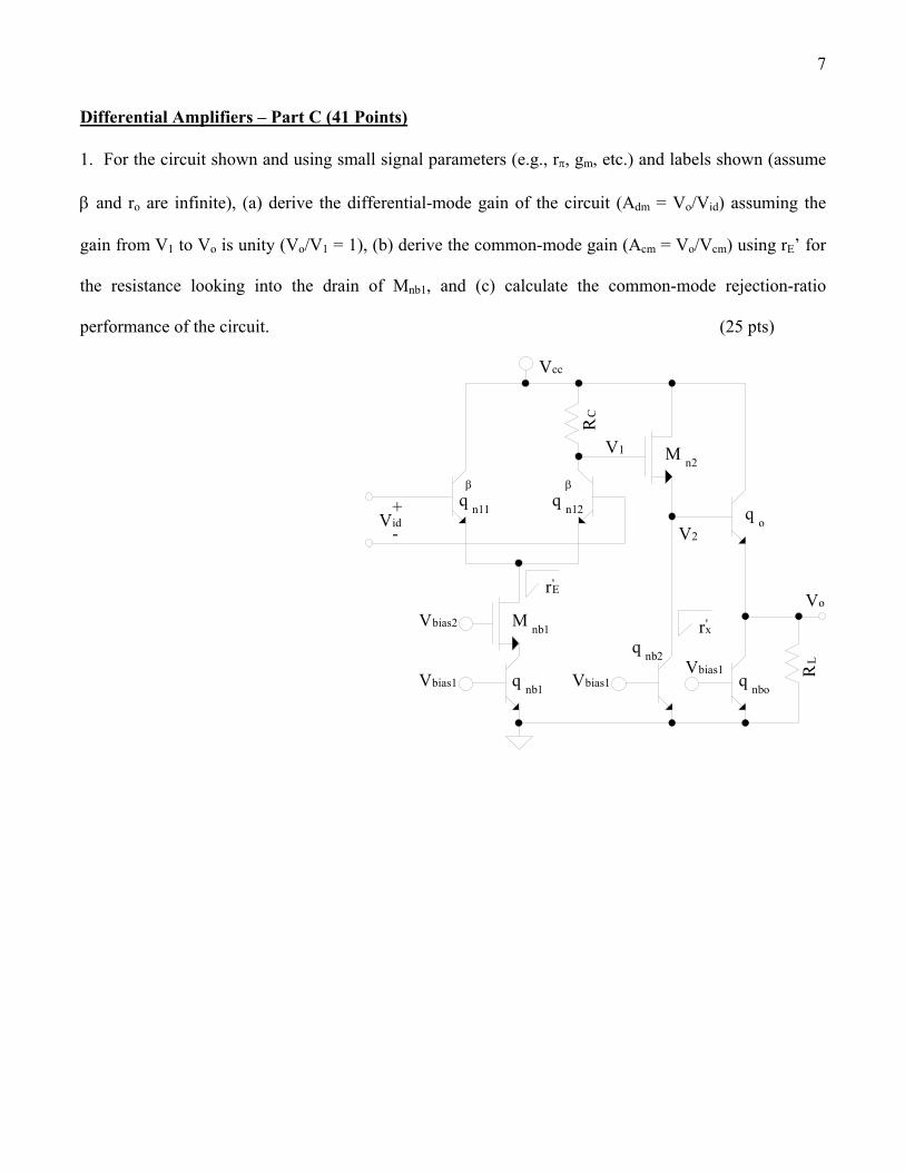
Differential Amplifiers – Part C (41 Points)
1. For the circuit shown and using small signal parameters (e.g., rπ, gm, etc.) and labels shown (assume
β and ro are infinite), (a) derive the differential-mode gain of the circuit (Adm = Vo/Vid) assuming the
gain from V1 to Vo is unity (Vo/V1 = 1), (b) derive the common-mode gain (Acm = Vo/Vcm) using rE’ for
the resistance looking into the drain of Mnb1, and (c) calculate the common-mode rejection-ratio
performance of the circuit. (25 pts)
rE'
RL
RC
Vcc
Vbias2
q n11 q n12
Vo
Vid+-
β β
Vbias1 Vbias1Vbias1
q o
M n2V1
V2
q nb1
q nb2
q nbo
M nb1 rx'
8
rE'
RL
RC
Vcc
Vbias2
q n11 q n12
Vo
V1
V2
Vid+-
β β
Vbias1 Vbias1Vbias1
q o
M n2V1
V2
q nb1
q nb2
q nbo
M nb1 rx'
2. Which devices have been used as current sources or sinks? (6 pts)
3. Of those, which one(s) exhibit(s) the lowest Vmin? (6 pts)
4. Which one(s) has(ve) the best output resistance performance? (4 pts)


10
11

12