Embed Size (px)
Citation preview

University of South FloridaScholar Commons
Graduate Theses and Dissertations Graduate School
6-20-2007
Gate Level Dynamic Energy Estimation InAsynchronous Circuits Using Petri NetsRyan MabryUniversity of South Florida
Follow this and additional works at: http://scholarcommons.usf.edu/etd
Part of the American Studies Commons, and the Computer Engineering Commons
This Thesis is brought to you for free and open access by the Graduate School at Scholar Commons. It has been accepted for inclusion in GraduateTheses and Dissertations by an authorized administrator of Scholar Commons. For more information, please contact [email protected].
Scholar Commons CitationMabry, Ryan, "Gate Level Dynamic Energy Estimation In Asynchronous Circuits Using Petri Nets" (2007). Graduate Theses andDissertations.http://scholarcommons.usf.edu/etd/3826

Gate Level Dynamic Energy Estimation In Asynchronous
Circuits Using Petri Nets
by
Ryan Mabry
A thesis submitted in partial fulfillment of the requirements for the degree of
Master of Science in Computer Engineering Department of Computer Science and Engineering
College of Engineering University of South Florida
Co-Major Professor: Nagarajan Ranganathan, Ph.D. Co-Major Professor: Hao Zheng, Ph.D.
Srinivas Katkoori, Ph.D.
Date of Approval: June 20, 2007
Keywords: Simulation, Power, Handshaking, Modeling, CPN Tools
© Copyright 2007, Ryan Mabry

ACKNOWLEDGEMENTS
I would like to thank Dr. Ranganathan and Dr. Zheng for directing and
helping me throughout this thesis. I am also thankful for the help provided by
Narender Hanchate, Ashok Murugavel, and Soumyaroop Roy. I would also like to
thank my family for the support and encouragement they have shown.
On the professional level, I would like to thank the many institutions and
people that developed the tools that made this thesis possible. I would like to thank
the University of Manchester and Dr. Steve Furber for the development of their Balsa
asynchronous synthesis tool. I would also like to thank the Virginia Tech VLSI for
Telecommunications group and Dr. Dong Ha for the development of their cell library.
I would also like to thank Dr. Roberto Tamassia and Brown University for the
development of the JDSL library, which this work made extensive use of. I would
also like to thank the CPN group at the University of Aarhus in Denmark for their
development of CPN Tools.

i
TABLE OF CONTENTS LIST OF TABLES iii
LIST OF FIGURES iv
ABSTRACT vi
CHAPTER 1 INTRODUCTION 1 1.1 The Need for Low Power 1 1.2 Power Consumption 3
1.2.1 Static Power Consumption 3 1.2.2 Dynamic Power Consumption 4
1.3 Asynchronous Circuits 5 1.3.1 Asynchronous Communication 5 1.3.2 Asynchronous Circuit Implementation Styles 7
1.4 Motivation 7 1.5 Contributions 8 1.6 Related Work 9
1.6.1 Sequential and Combinational Power Estimation 10 1.6.2 Asynchronous Energy and Power Estimation 15
1.7 Thesis Overview 19 CHAPTER 2 PETRI NET FRAMEWORK 20
2.1 Petri Net Basics 20 2.2 Power Estimation Using Petri Nets 25
CHAPTER 3 PETRI NET MODELING OF ASYNCHRONOUS CIRCUITS FOR ENERGY ESTIMATION 29
3.1 Hierarchical Colored Asynchronous Hardware Petri Nets 29 3.2 HCAHPN Low-Level Modeling 33
3.2.1 Gate Functionality Substructure 34 3.2.1.1 Gate Functionality Firing Example 38
3.2.2 Switching Activity Substructure 45 3.2.2.1 Switching Activity Firing Example 47
3.2.3 Token Filter Substructure 51 3.2.3.1 Token Filter Firing Example 53
3.3 HCAHPN High-Level Modeling 56

ii
CHAPTER 4 A FRAMEWORK FOR ENERGY ESTIMATION 61 4.1 Tool Flow 61 4.2 Energy Estimation Formula 66
CHAPTER 5 EXPERIMENTAL RESULTS 68
CHAPTER 6 CONCLUSION 71
REFERENCES 73

iii
LIST OF TABLES
Table 1.1 ITRS Road-Map, 2006 International Technology Road-Map for Semiconductors 2
Table 4.1 Intrinsic Gate Delays 64
Table 5.1 Simulation Results 68

iv
LIST OF FIGURES Figure 1.1 Asynchronous Communication 5 Figure 1.2 Two-Phase Handshaking 6 Figure 1.3 Four-Phase Handshaking 6 Figure 1.4 Taxonomy Diagram of Power Estimation at Different Levels of
Abstraction in Sequential and Combinational Systems 10
Figure 1.5 Taxonomy Diagram of Energy and Power Estimation Methods in Asynchronous Systems 15
Figure 1.6 Petri Net Representation of Muller C-element 17 Figure 2.1 HCHPN Structure of NAND Gate 26 Figure 2.2 Tool Flow for HCHPN Power Estimation 28 Figure 3.1 AND Gate 33 Figure 3.2 HCAHPN Structure of AND Gate 33 Figure 3.3 Gate Functionality Structure Detail of AND Gate 34 Figure 3.4 Gate Functionality Step 0 38 Figure 3.5 Gate Functionality Step 1 39 Figure 3.6 Gate Functionality Step 2 40 Figure 3.7 Gate Functionality Step 3 41 Figure 3.8 Gate Functionality Step 4 42 Figure 3.9 Gate Functionality Step 5 43 Figure 3.10 Gate Functionality Step 6 44

v
Figure 3.11 Switching Activity Structure Detail of AND Gate 45 Figure 3.12 Switching Activity Step 0 47 Figure 3.13 Switching Activity Step 1 48 Figure 3.14 Switching Activity Step 2 49 Figure 3.15 Switching Activity Step 3 50 Figure 3.16 Token Filter Structure Detail of AND Gate 51 Figure 3.17 Unknown Signal State 52 Figure 3.18 Known Signal State 52 Figure 3.19 Token Filter Step 0 53 Figure 3.20 Token Filter Step 1 54 Figure 3.21 Token Filter Step 2 55 Figure 3.22 Wine Shop Asynchronous Circuit 56 Figure 3.23 Flattened Wine Shop Circuit 57 Figure 3.24 Wine Shop Gate Signal Graph 58 Figure 3.25 Wine Shop Petri Net 59 Figure 3.26 Wine Shop HCAHPN 60 Figure 4.1 Proposed Framework for Energy Estimation 61 Figure 4.2 Verilog Netlist Flattener 62

vi
Gate Level Dynamic Energy Estimation In Asynchronous Circuits Using Petri Nets
Ryan Mabry
ABSTRACT
This thesis introduces a new methodology for energy estimation in
asynchronous circuits. Unlike existing probabilistic methods, this is the first
simulative work for energy estimation in all types of asynchronous circuits.
The new simulative methodology is based on Petri net modeling. A real delay
model is incorporated to capture both gate delays and interconnect delays. The
switching activity at each gate is captured to measure the average dynamic energy
consumed per request/acknowledge handshaking pair. The new type of Petri net is
called Hierarchical Colored Asynchronous Hardware Petri net (HCAHPN). The
HCAHPN is able to capture the temporal and spatial correlations of signals within a
circuit, while preserving gate logic behavior and timing information.
While Petri nets have been previously used for simulating combinational and
sequential circuits, this is the first work that uses Petri nets for simulating
asynchronous circuits. While different asynchronous design styles make various
assumptions on the gate and wire delays present with the circuit, the physical
implementations of these circuits always have gate and interconnect delays. Unlike
previous methods, the proposed methodology is independent of the asynchronous

vii
design style used and it can be adapted for all types of asynchronous circuits that use
handshaking communication.

1
CHAPTER 1
INTRODUCTION
Power estimation is a crucial part of the ASIC design flow. If the estimated
amount of power consumed by a circuit is too low, it could exceed its operating
parameters and overheat; if it is too high, companies may spend unnecessary time and
money on heat reduction equipment. Asynchronous circuits are circuits that have no
global clock. With the absence of a global clock, the only parts of an asynchronous
circuit that will be contributing to energy consumption are those that have been
requested to perform a processing action. Due to this functionality, asynchronous
circuits are inherently low-powered. In this chapter, an introduction to the need for
low-power circuits and power estimation is given along with different types of
asynchronous circuit design styles. The chapter then details much of the work that
has been done relating to this thesis and its contributions. Finally, the chapter
concludes with an outline of the rest chapters of this thesis.
1.1 The Need for Low Power
Due to shrinking technology sizes, the amount of power consumed by
integrated circuits has risen steadily with each successive technology generation.
While processors made decades ago required little in their cooling solutions, today’s
processors with hundreds of millions of transistors require elaborate cooling solutions
2
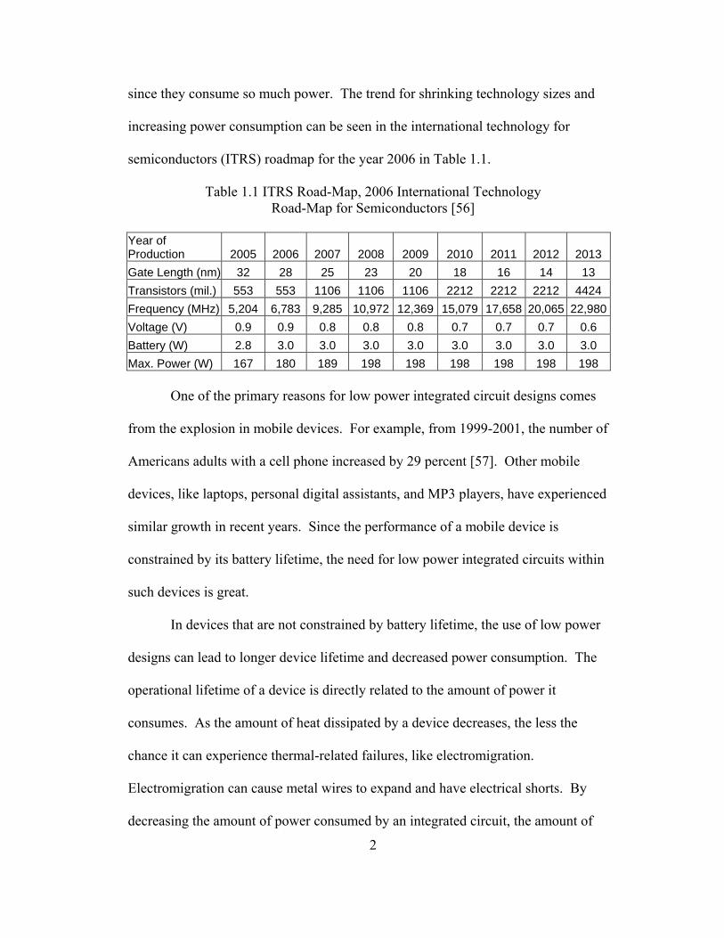
since they consume so much power. The trend for shrinking technology sizes and
increasing power consumption can be seen in the international technology for
semiconductors (ITRS) roadmap for the year 2006 in Table 1.1.
Table 1.1 ITRS Road-Map, 2006 International Technology Road-Map for Semiconductors [56]
Year of Production 2005 2006 2007 2008 2009 2010 2011 2012 2013 Gate Length (nm) 32 28 25 23 20 18 16 14 13 Transistors (mil.) 553 553 1106 1106 1106 2212 2212 2212 4424 Frequency (MHz) 5,204 6,783 9,285 10,972 12,369 15,079 17,658 20,065 22,980Voltage (V) 0.9 0.9 0.8 0.8 0.8 0.7 0.7 0.7 0.6 Battery (W) 2.8 3.0 3.0 3.0 3.0 3.0 3.0 3.0 3.0 Max. Power (W) 167 180 189 198 198 198 198 198 198 One of the primary reasons for low power integrated circuit designs comes
from the explosion in mobile devices. For example, from 1999-2001, the number of
Americans adults with a cell phone increased by 29 percent [57]. Other mobile
devices, like laptops, personal digital assistants, and MP3 players, have experienced
similar growth in recent years. Since the performance of a mobile device is
constrained by its battery lifetime, the need for low power integrated circuits within
such devices is great.
In devices that are not constrained by battery lifetime, the use of low power
designs can lead to longer device lifetime and decreased power consumption. The
operational lifetime of a device is directly related to the amount of power it
consumes. As the amount of heat dissipated by a device decreases, the less the
chance it can experience thermal-related failures, like electromigration.
Electromigration can cause metal wires to expand and have electrical shorts. By
decreasing the amount of power consumed by an integrated circuit, the amount of

3
electricity consumed by the device is lowered. Since global warming is a major
environmental issue and electricity generation leads to environmental and thermal
pollution, by lowering the amount of electricity consumed in a device, the
environment that all humans live in can be sustained.
1.2 Power Consumption
The types of power consumption in an integrated circuit can be divided into
two parts, static power consumption and dynamic power consumption. Static power
consumption is dependent on the layout of transistors within a circuit as well as the
process technology utilized, while dynamic power consumption is dependent on
output transitions that lead to charging and discharging of load capacitances. The
total power consumed by a circuit can be represented by the formula [41]:
Ptotal = Pstatic + Pdynamic (1.1)
1.2.1 Static Power Consumption
The first cause of static power consumption is subthreshold conduction
through OFF transistors. While an ideal OFF transistor has no current flowing
through it, the presence of subthreshold tunneling, leakage, and conduction leads to a
small amount of current moving through the OFF transistor. The second cause of
static power consumption is tunneling current through gate oxide. While silicon
dioxide is a very good insulator, for technology processes that are smaller than
130nm, tunneling current becomes an important factor in static power consumption.
The third cause of static power consumption is leakage through reverse-biased diodes.
As the diffusion regions, wells, and substrate that make up the different parts of a
transistor connect with each other, they create reverse-biased diodes. The static

4
power consumption due to reverse-biased diodes is small compared to subthreshold
conduction or gate tunneling and can generally be ignored. The fourth factor in static
power consumption is contention current in ratioed circuits. For pseudo-nMOS
circuit styles, there is a direct path from power to ground so contention current must
be factored into the total static power consumption. The total static power
consumption of a circuit is the product of the supply voltage and the total leakage
current and is given by the formula [41]:
Pstatic = IstaticVdd (1.2)
1.2.2 Dynamic Power Consumption
The main cause of dynamic power consumption is the charging and
discharging of gate load capacitances. For gates that are driving long interconnect
wires, the parasitic capacitances present on these interconnect lines also contribute to
the total load capacitance. When the output signal of a logic gate goes from low to
high, the total load capacitance of a gate is charged with an energy equivalent to
,CV2dd where C is the total load capacitance and Vdd is the supply voltage. When the
output signal of a logic gate goes from high to low, the energy stored in the total load
capacitance is discharged. The number of times an output signal transitions from zero
to one is known as its switching activity, denoted by α . Given an operating
frequency of f, the dynamic power consumption due to the switching activity of a
circuit is [41]:
fαCVP 2dddynamic = (1.3)
A secondary source of dynamic power consumption comes from short-circuit
currents. Since an input signal cannot rise or fall between a logic one or zero

5
instantaneously, the pMOS and nMOS transistors that are driven by the input signal
will both be ON for a short period of time as the input signal transitions from Vdd to
GND or vice-versa. Since both transistors are ON for a short period of time, this can
lead to a short circuit between Vdd and GND.
1.3 Asynchronous Circuits
Given the rise in transistor densities and power consumption by synchronous
designs, asynchronous circuits are a low-power alternative. Since there is no clock to
synchronize communication in an asynchronous circuit, the only parts of the circuit
that will be contributing to dynamic power consumption are those that are doing a
requested processing action. The following subsections describe how communication
in asynchronous circuits can be accomplished without a global clock as well as
various implementation styles. For an exhaustive overview of asynchronous circuit
design, the reader is directed to [54].
1.3.1 Asynchronous Communication
With the absence of a global clock to synchronize communication between
logic elements, communication must be done another way. The different types of
communication protocols that an asynchronous circuit can use include two-phase and
four-phase handshaking [54].
Mod
ule
A
ModuleB
request
acknowledge
data
Figure 1.1 Asynchronous Communication
An asynchronous communication example is shown in Figure 1.1. There is an
acknowledge signal from Module B to Module A, and there are request and data

6
signals from Module A to Module B. When Module A needs some processing action
performed by Module B, it asserts the request signal. When Module B has finished
performing this processing action, it asserts the acknowledge signal to show that the
data is valid. Upon receipt of the asserted acknowledge signal, Module A lowers the
request signal, and correspondingly, Module B lowers the acknowledge signal. This
type of communication is known as two-phase handshaking and can be seen in Figure
1.2.
ValidData
request
acknowledge
data
ValidData
Figure 1.2 Two-Phase Handshaking
While two-phase handshaking is simple to implement, it is not robust and can
be prone to timing errors. An extension of two-phase handshaking, which is event-
driven, is four-phase handshaking, which is level-driven. During four-phase
handshaking communication, data is valid the entire time the request line is asserted.
The operation of four-phase handshaking can be seen in Figure 1.3.
ValidData
request
acknowledge
data
ValidData
Figure 1.3 Four-Phase Handshaking

7
1.3.2 Asynchronous Circuit Implementation Styles
Asynchronous circuit implementation styles can be categorized based on their
timing model and how they encode data [54]. Huffman circuit styles assume that
both wires and gates have delays. In Huffman circuits, also known as fundamental
mode circuits, all gate and wire delays are limited by an upper bound. In Timed
circuits, both wires and gates are assumed to have a delay. Unlike Huffman circuits,
however, lower bounds in addition to upper bounds are placed on each of the delay
elements in Timed circuits. Muller circuit styles place no bounds on gate delays and
assume that wire delays are negligible. Quasi-delay insensitive (QDI) asynchronous
circuits assume that aside from wires called isochronic forks, no delays are assumed
on wires. Speed-independent and delay-insensitive implementation styles only
assume that delays are present on gates; wires are assumed to have no delays.
In asynchronous circuits, data can also be encoded using one signal line or
two signal lines. Data that is encoded using one signal line is known as single-rail,
while data that is encoded using two signal lines is known as dual-rail. In a dual-rail
encoding, both signal lines must have the same logic value for data to be valid. Since
both signal lines must have the same value for data to be valid, this makes dual-rail
data encodings much more robust against timing errors and hence they are widely
used in speed-independent and delay-insensitive asynchronous circuit design
implementations.
1.4 Motivation
As can clearly be seen from the previous sections, thermal constraints are an
important factor in integrated circuit design. Asynchronous designs are inherently

8
low power, so as synchronous circuit designs dissipate greater power with higher
transistor densities, asynchronous circuits will become more attractive.
However, asynchronous circuits are much more difficult to design than
synchronous circuits. While there are many commercial CAD tools for synchronous
designs, there are very few CAD tools for asynchronous circuit designs. Even though
asynchronous circuits have been used in several large designs, like the AMULET
embedded processor [58] and RAPPID instruction decoder [59], the lack of industrial
tools prevents widespread adoption of the asynchronous design methodology.
Within the integrated circuit design flow, timing, energy, power, and area
constraints need to be checked at every stage. This work addresses the need for a
universal tool or methodology that can accurately estimate the amount of energy
consumed at the gate level in an asynchronous circuit.
1.5 Contributions
This thesis makes several contributions. First, a new methodology for
simulative energy estimation in the asynchronous domain has been developed.
Second, as long as the asynchronous circuits used are based on the handshaking
communication protocol, the proposed methodology can be used for any type of
asynchronous circuit implementation style.
As detailed in the related works, there are no simulative asynchronous energy
estimation methodologies. Simulation of different asynchronous circuits is done
using timed Petri nets. Petri nets can be used to model many things; in this case, they
are used to model gate-level behavior of a circuit. With the introduction of time into
a Petri net, gate and interconnect delays can be modeled; this allows the capture of
9
energy dissipation due to glitches. CPN Tools is used to simulate the timed Petri net
description of a circuit.
This work is the first that integrates energy estimation into gate-level
simulation of asynchronous circuits. This work uses the Balsa high-level
asynchronous synthesis system to produce most of the circuits used. While Balsa can
produce four-phase handshaking, quasi-delay insensitive, and dual-rail delay
insensitive implementations of asynchronous circuits, this work uses four-phase
handshaking circuits due to the extra gate overhead of delay-insensitive circuits and
limitations present in the CPN Tools simulator.
Any other tool besides Balsa that produces structural netlists of asynchronous
circuits could also be integrated into this work. While very small asynchronous
designs of less than 100 gates have been tested, the methodology proposed should be
able to scale into the hundreds and thousands of gates; limitations currently present in
the CPN Tools simulator prevent testing of larger asynchronous circuit designs.
1.6 Related Work
This section describes the work related to this thesis. This includes power
estimation in sequential and combinational circuits and energy estimation in
asynchronous circuits. Power estimation methods exist at the architectural, RTL,
transistor, and gate level. Furthermore, power estimation methods at the gate level
can be subdivided into probabilistic and statistical methods.
10
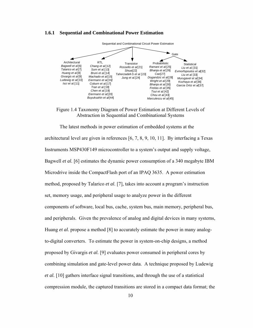
1.6.1 Sequential and Combinational Power Estimation
ArchitecturalBagwell et al. [6]Talarico et al. [7]Huang et al. [8]
Givargis et al. [9]Ludewig et al. [10]
Isci et al. [11]
RTLChang et al. [12]Sum et al. [13]Bruni et al. [14]
Machado et al. [15]Eiermann et al. [16]Coburn et al. [17]Tran et al. [18]Chen et al. [19]
Eiermann et al. [20]Buyuksahin et al. [44]
TransistorRossello et al. [21]
Shiue [22]Taherzadeh- S et al. [23]
Jung et al. [24]
ProbabilisticRamani et al. [25]Bhanja et al. [26]
Cao [27]Dogandzic et al. [28]
Wright et al. [29]Bhanja et al. [30]Freitas et al. [35]Tsui et al. [42]Chou et al. [43]
Marculescu et al. [45]
StatisticalLiu et al. [31]
Evmorfopoulos et al. [32]Liu et al. [33]
Murugavel et al. [34]Kozhaya et al. [36]
Garcia Ortiz et al. [37]
Sequential and Combinational Circuit Power Estimation
Gate
Figure 1.4 Taxonomy Diagram of Power Estimation at Different Levels of Abstraction in Sequential and Combinational Systems
The latest methods in power estimation of embedded systems at the
architectural level are given in references [6, 7, 8, 9, 10, 11]. By interfacing a Texas
Instruments MSP430F149 microcontroller to a system’s output and supply voltage,
Bagwell et al. [6] estimates the dynamic power consumption of a 340 megabyte IBM
Microdrive inside the CompactFlash port of an IPAQ 3635. A power estimation
method, proposed by Talarico et al. [7], takes into account a program’s instruction
set, memory usage, and peripheral usage to analyze power in the different
components of software, local bus, cache, system bus, main memory, peripheral bus,
and peripherals. Given the prevalence of analog and digital devices in many systems,
Huang et al. propose a method [8] to accurately estimate the power in many analog-
to-digital converters. To estimate the power in system-on-chip designs, a method
proposed by Givargis et al. [9] evaluates power consumed in peripheral cores by
combining simulation and gate-level power data. A technique proposed by Ludewig
et al. [10] gathers interface signal transitions, and through the use of a statistical
compression module, the captured transitions are stored in a compact data format; the
11
data is then input into a rapid prototyping system, where the signals can be analyzed,
and the amount of power consumed by the original system can be estimated. To
estimate the power consumed in high-end processors, a technique proposed by Isci et
al. [11] combine real power monitoring and component power estimation; the real
power monitoring hardware consists of a clamp ammeter to measure current, a digital
multimeter to read voltages on the clamp, a logger machine to collect the data, and a
power monitor to display the captured data; the component power estimation part of
this method takes the different components of a processor and their corresponding
access rates to produce a power weight for each component.
The latest methods and applications of RTL power estimation are given in
references [12, 13, 14, 15, 16, 17, 18, 19, 20, 44]. To estimate the power dissipated in
a security processor, Chang et al. [12] use the RTL level description of the processor
to calculate the power dissipated by the processor during AES and RSA encryption
and decryption. A method proposed by Sum et al. [13] uses an up-down encoding
scheme with linear approximation to improve the estimation accuracy of RTL
methods. Bruni et al. [14] propose a RTL power estimation flow that takes into
account propagation delays; while conventional RTL power estimation flows assume
a zero-delay model, the addition of delays allows the calculation of power
consumption due to spurious transitions. Machado et al. [15] propose a technique to
reduce power estimation complexity in VHDL-RTL designs by representing
combinational logic blocks with Binary Decision Diagrams (BDDs). Eiermann et al.
[16] propose several macromodeling techniques for RTL power estimation; the first
modeling technique improves the accuracy of power dissipation caused by word-level
12
switching activity by dividing all input bits into subwords, and the second modeling
technique improves estimation of bit-level switching energy dissipation by adding an
adjustment factor that is related to switching activity at the word-level. Coburn et al.
[17] use specialized power estimation hardware to emulate the power characteristics
of a target system. Tran et al. [18] estimate power consumption by weighting the
total gate-count estimate against five elements of power consumption in a circuit:
logic, on-chip memory, interconnection, clock distribution, and off chip driving I/O.
Chen et al. [19] propose a technique to estimate RTL level power by predicting the
node distribution, capacitance distribution, and entropy distribution of any Boolean
function that is optimized for a minimal area implementation. Eiermann et al. [20]
develop an efficient RTL power modeling technique for combinational logic blocks
by only using word and bit level switching information. Buyuksahin et al. [44]
propose a method for RTL power estimation that takes into account effects of
interconnect loading between gates.
The latest methods for estimating power at the transistor level are given in
references [21, 22, 23, 24]. Rossello et al. [21] propose a model to accurately
estimate the energy dissipated in domino CMOS gates by considering the internal
capacitance switching and discharging currents of such circuits. Shiue [22] proposes
a new analytical model for evaluating power at the transistor level; his analytical
model consists of a α-power law derived from physical MOSFET models, an analysis
of future short-circuit power models, and the equation model from Berkeley BSIM3
manual. Taherzadeh-S et al. [23] develop a new model to calculate the power
consumption of CMOS inverters; the model uses a modified MOSFET short channel

13
n-th power law, and it calculates the short circuit current by using a linear
interpolation scheme. Jung et al. [24] propose a new method for calculating short-
circuit power in static CMOS circuits by accurately deriving short-circuit current
from the interpolation of peak points of actual current curves, which are influenced by
gate-to-drain coupling capacitance.
The latest methods for probabilistic power estimation at the gate level are
given in references [25, 26, 27, 28, 29, 30, 35, 42, 43, 45] Ramani et al. [25] use
Bayesian networks to implement a probabilistic power estimation strategy that is non-
simulative, based on Importance Sampling, and scales efficiently with circuit
complexity. Bhanja et al. [26] use Cascaded Bayesian Networks (CBNs) to estimate
the switching activity of correlated inputs within VLSI circuits; probabilistic
consistency across the CBNs is maintained by a tree-dependent (TD) function, and
the TD function is derived from a minimal weight spanning tree of switching activity
that occurs along pairs of boundary signal lines. Cao [27] uses Bayesian inference
and neural networks to develop a new technique that enables an efficient table-lookup
of power consumption of a circuit’s entire state and transition space. Dogandzic et al.
[28] use sequential Bayesian networks and a Nakagami-m fading model to estimate
the dynamic power of shadow channels in wireless communication networks. Wright
et al. [29] propose a zero-delay probabilistic power estimation technique that uses a
Signal Probability Computation procedure to calculate the signal probability for every
node in a circuit; two representation models presented for a circuit include the
Connective BDD and Integer Pair Representation. Bhanja et al. [30] use logic-
induced directed acyclic graphs (LIDAGs) to model switching probability in a

14
combinational circuit; LIDAGs can be mapped directly to a Bayesian network, which
can be used to model the spatio-temporal correlation of switching activity on a given
node. Freitas et al. [35] solve the Chapman-Kolmogorov equations for sequential
state probabilities by using a discrete Markov chain input to accurately model all
temporal and spatial correlations between internal nodes and primary inputs. A
method by Tsui et al. [42] estimates glitch power by correlating the steady state value
of two signal lines to the probability of them changing state; the greater the transition
probability of an input signal, the greater the glitch power of the circuit. Chou et al.
[43] propose a method to accurately capture switching activity in static and domino
CMOS circuits by considering signal correlations and simultaneous switching among
multiple input signal lines. Marculescu et al. [45] also present a technique to capture
switching activity by considering spatiotemporal correlations under a zero-delay
model.
The latest methods for statistical power estimation at the gate level are given
in references [31, 32, 33, 34, 36, 37]. Liu et al. [31] propose a new binary vector
sequence generator based on a Markov chain (MC) model; the sequence generator
accepts as input an average input probability, an average transition density, and a
spatial correlation factor, and outputs a highly random and uniform vector sequence.
Evmorfopoulos et al. [32] use a Monte Carlo approach based on extreme value theory
to estimate the maximum power dissipation of CMOS VLSI circuits. Liu et al. [33]
propose a new power macromodeling technique that accurately models input glitch
propagation and its affects on energy dissipation within a circuit. Murugavel et al.
[34] propose using sequential and recursive least squares estimation for average
15
power estimation; least squares estimation converges faster than other statistical
methods by attempting to minimize the error of the mean square value during each
successive iteration of the algorithm. Kozhaya et al. [36] use blocks of randomly
selected user-supplied input data to calculate upper and lower bounds on the power
consumption of a circuit. Ortiz et al. [37] extend statistical power estimation methods
to handle the nongaussian data models displayed by portable digital systems.
1.6.2 Asynchronous Energy and Power Estimation
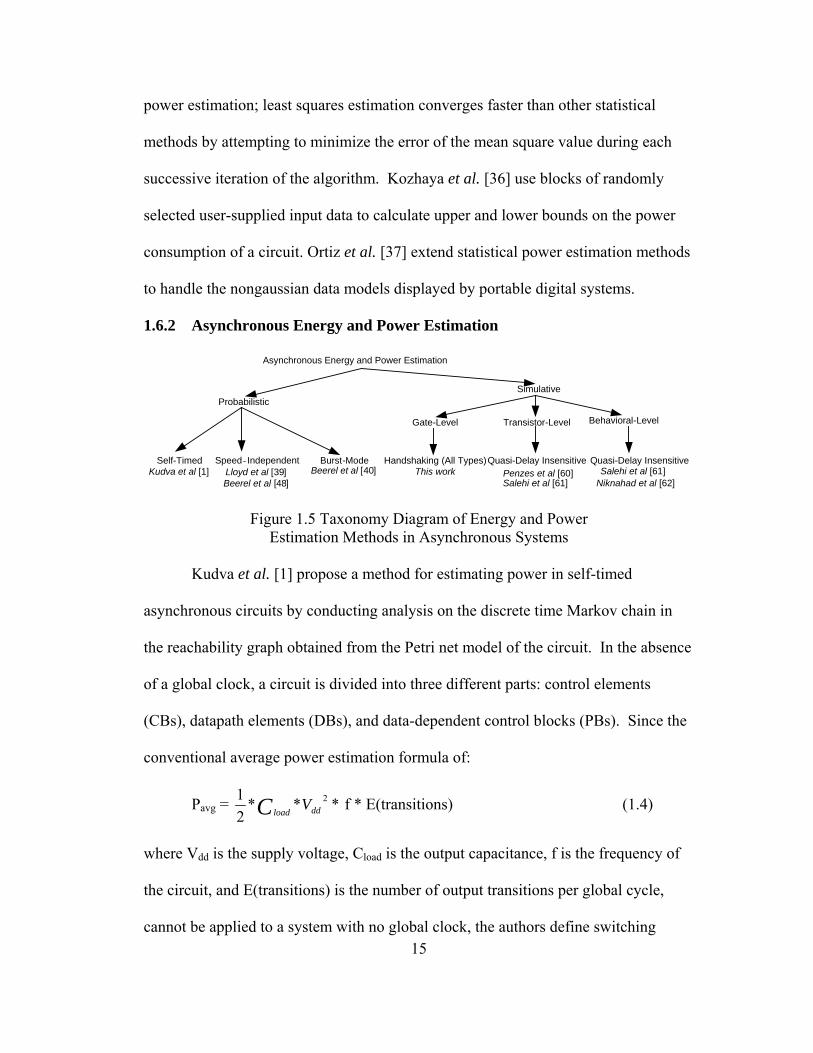
Asynchronous Energy and Power Estimation
Probabilistic
Gate-Level
Lloyd et al [39]Beerel et al 48]
Speed- Independent
[
Burst-ModeBeerel et al [40] This work
Handshaking (All Types)Kudva et al [1]
Self-Timed Quasi-Delay InsensitivePenzes et al [60]Salehi et al [61]
Transistor-Level
Simulative
Behavioral-Level
Quasi-Delay InsensitiveSalehi et al [61]
Niknahad et al [62]
Figure 1.5 Taxonomy Diagram of Energy and Power Estimation Methods in Asynchronous Systems
Kudva et al. [1] propose a method for estimating power in self-timed
asynchronous circuits by conducting analysis on the discrete time Markov chain in
the reachability graph obtained from the Petri net model of the circuit. In the absence
of a global clock, a circuit is divided into three different parts: control elements
(CBs), datapath elements (DBs), and data-dependent control blocks (PBs). Since the
conventional average power estimation formula of:
Pavg = ***21 2
ddloadVC f * E(transitions) (1.4)
where Vdd is the supply voltage, Cload is the output capacitance, f is the frequency of
the circuit, and E(transitions) is the number of output transitions per global cycle,
cannot be applied to a system with no global clock, the authors define switching
16
energy per invocation. An invocation is a request and acknowledge transition pair
between a PB and CB; self-timed circuits communicate using handshaking. The
average switching energy consumed per invocation in a DB is given by:
Einvocation = ***21 2
ddloadVC D(transitions) + Pdt (1.5)
where Vdd is the supply voltage, Cload is the output capacitance, D(transitions) is the
transition density, and Pdt is the energy consumed by the delay line in a PB. The
average switching activity consumed per invocation in a PB is given by:
Einvocation = ***21 2
ddloadVC D(transitions) + Pselect (1.6)
where Pselect is the energy consumed when a request signal is followed by an
acknowledgement signal.
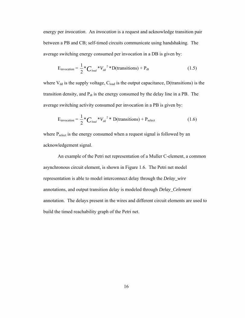
An example of the Petri net representation of a Muller C-element, a common
asynchronous circuit element, is shown in Figure 1.6. The Petri net model
representation is able to model interconnect delay through the Delay_wire
annotations, and output transition delay is modeled through Delay_Celement
annotation. The delays present in the wires and different circuit elements are used to
build the timed reachability graph of the Petri net.

17
Req Ack
Celementout
Delay_wire Delay_wire
Delay_CelementEnergy_Celement
Figure 1.6 Petri Net Representation of Muller C-element [1]
Lloyd et al. [39] propose a method for power estimation in speed-independent
(SI) asynchronous circuits that uses invariant analysis of Petri net models using
matrix representations. An SI circuit assumes all wire delays are negligible compared
to gate output delays; thus, the proposed method is unable to model interconnect
delay and glitch power caused by inputs arriving at different times. While this
method avoids the state space explosion problem by using a matrix representation of
a Petri net, the use of a gate delay model is only suited to SI circuits; the method
described cannot be used to accurately estimate the power consumption in other types
of asynchronous circuits. A method proposed by Beerel et al. [48] derives the
sequential signal transition graph (SSTG) for a circuit. Markov chain analysis is done
on the SSTG such that the average energy consumed per external signal transition is
known.

18
Beerel et al. [40] propose a method for energy estimation in burst-mode
asynchronous circuits. Instead of operating on individual input signals, a burst-mode
circuit operates with bursts of data; for example, an input burst will produce a
corresponding output burst. A burst-mode circuit may have glitches within its
internal signals, but its output is guaranteed to be hazard free. To characterize energy
consumption in absence of a global clock, the average energy per output transition is
considered, whose equation is given by [40]:
***21)( 2
ddloadgategatesVTEn C −
∑= (# of gate switches) (1.7)
Furthermore, upper and lower bounds are placed on the number of gate switches so
that the estimated energy dissipation falls within such bounds.
There are three methods for estimating the energy consumed by quasi-delay
insensitive circuits. Penzes et al. [60] develop a simulator called esim that operates
on a transistor-level description of a QDI asynchronous circuit. They demonstrate
their methodology by estimating the amount of energy consumed by an asynchronous
MIPS R3000 microprocessor. Since many QDI asynchronous circuits are based on
Pre-Charge Full/Half Buffer (PCFB/PCHB) logic, Salehi et al. [61] develop a
methodology to estimate energy consumption by measuring the transition count of
behavioral-level and transistor-level descriptions of QDI circuits using verilog HDL
models. A simulative method developed by Niknahad et al. [62] estimates the power
consumption in QDI circuits at the behavioral-level by counting the number of read
and writes in a circuit.

19
1.7 Thesis Overview
Chapter 2 provides a background on Petri nets and previous related work that
uses Petri nets for power estimation. Chapter 3 provides details of the Petri net
developed to accurately capture the behavior of different gates. Chapter 4 provides
an overview of the power estimation framework used. Chapter 5 provides
experimental results, and Chapter 6 is devoted to conclusions.
20
CHAPTER 2
PETRI NET FRAMEWORK
The first part of this chapter gives a formal introduction to Petri nets and their
operation. The second part of this chapter describes the previous related work that
has been done using Petri nets for power estimation.
2.1 Petri Net Basics
A Petri net model [38] is composed of a set of places and a set of transitions. The
transitions represent an action the model can take, while places represent the state of a
model. To connect the places and transitions in a Petri net, a set of directed arcs are
used. There are two types of directed arcs in a Petri net, input arcs and output arcs.
Input arcs are directed arcs that connect places to transitions. Output arcs are directed
arcs that connect transitions to places. A transition is enabled to fire if all places that
are connected to the input arcs of the transition have a token. Once a transition fires,
tokens from input places are consumed and deposited on places connected by the
output arcs from the transition. The firing of a transition represents a change of state
for the Petri net. The firing of transitions in a Petri net is non-deterministic, which
means if multiple transitions are enabled, then they can fire in any random order. The
initial marking of a Petri net denotes which places of the Petri net are initialized with
tokens. A Petri net can be formally defined:
PN = {P, T, A, P0} (2.1)

21
where:
• P = set of places
• T = set of transitions
• A = set of arcs from places to transitions or transitions to places
• P0 = initial set of marked places
There are many different types of Petri nets: colored, timed, hierarchical,
deterministic, predicate/transition, and stochastic. The basis of this work comes from
colored Petri nets. Colored Petri nets (CP-Nets) are Petri nets that have been
expanded to include color sets, arc expressions, and guard functions. The color sets
in a CP-Net control the type of tokens a place can store as well as determining the
operation and functionality of the overall Petri net. Arc expressions attached to arcs
in a CP-Net can be used to control the binding of token values when a transition fires.
The guard functions in a CP-Net are Boolean expressions attached to transitions. A
guard expression must evaluate to true for a transition in a CP-Net to be enabled to
fire. A CP-Net also has a node function to map arcs to source and destination nodes.
For input arcs in a CP-Net, source nodes are places, and destination nodes are
transitions. For output arcs in a CP-Net, source nodes are transitions, and destination
nodes are places. The initialization function of a CP-Net determines which places
have tokens when the net is initialized. A CP-Net can be formally defined [38]:
CPN = (∑, P, T, A, N, C, G, E, I) (2.2)
where:
• ∑ is a finite set of color sets
• P is a finite set of places
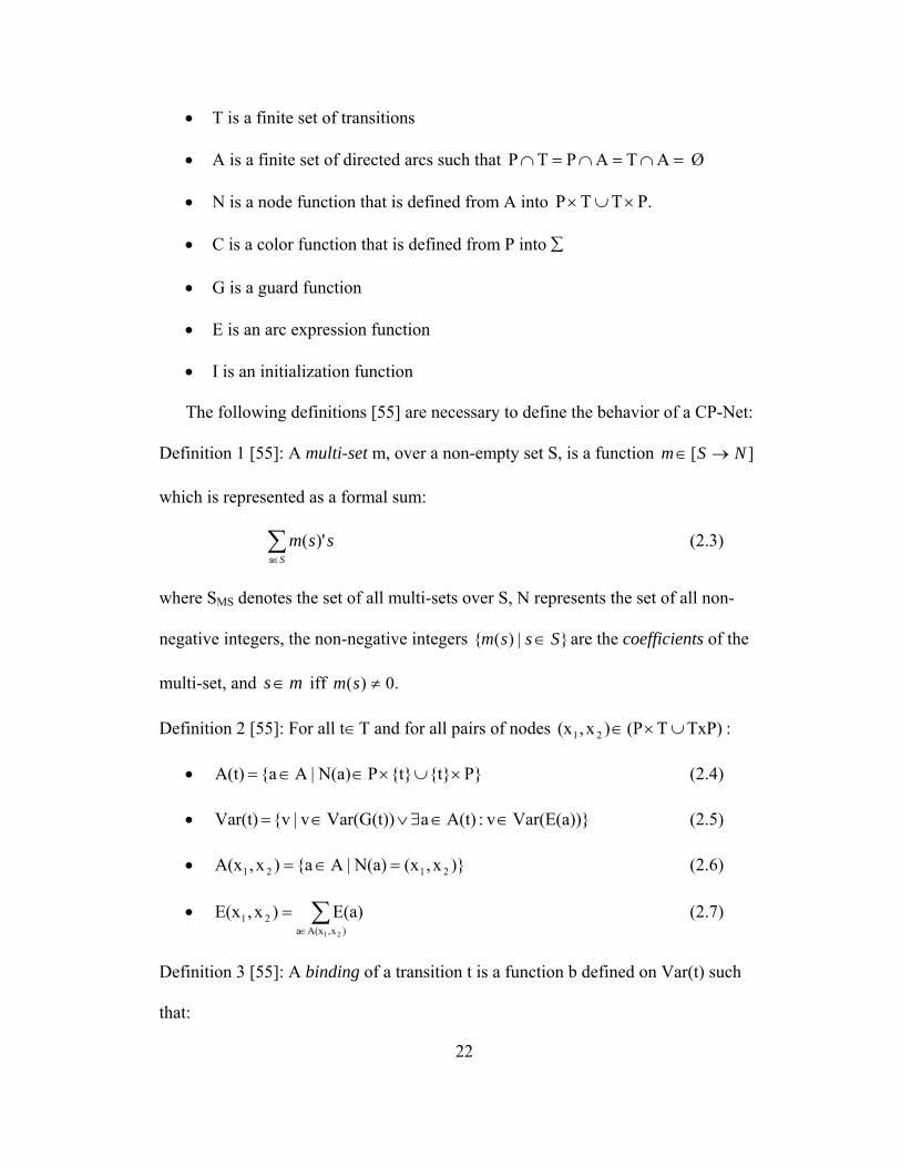
22
• T is a finite set of transitions
• A is a finite set of directed arcs such that =∩=∩=∩ ATAPTP Ø
• N is a node function that is defined from A into P.TTP ×∪×
• C is a color function that is defined from P into ∑
• G is a guard function
• E is an arc expression function
• I is an initialization function
The following definitions [55] are necessary to define the behavior of a CP-Net:
Definition 1 [55]: A multi-set m, over a non-empty set S, is a function ][ NSm →∈
which is represented as a formal sum:
∑∈Ss
ssm )'( (2.3)
where SMS denotes the set of all multi-sets over S, N represents the set of all non-
negative integers, the non-negative integers }|)({ Sssm ∈ are the coefficients of the
multi-set, and ms ∈ iff .0)( ≠sm
Definition 2 [55]: For all t∈T and for all pairs of nodes TxP)T(P)x,(x 21 ∪×∈ :
• P}{t}{t}PN(a)|A{aA(t) ×∪×∈∈= (2.4)
• Var(E(a))}v:A(t)a Var(G(t))v|{v Var(t) ∈∈∃∨∈= (2.5)
• )}x,(xN(a)|A{a)x,A(x 2121 =∈= (2.6)
• ∑∈
=)x,A(xa
2121
E(a))x,E(x (2.7)
Definition 3 [55]: A binding of a transition t is a function b defined on Var(t) such
that:

23
• Type(v)b(v):Var(t)v ∈∈∀ (2.8)
• G(t)<b> (2.9)
where B(t) is the set of all bindings for t, G(t)<b> denotes the evaluation of the guard
expression G(t) in the binding b, and Type(v) denotes the type of a variable v
Definition 4 [55]: A token element is a pair (p, c) where p∈P and c∈C(p), while a
binding element is a pair (t, b) where t∈T and b∈B(t). The set of all token elements
is denoted by TE while the set of all binding elements is denoted by BE.
A marking is a multi-set over TE while a step is a non-empty and finite multi-set over
BE. The initial marking M0 is the marking which is obtained by evaluating the
initialization expression:
I(p))(c)(c) p,(M :TEc) (p, 0 =∈∀ (2.10)
The initialization expression that determines the initial marking M0 for all places p
and all colors c is given by (I(p))(c). The sets of all markings and steps are denoted by
M and Y, respectively.
Definition 5 [55]: A step Y is enabled in a marking M iff the following property is
satisfied:
∑∈
≤⟩⟨∈∀Yb)(t,
M(p) bt)E(p,:Pp (2.11)
where ⟩⟨bt)E(p, denotes an expression evaluation that removes tokens from place p
and fires transition t with the binding b. Once property 2.7 is satisfied, (t,b) and t are
said to be enabled. When a step Y is enabled in a marking M1 it may occur, changing
the marking M1 to another marking M2 defined by:
24
∑∑∈∈
⟩⟨+⟩⟨=∈∀Yb)(t,Yb)(t,
12 bt)E(p,)bt)E(p,-(p)M(p)(M:Pp (2.12)
M2 is directly reachable from M1. This is written [ 21 MYM ⟩ .
Definition 6 [55]: A finite occurrence sequence is a sequence of markings and steps:
[ [ [ 1nnn32211 MYM . . . MYMYM +⟩⟩⟩ (2.13)
such that n∈N, and [ 1iii MYM +⟩ for all i∈{1, 2, …, n} M1 is the start marking, Mn+1
is the end marking and n is the length. Analogously, an infinite occurrence sequence
is a sequence of markings and steps:
[ [ . . . MYMYM 32211 ⟩⟩ (2.14)
such that [ 1iii MYM +⟩ for all 1.i ≥ A marking M" is reachable from a marking M'
iff there exists a finite occurrence sequence starting in M' and ending in M" . The set
of markings that is reachable from M' is denoted by [ ⟩M' . A marking is reachable iff
it belongs to [ ⟩'M0 .
CP-Nets can also be augmented to include hierarchy and time. Hierarchical
CP-Nets (HCPNs) are the foundation for a new class of Petri net that can be used to
model an asynchronous circuit. To accurately describe the behavior of HCPNs, the
following definitions are needed:
Definition 7 [38]: A time set (TS) is defined as the set of all non-negative real
numbers, TS = x∈R, where x represents the time instant and R is the set of all real
numbers.
Definition 8 [38]: For each transition t∈T, Var(t) is the set of variables associated
with transition t given as,

25
Var(E(a))}v:A(t)aVar(G(t))v|{vVar(t):Tt ∈∈∃∨∈=∈∀ (2.15)
where, v is the variables in the Petri net, Var(G(t)) is the set of variables associated
with the Guard-expression (G), a is the arcs in the Petri net, A(t) is the set of arcs
associated with transition t, and E(a) is the arc-expression associated with arc a.
2.2 Power Estimation Using Petri Nets
Since this work uses Petri nets to model asynchronous systems at the gate
level, it draws heavily on the work done previously in [3, 4] for power estimation in
combinational and sequential circuits. This section describes the work done in [3, 4,
5]. Murugavel et al. [3] develop the foundation for power estimation in
combinational circuits through the use of Hierarchical Colored Hardware Petri nets
(HCHPNs). A basic HCHPN is a structural model of a gate. HCHPNs are derived
from colored Petri nets (CPNs). A HCHPN [3] is defined as the set
HCHPN = (PG, ST, GT, TI, TO, TC, RP) (2.16)
where:
• PG is a finite set of non-hierarchical CPN
• TST ⊆ where ST is a set of substitution transitions (super nodes)
• ( TGT ⊆ and STGT ∩ = Ø), where GT is the set of gate transitions
• TI is the time set defined as the set of all nonnegative real numbers, TI = x∈R,
where x represents the time instant and R the set of all real numbers
• TO is the set of all possible colored tokens
• TC is the code segment function. It is defined from T into the set of functions
• PRP ⊂ is a set of restricted places, which can hold only a finite numbers of
tokens in them.
26
PI 1
PI 2
P0
P1
P2
P3
P4
P5
PO
w
w
w
w
w
w
w
ww
w
w
w ww
w
w
: place
: transition
: restricted place
: gate transition
W : ( # of tokens, type of token = 0 or 1)
w0: ( # of tokens, type of token = 0 only)
w1: ( # of tokens, type of token = 0 only)
T0
T1
T2
T3
T4
T5
T6
T7
w0w0
w0
w0
w0
w0w0
w0
w1
w1
w1
w1w1
w1
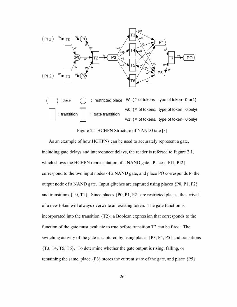
Figure 2.1 HCHPN Structure of NAND Gate [3]
As an example of how HCHPNs can be used to accurately represent a gate,
including gate delays and interconnect delays, the reader is referred to Figure 2.1,
which shows the HCHPN representation of a NAND gate. Places {PI1, PI2}
correspond to the two input nodes of a NAND gate, and place PO corresponds to the
output node of a NAND gate. Input glitches are captured using places {P0, P1, P2}
and transitions {T0, T1}. Since places {P0, P1, P2} are restricted places, the arrival
of a new token will always overwrite an existing token. The gate function is
incorporated into the transition {T2}; a Boolean expression that corresponds to the
function of the gate must evaluate to true before transition T2 can be fired. The
switching activity of the gate is captured by using places {P3, P4, P5} and transitions
{T3, T4, T5, T6}. To determine whether the gate output is rising, falling, or
remaining the same, place {P3} stores the current state of the gate, and place {P5}

27
stores the previous state of the gate. Transitions {T3, T4, T5, T6} correspond to
different types of switching activity within a gate:
• T3 fires if the output of the gate remains at logic ‘0’
• T4 fires if the output falls from logic ‘1’ to logic ‘0’ (power dissipation)
• T5 fires if the output rises from logic ‘0’ to logic ‘1’ (power consumption)
• T6 fires if the output of the gate remains at logic ‘1’
The output of the transitions {T3, T4, T5, T6} is stored in places {P4, P5}. The
temporal correlation between different tokens is modeled using transition {T7} and
places {P4, P5}. The structural HCHPN model of the NAND gate serves as the basis
for future Petri net development work; it is able to accurately model the delay, gate
function, switching activity, glitch power, and overall power consumption present
within the gate.
Murugavel et al. [4] extend the HCHPN described previously to handle sequential
circuits. Since sequential circuits are basically combinational circuits with delayed
output feedback and flipflops, it is not hard to modify a combinational HCHPN to
account for the unique temporal and spatial relationships present within a sequential
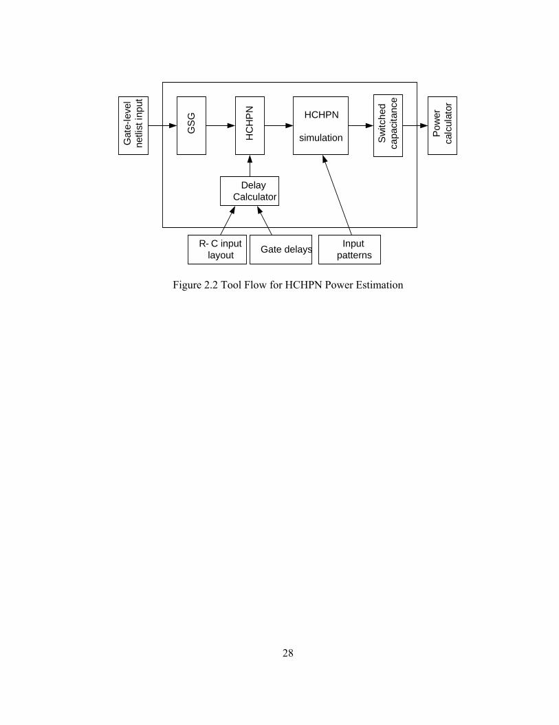
circuit. The tool flow for power estimation using HCHPNs is shown in Figure 2.2.
Since the HCHPN [3] serves as the foundation for future Petri net modeling of
asynchronous systems, it is logical that the tool flow for switching activity and energy
estimation would be similar to the ones used in references [3, 5].
28
Gat
e-le
vel
netli
st in
put
GS
G
HC
HP
N HCHPN
simulation Switc
hed
capa
cita
nce
Pow
erca
lcul
ator
DelayCalculator
R- C inputlayout Gate delays Input
patterns
Figure 2.2 Tool Flow for HCHPN Power Estimation

29
CHAPTER 3
PETRI NET MODELING OF ASYNCHRONOUS CIRCUITS FOR ENERGY ESTIMATION
In this chapter, a new type of Petri net for energy estimation in asynchronous
circuits is presented. The first part of this chapter gives the formal definition for the
new type of Petri net. The second part of this chapter describes how basic logic gates
can be modeled using the new type of Petri net. Within each subsection of the second
part of this chapter, detailed firing examples are given to show how the Petri net
operates. The third and final part of this chapter describes how an asynchronous
circuit can be transformed into the new type of Petri net while preserving its behavior
and timing information.
3.1 Hierarchical Colored Asynchronous Hardware Petri Nets
To develop a new type of Petri net that can accurately model the gate delays
and interconnect delays present in a circuit, the factor of time must be added. Also,
since communication in asynchronous circuits is predominantly based on
request/acknowledge handshaking, the number of invocations in a circuit must also be
modeled. To accomplish these goals, a new type of Petri net, called Hierarchical
Colored Asynchronous Hardware Petri net (HCAHPN), has been developed. The
features of HCAHPNs are:

30
• Gate delays and interconnect delays of a circuit are accurately captured
• Special substitution transitions count the number of request and acknowledge
signal pairs to determine the number of invocations in a circuit
• When gate transitions fire in a HCAHPN, it is the equivalent of a gate
evaluating to a logic one or zero
• Each token in a HCAHPN has a time stamp. The token is only available to be
consumed by transitions if its time value is equal to or less than the current
simulator time.
To accurately model each gate in a high-level circuit, a HCAHPN has a set of
substitution transitions. Each substitution transition in a HCAHPN corresponds to a
subnet that accurately models a primitive gate. A signal propagating through a logic
gate in a circuit is analogous to a token propagating through a substitution transition
in a HCAHPN. In addition to substitution transitions, the HCAHPN also has a set of
gate transitions that take into account the value of input tokens and produce an
appropriate output token. The logic behavior of a gate is accurately modeled by gate
transitions within a HCAHPN. Depending on what type of signal a gate is driving, a
substitution transition can be classified as a request or acknowledge substitution
transition. In these special types of substitution transitions, the switching activity
recorded within the subnet also serves to record the number of request and
acknowledge signal changes. A token in a HCAHPN is defined by the tuple (p, v, n,
t), where p is the place of the token, v is the color of the token, n is the port number of
the token, and t is the time stamp value of the token. The color value of the token is
used to represent the logic value of a signal. The port number of a token is used to

31
determine from which input signal to a gate the token came from; it can also be used
to denote a gate output signal or control the enabling of transitions. Code segments
can also be attached to arcs and transitions to control the flow and values of tokens.
A HCAHPN can be defined mathematically as follows.
Definition 9: A HCAHPN can be defined as a tuple:
HCAHPN = (CP, ST, GT, TS, CT, CS, RST, AST) (3.1)
where:
• CP is a set of non-hierarchical CP-Nets
• ST is a set of substitution transitions such that TST ⊆
• GT is a set of gate transitions such that TGT ⊆ and STGT ∩ = Ø
• TS is the time set as defined previously in definition 7 of section 2.1
• CT is the set of all possible colored tokens denoted by the tuple (p, v, n, t),
where p∈P, v is the value of the token, n is the port number of the token, and
t∈TS
• CS is the code segment function. It maps code segments into the set of gate
transitions GT, the set of guard functions G, and the set of arc expressions E.
• RST is the set of request substitution transitions such that STRST ⊆ and
ASTRST ∩ = Ø
• AST is the set of acknowledge substitution transitions such that
STAST ⊆ and ASTRST ∩ = Ø
The following definitions are necessary to define the various features of a
HCAHPN, which is useful for modeling asynchronous circuits:
Definition 10: For each CP-Net cp ∈ CP, the following characteristics hold:

32
• =∩ cp(a))-(CP(a) cp(a) Ø (3.2)
• =∩ cp(p))-(CP(p) cp(p) Ø (3.3)
• =∩ cp(t))-(CP(t) cp(t) Ø (3.4)
where cp(a) denotes the set of arcs associated with cp, CP(a) denotes the set of all
arcs in CP, cp(p) denotes the set of places associated with cp, CP(p) denotes the set of
all places in CP, cp(t) denotes the set of transitions associated with cp, and CP(t)
denotes the set of all transitions in CP.
Definition 11: A token element in a HCAHPN is a tuple (p, v, n, t) where p ∈ P,
v∈C(p), n∈C(p), and t∈TS.
Definition 12: A Firing (t, x, y) specifies the possibility of the firing of transition t by
removing tokens from the input places x attached to transition t and depositing tokens
to the output places y attached to transition t. The set of all firings is the Firing set
FS.
Definition 13: The enabling time F of a firing (t, x, y) is the maximal value of the
time-stamps of all the tokens in the set of input places x when transition t fires.
xCT t)n, v,(p,max b)a,F(t,
∈= (3.5)
Definition 14: If a transition t is enabled and the global clock is greater than or equal
to the enabling time, it can fire. If more than one transition is enabled to fire at the
same time, one transition is non-deterministically selected from the set of enabled
transitions to fire. The global clock does not increment until all enabled transitions at
the given time have fired.
33
3.2 HCAHPN Low-Level Modeling
A
BZ
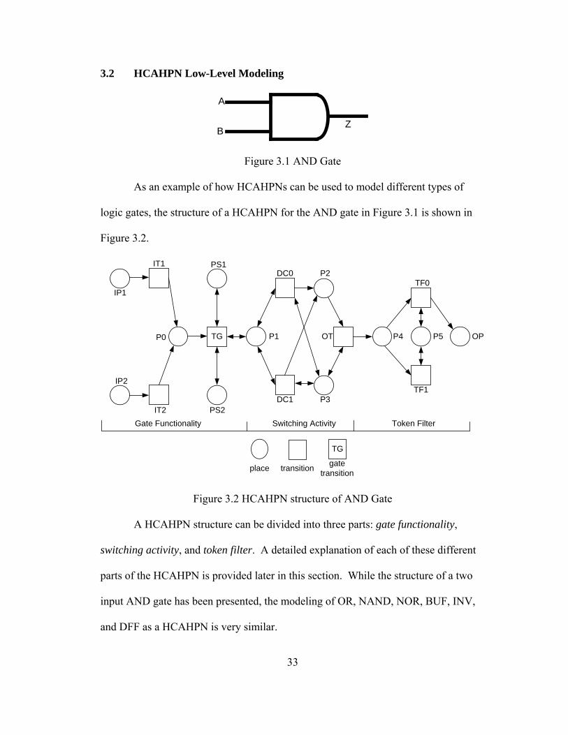
Figure 3.1 AND Gate
As an example of how HCAHPNs can be used to model different types of
logic gates, the structure of a HCAHPN for the AND gate in Figure 3.1 is shown in
Figure 3.2.
TG
IP1
IP2
IT2
IT1
P0
PS1
PS2
P1
DC0
DC1
P2
P3
OT P4 P5
TF0
TF1
OP
place transition
TG
gate transition
Gate Functionality Switching Activity Token Filter
Figure 3.2 HCAHPN structure of AND Gate
A HCAHPN structure can be divided into three parts: gate functionality,
switching activity, and token filter. A detailed explanation of each of these different
parts of the HCAHPN is provided later in this section. While the structure of a two
input AND gate has been presented, the modeling of OR, NAND, NOR, BUF, INV,
and DFF as a HCAHPN is very similar.

34
3.2.1 Gate Functionality Substructure
IP1
IP2
P0
IT2
IT1(v, p)
(v, p)
TG
PS1
PS2
P1
input (v, p, v1, v2)output (vO, pO);actionletin if p = 1 andalso (v = 1 andalso v2 = 1) then (1, 0) else if p = 2 andalso (v =1 andalso v1 = 1) then (1, 0) else (0, 0)end;
(v, 1)
(v, 2)
(v, p)
if p = p1then (v, 1)
else (v1, 1)
if p = p2then (v, 2)
else (v2, 2)
(v1, p1)
(v2, p2)
(vO, pO) @+ 159
(v3, p3) @+ 158
Gate Transition Code Segment
place transition
TG
gate transition
v, v1, v2, v3, vO: Token Logic Variables
p, p1, p2, p3, pO: Token Port Number Variables
@+
arc delay
Figure 3.3 Gate Functionality Structure Detail of AND Gate
The details of the gate functionality Petri net substructure of a HCAHPN
model for an AND gate are shown in Figure 3.3. The variables present on the
different arcs are used to bind token values. It is important to note that the scope of
each variable is local to each transition. For example, the scope of the variable set (v,
p) attached to transition {IT2} is different from the variable set (v, p) attached to
transition {TG}. Once all variables attached to a transition can be bound to a value
from their respective tokens, that transition is enabled to fire.
The places {IP1, IP2} are used to model the two input ports of an AND gate.
The transitions {IT1, IT2} are used to propagate tokens from places {IP1, IP2} to
place {P0}. The places {PS1, PS2} are used to store the current value of inputs A
and B respectively. Place {P0} is used to store the value of current inputs to the

35
circuit. By the structure of the Petri net, the capacity of places {PS1, PS2} is limited
to one token. Through the use of a code segment function, transition {TG} is able to
use the value of tokens from places {P0, PS1, PS2} to model the functionality of the
gate. The delay on the arc from transition {TG} to place {P1} is used to model the
intrinsic gate delay of the AND gate.
While place {P0} can store multiple tokens, a token is only available once its
time stamp is equal to the simulator time. If there are multiple input tokens on place
{P0} with successively increasing time stamp values, the simulator will evaluate each
token deterministically as simulator time increases and each token becomes available
to the simulator. If two tokens have a time stamp value of i at place {P0}, then at
time i the transition {TG} will non-deterministically choose one token to consume.
At time i + 1, the transition {TG} will fire again to consume the second token at
place {P0}. Since intrinsic gate delay is much greater than 1 time unit and the token
at place {P1} is not available until the gate output finishes transitioning, this very
small non-deterministic behavior is acceptable.
Since there must be tokens present for a transition to fire, the initialization
function is used to initialize tokens at places {PS1, PS2, P1}. Since the tuple
(v, p, n, t) is the set of values a token can take, the following is a formal description of
how the initialization function initializes tokens at places {PS1, PS2, P1}
• PS1 = (0, 1, PS1, 0)
• PS2 = (0, 2, PS2, 0)
• P1 = (0, 100, P1, 0)

36
The port number value of a token serves two purposes. First, it is used to
represent from which input port a token came from. For example, as a token
propagates from place {IP1} to place {P0} through transition {IT1}, its port value is
forced to 1. Second, its value is used as part of a guard function on transitions. A
port number value of 0 designates that the token is an output. Place P1 is initialized
with a token whose port number value is 100. Since there are no gates with one
hundred input ports, this arbitrary value was chosen to control the firing of transitions
in the switching activity substructure of the HCAHPN.
Within CPN Tools, delays can be specified on transitions, input arcs, and output
arcs. While an HCHPN uses transition delays to model intrinsic gate delays, a
HCAHPN uses delays on output arcs to model intrinsic gate delays. A delay on an
arc or transition updates the time value of all output tokens attached to the arc or
transition. A token is only available to be used by a transition if its time value is less
than or equal to the current simulator time. If gate delays were specified on transition
{TG}, then the firing of the Petri net could become non-deterministic. For example,
suppose transition {TG} has just fired and the time value of tokens at places {P0,
PS1, PS2, P1} is 159 time units greater than the current simulator time. The tokens at
these places are not available to be used by any transitions until the current simulator
time has incremented an additional 159 time units. During the incrementing of
simulator time, places {IP1, IP2} each receive a token. Once 159 time units have
passed, the tokens at places {P0, PS1, PS2, P1} are available to be used by
transitions. This situation leads to a non-deterministic firing of the transitions {IT1,
37
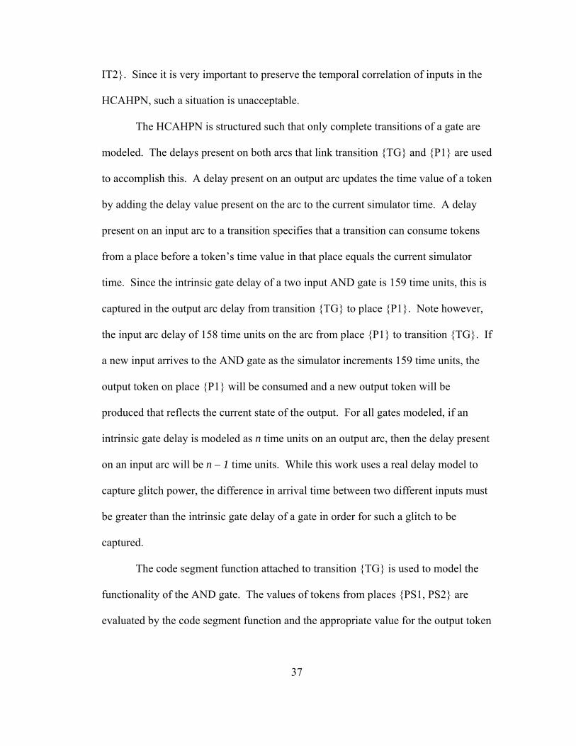
IT2}. Since it is very important to preserve the temporal correlation of inputs in the
HCAHPN, such a situation is unacceptable.
The HCAHPN is structured such that only complete transitions of a gate are
modeled. The delays present on both arcs that link transition {TG} and {P1} are used
to accomplish this. A delay present on an output arc updates the time value of a token
by adding the delay value present on the arc to the current simulator time. A delay
present on an input arc to a transition specifies that a transition can consume tokens
from a place before a token’s time value in that place equals the current simulator
time. Since the intrinsic gate delay of a two input AND gate is 159 time units, this is
captured in the output arc delay from transition {TG} to place {P1}. Note however,
the input arc delay of 158 time units on the arc from place {P1} to transition {TG}. If
a new input arrives to the AND gate as the simulator increments 159 time units, the
output token on place {P1} will be consumed and a new output token will be
produced that reflects the current state of the output. For all gates modeled, if an
intrinsic gate delay is modeled as n time units on an output arc, then the delay present
on an input arc will be n – 1 time units. While this work uses a real delay model to
capture glitch power, the difference in arrival time between two different inputs must
be greater than the intrinsic gate delay of a gate in order for such a glitch to be
captured.
The code segment function attached to transition {TG} is used to model the
functionality of the AND gate. The values of tokens from places {PS1, PS2} are
evaluated by the code segment function and the appropriate value for the output token
38
is chosen. The coding language used to describe the code segment function is
Standard ML.
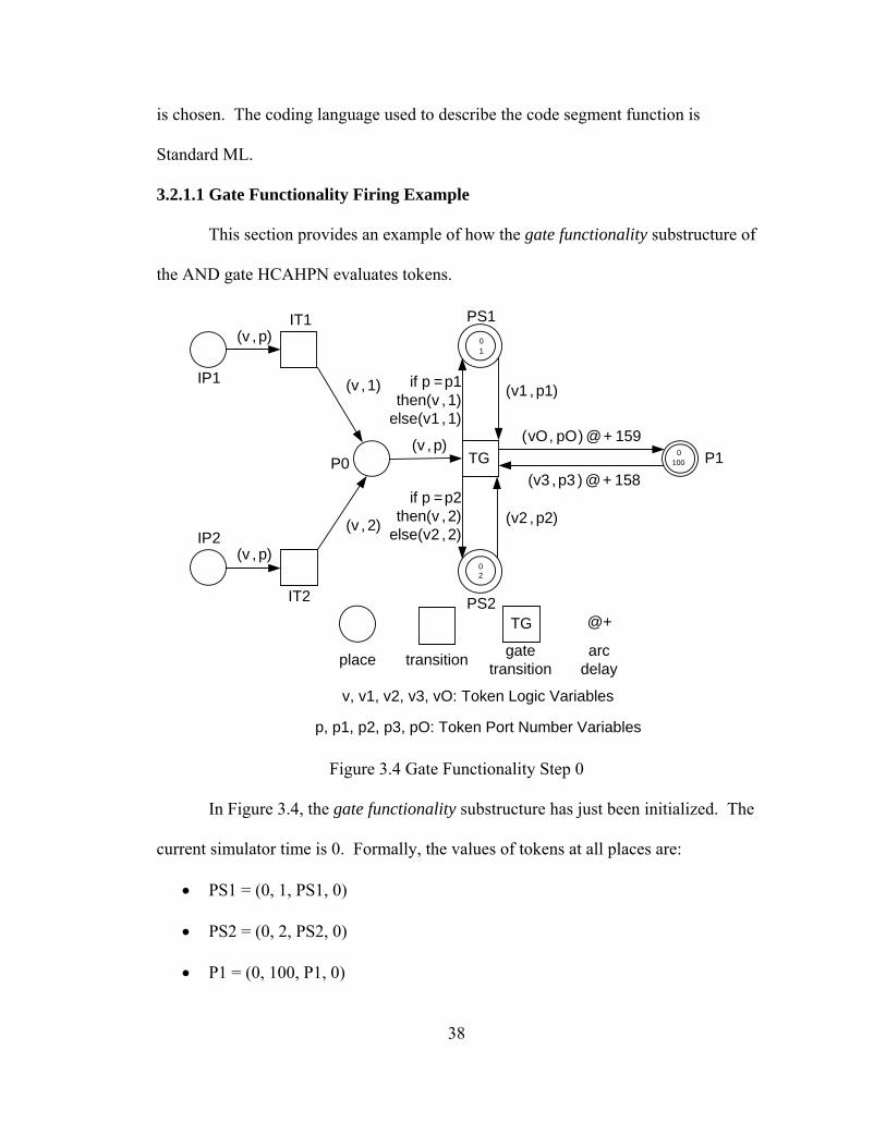
3.2.1.1 Gate Functionality Firing Example
This section provides an example of how the gate functionality substructure of
the AND gate HCAHPN evaluates tokens.
(v , p)
(v , p)
TG
(v , 1)
(v , 2)
(v , p)
if p = p1then (v , 1)
else (v1 , 1)
if p = p2then (v , 2)
else (v2 , 2)
(v1 , p1)
(v2 , p2)
(vO, pO) @+ 159
(v3 , p3 ) @+ 158
0100
02
01
place transition
TG
gate transition
v, v1, v2, v3, vO: Token Logic Variables
p, p1, p2, p3, pO: Token Port Number Variables
@+
arc delay
IT2
IT1
IP1
IP2
P0 P1
PS2
PS1
Figure 3.4 Gate Functionality Step 0
In Figure 3.4, the gate functionality substructure has just been initialized. The
current simulator time is 0. Formally, the values of tokens at all places are:
• PS1 = (0, 1, PS1, 0)
• PS2 = (0, 2, PS2, 0)
• P1 = (0, 100, P1, 0)

39
(v, p)
(v, p)
TG
(v, 1)
(v, 2)
(v, p)
if p = p1then (v, 1)
else (v1, 1)
if p = p2then (v, 2)
else (v2, 2)
(v1, p1)
(v2, p2)
(vO, pO) @+ 159
(v3, p3) @+ 158
0100
02
01
10
IP2
place transition
TG
gate transition
v, v1, v2, v3, vO: Token Logic Variables
p, p1, p2, p3, pO: Token Port Number Variables
@+
arc delay
IP1
P0 P1
IT2
IT1
PS2
PS1
Figure 3.5 Gate Functionality Step 1
At simulator time 160, a new input token arrives at place IP1, as shown in
Figure 3.5. With the arrival of token at place {IP1}, transition {IT1} is enabled to
fire. On the inbound arc to the transition, variable v is bound to 1, and variable p is
bound to 0. On the outbound arc from the transition, the logic value of the token
remains the same, but the port value is changed from 0 to 1. The simulator time is
still 160. Formally, the value of tokens at all places are:
• PS1 = (0, 1, PS1, 0)
• PS2 = (0, 2, PS2, 0)
• P1 = (0, 100, P1, 0)
• IP1 = (1, 0, IP1, 160)
40
(v, p)
(v, p)
TG
(v, 1)
(v, 2)
(v, p)
if p = p1then (v, 1)
else (v1, 1)
if p = p2then (v, 2)
else (v2, 2)
(v1, p1)
(v2, p2)
(vO, pO) @+ 159
(v3, p3) @+ 158
0100
02
01
11
place transition
TG
gate transition
v, v1, v2, v3, vO: Token Logic Variables
p, p1, p2, p3, pO: Token Port Number Variables
@+
arc delay
IP2
IP1
IT2
IT1 PS1
PS2
P0 P1
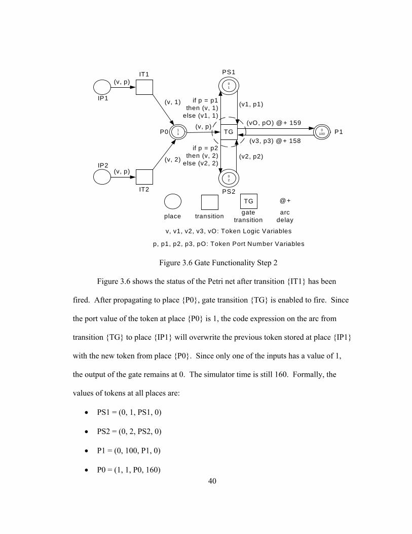
Figure 3.6 Gate Functionality Step 2
Figure 3.6 shows the status of the Petri net after transition {IT1} has been
fired. After propagating to place {P0}, gate transition {TG} is enabled to fire. Since
the port value of the token at place {P0} is 1, the code expression on the arc from
transition {TG} to place {IP1} will overwrite the previous token stored at place {IP1}
with the new token from place {P0}. Since only one of the inputs has a value of 1,
the output of the gate remains at 0. The simulator time is still 160. Formally, the
values of tokens at all places are:
• PS1 = (0, 1, PS1, 0)
• PS2 = (0, 2, PS2, 0)
• P1 = (0, 100, P1, 0)
• P0 = (1, 1, P0, 160)

41
(v, p)
(v, p)
TG
(v, 1)
(v, 2)
(v, p)
if p = p1then (v, 1)
else (v1, 1)
if p = p2then (v, 2)
else (v2, 2)
(v1, p1)
(v2, p2)
(vO, pO) @+ 159
(v3, p3) @+ 158
00
02
11
place transition
TG
gate transition
v, v1, v2, v3, vO: Token Logic Variables
p, p1, p2, p3, pO: Token Port Number Variables
@+
arc delay
IP2
IP1
IT1
IT2 PS2
PS1
P0 P1
Figure 3.7 Gate Functionality Step 3
The status of the Petri net after gate transition {TG} fires is shown in Figure 3.7.
Note that the time stamp of token at place {P1} has been incremented by 159 time
units. It will be available to the simulator at time 319. The input arc from place {P1}
to transition {TG}, however, allows transition {TG} to access the token at place {P1}
up to 158 time units before the simulator time equals 319. The simulator time is still
160. Formally, the values of tokens at all places are:
• PS1 = (1, 1, PS1, 160)
• PS2 = (0, 2, PS2, 160)
• P1 = (0, 0, P1, 319)

42
(v, p)
(v, p)
TG
(v, 1)
(v, 2)
(v, p)
if p = p1then (v, 1)
else (v1, 1)
if p = p2then (v, 2)
else (v2, 2)
(v1, p1)
(v2, p2)
(vO, pO) @+ 159
(v3, p3) @+ 158
00
02
11
10
place transition
TG
gate transition
v, v1, v2, v3, vO: Token Logic Variables
p, p1, p2, p3, pO: Token Port Number Variables
@+
arc delay
IT2
IT1
IP2
IP1
PS2
PS1
P1P0
Figure 3.8 Gate Functionality Step 4
When simulator time reaches 300 however, a new input token arrives at input
place {IP2} as shown in Figure 3.8. Transition {IT2} is enabled to fire. On the
inbound arc to the transition, variable v is bound to 1, and variable p is bound to 0.
On the outbound arc from the transition, the logic value of the token remains the
same, but the port value is changed from 0 to 2. The simulator time is 300. Formally,
the values of tokens at all places are:
• PS1 = (1, 1, PS1, 160)
• PS2 = (0, 2, PS2, 160)
• P1 = (0, 0, P1, 319)
• IP2 = (1, 0, IP2, 300)

43
(v , p )
(v , p )
T G
(v , 1 )
(v , 2 )
(v , p )
if p = p1the n (v , 1 )
e lse (v1 , 1 )
if p = p2the n (v , 2 )
e lse (v2 , 2 )
(v1 , p 1 )
(v2 , p 2 )
(vO , pO ) @ + 1 59
(v3 , p3 ) @ + 158
00
02
11
12
p la ce trans itio n
T G
ga te tra ns ition
v , v1 , v2 , v3 , vO : T oken L og ic V a ria b le s
p , p1 , p2 , p 3 , p O : T oken P o rt N u m ber V a riab les
@ +
a rc de la y
P S 2
P S 1
P 1P 0
IT 2
IT 1
IP 2
IP 1
Figure 3.9 Gate Functionality Step 5
After transition {IT2} fires, the gate transition {TG} is enabled to fire, as
shown in Figure 3.9. Since the port value of the token at place {P0} is 2, the code
expression on the arc from transition {TG} to place {IP2} will overwrite the previous
token stored at place {IP2} with the new token from place {P0}. Since both of the
inputs have a value of 1, the output of the gate will transition to 1. The simulator time
is still 300. The delay expression on the input arc from place {P1} to transition {TG}
allows transition {TG} to consume the token at place {P1}. Formally, the values of
tokens at all places are:
• PS1 = (1, 1, PS1, 160)
• PS2 = (0, 2, PS2, 160)
• P1 = (0, 0, P1, 319)
• P0 = (1, 2, P0, 300)
44
(v, p)
(v, p)
TG
(v, 1)
(v, 2)
(v, p)
if p = p1then (v, 1)
else (v1, 1)
if p = p2then (v, 2)
else (v2, 2)
(v1, p1)
(v2, p2)
(vO, pO) @+ 159
(v3, p3) @+ 158
11
12
10
place transition
TG
gate transition
v, v1, v2, v3, vO: Token Logic Variables
p, p1, p2, p3, pO: Token Port Number Variables
@+
arc delay
PS2
PS1
P1P0
IT1
IT2
IP2
IP1
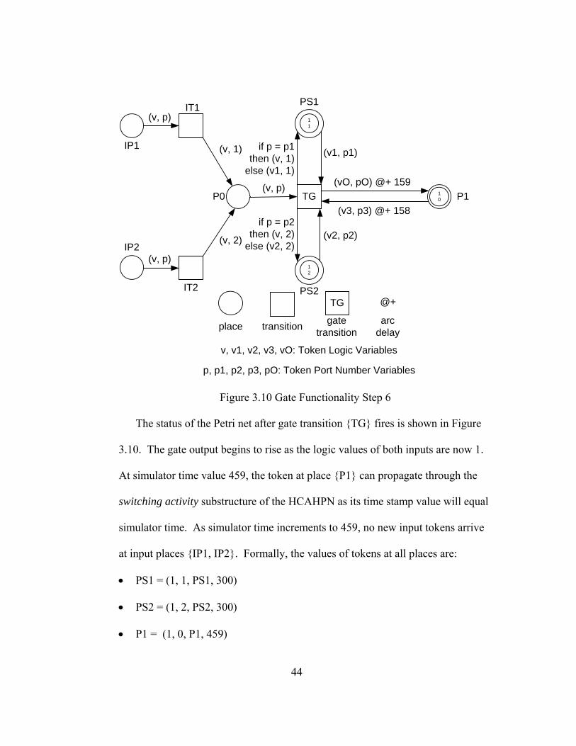
Figure 3.10 Gate Functionality Step 6
The status of the Petri net after gate transition {TG} fires is shown in Figure
3.10. The gate output begins to rise as the logic values of both inputs are now 1.
At simulator time value 459, the token at place {P1} can propagate through the
switching activity substructure of the HCAHPN as its time stamp value will equal
simulator time. As simulator time increments to 459, no new input tokens arrive
at input places {IP1, IP2}. Formally, the values of tokens at all places are:
• PS1 = (1, 1, PS1, 300)
• PS2 = (1, 2, PS2, 300)
• P1 = (1, 0, P1, 459)

45
3.2.2 Switching Activity Substructure
(v1, p1)
(v1, p1)
(v, p)
(v, p)
(v, p)
(v, p)
(v, 100)
(v, 100)
(v, p)
(v, p)
(v1, p1)
(v, p)
place transition
v, v1: Token Logic Variables
p, p1: Token Port Number Variables
DC0
DC1 P3
OT
P2
P4P1
Figure 3.11 Switching Activity Structure Detail of AND Gate
The details of the switching activity Petri net substructure of a HCAHPN
model for an AND gate are shown in Figure 3.11. The current output of the gate is
stored at place P1. Once the time value of the token at place P1 is equal to the current
simulator time, it is available to transitions {DC0, DC1}. Note the arcs from
transitions {DC0, DC1} to place {P1} that set the port value of a token to 100. Part
of the guard functions present on the transitions {DC0, DC1} specifies that the
transitions are only enabled if the port value of a token present at place {P1} is not
equal to 100. Also, a token must be present on place {P4} for transition {TG} to be
enabled.

46
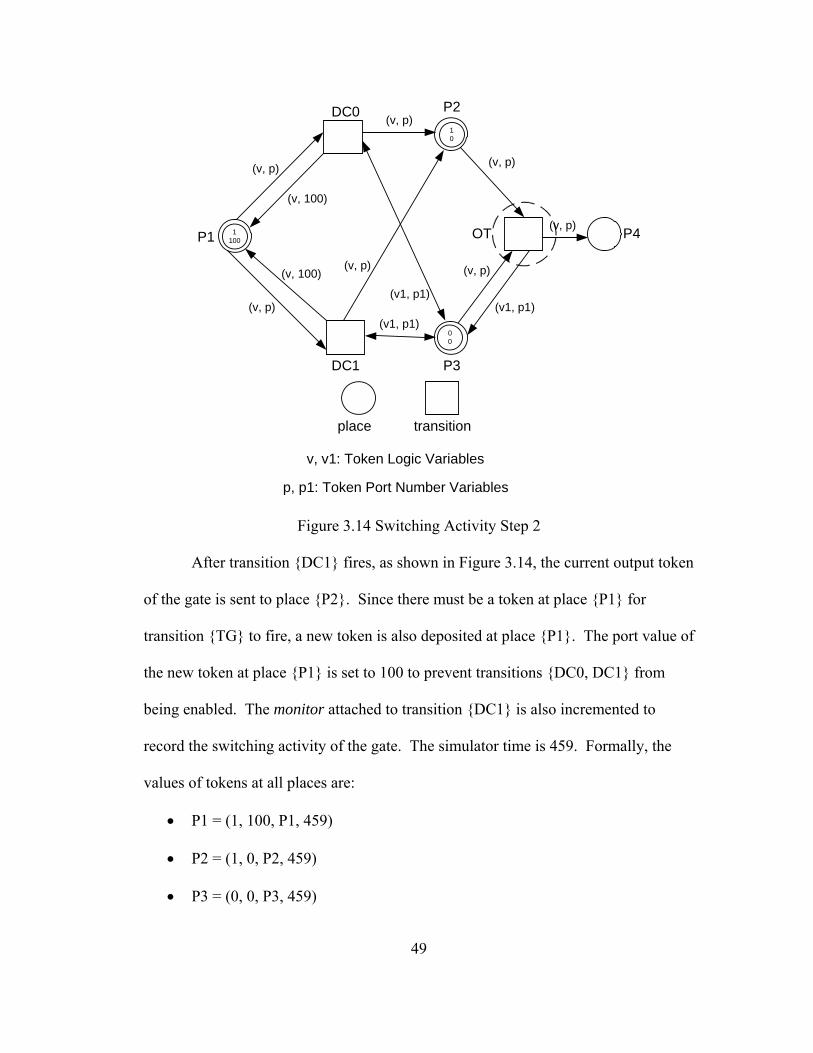
The switching activity substructure of a HCAHPN is similar to that of an
HCHPN. Place {P3} is used to hold the previous output of the gate. Once an
appropriate transition from the set {DC0, DC1} has fired, the current state of the gate
will be reflected at the token on place {P2}. After transition {OT} fires, the token
value present at place {P2} is propagated to places {P3, P4}. The previous state of
the gate that is reflected by the value of token at place {P3} before the firing of
transition {OT} is overwritten by the value of the token from place {P2} after
transition {OT} fires. Each transition from the set {DC0, DC1} is enabled depending
on the current state and previous state of the output of the gate.
• Transition DC0 fires if the gate output remains the same
• Transition DC1 fires if the gate output is rising or falling
Within CPN Tools, monitors are attached to transition DC1 to record the
switching activity of the output of the gate. For gates that are driving request or
acknowledge signals, the monitor attached to transition DC1 also serves to record the
number of request and acknowledge signal assertions.
There is no token present at place P2 when the Petri net is initialized. The
initialization function initializes tokens at places {P1, P3} to the following values:
• P1 = (0, 100, P1, 0)
• P3 = (0, 0, P3, 0)
47
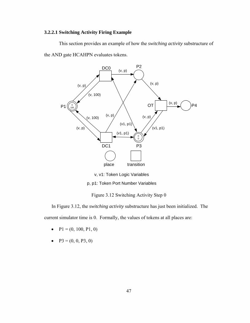
3.2.2.1 Switching Activity Firing Example
This section provides an example of how the switching activity substructure of
the AND gate HCAHPN evaluates tokens.
(v1, p1)
(v1, p1)
(v, p)
(v, p)
(v, p)
(v, p)
(v, 100)
(v, 100)
(v, p)
(v, p)
(v1, p1)
(v, p)
place transition
v, v1: Token Logic Variables
p, p1: Token Port Number Variables
DC0
DC1 P3
OT
P2
P4P1 0100
00
Figure 3.12 Switching Activity Step 0
In Figure 3.12, the switching activity substructure has just been initialized. The
current simulator time is 0. Formally, the values of tokens at all places are:
• P1 = (0, 100, P1, 0)
• P3 = (0, 0, P3, 0)

48
(v1, p1)
(v1, p1)
(v, p)
(v, p)
(v, p)
(v, p)
(v, 100)
(v, 100)
(v, p)
(v, p)
(v1, p1)
(v, p)
place transition
v, v1: Token Logic Variables
p, p1: Token Port Number Variables
DC0
DC1 P3
OT
P2
P4P1 10
00
Figure 3.13 Switching Activity Step 1
At simulator time 459, a new token is available to the simulator at place {P1},
as shown in Figure 3.13. Since the new token’s output value is different from the
previous output token value stored at place {P3}, transition {DC1} is enabled to fire.
The simulator time is 459. Formally, the values of tokens at all places are:
• P1 = (1, 0, P1, 459)
• P3 = (0, 0, P3, 0)
49
(v1, p1)
(v1, p1)
(v, p)
(v, p)
(v, p)
(v, p)
(v, 100)
(v, 100)
(v, p)
(v, p)
(v1, p1)
(v, p)
place transition
v, v1: Token Logic Variables
p, p1: Token Port Number Variables
DC0
DC1 P3
OT
P2
P4P1 1100
00
10
Figure 3.14 Switching Activity Step 2
After transition {DC1} fires, as shown in Figure 3.14, the current output token
of the gate is sent to place {P2}. Since there must be a token at place {P1} for
transition {TG} to fire, a new token is also deposited at place {P1}. The port value of
the new token at place {P1} is set to 100 to prevent transitions {DC0, DC1} from
being enabled. The monitor attached to transition {DC1} is also incremented to
record the switching activity of the gate. The simulator time is 459. Formally, the
values of tokens at all places are:
• P1 = (1, 100, P1, 459)
• P2 = (1, 0, P2, 459)
• P3 = (0, 0, P3, 459)

50
(v1, p1)
(v1, p1)
(v, p)
(v, p)
(v, p)
(v, p)
(v, 100)
(v, 100)
(v, p)
(v, p)
(v1, p1)
(v, p)
10
1100
10
place transition
v, v1: Token Logic Variables
p, p1: Token Port Number Variables
P3DC1
P1
DC0 P2
OT
Figure 3.15 Switching Activity Step 3
After transition {OT} fires, as shown in Figure 3.15, the current output token
of the gate overwrites the previous output token of the gate which was stored at place
{P3}. The simulator time is 459. The output token at place {P4} is free to propagate
to the Token Filter substructure of the HCAHPN. Formally, the values of tokens at all
places are:
• P1 = (1, 100, P1, 459)
• P3 = (1, 0, P3, 459)
• P4 = (1, 0, P4, 459)

51
3.2.3 Token Filter Substructure
P4 P5
TF0
TF1
(v , p)
(v , p)
(v , p)
(v , p) (v1 , p1)
(v1 , p1)
OP
(v , p)
[ v != v 1 | p 1 = 100]
[ v = v 1 & p 1 != 100]
place transition
v, v1: Token Logic Variables
p, p1: Token Port Number Variables
Figure 3.16 Token Filter Structure Detail of AND Gate
The details of the Token Filter Petri net substructure of a HCAHPN model for
an AND gate are shown in Figure 3.16. This substructure is designed to limit
simulation overhead by only propagating output tokens that are different from the
previous output value. The exception to this rule is the very first output token. When
a circuit first becomes operational, the state of a signal between two gates is
unknown. Once the signal state between two gates is established, only changes in
those signal states need to be propagated.
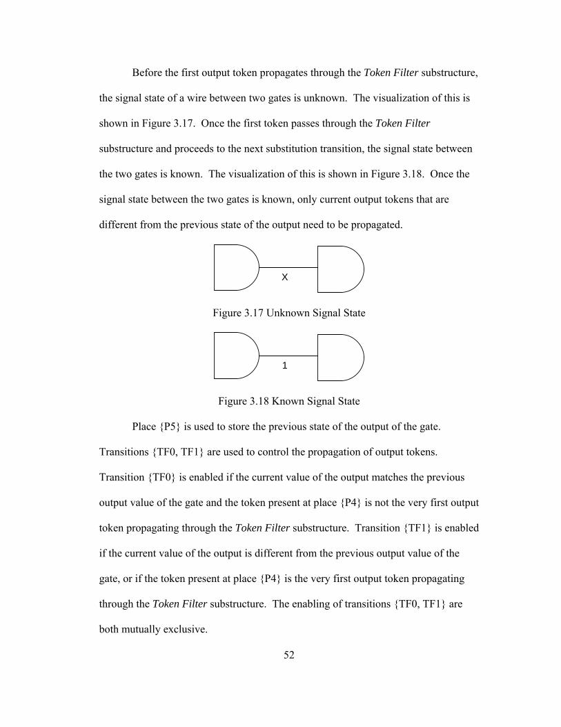
52
Before the first output token propagates through the Token Filter substructure,
the signal state of a wire between two gates is unknown. The visualization of this is
shown in Figure 3.17. Once the first token passes through the Token Filter
substructure and proceeds to the next substitution transition, the signal state between
the two gates is known. The visualization of this is shown in Figure 3.18. Once the
signal state between the two gates is known, only current output tokens that are
different from the previous state of the output need to be propagated.
X
Figure 3.17 Unknown Signal State
1
Figure 3.18 Known Signal State
Place {P5} is used to store the previous state of the output of the gate.
Transitions {TF0, TF1} are used to control the propagation of output tokens.
Transition {TF0} is enabled if the current value of the output matches the previous
output value of the gate and the token present at place {P4} is not the very first output
token propagating through the Token Filter substructure. Transition {TF1} is enabled
if the current value of the output is different from the previous output value of the
gate, or if the token present at place {P4} is the very first output token propagating
through the Token Filter substructure. The enabling of transitions {TF0, TF1} are
both mutually exclusive.
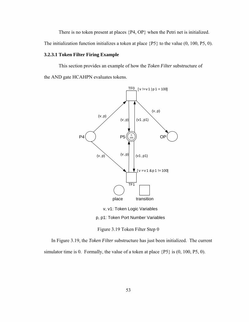
53
There is no token present at places {P4, OP} when the Petri net is initialized.
The initialization function initializes a token at place {P5} to the value (0, 100, P5, 0).
3.2.3.1 Token Filter Firing Example
This section provides an example of how the Token Filter substructure of
the AND gate HCAHPN evaluates tokens.
P4 P5
TF0
TF1
(v , p)
(v , p)
(v , p)
(v , p) (v1 , p1)
(v1 , p1)
OP
(v , p)
[ v != v 1 | p 1 = 100]
[ v = v 1 & p 1 != 100]
place transition
v, v1: Token Logic Variables
p, p1: Token Port Number Variables
0100
Figure 3.19 Token Filter Step 0
In Figure 3.19, the Token Filter substructure has just been initialized. The current
simulator time is 0. Formally, the value of a token at place {P5} is (0, 100, P5, 0).
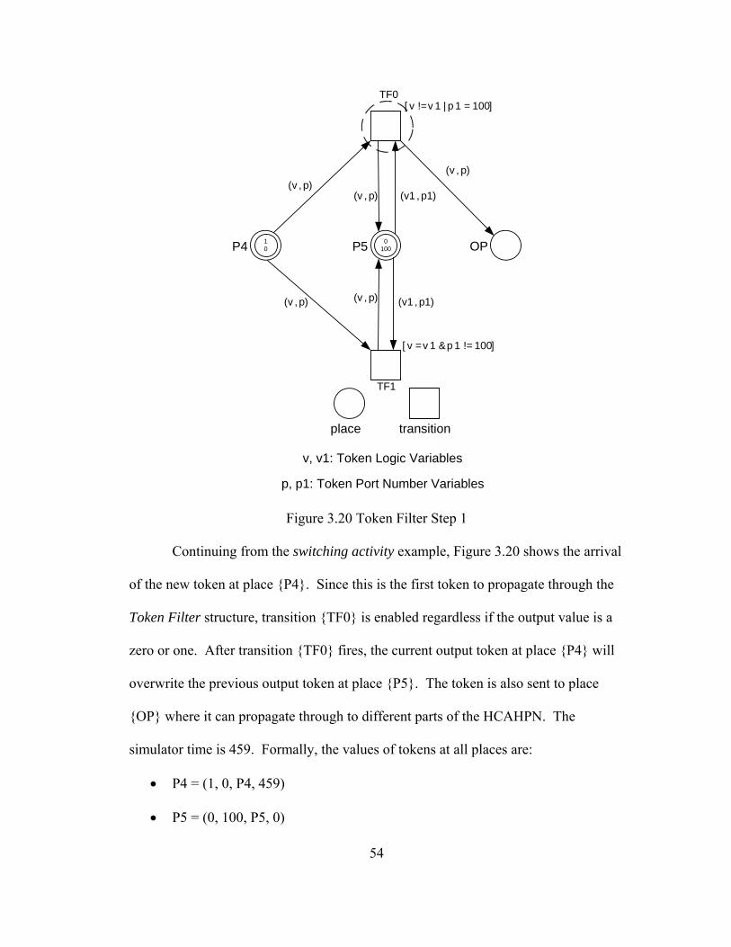
54
P4 P5
TF0
TF1
(v , p)
(v , p)
(v , p)
(v , p) (v1 , p1)
(v1 , p1)
OP
(v , p)
[ v != v 1 | p 1 = 100]
[ v = v 1 & p 1 != 100]
place transition
v, v1: Token Logic Variables
p, p1: Token Port Number Variables
0100
10
Figure 3.20 Token Filter Step 1
Continuing from the switching activity example, Figure 3.20 shows the arrival
of the new token at place {P4}. Since this is the first token to propagate through the
Token Filter structure, transition {TF0} is enabled regardless if the output value is a
zero or one. After transition {TF0} fires, the current output token at place {P4} will
overwrite the previous output token at place {P5}. The token is also sent to place
{OP} where it can propagate through to different parts of the HCAHPN. The
simulator time is 459. Formally, the values of tokens at all places are:
• P4 = (1, 0, P4, 459)
• P5 = (0, 100, P5, 0)
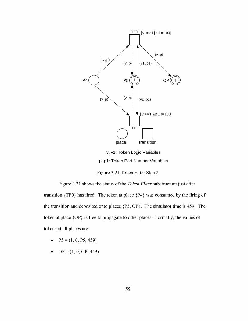
55
P4 P5
TF0
TF1
(v , p)
(v , p)
(v , p)
(v , p) (v1 , p1)
(v1 , p1)
OP
(v , p)
[ v != v 1 | p 1 = 100]
[ v = v 1 & p 1 != 100]
place transition
v, v1: Token Logic Variables
p, p1: Token Port Number Variables
10
10
Figure 3.21 Token Filter Step 2
Figure 3.21 shows the status of the Token Filter substructure just after
transition {TF0} has fired. The token at place {P4} was consumed by the firing of
the transition and deposited onto places {P5, OP}. The simulator time is 459. The
token at place {OP} is free to propagate to other places. Formally, the values of
tokens at all places are:
• P5 = (1, 0, P5, 459)
• OP = (1, 0, OP, 459)

56
3.3 HCAHPN High-Level Modeling
The goal of turning an asynchronous circuit into a HCAHPN is to accurately
capture switching activity and the number of request and acknowledge signal
assertions. During this conversion process, the circuit behavior and timing
information must be preserved. As an example of this process, the wine shop [54]
asynchronous circuit is shown in Figure 3.22.
C
C req_ patron
ack_ patron
req_wine
ack_wine
inv1_out
inv2_out
C1
C2
Figure 3.22 Wine Shop Asynchronous Circuit
The wine shop asynchronous circuit consists of two inverters and two Muller
C-elements. Muller C-elements are commonly used logic gates in asynchronous
circuits and are usually not available in most synchronous standard cell libraries.
Since this work integrates a synchronous standard cell library, Muller C-elements are
realized by feeding a 3-input OR gate with three 2-input AND gates. The next step is
to flatten the wine shop down to its primitive gate cells. The flattened wine shop can
be seen in Figure 3.23.
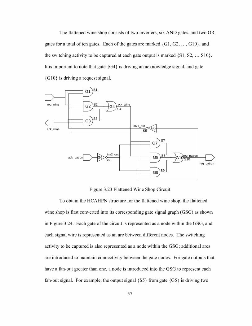
57
The flattened wine shop consists of two inverters, six AND gates, and two OR
gates for a total of ten gates. Each of the gates are marked {G1, G2, …, G10}, and
the switching activity to be captured at each gate output is marked {S1, S2, … S10}.
It is important to note that gate {G4} is driving an acknowledge signal, and gate
{G10} is driving a request signal.
_
_
inv1_out
inv2_out
G1
G2
G3
G4
G5
G7
G8
G9
G10G6
S1
S2
S3
S4
S5
S6
S7
S8
S9
S10ack_patron
ack_wine
req_wine ack_wine
req_patron
req_patron
Figure 3.23 Flattened Wine Shop Circuit
To obtain the HCAHPN structure for the flattened wine shop, the flattened
wine shop is first converted into its corresponding gate signal graph (GSG) as shown
in Figure 3.24. Each gate of the circuit is represented as a node within the GSG, and
each signal wire is represented as an arc between different nodes. The switching
activity to be captured is also represented as a node within the GSG; additional arcs
are introduced to maintain connectivity between the gate nodes. For gate outputs that
have a fan-out greater than one, a node is introduced into the GSG to represent each
fan-out signal. For example, the output signal {S5} from gate {G5} is driving two
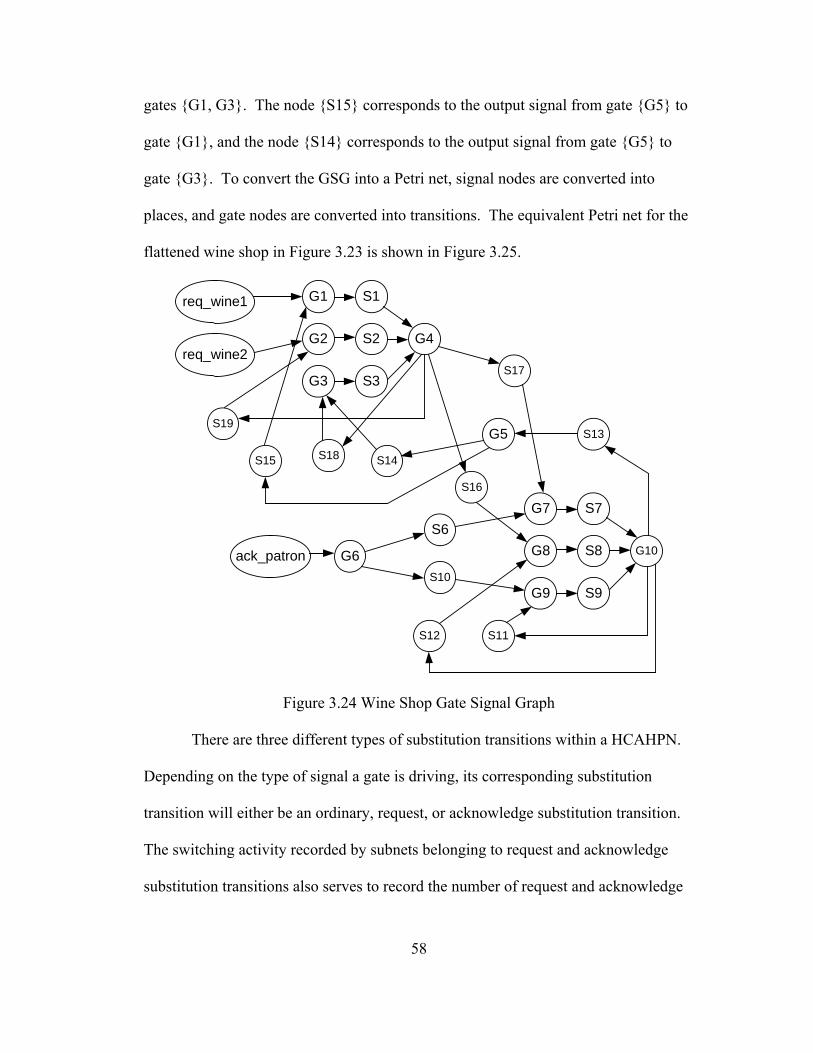
58
gates {G1, G3}. The node {S15} corresponds to the output signal from gate {G5} to
gate {G1}, and the node {S14} corresponds to the output signal from gate {G5} to
gate {G3}. To convert the GSG into a Petri net, signal nodes are converted into
places, and gate nodes are converted into transitions. The equivalent Petri net for the
flattened wine shop in Figure 3.23 is shown in Figure 3.25.
req_wine1 G1
G2
G3
S1
S2
S3
G7
G8
G9
S7
S8
S9
G4
G10G6
S6
S10
S12 S11
G5 S13
S14S15
S17
S16
S18
S19
req_wine2
ack_patron
Figure 3.24 Wine Shop Gate Signal Graph
There are three different types of substitution transitions within a HCAHPN.
Depending on the type of signal a gate is driving, its corresponding substitution
transition will either be an ordinary, request, or acknowledge substitution transition.
The switching activity recorded by subnets belonging to request and acknowledge
substitution transitions also serves to record the number of request and acknowledge
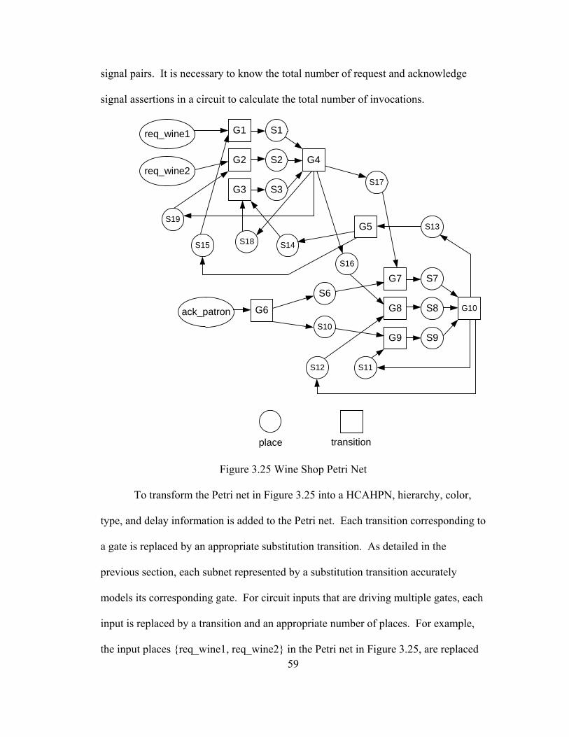
59
signal pairs. It is necessary to know the total number of request and acknowledge
signal assertions in a circuit to calculate the total number of invocations.
req_wine1 S1
S2
S3
S7
S8
S9
S6
S10
S12 S11
S13
S14S15
S17
S16
S18
S19
req_wine2
ack_patron
G1
G2
G3
G4
G6
G5
G7
G8
G9
G10
place transition
Figure 3.25 Wine Shop Petri Net
To transform the Petri net in Figure 3.25 into a HCAHPN, hierarchy, color,
type, and delay information is added to the Petri net. Each transition corresponding to
a gate is replaced by an appropriate substitution transition. As detailed in the
previous section, each subnet represented by a substitution transition accurately
models its corresponding gate. For circuit inputs that are driving multiple gates, each
input is replaced by a transition and an appropriate number of places. For example,
the input places {req_wine1, req_wine2} in the Petri net in Figure 3.25, are replaced

60
by a single transition that is connected to two places. For gates that are driving
request and acknowledge signal wires, they are replaced by their appropriate request
and acknowledge substitution transitions. For example, since gate {G10} is driving a
request signal, it is replaced by a corresponding request substitution transition.
Interconnect delay is represented by adding delay information to arcs. The HCAHPN
structure for the flattened wine shop is shown in Figure 3.26.
req_wine
S1
S2
S3
S7
S8
S9
S6
S10
S12 S11
S13
S14S15
S17
S16
S18
S19
ack_patron
place transition substitutiontransition
requestsubstitutiontransition
acknowledgesubstitutiontransition
G10
G9
G8
G7
G1
G2
G3G3
G6
G5
G4T1
R1
R2
d
d
d
d
d
d
d
dd
d
d
d
d
d
d
d
d
d
d
d
delay
Figure 3.26 Wine Shop HCAHPN
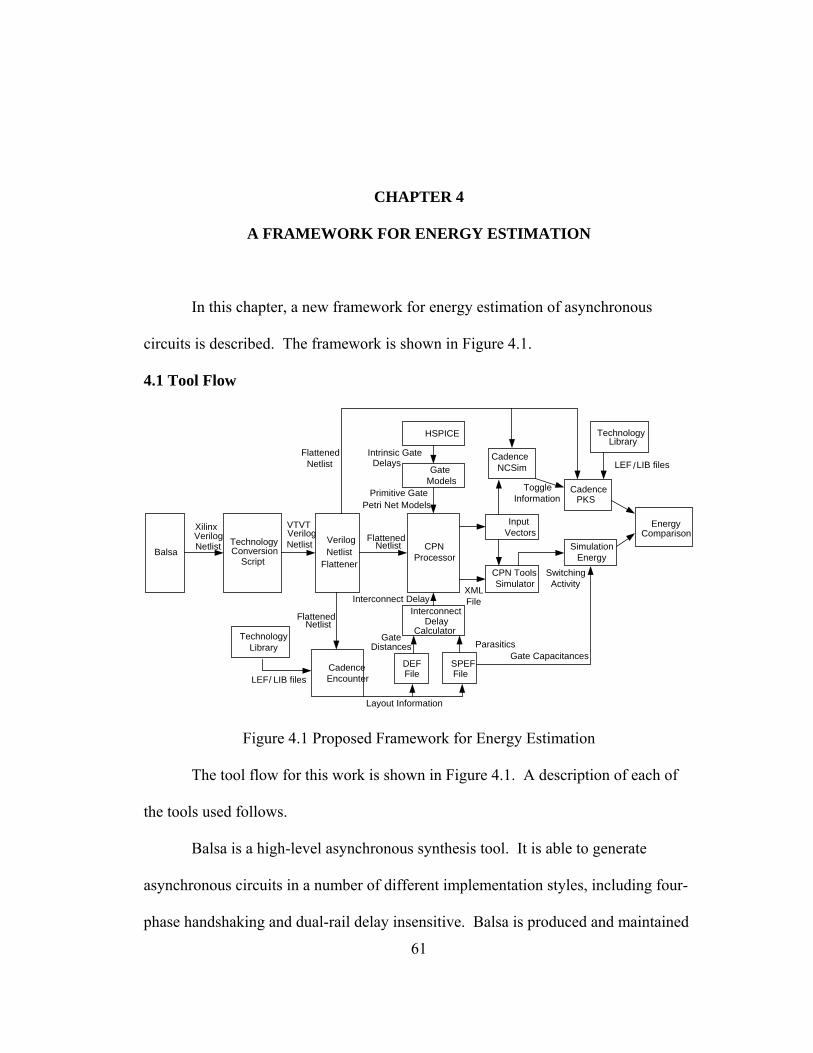
61
CHAPTER 4
A FRAMEWORK FOR ENERGY ESTIMATION
In this chapter, a new framework for energy estimation of asynchronous
circuits is described. The framework is shown in Figure 4.1.
4.1 Tool Flow
BalsaVerilogNetlist
Flattener
TechnologyConversion
ScriptCPN
Processor
XilinxVerilogNetlist
VTVTVerilogNetlist
FlattenedNetlist
CadenceEncounter
FlattenedNetlist
DEFFile
SPEFFile
InterconnectDelay
Calculator
Layout Information
ParasiticsGate
Distances
Interconnect Delay
HSPICE
GateModels
Intrinsic Gate Delays
Primitive Gate Petri Net Models
CPN ToolsSimulator
InputVectors
SimulationEnergy
CadencePKS
CadenceNCSim
ToggleInformation
FlattenedNetlist
EnergyComparison
Gate Capacitances
Switching Activity
TechnologyLibrary
LEF /LIB files
TechnologyLibrary
LEF/ LIB files
XMLFile
Figure 4.1 Proposed Framework for Energy Estimation
The tool flow for this work is shown in Figure 4.1. A description of each of
the tools used follows.
Balsa is a high-level asynchronous synthesis tool. It is able to generate
asynchronous circuits in a number of different implementation styles, including four-
phase handshaking and dual-rail delay insensitive. Balsa is produced and maintained
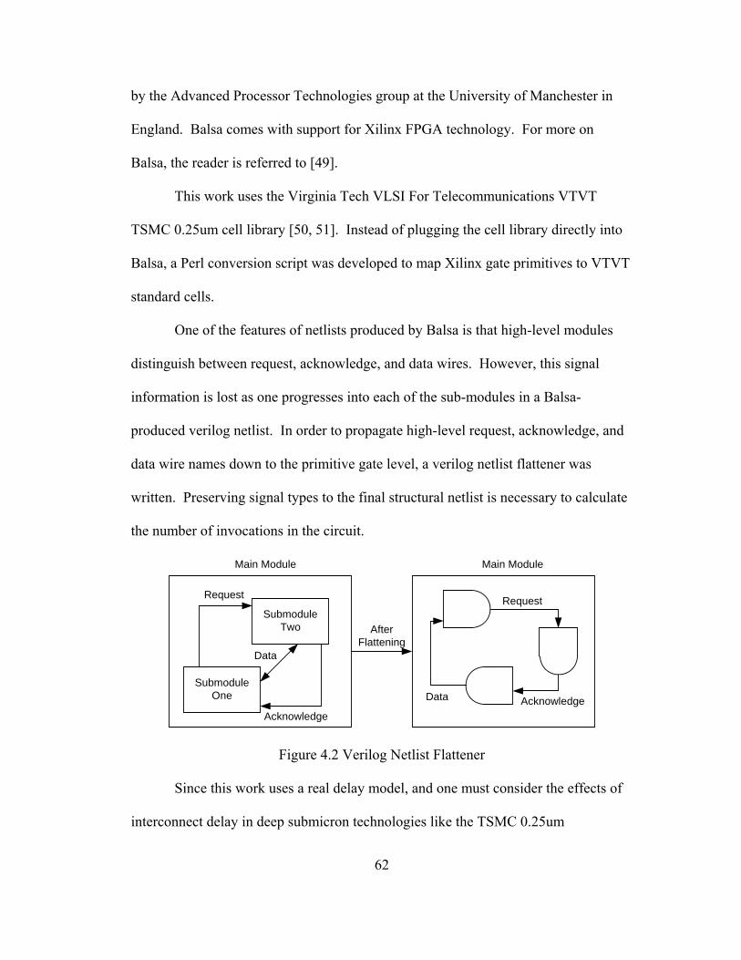
62
by the Advanced Processor Technologies group at the University of Manchester in
England. Balsa comes with support for Xilinx FPGA technology. For more on
Balsa, the reader is referred to [49].
This work uses the Virginia Tech VLSI For Telecommunications VTVT
TSMC 0.25um cell library [50, 51]. Instead of plugging the cell library directly into
Balsa, a Perl conversion script was developed to map Xilinx gate primitives to VTVT
standard cells.
One of the features of netlists produced by Balsa is that high-level modules
distinguish between request, acknowledge, and data wires. However, this signal
information is lost as one progresses into each of the sub-modules in a Balsa-
produced verilog netlist. In order to propagate high-level request, acknowledge, and
data wire names down to the primitive gate level, a verilog netlist flattener was
written. Preserving signal types to the final structural netlist is necessary to calculate
the number of invocations in the circuit.
SubmoduleOne
SubmoduleTwo
Request
Main Module
Acknowledge
Data
Main Module
Request
AcknowledgeData
AfterFlattening
Figure 4.2 Verilog Netlist Flattener
Since this work uses a real delay model, and one must consider the effects of
interconnect delay in deep submicron technologies like the TSMC 0.25um
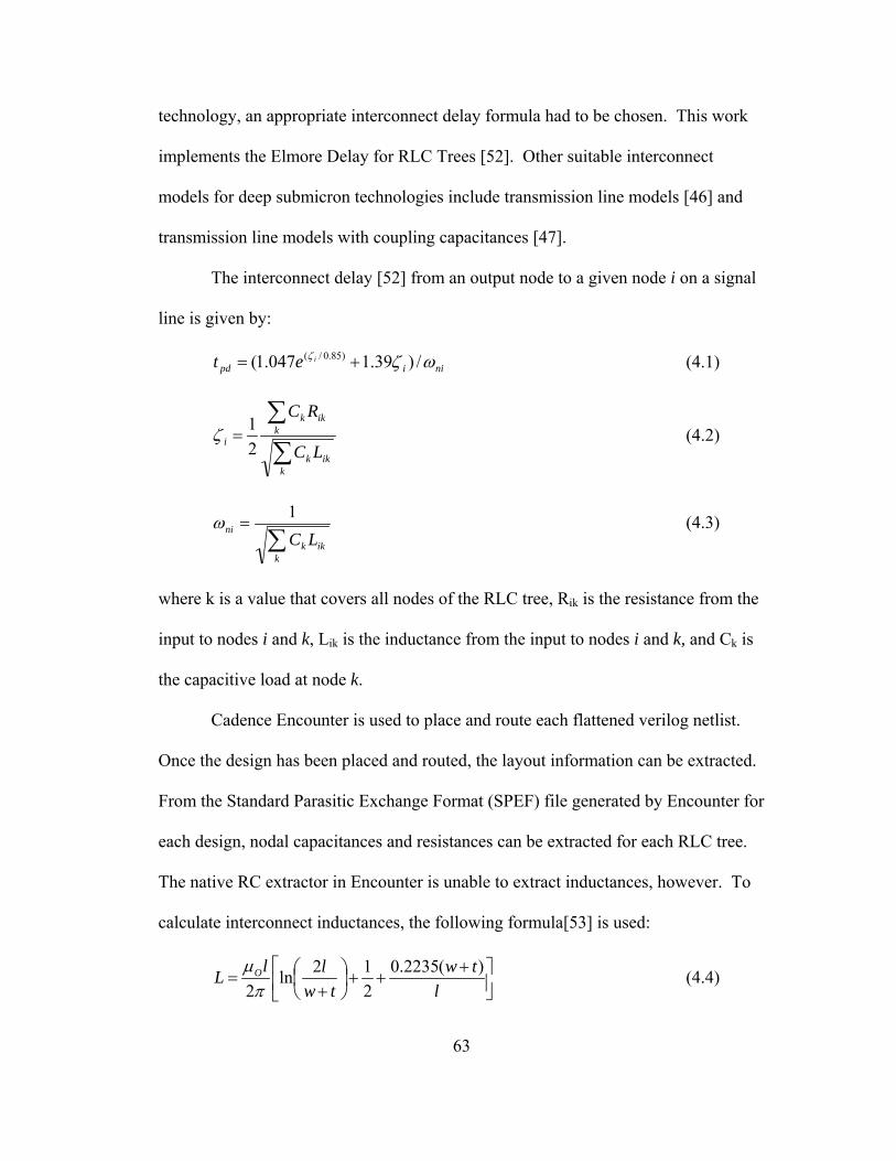
63
technology, an appropriate interconnect delay formula had to be chosen. This work
implements the Elmore Delay for RLC Trees [52]. Other suitable interconnect
models for deep submicron technologies include transmission line models [46] and
transmission line models with coupling capacitances [47].
The interconnect delay [52] from an output node to a given node i on a signal
line is given by:
niipdiet ωζζ /)39.1047.1( )85.0/( += (4.1)
∑
∑=
kikk
kikk
iLC
RC
21ζ (4.2)
∑
=
kikk
niLC
1ω (4.3)
where k is a value that covers all nodes of the RLC tree, Rik is the resistance from the
input to nodes i and k, Lik is the inductance from the input to nodes i and k, and Ck is
the capacitive load at node k.
Cadence Encounter is used to place and route each flattened verilog netlist.
Once the design has been placed and routed, the layout information can be extracted.
From the Standard Parasitic Exchange Format (SPEF) file generated by Encounter for
each design, nodal capacitances and resistances can be extracted for each RLC tree.
The native RC extractor in Encounter is unable to extract inductances, however. To
calculate interconnect inductances, the following formula[53] is used:
⎥⎦⎤+
++⎢⎣
⎡⎟⎠⎞
⎜⎝⎛
+=
ltw
twllL O )(2235.0
212ln
2πμ (4.4)

64
where Oμ is the permeability of free space, l is the length of the wire, w is the width
of the wire, and t is the thickness of the wire. To compute the length of the wire,
distance information for each net is extracted from the Design Exchange Format
(DEF) file generated by Encounter for each design. The width and thickness of a
wire is known from the technology file.
The intrinsic gate delays for each standard cell used in the design were
calculated using HSPICE. The delays were calculated assuming a standard capacitive
load of a FO4 inverter, which in this case equals 0.02 picofarads. The table below
shows the intrinsic gate delay for each standard cell utilized in picoseconds.
Table 4.1 Intrinsic Gate Delays
Intrinsic Gate DelaysCell Delay (ps)
BUF1 132 INV1 110
NAND2 114 NAND3 146 NAND4 190 AND2 159 AND3 201 AND4 263 NOR2 169 NOR3 248 NOR4 340 OR2 199 OR3 287 OR4 391 DRP 500
One assumption made in the implementation of HCAHPNs is that rise and fall
transition times are the same. In determining the instrinic gate delay for each
standard cell, both the rise and fall intrinsic gate delays were measured in HSPICE;
the greater of the two numbers was chosen to represent the intrinsic gate delay. The

65
gate delays incorporated into each HCAHPN primitive gate model represent the
worst-case intrinsic gate delay.
The CPN Processor is a software tool that accepts as input a flattened verilog
netlist, HCAHPN models for each primitive gate, and interconnect delay values for
each net and produces as output a corresponding HCAHPN in XML format that can
be simulated in CPN Tools. The CPN Processor also generates test vector inputs for
the CPN Tools simulator and the verilog testbench used by NCSim. The test vectors
are randomly generated sequences of binary values. Since each circuit simulated is
very small and has a limited number of inputs, a sequence of 10,000 input vectors for
each circuit is more than adequate to guarantee complete test coverage.
CPN Tools is a colored Petri net simulator developed by the CPN group at the
University of Aarhus in Denmark. It includes the ability to simulate both timed and
untimed colored Petri nets. With the ability to support hierarchical nets, complex
systems can be abstracted and simulated as a Petri net in CPN Tools.
The CPN Tools simulator accepts the Petri net generated by the CPN
Processor as well as input stimulus files in order to simulate a circuit. After
simulation of the Petri net is complete, the switching activity collected from the
monitors in CPN Tools is known for each gate. The collected switching activity and
load capacitance for each gate is used to calculate the amount of energy dissipated by
each gate over the course of circuit simulation.
As a reference point for the proposed energy estimation method, energy
estimates for each circuit were obtained from the gate-level power estimator in
Cadence PKS. The circuit was first simulated in NCSim using the same input vectors
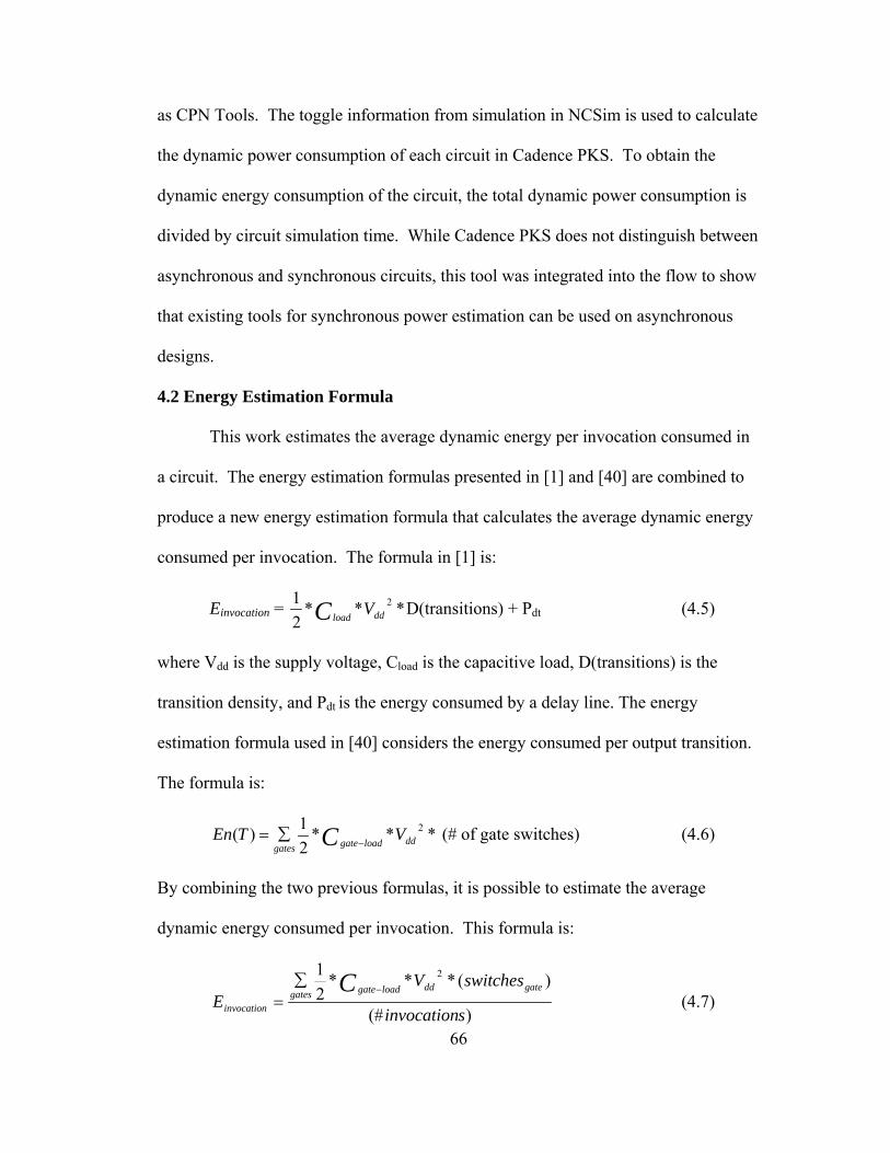
66
as CPN Tools. The toggle information from simulation in NCSim is used to calculate
the dynamic power consumption of each circuit in Cadence PKS. To obtain the
dynamic energy consumption of the circuit, the total dynamic power consumption is
divided by circuit simulation time. While Cadence PKS does not distinguish between
asynchronous and synchronous circuits, this tool was integrated into the flow to show
that existing tools for synchronous power estimation can be used on asynchronous
designs.
4.2 Energy Estimation Formula
This work estimates the average dynamic energy per invocation consumed in
a circuit. The energy estimation formulas presented in [1] and [40] are combined to
produce a new energy estimation formula that calculates the average dynamic energy
consumed per invocation. The formula in [1] is:
Einvocation = ***21 2
ddloadVC D(transitions) + Pdt (4.5)
where Vdd is the supply voltage, Cload is the capacitive load, D(transitions) is the
transition density, and Pdt is the energy consumed by a delay line. The energy
estimation formula used in [40] considers the energy consumed per output transition.
The formula is:
***21)( 2
ddloadgategatesVTEn C −
∑= (# of gate switches) (4.6)
By combining the two previous formulas, it is possible to estimate the average
dynamic energy consumed per invocation. This formula is:
)(#
)(***21 2
sinvocation
switchesVE
gateddloadgategatesinvocation
C −∑
= (4.7)

67
where C loadgate− is the capacitive output load of a gate, ddV is the supply voltage,
gateswitches is the number of times the output of a gate has switched, and
sinvocation# is the total number of completed request/acknowledge handshake pairs.
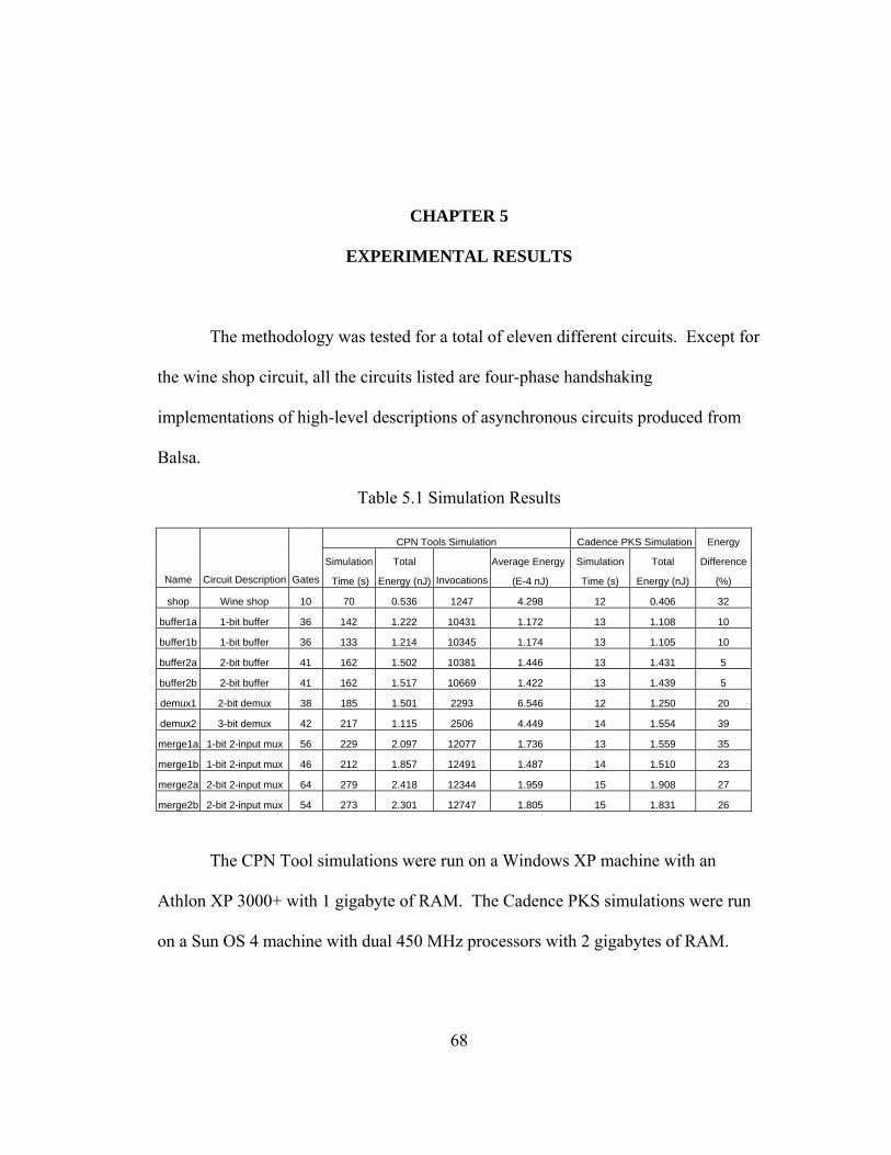
68
CHAPTER 5
EXPERIMENTAL RESULTS
The methodology was tested for a total of eleven different circuits. Except for
the wine shop circuit, all the circuits listed are four-phase handshaking
implementations of high-level descriptions of asynchronous circuits produced from
Balsa.
Table 5.1 Simulation Results
CPN Tools Simulation Cadence PKS Simulation Energy
Simulation Total Average Energy Simulation Total Difference
Name Circuit Description Gates Time (s) Energy (nJ) Invocations (E-4 nJ) Time (s) Energy (nJ) (%)
shop Wine shop 10 70 0.536 1247 4.298 12 0.406 32
buffer1a 1-bit buffer 36 142 1.222 10431 1.172 13 1.108 10
buffer1b 1-bit buffer 36 133 1.214 10345 1.174 13 1.105 10
buffer2a 2-bit buffer 41 162 1.502 10381 1.446 13 1.431 5
buffer2b 2-bit buffer 41 162 1.517 10669 1.422 13 1.439 5
demux1 2-bit demux 38 185 1.501 2293 6.546 12 1.250 20
demux2 3-bit demux 42 217 1.115 2506 4.449 14 1.554 39
merge1a 1-bit 2-input mux 56 229 2.097 12077 1.736 13 1.559 35
merge1b 1-bit 2-input mux 46 212 1.857 12491 1.487 14 1.510 23
merge2a 2-bit 2-input mux 64 279 2.418 12344 1.959 15 1.908 27
merge2b 2-bit 2-input mux 54 273 2.301 12747 1.805 15 1.831 26
The CPN Tool simulations were run on a Windows XP machine with an
Athlon XP 3000+ with 1 gigabyte of RAM. The Cadence PKS simulations were run
on a Sun OS 4 machine with dual 450 MHz processors with 2 gigabytes of RAM.

69
During simulation in CPN Tools, the switching activity for each gate as well
as the number of acknowledge and requests in the circuit are recorded. This activity
is used to calculate the amount of energy dissipated by each gate as well as the
number of total invocations in the circuit. For each circuit, a set of 10,000 random
binary input vectors was generated. The same test vectors were used in CPN Tool
simulation and Cadence PKS simulation. For both simulation tools, the time between
different input vectors was set to 500 ps. There is a wide variation in the results for
energy consumption between CPN Tools and Cadence PKS. While CPN Tools uses
the actual capacitance from layout, Cadence PKS uses information from the
technology library to estimate the load capacitance. These two different methods of
calculating load capacitance can explain the wide variation of results between the two
simulators.
One major limitation of the current version of CPN Tools is that it stalls on
syntax checking on large numbers of monitors. Since the monitoring functionality of
CPN Tools is used to record the switching activity of each gate, the number of
monitors in a simulation is a function of the number of gates within a circuit. The
largest design CPN Tools was able to syntax check successfully was merge2a, which
is 64 gates; the simulator stalled on syntax checking of a 74 gate two-bit
asynchronous shifter. Without monitoring functionality present, CPN Tools was able
to complete the loading of Petri nets with several hundred gates. Once this limitation
is corrected in future versions of CPN Tools, the methodology should be able to work
with designs ranging from hundreds to thousands of gates.

70
While interconnect delay is considered in the simulation of the circuits, the
delay effects are negligible due to the very small circuit sizes. Once the major
limitation of CPN Tools is corrected, the effects of interconnect delay would be
clearly seen as circuits scale into the hundreds and thousands of gates.
In this thesis, the objective was to develop a framework for Petri net modeling
of asynchronous circuits for energy estimation. Thus, we have developed new
models for asynchronous gates and circuits, developed a complete framework and
tool flow for energy estimation, and implemented the proposed tool using CPN Tools.
The use of CPN Tools is only to show proof of concept by implementing a
customized software tool based on our proposed methodology with results in a time
efficient tool that can handle large circuits. A practical tool needs to be built in the
future for use in asynchronous circuit design environment.
71
CHAPTER 6
CONCLUSIONS
This work is the first to do simulative gate-level energy estimation of
asynchronous circuits. This work also includes a real-delay model to capture the
effects of glitch power. While interconnect delay was negligible next to gate delay in
the very small circuits that were tested, once larger circuits with hundreds and
thousands of gates can be tested, one would clearly see the effects of interconnect
delay and glitch power.
Once the limitation in CPN Tools has been corrected, larger designs of several
hundred and even thousands of gates could be simulated. While test vector
generation for exhaustive simulation of a circuit is not a problem given the very small
circuit sizes that were simulated, it does become a problem with designs that range in
the hundreds and thousands of gates. Future work could include state space
exploration to produce appropriate test vectors.
CPN Tools has been designed for many uses. Many different types of systems
can be modeled as HCPNs, which CPN Tools has the capability to simulate. In its
current state, however, CPN Tools is inefficient for hardware simulation.
The proposed methodology is only suitable for asynchronous circuit
implementations that use handshaking communication on distinct request and

72
acknowledge signal lines. For timed asynchronous circuit implementations that
combine request and acknowledge channels into one signal wire, the proposed
methodology is not suitable for energy estimation.
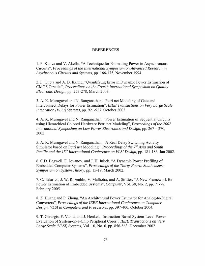
73
REFERENCES
1. P. Kudva and V. Akella, “A Technique for Estimating Power in Asynchronous Circuits”, Proceedings of the International Symposium on Advanced Research in Asychronous Circuits and Systems, pp. 166-175, November 1994. 2. P. Gupta and A. B. Kahng, “Quantifying Error in Dynamic Power Estimation of CMOS Circuits”, Proceedings on the Fourth International Symposium on Quality Electronic Design, pp. 273-278, March 2003. 3. A. K. Murugavel and N. Ranganathan, “Petri net Modeling of Gate and Interconnect Delays for Power Estimation”, IEEE Transactions on Very Large Scale Integration (VLSI) Systems, pp. 921-927, October 2003. 4. A. K. Murugavel and N. Ranganathan, “Power Estimation of Sequential Circuits using Hierarchical Colored Hardware Petri net Modeling”, Proceedings of the 2002 International Symposium on Low Power Electronics and Design, pp. 267 – 270, 2002. 5. A. K. Murugavel and N. Ranganathan, “A Real Delay Switching Activity Simulator based on Petri net Modeling”, Proceedings of the 7th Asia and South Pacific and the 15th International Conference on VLSI Design, pp. 181-186, Jan 2002. 6. C.D. Bagwell, E. Jovanov, and J. H. Julick, “A Dynamic Power Profiling of Embedded Computer Systems”, Proceedings of the Thirty-Fourth Southeastern Symposium on System Theory, pp. 15-19, March 2002. 7. C. Talarico, J. W. Rozenblit, V. Malhotra, and A. Stritter, “A New Framework for Power Estimation of Embedded Systems”, Computer, Vol. 38, No. 2, pp. 71-78, February 2005. 8. Z. Huang and P. Zhong, “An Architectural Power Estimator for Analog-to-Digital Converters”, Proceedings of the IEEE International Conference on Computer Design: VLSI in Computers and Processors, pp. 397-400, October 2004. 9. T. Givargis, F. Vahid, and J. Henkel, “Instruction-Based System-Level Power Evaluation of System-on-a-Chip Peripheral Cores”, IEEE Transactions on Very Large Scale (VLSI) Systems, Vol. 10, No. 6, pp. 856-863, December 2002.
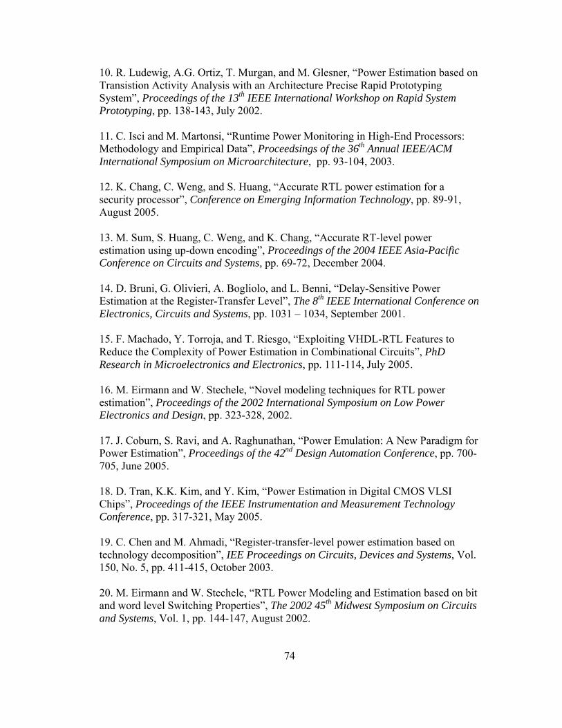
74
10. R. Ludewig, A.G. Ortiz, T. Murgan, and M. Glesner, “Power Estimation based on Transistion Activity Analysis with an Architecture Precise Rapid Prototyping System”, Proceedings of the 13th IEEE International Workshop on Rapid System Prototyping, pp. 138-143, July 2002. 11. C. Isci and M. Martonsi, “Runtime Power Monitoring in High-End Processors: Methodology and Empirical Data”, Proceedsings of the 36th Annual IEEE/ACM International Symposium on Microarchitecture, pp. 93-104, 2003. 12. K. Chang, C. Weng, and S. Huang, “Accurate RTL power estimation for a security processor”, Conference on Emerging Information Technology, pp. 89-91, August 2005. 13. M. Sum, S. Huang, C. Weng, and K. Chang, “Accurate RT-level power estimation using up-down encoding”, Proceedings of the 2004 IEEE Asia-Pacific Conference on Circuits and Systems, pp. 69-72, December 2004. 14. D. Bruni, G. Olivieri, A. Bogliolo, and L. Benni, “Delay-Sensitive Power Estimation at the Register-Transfer Level”, The 8th IEEE International Conference on Electronics, Circuits and Systems, pp. 1031 – 1034, September 2001. 15. F. Machado, Y. Torroja, and T. Riesgo, “Exploiting VHDL-RTL Features to Reduce the Complexity of Power Estimation in Combinational Circuits”, PhD Research in Microelectronics and Electronics, pp. 111-114, July 2005. 16. M. Eirmann and W. Stechele, “Novel modeling techniques for RTL power estimation”, Proceedings of the 2002 International Symposium on Low Power Electronics and Design, pp. 323-328, 2002. 17. J. Coburn, S. Ravi, and A. Raghunathan, “Power Emulation: A New Paradigm for Power Estimation”, Proceedings of the 42nd Design Automation Conference, pp. 700-705, June 2005. 18. D. Tran, K.K. Kim, and Y. Kim, “Power Estimation in Digital CMOS VLSI Chips”, Proceedings of the IEEE Instrumentation and Measurement Technology Conference, pp. 317-321, May 2005. 19. C. Chen and M. Ahmadi, “Register-transfer-level power estimation based on technology decomposition”, IEE Proceedings on Circuits, Devices and Systems, Vol. 150, No. 5, pp. 411-415, October 2003. 20. M. Eirmann and W. Stechele, “RTL Power Modeling and Estimation based on bit and word level Switching Properties”, The 2002 45th Midwest Symposium on Circuits and Systems, Vol. 1, pp. 144-147, August 2002.
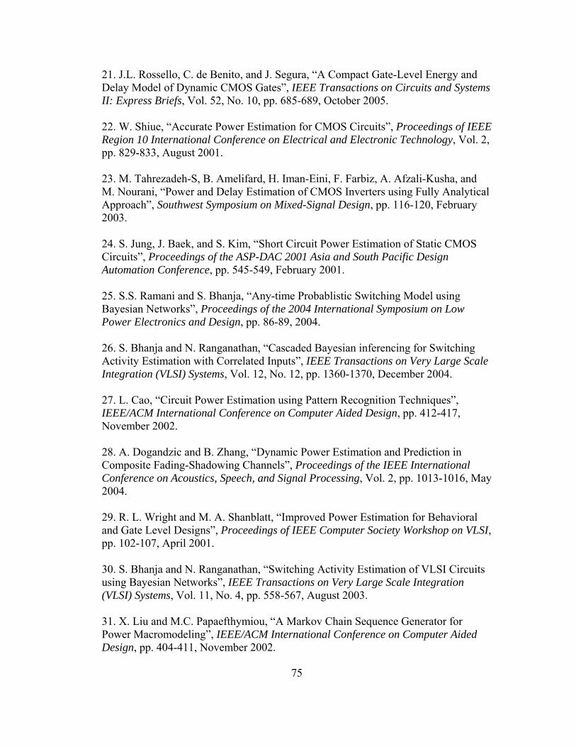
75
21. J.L. Rossello, C. de Benito, and J. Segura, “A Compact Gate-Level Energy and Delay Model of Dynamic CMOS Gates”, IEEE Transactions on Circuits and Systems II: Express Briefs, Vol. 52, No. 10, pp. 685-689, October 2005. 22. W. Shiue, “Accurate Power Estimation for CMOS Circuits”, Proceedings of IEEE Region 10 International Conference on Electrical and Electronic Technology, Vol. 2, pp. 829-833, August 2001. 23. M. Tahrezadeh-S, B. Amelifard, H. Iman-Eini, F. Farbiz, A. Afzali-Kusha, and M. Nourani, “Power and Delay Estimation of CMOS Inverters using Fully Analytical Approach”, Southwest Symposium on Mixed-Signal Design, pp. 116-120, February 2003. 24. S. Jung, J. Baek, and S. Kim, “Short Circuit Power Estimation of Static CMOS Circuits”, Proceedings of the ASP-DAC 2001 Asia and South Pacific Design Automation Conference, pp. 545-549, February 2001. 25. S.S. Ramani and S. Bhanja, “Any-time Probablistic Switching Model using Bayesian Networks”, Proceedings of the 2004 International Symposium on Low Power Electronics and Design, pp. 86-89, 2004. 26. S. Bhanja and N. Ranganathan, “Cascaded Bayesian inferencing for Switching Activity Estimation with Correlated Inputs”, IEEE Transactions on Very Large Scale Integration (VLSI) Systems, Vol. 12, No. 12, pp. 1360-1370, December 2004. 27. L. Cao, “Circuit Power Estimation using Pattern Recognition Techniques”, IEEE/ACM International Conference on Computer Aided Design, pp. 412-417, November 2002. 28. A. Dogandzic and B. Zhang, “Dynamic Power Estimation and Prediction in Composite Fading-Shadowing Channels”, Proceedings of the IEEE International Conference on Acoustics, Speech, and Signal Processing, Vol. 2, pp. 1013-1016, May 2004. 29. R. L. Wright and M. A. Shanblatt, “Improved Power Estimation for Behavioral and Gate Level Designs”, Proceedings of IEEE Computer Society Workshop on VLSI, pp. 102-107, April 2001. 30. S. Bhanja and N. Ranganathan, “Switching Activity Estimation of VLSI Circuits using Bayesian Networks”, IEEE Transactions on Very Large Scale Integration (VLSI) Systems, Vol. 11, No. 4, pp. 558-567, August 2003. 31. X. Liu and M.C. Papaefthymiou, “A Markov Chain Sequence Generator for Power Macromodeling”, IEEE/ACM International Conference on Computer Aided Design, pp. 404-411, November 2002.
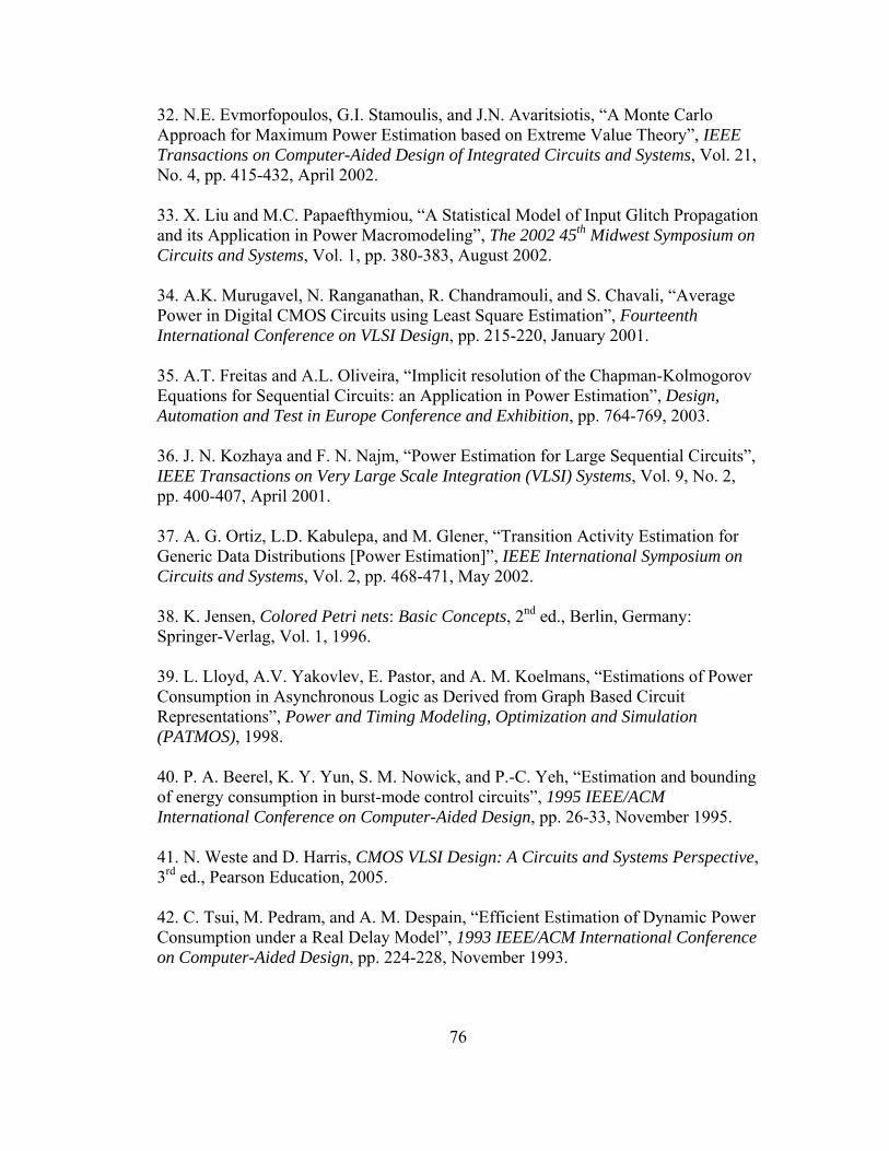
76
32. N.E. Evmorfopoulos, G.I. Stamoulis, and J.N. Avaritsiotis, “A Monte Carlo Approach for Maximum Power Estimation based on Extreme Value Theory”, IEEE Transactions on Computer-Aided Design of Integrated Circuits and Systems, Vol. 21, No. 4, pp. 415-432, April 2002. 33. X. Liu and M.C. Papaefthymiou, “A Statistical Model of Input Glitch Propagation and its Application in Power Macromodeling”, The 2002 45th Midwest Symposium on Circuits and Systems, Vol. 1, pp. 380-383, August 2002. 34. A.K. Murugavel, N. Ranganathan, R. Chandramouli, and S. Chavali, “Average Power in Digital CMOS Circuits using Least Square Estimation”, Fourteenth International Conference on VLSI Design, pp. 215-220, January 2001. 35. A.T. Freitas and A.L. Oliveira, “Implicit resolution of the Chapman-Kolmogorov Equations for Sequential Circuits: an Application in Power Estimation”, Design, Automation and Test in Europe Conference and Exhibition, pp. 764-769, 2003. 36. J. N. Kozhaya and F. N. Najm, “Power Estimation for Large Sequential Circuits”, IEEE Transactions on Very Large Scale Integration (VLSI) Systems, Vol. 9, No. 2, pp. 400-407, April 2001. 37. A. G. Ortiz, L.D. Kabulepa, and M. Glener, “Transition Activity Estimation for Generic Data Distributions [Power Estimation]”, IEEE International Symposium on Circuits and Systems, Vol. 2, pp. 468-471, May 2002. 38. K. Jensen, Colored Petri nets: Basic Concepts, 2nd ed., Berlin, Germany: Springer-Verlag, Vol. 1, 1996. 39. L. Lloyd, A.V. Yakovlev, E. Pastor, and A. M. Koelmans, “Estimations of Power Consumption in Asynchronous Logic as Derived from Graph Based Circuit Representations”, Power and Timing Modeling, Optimization and Simulation (PATMOS), 1998. 40. P. A. Beerel, K. Y. Yun, S. M. Nowick, and P.-C. Yeh, “Estimation and bounding of energy consumption in burst-mode control circuits”, 1995 IEEE/ACM International Conference on Computer-Aided Design, pp. 26-33, November 1995. 41. N. Weste and D. Harris, CMOS VLSI Design: A Circuits and Systems Perspective, 3rd ed., Pearson Education, 2005. 42. C. Tsui, M. Pedram, and A. M. Despain, “Efficient Estimation of Dynamic Power Consumption under a Real Delay Model”, 1993 IEEE/ACM International Conference on Computer-Aided Design, pp. 224-228, November 1993.
77
43. T. Chou and K. Roy, “Estimation of Activity for Static and Domino CMOS Circuits Considering Signal Correlations and Simultaneous Switching”, IEEE Transactions on Computer-Aided Design of Integrated Circuits and Systems, Vol. 15, No. 10, pp. 1257-1265, October 1996. 44. K.M. Buyuksahin and F.N. Najm, “High-level power estimation with interconnect effects”, Proceedings of the 2000 International Symposium on Low Power Electronics and Design, pp. 197-202, 2000. 45. R. Marculescu, D. Marculescu, and M. Pedram, “Switching Activity Analysis Considering Spatiotemporal Correlations”, 1994 IEEE/ACM International Conference on Computer-Aided Design, pp. 294-299, November 1994. 46. T.-C. Chen, S.-R. Pan, and Y.-W. Chang, “Timing Modeling and Optimization under the Transmission Line Model,” IEEE Transactions on VLSI Systems, vol. 12, no. 1, pp. 28-41, January 2004. 47. N. Hanchate and N. Ranganathan, “Simultaneous Interconnect Delay and Crosstalk Noise Optimization through Gate Sizing Using Game Theory”, IEEE Transactions on Computers, vol. 55, No. 8, pp. 1011-1023, August 2006. 48. P.A. Beerel, C. Hsieh, and S. Wadekar, “Estimation of Energy Consumption in Speed-Independent Control Circuits,” IEEE Transactions on Computer-Aided Design of Integrated Circuits and Systems, vol. 15, No. 6, pp. 672-680, June 1996. 49. A. Bardsley. The Balsa web pages. http://intranet.cs.man.ac.uk/apt/projects/tools/balsa/. 50. J. B. Sulistyo, J. Perry, and D. S. Ha, " Developing Standard Cells for TSMC 0.25um Technology under MOSIS DEEP Rules", Department of Electrical and Computer Engineering, Virginia Tech, Technical Report VISC-2003-01, November 2003.
51. J. B. Sulistyo and D. S. Ha, "A New Characterization Method for Delay and Power Dissipation of Standard Library Cells", VLSI Design, Vol. 15, No. 3, pp. 667-678, 2002.
52. Y. I. Ismail, E.G. Friedman, and J. L. Neves, “Equivalent Elmore delay for RLC trees,” IEEE Transactions on Computer-Aided Design of Integrated Circuits and Systems, vol. 19, No. 1, pp. 83-97, January 2000. 53. F. Grover, Inductance Calculations Working Formulas and Tables, Instrum. Soc. Of America, 1945.

78
54. C. J. Myers, Asynchronous Circuit Design, New York: John Wiley & Sons Inc., 2001. 55. K. Jensen. “An introduction to the theoretical aspects of colored petri nets.” Advances in Petri nets, Ed. J.W. Bakker; W.-P. de Roever; G. Rozenberg, LCNS 803 (1993), pp. 203-272, 1993. 56. International Road-map Committee. International Technology Road-map for Semiconductors, 2006 update edition, 2006. 57. D. McFarland, Cell Phone Ownership Grows 29 Percent from 1999-2001, Scarborough Research. 18 March 2002. 58. S.B. Furber, J.D. Garside, P. Riocreux, S. Temple, P. Day, L. Jianwei, and N.C. Paver, “AMULET2e: an asynchronous embedded controller,” Proceedings of the Third International Symposium on Advanced Research in Asynchronous Circuits and Systems, 1997, pp. 290-299, 7-10 April 1997. 59. S. Rotem, K. Stevens, R. Ginosar, P. Beerel, C. Myers, K. Yun, R. Kol, C. Dike, M. Roncken, and B. Agapiev, “RAPPID: an asynchronous instruction length decoder,” Proceedings of the Fifth International Symposium on Advanced Research in Asynchronous Circuits and Systems, 1999, pp.60-79, 1999. 60. P.L. Penzes and A. J. Martin, “An energy estimation method for asynchronous circuits with application to an asynchronous microprocessor,” Proceedings of the 2002 Design, Automation, and Test in Europe Conference and Exhibition, pp. 640-647, 4-8 March 2002. 61. M. Salehi, K. Saleh, H. Kalantari, M. Naderi, and H. Pedram, “High-level energy estimation of template-based QDI asynchronous circuits based on transition counting,” ICM 2004 - Proceedings of the 16th International Conference on Microelectronics, 2004, pp. 489-492, 6-8 Dec. 2004. 62. M. Niknahad, B. Ghavami, M. Najibi, and H. Pedram, “A Power Estimation Methodology for QDI Asynchronous Circuits based on High-Level Simulation,” IEEE Computer Society Annual Symposium on VLSI, 2007, pp. 471-472, March 2007.


![InTech-Control and Estimation of Asynchronous Machines Using Fuzzy Logic[1]](https://img.dokumen.tips/doc/110x75/577cd8961a28ab9e78a18997/intech-control-and-estimation-of-asynchronous-machines-using-fuzzy-logic1.jpg)