Embed Size (px)
Citation preview
CORP IR/May 13, 2011
FY2012 Financial Forecast and
Management Policy
Hiroshi Takenaka, President & CEO
May 13, 2011
FY2011 Review
CORP IR/May 13, 2011
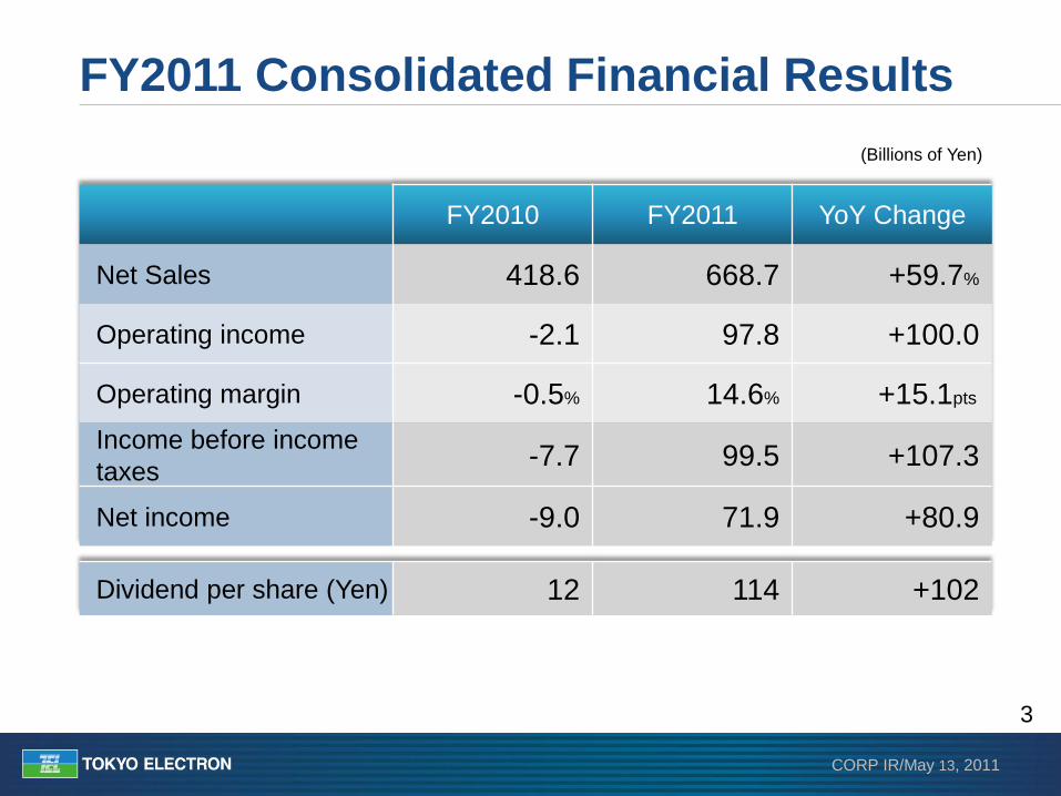
3
FY2010 FY2011 YoY Change
Net Sales 418.6 668.7 +59.7%
Operating income -2.1 97.8 +100.0
Operating margin -0.5% 14.6% +15.1pts
Income before income
taxes -7.7 99.5 +107.3
Net income -9.0 71.9 +80.9
Dividend per share (Yen) 12 114 +102
FY2011 Consolidated Financial Results
(Billions of Yen)

CORP IR/May 13, 2011
4
FY2011 Results
▶ Net sales ¥668.7 billion, up 59.7%
▶ Operating income ¥97.8 billion, up ¥100 billion
▶ Profitability improved
• Gross profit margin: 35.1%
• SPE segment pre-tax profit margin: 23.6%
▶ R&D expenses: ¥70.5 billion, record level
▶ Operating cash flow: ¥83.2 billion generated
▶ Executing production facility strategy
• Started construction of new Miyagi Plant
• Decided to construct new plant in Kunshan City, Jiangsu Province, China
CORP IR/May 13, 2011
5
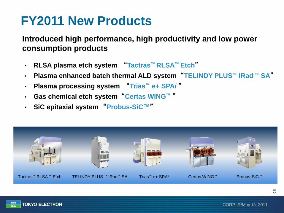
FY2011 New Products
• RLSA plasma etch system “Tactras™ RLSA™ Etch”
• Plasma enhanced batch thermal ALD system “TELINDY PLUS™ IRad ™ SA”
• Plasma processing system “Trias™ e+ SPAi ”
• Gas chemical etch system “Certas WING™ ”
• SiC epitaxial system “Probus-SiC™”
Introduced high performance, high productivity and low power
consumption products
Tactras™ RLSA ™ Etch TELINDY PLUS ™ IRad™ SA Trias™ e+ SPAi Certas WING™ Probus-SiC ™
Business Environment
CORP IR/May 13, 2011
7 FPD: Flat Panel Display PV: Photovoltaic Cell
CY2011 Business Environment
▶ SPE capex Although 1st first half capex is expected to be slightly below the initial
forecast due to the effects of the Japan earthquake, expecting increase in
2nd half. Because investments for NAND, Logic/Foundry are still strong,
overall capex for the year is expected to increase 10%.
▶ FPD capex Although large panel investment in adjustment phase, small and mid-sized
panel investment for smartphones is strong and overall capex expected to
be about same level as 2010
▶ PV capex
Currently, single crystal silicon and Cd-Te strong, good future potential for
thin-film silicon as conversion efficiency improves

CORP IR/May 13, 2011
8
0
10
20
30
40
2006 2007 2008 2009 2010 2011E
($B)
CY2011 WFE CAPEX by Application
34.1B
Investments for NAND & Logic/Foundry are expanding
Source: Gartner Dataquest, TEL
DRAM -35%
NAND +34%
Logic/Foundry
+27%

CORP IR/May 13, 2011
9
Quarterly Orders
0
50
100
150
200
250
300
00/7
-9
10-1
2
01/1
-3
4-6
7-9
10-1
2
02/1
-3
4-6
7-9
10-1
2
03/1
-3
4-6
7-9
10-1
2
04/1
-3
4-6
7-9
10-1
2
05/1
-3
4-6
7-9
10-1
2
06/1
-3
4-6
7-9
10-1
2
07/1
-3
4-6
7-9
10-1
2
08/1
-3
4-6
7-9
10-1
2
09/1
-3
4-6
7-9
10-1
2
10/1
-3
4-6
7-9
10-1
2
11/1
-3
SPE Order FPD/PVE Order
(Billions of yen) Jan-Mar/2011
SPE 155.8(+21%)
FPD/PVE 26.3(+73%)
Total: 182.1(+27%) ( ): change from Oct-Dec/2010
% is calculated using full amounts
CORP IR/May 13, 2011
10
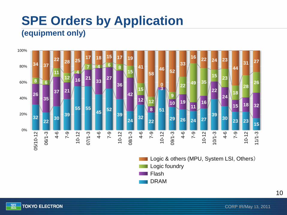
SPE Orders by Application (equipment only)
32 22
30 39
55 55 45
52 39
24 32
22
51
29 26 24 27 39
30 23 23
15
26 35
37 21
16 21 33
27
36
42 12
8
3
10 19 11
16
22
24
15 18 32
8 6
11 12
4 7 4 6
8 15
15
12
0
9
22 49 35
15 23
18
28 26
34 37
22 28 25
17 18 15 17 19
41
58 46
52
33
16 22 24 23
44 31 27
0%
20%
40%
60%
80%
100%
05/1
0-1
2
06/1
-3
4-6
7-9
10-1
2
07/1
-3
4-6
7-9
10-1
2
08/1
-3
4-6
7-9
10-1
2
09/1
-3
4-6
7-9
10-1
2
10/1
-3
4-6
7-9
10-1
2
11/1
-3
DRAM
Flash
Logic foundry
Logic & others (MPU, System LSI, Others)
FY2012 Financial Estimates
CORP IR/May 13, 2011
12
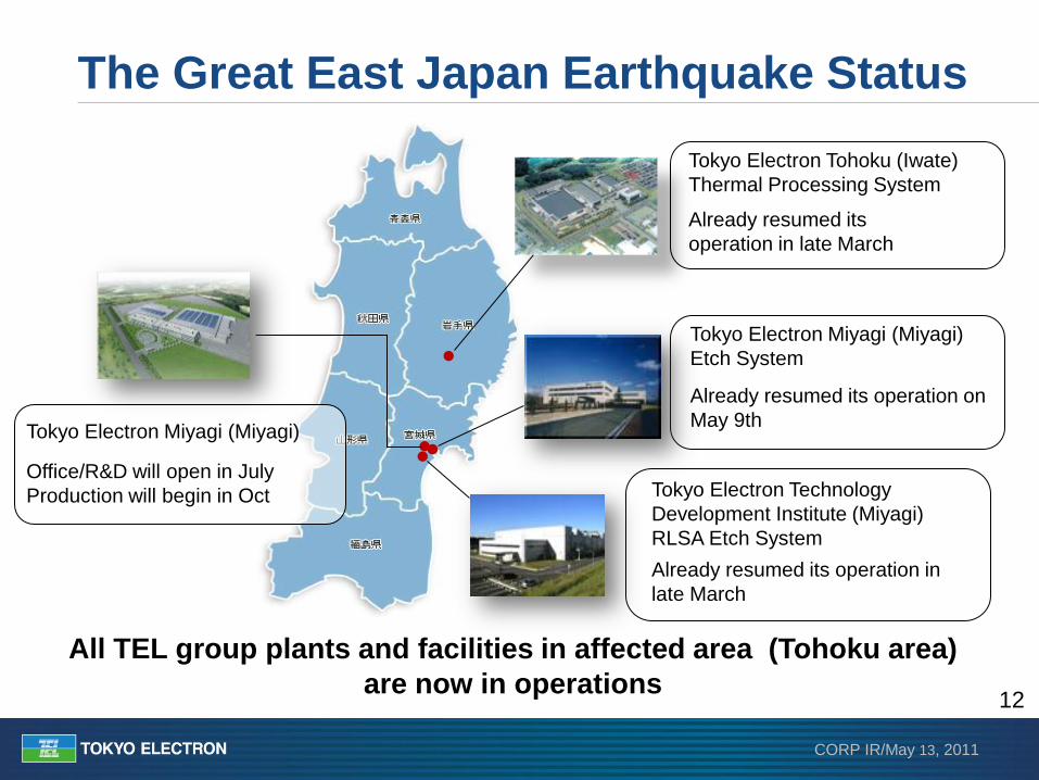
Tokyo Electron Tohoku (Iwate)
Thermal Processing System
Tokyo Electron Technology
Development Institute (Miyagi)
RLSA Etch System
Tokyo Electron Miyagi (Miyagi)
Etch System
Already resumed its
operation in late March
Already resumed its operation in
late March
Already resumed its operation on
May 9th
The Great East Japan Earthquake Status
All TEL group plants and facilities in affected area (Tohoku area)
are now in operations
Office/R&D will open in July
Production will begin in Oct
Tokyo Electron Miyagi (Miyagi)
CORP IR/May 13, 2011
13
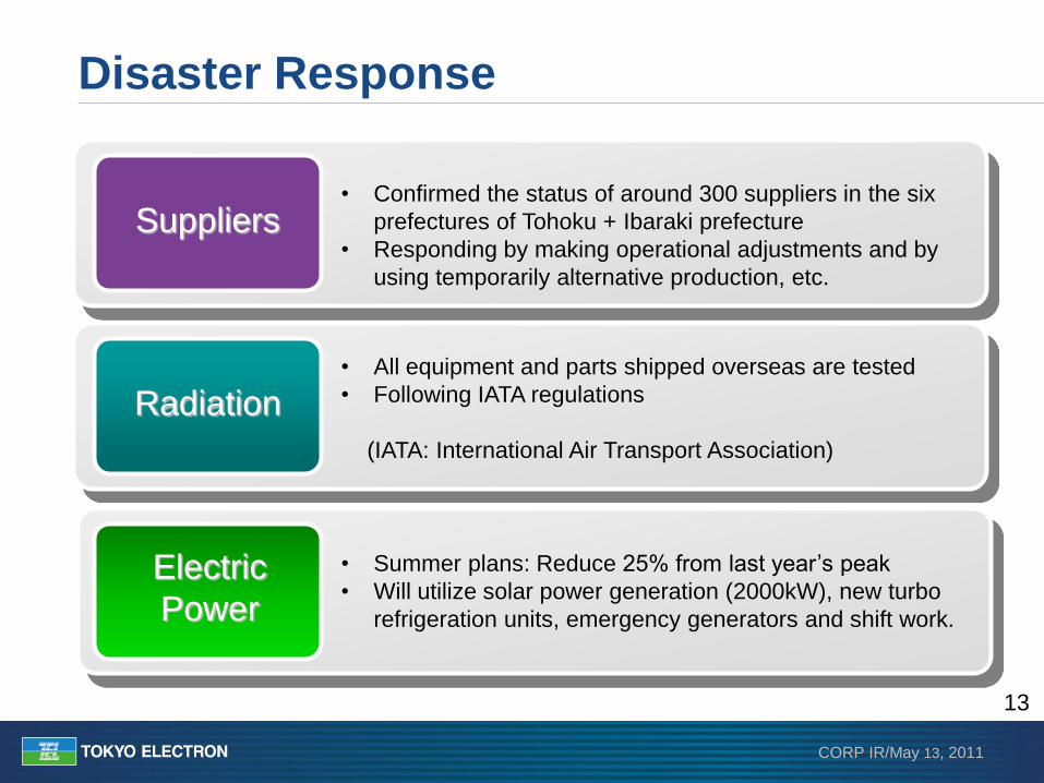
Disaster Response
Suppliers • Confirmed the status of around 300 suppliers in the six
prefectures of Tohoku + Ibaraki prefecture
• Responding by making operational adjustments and by
using temporarily alternative production, etc.
Radiation • All equipment and parts shipped overseas are tested
• Following IATA regulations
(IATA: International Air Transport Association)
Electric
Power
• Summer plans: Reduce 25% from last year’s peak
• Will utilize solar power generation (2000kW), new turbo
refrigeration units, emergency generators and shift work.
CORP IR/May 13, 2011
14
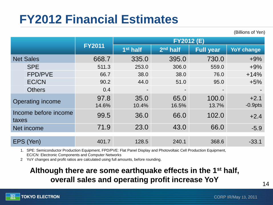
FY2012 Financial Estimates
FY2011 FY2012 (E)
1st half 2nd half Full year YoY change
Net Sales 668.7 335.0 395.0 730.0 +9%
SPE 511.3 253.0 306.0 559.0 +9%
FPD/PVE 66.7 38.0 38.0 76.0 +14%
EC/CN 90.2 44.0 51.0 95.0 +5%
Others 0.4 - - - -
Operating income 97.8
14.6%
35.0 10.4%
65.0 16.5%
100.0 13.7%
+2.1 -0.9pts
Income before income
taxes 99.5 36.0 66.0 102.0 +2.4
Net income 71.9 23.0 43.0 66.0 -5.9
EPS (Yen) 401.7 128.5 240.1 368.6 -33.1
1. SPE: Semiconductor Production Equipment, FPD/PVE: Flat Panel Display and Photovoltaic Cell Production Equipment,
EC/CN: Electronic Components and Computer Networks
2 YoY changes and profit ratios are calculated using full amounts, before rounding.
(Billions of Yen)
Although there are some earthquake effects in the 1st half,
overall sales and operating profit increase YoY
CORP IR/May 13, 2011
15
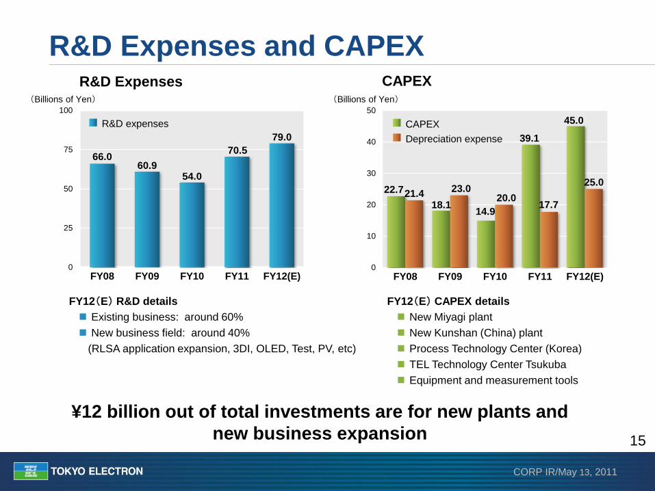
R&D Expenses and CAPEX
66.0 60.9
54.0
70.5
79.0
0
25
50
75
100
FY08 FY09 FY10 FY11 FY12(E)
22.7
18.1 14.9
39.1
45.0
21.4 23.0
20.0 17.7
25.0
0
10
20
30
40
50
FY08 FY09 FY10 FY11 FY12(E)
FY12(E) R&D details
Existing business: around 60%
New business field: around 40%
(RLSA application expansion, 3DI, OLED, Test, PV, etc)
¥12 billion out of total investments are for new plants and
new business expansion
CAPEX R&D Expenses (Billions of Yen) (Billions of Yen)
FY12(E) CAPEX details
New Miyagi plant
New Kunshan (China) plant
Process Technology Center (Korea)
TEL Technology Center Tsukuba
Equipment and measurement tools
R&D expenses CAPEX
Depreciation expense

CORP IR/May 13, 2011
16
Dividend payout ratio 35.3%, expecting dividend per share increase
FY12 Dividend Forecast
38
8 8 10
45 55
103
125
24 12
114
130
0
50
100
150
FY01 FY02 FY03 FY04 FY05 FY06 FY07 FY08 FY09 FY10 FY11 FY12
(Forecast)
Dividend per share (E)
Interim Year-end Year total
¥45 ¥85 ¥130
(Yen)
*Changed dividend payout ratio from 20% to 35% from FY11 year end dividend.
CORP IR/May 13, 2011
17
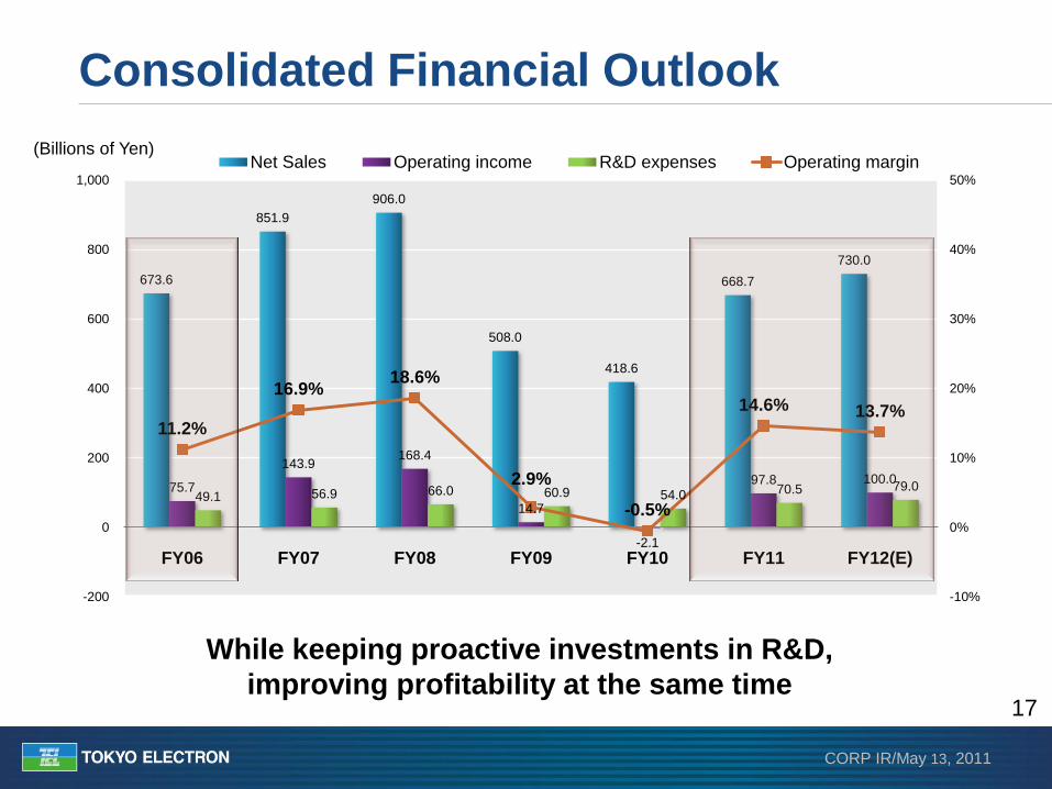
Consolidated Financial Outlook
673.6
851.9
906.0
508.0
418.6
668.7
730.0
75.7
143.9 168.4
14.7
-2.1
97.8 100.0
49.1 56.9 66.0 60.9 54.0 70.5 79.0
11.2%
16.9% 18.6%
2.9%
-0.5%
14.6% 13.7%
-10%
0%
10%
20%
30%
40%
50%
-200
0
200
400
600
800
1,000
FY06 FY07 FY08 FY09 FY10 FY11 FY12(E)
(Billions of Yen) Net Sales Operating income R&D expenses Operating margin
While keeping proactive investments in R&D,
improving profitability at the same time
Management Policy
CORP IR/May 13, 2011
19
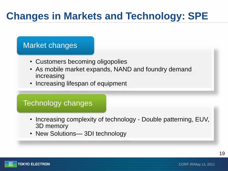
Changes in Markets and Technology: SPE
• Customers becoming oligopolies
• As mobile market expands, NAND and foundry demand increasing
• Increasing lifespan of equipment
Market changes
• Increasing complexity of technology - Double patterning, EUV, 3D memory
• New Solutions— 3DI technology
Technology changes
CORP IR/May 13, 2011
20
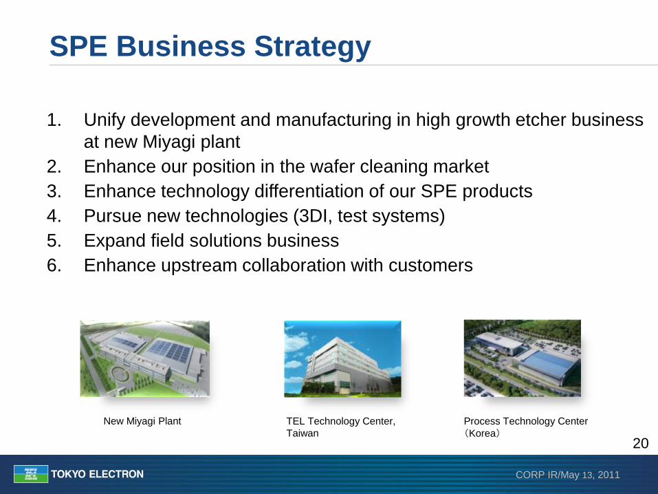
SPE Business Strategy
TEL Technology Center,
Taiwan
Process Technology Center
(Korea)
New Miyagi Plant
1. Unify development and manufacturing in high growth etcher business
at new Miyagi plant
2. Enhance our position in the wafer cleaning market
3. Enhance technology differentiation of our SPE products
4. Pursue new technologies (3DI, test systems)
5. Expand field solutions business
6. Enhance upstream collaboration with customers
CORP IR/May 13, 2011
21
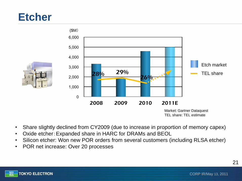
Etch market
TEL share
Market: Gartner Dataquest
TEL share: TEL estimate
Etcher
• Share slightly declined from CY2009 (due to increase in proportion of memory capex)
• Oxide etcher:Expanded share in HARC for DRAMs and BEOL
• Silicon etcher: Won new POR orders from several customers (including RLSA etcher)
• POR net increase: Over 20 processes
0
1,000
2,000
3,000
4,000
5,000
6,000
2008 2009 2010 2011E
28% 29% 26%
($M)
CORP IR/May 13, 2011
22
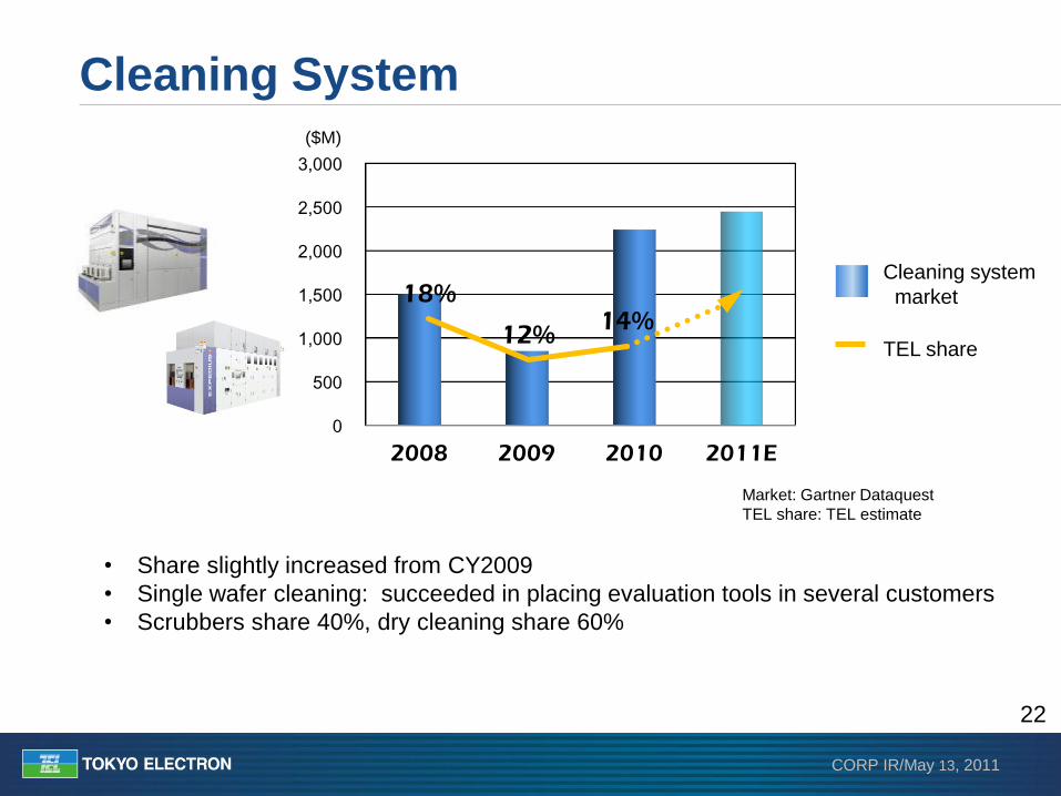
Cleaning System
• Share slightly increased from CY2009
• Single wafer cleaning: succeeded in placing evaluation tools in several customers
• Scrubbers share 40%, dry cleaning share 60%
Market: Gartner Dataquest
TEL share: TEL estimate
Cleaning system
market
TEL share
0
500
1,000
1,500
2,000
2,500
3,000
2008 2009 2010 2011E
18%
12% 14%
($M)
CORP IR/May 13, 2011
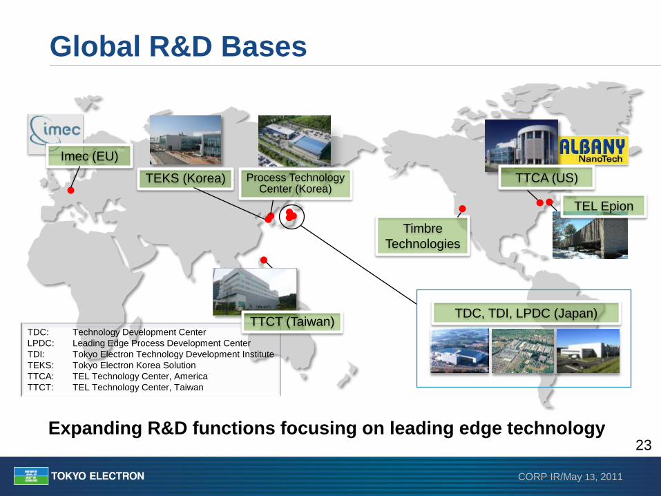
23 Expanding R&D functions focusing on leading edge technology
Global R&D Bases
TDC: Technology Development Center
LPDC: Leading Edge Process Development Center
TDI: Tokyo Electron Technology Development Institute
TEKS: Tokyo Electron Korea Solution
TTCA: TEL Technology Center, America
TTCT: TEL Technology Center, Taiwan
Timbre
Technologies
Imec (EU)
TDC, TDI, LPDC (Japan) TTCT (Taiwan)
TEKS (Korea) TTCA (US) Process Technology Center (Korea)
TEL Epion
CORP IR/May 13, 2011
24
Coater /Developer
• Maintain/grow share for immersion lithography
• Develop technology with EUV lithography products in an inline
environment
Thermal processing system
• Grow share and enhance position especially in Korean market
• Strengthen business base through full-scale entry into ALD and other
new markets
Single wafer deposition system
• Develop new products to address broad needs in metal film deposition
• Establish process using Ru and lead its broad adoption
RLSA
• Accelerate widespread sales for low-damage Poly etch processes
• Build a ¥50 billion business including application of CVD
Main Businesses: Key Actions in FY2012
CORP IR/May 13, 2011
25
3DI
• Promote evaluation and adoption of etching/deposition/bonding
tools by multiple customers
• Expand sales of reverse exposure Fusion Bonder for CIS*
Test system
• Further enhance profitability
• Develop new systems to meet decline in test costs
Field solutions
• Respond flexibly to new investment and expansion mainly in the
commodity device market
• Targeting ¥150 billion sales through used equipment, modification
and service contract business
CIS: C-MOS Image Sensor
Main Businesses: Key Actions in FY2012
CORP IR/May 13, 2011
26
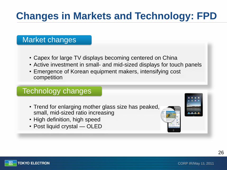
Changes in Markets and Technology: FPD
• Capex for large TV displays becoming centered on China
• Active investment in small- and mid-sized displays for touch panels
• Emergence of Korean equipment makers, intensifying cost competition
Market changes
• Trend for enlarging mother glass size has peaked,
small, mid-sized ratio increasing
• High definition, high speed
• Post liquid crystal — OLED
Technology changes
CORP IR/May 13, 2011
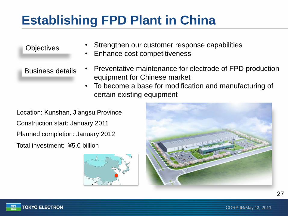
27
Business details
Objectives
Establishing FPD Plant in China
• Preventative maintenance for electrode of FPD production
equipment for Chinese market
• To become a base for modification and manufacturing of
certain existing equipment
• Strengthen our customer response capabilities
• Enhance cost competitiveness
Location: Kunshan, Jiangsu Province Construction start: January 2011
Planned completion: January 2012
Total investment: ¥5.0 billion
CORP IR/May 13, 2011
28
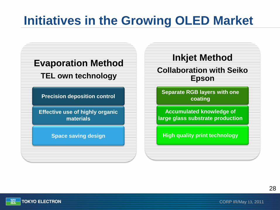
Evaporation Method
TEL own technology
Precision deposition control
Effective use of highly organic
materials
Space saving design
Inkjet Method
Collaboration with Seiko Epson
Separate RGB layers with one
coating
Accumulated knowledge of
large glass substrate production
High quality print technology
Initiatives in the Growing OLED Market
CORP IR/May 13, 2011
29
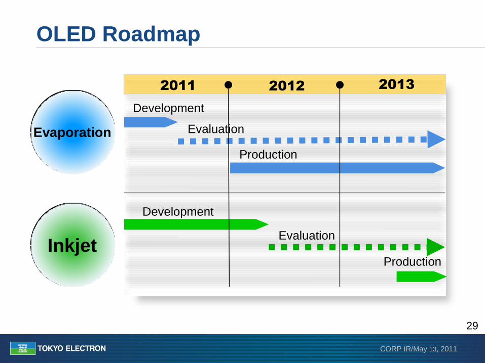
OLED Roadmap
Evaporation
Inkjet
Development
Evaluation
Production
Development
Evaluation
Production
2011 2012 2013
CORP IR/May 13, 2011
30
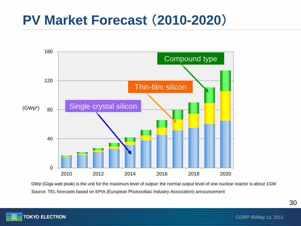
PV Market Forecast (2010-2020)
0
40
80
120
160
2010 2012 2014 2016 2018 2020
Single crystal silicon
Thin-film silicon
Compound type
(GWp*)
Source: TEL forecasts based on EPIA (European Photovoltaic Industry Association) announcement
GWp (Giga watt peak) is the unit for the maximum level of output: the normal output level of one nuclear reactor is about 1GW
CORP IR/May 13, 2011
31
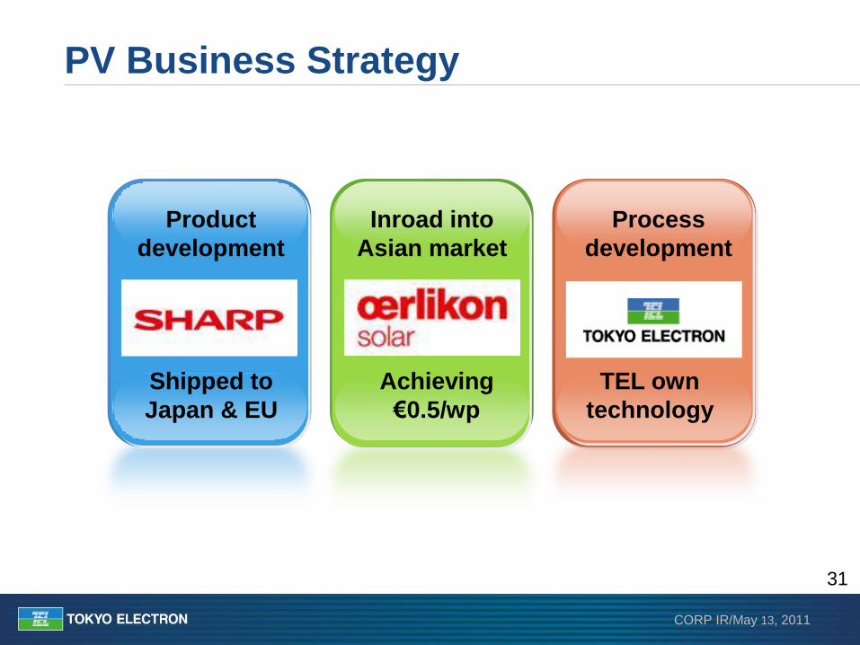
Product
development
Process
development
Inroad into
Asian market
PV Business Strategy
Achieving
€0.5/wp
TEL own
technology
Shipped to
Japan & EU
CORP IR/May 13, 2011
32
Establish TEL Technology Center Tsukuba
Expected benefits
Objectives
• Collaborate with research institutes and universities etc.
in Japan’s largest research location
• Promote networking with other industries
• Recruit top class engineers
• Accelerate R&D in base and core technologies
• Develop technology to raise efficiency of thin film Si PVE
Location: Tsukuba, Ibaraki
Construction start: August 2011
Planned completion: March 2012
Total investment: ¥7.0 billion
Staffing: approx. 100
CORP IR/May 13, 2011
33
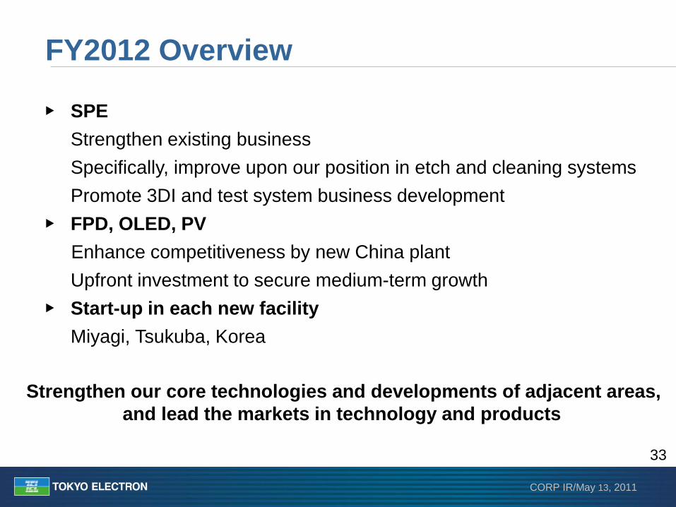
▶ SPE
Strengthen existing business
Specifically, improve upon our position in etch and cleaning systems
Promote 3DI and test system business development
▶ FPD, OLED, PV
Enhance competitiveness by new China plant
Upfront investment to secure medium-term growth
▶ Start-up in each new facility
Miyagi, Tsukuba, Korea
FY2012 Overview
Strengthen our core technologies and developments of adjacent areas,
and lead the markets in technology and products
CORP IR/May 13, 2011
34
Disclaimer regarding forward-looking statement
Forecast of TEL’s performance and future prospects and other sort of information
published are made based on information available at the time of publication. Actual
performance and results may differ significantly from the forecast described here due to
changes in various external and internal factors, including the economic situation,
semiconductor/FPD/PV market conditions, intensification of sales competition, safety and
product quality management, and intellectual property-related risks.
Processing of numbers
For the amount listed, because fractions are rounded down, there may be the cases
where the total for certain account titles does not correspond to the sum of the respective
figures for account titles. Percentages are calculated using full amounts, before rounding.
Exchange Risk
In principle, export sales of Tokyo Electron’s mainstay semiconductor and FPD/PV cell
production equipment are denominated in yen. While some settlements are denominated
in dollars, exchange risk is hedged as forward exchange contracts are made individually
at the time of booking. Accordingly, the effect of exchange rates on profits is negligible.
FPD/PV: Flat panel display/Photovoltaic